US7115524B2 - Methods of processing a semiconductor substrate - Google Patents
Methods of processing a semiconductor substrate Download PDFInfo
- Publication number
- US7115524B2 US7115524B2 US10/848,030 US84803004A US7115524B2 US 7115524 B2 US7115524 B2 US 7115524B2 US 84803004 A US84803004 A US 84803004A US 7115524 B2 US7115524 B2 US 7115524B2
- Authority
- US
- United States
- Prior art keywords
- layer
- masking layer
- peripheral region
- semiconductor substrate
- amorphous carbon
- Prior art date
- Legal status (The legal status is an assumption and is not a legal conclusion. Google has not performed a legal analysis and makes no representation as to the accuracy of the status listed.)
- Expired - Fee Related, expires
Links
Images


Classifications
-
- H—ELECTRICITY
- H01—ELECTRIC ELEMENTS
- H01L—SEMICONDUCTOR DEVICES NOT COVERED BY CLASS H10
- H01L21/00—Processes or apparatus adapted for the manufacture or treatment of semiconductor or solid state devices or of parts thereof
- H01L21/02—Manufacture or treatment of semiconductor devices or of parts thereof
- H01L21/04—Manufacture or treatment of semiconductor devices or of parts thereof the devices having at least one potential-jump barrier or surface barrier, e.g. PN junction, depletion layer or carrier concentration layer
- H01L21/18—Manufacture or treatment of semiconductor devices or of parts thereof the devices having at least one potential-jump barrier or surface barrier, e.g. PN junction, depletion layer or carrier concentration layer the devices having semiconductor bodies comprising elements of Group IV of the Periodic System or AIIIBV compounds with or without impurities, e.g. doping materials
- H01L21/30—Treatment of semiconductor bodies using processes or apparatus not provided for in groups H01L21/20 - H01L21/26
- H01L21/31—Treatment of semiconductor bodies using processes or apparatus not provided for in groups H01L21/20 - H01L21/26 to form insulating layers thereon, e.g. for masking or by using photolithographic techniques; After treatment of these layers; Selection of materials for these layers
- H01L21/3105—After-treatment
- H01L21/311—Etching the insulating layers by chemical or physical means
- H01L21/31144—Etching the insulating layers by chemical or physical means using masks
-
- H—ELECTRICITY
- H01—ELECTRIC ELEMENTS
- H01L—SEMICONDUCTOR DEVICES NOT COVERED BY CLASS H10
- H01L21/00—Processes or apparatus adapted for the manufacture or treatment of semiconductor or solid state devices or of parts thereof
- H01L21/02—Manufacture or treatment of semiconductor devices or of parts thereof
- H01L21/027—Making masks on semiconductor bodies for further photolithographic processing not provided for in group H01L21/18 or H01L21/34
- H01L21/033—Making masks on semiconductor bodies for further photolithographic processing not provided for in group H01L21/18 or H01L21/34 comprising inorganic layers
- H01L21/0332—Making masks on semiconductor bodies for further photolithographic processing not provided for in group H01L21/18 or H01L21/34 comprising inorganic layers characterised by their composition, e.g. multilayer masks, materials
-
- H—ELECTRICITY
- H01—ELECTRIC ELEMENTS
- H01L—SEMICONDUCTOR DEVICES NOT COVERED BY CLASS H10
- H01L21/00—Processes or apparatus adapted for the manufacture or treatment of semiconductor or solid state devices or of parts thereof
- H01L21/02—Manufacture or treatment of semiconductor devices or of parts thereof
- H01L21/027—Making masks on semiconductor bodies for further photolithographic processing not provided for in group H01L21/18 or H01L21/34
- H01L21/033—Making masks on semiconductor bodies for further photolithographic processing not provided for in group H01L21/18 or H01L21/34 comprising inorganic layers
- H01L21/0334—Making masks on semiconductor bodies for further photolithographic processing not provided for in group H01L21/18 or H01L21/34 comprising inorganic layers characterised by their size, orientation, disposition, behaviour, shape, in horizontal or vertical plane
Definitions
- This invention relates to methods of processing a semiconductor substrate.
- Integrated circuits are typically formed on a semiconductor substrate, such as a silicon wafer or other semiconducting material.
- a semiconductor substrate such as a silicon wafer or other semiconducting material.
- layers of various materials which are either semiconducting, conducting or insulating are utilized to form the integrated circuits.
- the various materials are doped, ion implanted, deposited, etched, grown, etc. using various processes. Further, a continuing goal in semiconductor processing is to continue to strive to reduce the size of individual electronic components, thereby enabling smaller and denser integrated circuitry.
- photolithography typically includes deposition of a photoresist layer which can be processed to modify the solubility of such layer in certain solvents. For example, portions of the photoresist layer can be exposed through a mask/reticle to change the solvent solubility of the exposed regions versus the unexposed regions compared to the as-deposited state. Thereafter, the exposed or unexposed portions can be removed, depending on the type of photoresist, thereby leaving a masking pattern of the photoresist on the substrate. Adjacent areas of the substrate next to the masked portions can be processed, for example by etching or ion implanting, to effect the desired processing of the substrate adjacent the masking material.
- multiple different layers of photoresist are utilized in a given masking/photolithographic step.
- the photolithographic masking and patterning might be combined with one or more other layers.
- One such process forms what is commonly referred to as a “hard mask” over the substrate prior to deposition of the photoresist layer or layers.
- the photoresist layer is then patterned, for example as described above, to form masking blocks over the hard mask.
- the hard mask is then etched using the photoresist as a mask to transfer the pattern of the photoresist of the hard mask.
- the photoresist may or may not be removed immediately thereafter.
- Hard masks such as just described provide a more robust masking pattern than photoresist alone, for example should the photoresist be completely eroded/etched away.
- One material utilized as a hard mask is amorphous carbon.
- the amorphous carbon might be doped with other materials, for example boron.
- the etching typically removes the oxide at a rate of about ten times faster than it removes amorphous carbon.
- an antireflective coating (with or without a hard mask) over which the photoresist is deposited.
- an antireflective coating might be employed intermediate the amorphous carbon and the photoresist layer.
- the antireflective coating might be composed of a single layer, or multiple layers.
- one antireflective coating might be inorganic, and another antireflective coating might be organic.
- an antireflective coating over amorphous carbon comprises a first inorganic layer and a second organic layer.
- Photoresist is deposited thereafter and, after photolighographic exposure and developing, openings are formed through the photoresist to the antireflective layer(s).
- the mask pattern in the photoresist layer is then typically transferred through the antireflective layer(s), and through the amorphous carbon layer, utilizing one or more dry anisotropic etching techniques.
- one or more suitable different chemistries are typically utilized to extend the openings through the layer or layers inwardly of the amorphous carbon layer.
- edge bead which constitutes an excessive, thickened section of resist at the peripheral outer edge of the wafer or substrate.
- the edge bead can be several times as thick as the layer of resist which is more centrally received over the substrate. This can, in some instances, leave an edge bead of resist over the antireflective coating and over amorphous carbon in a peripheral region about the edge of the substrate after the mask pattern has been formed in the amorphous carbon layer.
- Such photoresist in the peripheral region and/or any antireflective coating can cause residual amorphous carbon and antireflective coating to remain on the substrate/wafer edge after dry etching and cleaning. Such can subsequently peel away later, and undesirably cause particle contamination.
- the invention includes methods of processing semiconductor substrates.
- a semiconductor substrate is provided which has an outer surface. Such surface has a peripheral region received about a peripheral edge of the semiconductor substrate.
- a layer comprising amorphous carbon is provided over the substrate outer surface.
- a masking layer is provided outwardly of the amorphous carbon-comprising layer.
- a resist layer is provided outwardly of the masking layer. At least a portion of the peripheral region of the outer surface includes the amorphous carbon-comprising layer and the resist layer, but is substantially void of the masking layer.
- the amorphous carbon-comprising layer is patterned using the resist layer and the masking layer effective to form a mask over the semiconductor substrate. After the patterning, the semiconductor substrate is processed inwardly of the mask through openings formed in the mask.
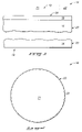
- FIG. 1 is a diagrammatic sectional view of a semiconductor substrate fragment at a point of processing in accordance with an aspect of the invention.
- FIG. 2 is a reduced scale, top plan, view of a substrate incorporating the semiconductor substrate fragment of FIG. 1 .
- FIG. 3 is a view of the FIG. 1 substrate fragment at a processing point subsequent to that depicted by FIG. 1 .
- FIG. 4 is a view of the FIG. 3 substrate fragment at a processing point subsequent to that depicted by FIG. 3 .
- FIG. 5 is a view of the FIG. 1 substrate fragment at a processing point subsequent to that depicted by FIG. 1 , and alternate to that depicted by FIG. 3 .
- FIG. 6 is a view of the FIG. 4 substrate fragment at a processing point subsequent to that depicted by FIG. 4 .
- FIG. 7 is a diagrammatic sectional view of a semiconductor substrate fragment at a point of processing in accordance with an aspect of the invention.
- FIG. 8 is a view of the FIG. 7 substrate fragment at a processing point subsequent to that depicted by FIG. 7 .
- FIG. 9 is a view of the FIG. 8 substrate fragment at a processing point subsequent to that depicted by FIG. 8 .
- FIG. 10 is a view of the FIG. 9 substrate fragment at a processing point subsequent to that depicted by FIG. 9 .
- FIG. 11 is a diagrammatic sectional view of a semiconductor substrate fragment at a point of processing in accordance with an aspect of the invention.
- FIG. 12 is a view of the FIG. 11 substrate fragment at a processing point subsequent to that depicted by FIG. 11 .
- FIG. 13 is a view of the FIG. 12 substrate fragment at a processing point subsequent to that depicted by FIG. 12 .
- a semiconductor substrate is indicated generally with reference numeral 10 , and comprises a first or front side 12 and a second or back side 14 .
- semiconductor substrate or “semiconductive substrate” is defined to mean any construction comprising semiconductive material, including, but not limited to, bulk semiconductive materials such as a semiconductive wafer (either alone or in assemblies comprising other materials thereon), and semiconductive material layers (either alone or in assemblies comprising other materials).
- substrate refers to any supporting structure, including, but not limited to, the semiconductive substrates described above.
- substrate 10 is depicted as comprising bulk semiconductor material 16 , such as monocrystalline silicon.
- a layer 18 is formed over substrate material 16 on substrate first side 12 .
- layer 18 will be etched, although any other processing thereof (whether existing or yet-to-be developed) using a masking as described below is also, of course, contemplated.
- One exemplary material for layer 18 includes a silicon dioxide, such as borophosphosilicate glass (BPSG).
- BPSG borophosphosilicate glass
- Semiconductor substrate 10 can be considered as having an outer surface 20 on first side 12 . Substrate 10 is encompassed by a peripheral edge 23 . Outer surface 20 can be considered as having a peripheral region 22 received about edge 23 . Outer surface 20 can also be considered as having a central region 21 received radially inward of peripheral region 22 . In the context of the processing which follows, peripheral region 22 is preferably at least 0.5 mm wide, and more preferably from 0.5 mm to 3.5 mm wide.
- a layer 26 comprising amorphous carbon has been provided over (and preferably “on”, as shown) substrate outer surface 20 .
- a masking layer 31 is provided to be received outwardly of amorphous carbon-comprising layer 26
- a resist layer 30 (preferably a photoresist) is provided to be received outwardly of masking layer 31 .
- At least a portion of the peripheral region 22 outer surface 20 comprises amorphous carbon-comprising layer 26 and resist layer 30 , but is substantially void of masking layer 31 .
- all of peripheral region 22 is void of masking layer 31 .
- the portion of peripheral region 22 not having masking layer 31 is some portion less than all of the peripheral region, with in one embodiment such portion being at least a majority portion of the peripheral region.
- Amorphous carbon-comprising layer 26 might comprise, consist essentially of, or consist of amorphous carbon, and which is either doped or undoped, for example with boron.
- a preferred thickness range is from 500 Angstroms to 10,000 Angstroms.
- layer 26 might be provided by chemical vapor deposition using at least one of C 2 H 6 , C 2 H 4 , C 2 H 2 , C 3 H 6 and C 3 H 8 . Further where boron doping is desired, the chemical vapor depositing might use at least one of B 2 H 6 , B 4 H 10 and BH 3 CO, thereby forming the amorphous carbon to be in situ boron doped as-deposited.
- masking layer 31 comprises an antireflective coating, and more preferably an inorganic antireflective coating, for example silicon oxynitrides (SiO x N y ).
- a preferred thickness range is from 100 Angstroms to 1,000 Angstroms.
- other exemplary materials independent of antireflective characteristics for masking layer 31 include carbides (i.e., BC, SiC), silicon in elemental crystalline form (i.e., monocrystalline silicon or polycrystalline silicon), conductive elemental metals (i.e., W, Ti).
- alloys of elemental metals conductive metal compounds (i.e., conductive metal nitrides, for example TiN and WN), other non-conductive nitrides (i.e., BN, Si 3 N 4 ) and silicon oxides (i.e., SiO 2 ).
- conductive metal compounds i.e., conductive metal nitrides, for example TiN and WN
- other non-conductive nitrides i.e., BN, Si 3 N 4
- silicon oxides i.e., SiO 2
- a material different from that of the masking layer is provided intermediate the resist and the amorphous carbon-comprising layer.
- example materials include antireflective coatings, more preferably organic antireflective coatings, such as BARCs, for example DUV112 available from Brewer Science of Rolla, Mo.
- FIG. 3 depicts such a material 32 , and which is received over masking layer 31 and over peripheral region 22 .
- a preferred thickness range is from 100 Angstroms to 1,000 Angstroms.
- Resist layer 30 is preferably a photoresist, and can be either a negative photoresist or a positive photoresist. Positive photoresists are preferred.
- resist layer 30 is shown to be thicker over at least some portion of peripheral region 22 than over central region 21 , at least at this point in the process, although such is in no way required in all aspects of the invention.
- resist layer 30 is shown as having been patterned in some manner to form a pair of openings 34 therein.
- An exemplary technique includes photolithographic exposure to suitable incident radiation and subsequent development.
- amorphous carbon-comprising layer 26 has been patterned, at least in part, using resist layer 30 of FIG. 3 (not shown in FIG. 4 ) and masking layer 31 of FIG. 3 (not shown in FIG. 4 ) effective to form a mask 38 over/as part of semiconductor substrate 10 .
- FIG. 4 also depicts resist layer 30 and masking layer 31 as having been removed at the conclusion of formation of mask 38 .
- preferred techniques for processing the substrate of FIG. 3 to produce the substrate of FIG. 4 include a suitable dry anisotropic etch using a CF 4 chemistry to extend openings 34 in FIG.
- amorphous carbon-comprising layer 26 where, for example, layers 31 and 32 comprise SiO x N y and Brewer Science BARC products respectively Only some, a majority, most or all of photoresist 30 might be removed during such etching depending upon the composition of resist 30 , its thickness, and the etching chemistry utilized. Regardless, after etching through layers 31 and 32 , openings 34 can be extended into amorphous carbon-comprising layer 26 utilizing a dry anisotropic etch preferably principally including a SO 2 chemistry.
- FIG. 3 essentially depicts material 32 being received over the portion of peripheral region 22 during the patterning to produce FIG. 4 .
- material 32 might not be received over the portion of peripheral region 22 during the patterning to produce FIG. 4 , for example as shown in FIG. 5 for a substrate 100 as an exemplary alternate to FIG. 3 .
- material 32 might be eliminated/not used altogether, or alternately even multiple materials used in addition to masking layer 31 .
- the thickened resist portion shown over at least some of peripheral region 22 may or may not occur at all, and at different times if such does occur. For example, it may appear only after a partial or initial dry develop of layer 31 (and material 32 when used), or only after such layer(s) has/have been fully developed by extending openings 34 therethrough, or maybe not until etching completely through layer 26 .
- a reason is that during a dry etch, polymer formation from such etch can occur faster at the periphery of the substrate than centrally. This polymer can form on top of the deposited resist and block removal of material therebeneath during the dry etch. Material beneath the resist in turn can block amorphous carbon removal during strip of the resist.
- the masking layer 31 (most commonly an inorganic antireflective coating) from at least some, and preferably all, of the peripheral region can overcome this problem.
- the peripheral region might be thicker due to reasons other than photoresist application and processing, for example due to a thicker portion of the amorphous carbon being formed at the periphery during its formation.
- mask 38 masks at least a portion of peripheral region 22 , and more preferably masks all of peripheral region 22 , and with at least amorphous carbon-comprising layer 26 .
- Some of amorphous carbon-comprising layer 26 might also be etched in peripheral region 22 as compared to central region 21 , as shown, due to lack of masking layer 31 in peripheral region 22 .
- semiconductor substrate 10 has been processed inwardly of mask 38 through openings 34 formed in mask 38 .
- the typical and preferred form of processing is etching, although other forms of processing, whether existing or yet-to-be developed, might additionally or alternately be utilized (i.e., ion implanting).
- mask 38 /layer 26 would then be removed, although such is of course not required.
- the provision of masking layer 31 might result, in part, from forming some or all of masking layer 31 over peripheral region 22 and subsequently removing it from over all or a portion of peripheral region 22 .
- the provision of masking layer 31 might occur by deposition methods wherein the depositing of a masking layer 31 does not ever occur in some or all of a portion of peripheral region 22 .
- an amorphous carbon-comprising layer 26 could be blanketly deposited over an entirety of semiconductor substrate outer surface 20 . Thereafter, all of the peripheral region might be masked while depositing a masking layer 31 over central region 21 such that peripheral region 22 is substantially void of masking layer 31 .
- a substantially anisotropic deposition for example using dry plasma directional deposition wherein a masking shield/rim is positioned over the substrate to mask all of peripheral region 22 while leaving central portion 21 exposed to the deposition of masking layer 31 .
- a resist could be blanketly deposited over an entirety of the semiconductor substrate outer surface. Patterning of the amorphous carbon-comprising layer and subsequent processing of the semiconductor substrate inwardly of the mask could then occur, for example as described above.
- the invention also, by way of example only, contemplates forming the masking layer over the peripheral region, and subsequently removing it from over at least a portion of the peripheral region.
- a first exemplary such process is described with reference to FIGS. 7–10
- a second exemplary process is described with reference to FIGS. 11–13 .
- an alternate embodiment semiconductor substrate is indicated generally with reference numeral 10 a .
- Amorphous carbon-comprising layer 26 has been blanketly deposited over an entirety of semiconductor substrate outer surface 20 .
- a masking layer 31 a and an optional another material 32 a have been blanketly deposited over amorphous carbon-comprising layer 26 over an entirety of semiconductor substrate outer surface 20 .
- a first resist layer 30 has been blanketly deposited over masking layer 31 a (and over material 32 a ) over an entirety of semiconductor substrate outer surface 20 . Exemplary thicknesses and materials are as described above with the first embodiments.
- first layer of resist 30 has been removed from over all of peripheral region 22 while leaving central region 21 covered with first layer of resist 30 .
- Any existing or yet-to-be developed method(s) for forming the exemplary substrate FIG. 8 processing is of course contemplated.
- One exemplary (but lesser preferred) method includes a photolithographic masking step and subsequent wet develop.
- a more preferred technique comprises spraying a resist solvent onto the substrate while spinning the substrate, for example by some form of chemical edge bead removal of photoresist as is conventional in the existing state of the art.
- One such process would spray a suitable photoresist solvent onto back side 14 of substrate 10 a while spinning the substrate.
- a method might be utilized whereby a suitable photoresist solvent is sprayed peripherally onto front side 12 of a spinning substrate and, regardless, ideally in such a manner that photoresist 30 remains over central region 21 and is completely removed from peripheral region 22 .
- a suitable photoresist solvent is sprayed peripherally onto front side 12 of a spinning substrate and, regardless, ideally in such a manner that photoresist 30 remains over central region 21 and is completely removed from peripheral region 22 .
- an exemplary solution for doing so includes RER450 available from Arch Chemicals of Norwalk, Conn., and understood to principally comprise diacetone alcohol.
- peripheral region masking layer 31 a (and preferably all, as shown) is removed from over peripheral region 22 , while central region 21 remains covered with some portion of first layer of resist 30 .
- An exemplary technique for doing so includes dry anisotropic etching utilizing resist layer 30 as a mask, for example using CF 4 and/or other fluorocarbon chemistries. Where material 32 a is used, a corresponding at least some of the peripheral material 32 a is also of course removed from over peripheral region 22 .
- first layer of resist 30 After removing at least some of masking layer 31 a from peripheral region 22 , the remaining portions of first layer of resist 30 are removed from the substrate.
- any suitable existing or yet-to-be developed methods can be utilized, for example using an O 2 plasma ashing processing.
- a second layer of resist 50 is blanketly deposited over an entirety of semiconductor substrate outer surface 20 to produce, in the exemplary described process, essentially the same substrate depicted by FIG. 5 .
- Subsequent patterning of the amorphous carbon-comprising layer and processing of the substrate inwardly thereof can then be conducted as described above, or otherwise.
- FIGS. 11–13 a method is described with reference to FIGS. 11–13 with respect to a semiconductor substrate 10 b.
- Like numerals from the first described embodiments are utilized where appropriate, with differences being indicated by the suffix “b” or with different numerals.
- an amorphous carbon-comprising layer 26 has been blanketly deposited over an entirety of semiconductor substrate outer surface 20 .
- a masking layer 31 b has been blanketly deposited over amorphous carbon-comprising layer 26 over an entirety of semiconductor substrate outer surface 20 .
- An optional material 32 b has also been deposited, over layer 31 b as shown. Exemplary thicknesses and materials are as described above with the first embodiments.
- masking layer 31 b (and preferably all, as shown) has been removed from over all of peripheral region 22 while leaving central region 21 covered with masking layer 31 b.
- One exemplary manner of doing so is as described above with respect to FIGS. 7–10 .
- material 32 b is used, a corresponding at least some of the peripheral material 32 b is also of course removed from over peripheral region 22 .
- the removing of at least some of the masking layer from over all of the peripheral region could comprise spraying a masking layer solvent onto the substrate while spinning the substrate.
- the masking layer could be removed in a manner analogous to that described above with respect to the FIGS. 7–10 embodiment whereby resist 30 was removed from over the peripheral region.
- one or more suitable masking layer solvents (including a material 32 b solvent where material 32 b is used) could be sprayed onto back side 14 of substrate 10 b while spinning the substrate, and/or peripherally onto the front side of the substrate.
- multiple different solvents might be sprayed onto the wafer.
- HF solutions will remove SiO x N y layers
- the above exemplary RER450 solution will remove organic antireflective coatings.
- a resist layer 30 has been blanketly deposited over an entirety of semiconductor substrate outer surface 20 , and otherwise processed to produce the exemplary construction of FIG. 5 . Subsequent patterning of the amorphous carbon-comprising layer and processing the semiconductor substrate inwardly of the resulting mask can, of course, occur as described in the above exemplary first embodiment.
- the resist in only the peripheral region is exposed to incident radiation at an energy density of at least 200 mW/cm 2 (more preferably an energy density of at least 300 mW/cm 2 ) for a period of time effective to prevent resist dissolution in the peripheral region during a development process of the resist.
- An exemplary preferred technique would use a broadband UV lamp at 300 mW/cm 2 for 60 seconds.
Landscapes
- Engineering & Computer Science (AREA)
- Physics & Mathematics (AREA)
- Condensed Matter Physics & Semiconductors (AREA)
- General Physics & Mathematics (AREA)
- Manufacturing & Machinery (AREA)
- Computer Hardware Design (AREA)
- Microelectronics & Electronic Packaging (AREA)
- Power Engineering (AREA)
- Chemical & Material Sciences (AREA)
- Inorganic Chemistry (AREA)
- Drying Of Semiconductors (AREA)
- Exposure Of Semiconductors, Excluding Electron Or Ion Beam Exposure (AREA)
Abstract
Description
Claims (112)
Priority Applications (2)
| Application Number | Priority Date | Filing Date | Title |
|---|---|---|---|
| US10/848,030 US7115524B2 (en) | 2004-05-17 | 2004-05-17 | Methods of processing a semiconductor substrate |
| US11/490,807 US7432212B2 (en) | 2004-05-17 | 2006-07-20 | Methods of processing a semiconductor substrate |
Applications Claiming Priority (1)
| Application Number | Priority Date | Filing Date | Title |
|---|---|---|---|
| US10/848,030 US7115524B2 (en) | 2004-05-17 | 2004-05-17 | Methods of processing a semiconductor substrate |
Related Child Applications (1)
| Application Number | Title | Priority Date | Filing Date |
|---|---|---|---|
| US11/490,807 Continuation US7432212B2 (en) | 2004-05-17 | 2006-07-20 | Methods of processing a semiconductor substrate |
Publications (2)
| Publication Number | Publication Date |
|---|---|
| US20050255702A1 US20050255702A1 (en) | 2005-11-17 |
| US7115524B2 true US7115524B2 (en) | 2006-10-03 |
Family
ID=35309984
Family Applications (2)
| Application Number | Title | Priority Date | Filing Date |
|---|---|---|---|
| US10/848,030 Expired - Fee Related US7115524B2 (en) | 2004-05-17 | 2004-05-17 | Methods of processing a semiconductor substrate |
| US11/490,807 Expired - Fee Related US7432212B2 (en) | 2004-05-17 | 2006-07-20 | Methods of processing a semiconductor substrate |
Family Applications After (1)
| Application Number | Title | Priority Date | Filing Date |
|---|---|---|---|
| US11/490,807 Expired - Fee Related US7432212B2 (en) | 2004-05-17 | 2006-07-20 | Methods of processing a semiconductor substrate |
Country Status (1)
| Country | Link |
|---|---|
| US (2) | US7115524B2 (en) |
Cited By (3)
| Publication number | Priority date | Publication date | Assignee | Title |
|---|---|---|---|---|
| US20060115772A1 (en) * | 2004-11-26 | 2006-06-01 | Samsung Electronics Co., Ltd. | Polymeric tetrahedral carbon films, methods of forming the same and methods of forming fine patterns using the same |
| US20070082483A1 (en) * | 2005-10-12 | 2007-04-12 | Samsung Electronics Co., Ltd. | Method of etching carbon-containing layer and method of fabricating semiconductor device |
| US7772094B2 (en) | 2007-12-28 | 2010-08-10 | Texas Instuments Incorporated | Implant damage of layer for easy removal and reduced silicon recess |
Families Citing this family (11)
| Publication number | Priority date | Publication date | Assignee | Title |
|---|---|---|---|---|
| US7105431B2 (en) * | 2003-08-22 | 2006-09-12 | Micron Technology, Inc. | Masking methods |
| US7354631B2 (en) * | 2003-11-06 | 2008-04-08 | Micron Technology, Inc. | Chemical vapor deposition apparatus and methods |
| US7115524B2 (en) * | 2004-05-17 | 2006-10-03 | Micron Technology, Inc. | Methods of processing a semiconductor substrate |
| US7572482B2 (en) * | 2006-04-14 | 2009-08-11 | Bae Systems Information And Electronic Systems Integration Inc. | Photo-patterned carbon electronics |
| KR100755076B1 (en) | 2006-06-29 | 2007-09-06 | 주식회사 하이닉스반도체 | Method for forming metal film pattern in semiconductor device |
| US7553770B2 (en) * | 2007-06-06 | 2009-06-30 | Micron Technology, Inc. | Reverse masking profile improvements in high aspect ratio etch |
| US7824846B2 (en) * | 2007-09-19 | 2010-11-02 | International Business Machines Corporation | Tapered edge bead removal process for immersion lithography |
| US20130084685A1 (en) * | 2011-09-30 | 2013-04-04 | Taiwan Semiconductor Manufacturing Company, Ltd. | Methods for Ion Implantation |
| US11120479B2 (en) | 2016-01-25 | 2021-09-14 | Magnite, Inc. | Platform for programmatic advertising |
| US11288699B2 (en) | 2018-07-13 | 2022-03-29 | Pubwise, LLLP | Digital advertising platform with demand path optimization |
| US11270890B2 (en) * | 2018-12-14 | 2022-03-08 | Lam Research Corporation | Etching carbon layer using doped carbon as a hard mask |
Citations (46)
| Publication number | Priority date | Publication date | Assignee | Title |
|---|---|---|---|---|
| US4382100A (en) | 1976-08-13 | 1983-05-03 | National Research Development Corporation | Application of a layer of carbonaceous material to a surface |
| US4436797A (en) | 1982-06-30 | 1984-03-13 | International Business Machines Corporation | X-Ray mask |
| US4510176A (en) | 1983-09-26 | 1985-04-09 | At&T Bell Laboratories | Removal of coating from periphery of a semiconductor wafer |
| US4675265A (en) | 1985-03-26 | 1987-06-23 | Fuji Electric Co., Ltd. | Electrophotographic light-sensitive element with amorphous C overlayer |
| US4732785A (en) | 1986-09-26 | 1988-03-22 | Motorola, Inc. | Edge bead removal process for spin on films |
| US4886728A (en) | 1988-01-06 | 1989-12-12 | Olin Hunt Specialty Products Inc. | Use of particular mixtures of ethyl lactate and methyl ethyl ketone to remove undesirable peripheral material (e.g. edge beads) from photoresist-coated substrates |
| US4994404A (en) | 1989-08-28 | 1991-02-19 | Motorola, Inc. | Method for forming a lightly-doped drain (LDD) structure in a semiconductor device |
| US5433794A (en) | 1992-12-10 | 1995-07-18 | Micron Technology, Inc. | Spacers used to form isolation trenches with improved corners |
| US5656128A (en) | 1993-03-26 | 1997-08-12 | Fujitsu Limited | Reduction of reflection by amorphous carbon |
| US5679215A (en) | 1996-01-02 | 1997-10-21 | Lam Research Corporation | Method of in situ cleaning a vacuum plasma processing chamber |
| US5754390A (en) | 1996-01-23 | 1998-05-19 | Micron Technology, Inc. | Integrated capacitor bottom electrode for use with conformal dielectric |
| US5788778A (en) | 1996-09-16 | 1998-08-04 | Applied Komatsu Technology, Inc. | Deposition chamber cleaning technique using a high power remote excitation source |
| US5814433A (en) | 1996-05-17 | 1998-09-29 | Clariant Finance (Bvi) Limited | Use of mixtures of ethyl lactate and N-methyl pyrollidone as an edge bead remover for photoresists |
| JPH11214290A (en) | 1998-01-29 | 1999-08-06 | Miyazaki Oki Electric Co Ltd | Manufacture of resist film and semiconductor device |
| US5952050A (en) | 1996-02-27 | 1999-09-14 | Micron Technology, Inc. | Chemical dispensing system for semiconductor wafer processing |
| US6188097B1 (en) | 1997-07-02 | 2001-02-13 | Micron Technology, Inc. | Rough electrode (high surface area) from Ti and TiN |
| US6218237B1 (en) | 1996-01-03 | 2001-04-17 | Micron Technology, Inc. | Method of forming a capacitor |
| US20010023123A1 (en) | 1999-12-24 | 2001-09-20 | Kim Jin-Woong | Method for forming semiconductor device having low parasite capacitance using air gap and self-aligned contact plug |
| US6297112B1 (en) | 2000-02-04 | 2001-10-02 | United Microelectronics Corp. | Method of forming a MOS transistor |
| US6306702B1 (en) | 1999-08-24 | 2001-10-23 | Advanced Micro Devices, Inc. | Dual spacer method of forming CMOS transistors with substantially the same sub 0.25 micron gate length |
| US6333255B1 (en) | 1997-08-21 | 2001-12-25 | Matsushita Electronics Corporation | Method for making semiconductor device containing low carbon film for interconnect structures |
| US6342423B1 (en) | 1999-09-24 | 2002-01-29 | Advanced Micro Devices, Inc. | MOS-type transistor processing utilizing UV-nitride removable spacer and HF etch |
| US6344396B1 (en) | 1999-09-24 | 2002-02-05 | Advanced Micro Devices, Inc. | Removable spacer technology using ion implantation for forming asymmetric MOS transistors |
| US6369431B1 (en) | 1996-02-23 | 2002-04-09 | Micron Technology, Inc. | Method for forming conductors in semiconductor devices |
| US6368986B1 (en) | 2000-08-31 | 2002-04-09 | Micron Technology, Inc. | Use of selective ozone TEOS oxide to create variable thickness layers and spacers |
| US20020088707A1 (en) | 1998-07-01 | 2002-07-11 | Towle Steven N. | Method for improving thermal stability of fluorinated amorphous carbon low dielectric constant materials |
| US20020132451A1 (en) * | 1998-02-04 | 2002-09-19 | Yutaka Akino | Semiconductor substrate and method of manufacturing the same |
| US6453916B1 (en) | 2000-06-09 | 2002-09-24 | Advanced Micro Devices, Inc. | Low angle solvent dispense nozzle design for front-side edge bead removal in photolithography resist process |
| US6472283B1 (en) | 1999-09-24 | 2002-10-29 | Advanced Micro Devices, Inc. | MOS transistor processing utilizing UV-nitride removable spacer and HF etch |
| US6475868B1 (en) | 1999-08-18 | 2002-11-05 | Advanced Micro Devices, Inc. | Oxygen implantation for reduction of junction capacitance in MOS transistors |
| US20020185687A1 (en) | 2001-06-06 | 2002-12-12 | Nec Corporation | Semiconductor device and method of fabricating the same |
| US6495312B1 (en) | 2001-02-01 | 2002-12-17 | Lsi Logic Corporation | Method and apparatus for removing photoresist edge beads from thin film substrates |
| US6500756B1 (en) | 2002-06-28 | 2002-12-31 | Advanced Micro Devices, Inc. | Method of forming sub-lithographic spaces between polysilicon lines |
| US20030001187A1 (en) | 2000-03-23 | 2003-01-02 | Micron Technologh, Inc. | Structures and methods for enhancing capacitors in integrated circuits |
| US6524775B1 (en) | 2000-10-20 | 2003-02-25 | Clariant Finance (Bvi) Limited | Edge bead remover for thick film photoresists |
| US20030045121A1 (en) * | 2001-09-03 | 2003-03-06 | Kabushiki Kaisha Toshiba | Fabrication method and wafer structure of semiconductor device using low-k film |
| US20030073309A1 (en) | 2001-10-16 | 2003-04-17 | Applied Materials, Inc. | Apparatus and method for edge bead removal |
| US6559017B1 (en) | 2002-06-13 | 2003-05-06 | Advanced Micro Devices, Inc. | Method of using amorphous carbon as spacer material in a disposable spacer process |
| US6605514B1 (en) | 2002-07-31 | 2003-08-12 | Advanced Micro Devices, Inc. | Planar finFET patterning using amorphous carbon |
| US6653220B2 (en) | 1996-10-31 | 2003-11-25 | Micron Technology, Inc. | Advance metallization process |
| US20040043574A1 (en) | 2002-09-03 | 2004-03-04 | Steiner Kurt George | Protruding spacers for self-aligned contacts |
| US20040043262A1 (en) | 2001-12-25 | 2004-03-04 | Tomonori Asou | Hydrogen generation system and fuel cell system having the same |
| US6750127B1 (en) | 2003-02-14 | 2004-06-15 | Advanced Micro Devices, Inc. | Method for fabricating a semiconductor device using amorphous carbon having improved etch resistance |
| US20050042879A1 (en) | 2003-08-22 | 2005-02-24 | Zhiping Yin | Masking methods |
| US6875664B1 (en) | 2002-08-29 | 2005-04-05 | Advanced Micro Devices, Inc. | Formation of amorphous carbon ARC stack having graded transition between amorphous carbon and ARC material |
| US20050098105A1 (en) | 2003-11-06 | 2005-05-12 | Fuss Jeff N. | Chemical vapor deposition apparatus and methods |
Family Cites Families (11)
| Publication number | Priority date | Publication date | Assignee | Title |
|---|---|---|---|---|
| DE4206044A1 (en) * | 1992-02-27 | 1993-09-02 | Bayer Ag | COATING AGENT, METHOD FOR THE PRODUCTION THEREOF AND THEIR USE |
| US6291315B1 (en) * | 1996-07-11 | 2001-09-18 | Denso Corporation | Method for etching trench in manufacturing semiconductor devices |
| FR2758884B1 (en) * | 1997-01-30 | 1999-04-02 | Bio Merieux | METHOD FOR ISOLATING, IN PARTICULAR DETECTING OR QUANTIFYING AN ANALYTE IN A MEDIUM |
| KR100295062B1 (en) * | 1999-08-17 | 2001-07-12 | 윤종용 | Method of manufacturing gate structure curing damages on gate oxide for semiconductor device |
| US6767692B1 (en) * | 2001-11-28 | 2004-07-27 | Lsi Logic Corporation | Process for inhibiting edge peeling of coating on semiconductor substrate during formation of integrated circuit structure thereon |
| US6815308B2 (en) | 2002-08-15 | 2004-11-09 | Micron Technology, Inc. | Use of a dual-tone resist to form photomasks including alignment mark protection, intermediate semiconductor device structures and bulk semiconductor device substrates |
| US6939794B2 (en) | 2003-06-17 | 2005-09-06 | Micron Technology, Inc. | Boron-doped amorphous carbon film for use as a hard etch mask during the formation of a semiconductor device |
| US7129180B2 (en) | 2003-09-12 | 2006-10-31 | Micron Technology, Inc. | Masking structure having multiple layers including an amorphous carbon layer |
| US7132201B2 (en) | 2003-09-12 | 2006-11-07 | Micron Technology, Inc. | Transparent amorphous carbon structure in semiconductor devices |
| US7115524B2 (en) | 2004-05-17 | 2006-10-03 | Micron Technology, Inc. | Methods of processing a semiconductor substrate |
| US7074710B2 (en) * | 2004-11-03 | 2006-07-11 | Lsi Logic Corporation | Method of wafer patterning for reducing edge exclusion zone |
-
2004
- 2004-05-17 US US10/848,030 patent/US7115524B2/en not_active Expired - Fee Related
-
2006
- 2006-07-20 US US11/490,807 patent/US7432212B2/en not_active Expired - Fee Related
Patent Citations (58)
| Publication number | Priority date | Publication date | Assignee | Title |
|---|---|---|---|---|
| US4382100A (en) | 1976-08-13 | 1983-05-03 | National Research Development Corporation | Application of a layer of carbonaceous material to a surface |
| US4436797A (en) | 1982-06-30 | 1984-03-13 | International Business Machines Corporation | X-Ray mask |
| US4510176A (en) | 1983-09-26 | 1985-04-09 | At&T Bell Laboratories | Removal of coating from periphery of a semiconductor wafer |
| US4675265A (en) | 1985-03-26 | 1987-06-23 | Fuji Electric Co., Ltd. | Electrophotographic light-sensitive element with amorphous C overlayer |
| US4732785A (en) | 1986-09-26 | 1988-03-22 | Motorola, Inc. | Edge bead removal process for spin on films |
| US4886728A (en) | 1988-01-06 | 1989-12-12 | Olin Hunt Specialty Products Inc. | Use of particular mixtures of ethyl lactate and methyl ethyl ketone to remove undesirable peripheral material (e.g. edge beads) from photoresist-coated substrates |
| US4994404A (en) | 1989-08-28 | 1991-02-19 | Motorola, Inc. | Method for forming a lightly-doped drain (LDD) structure in a semiconductor device |
| US5433794A (en) | 1992-12-10 | 1995-07-18 | Micron Technology, Inc. | Spacers used to form isolation trenches with improved corners |
| US5656128A (en) | 1993-03-26 | 1997-08-12 | Fujitsu Limited | Reduction of reflection by amorphous carbon |
| US5679215A (en) | 1996-01-02 | 1997-10-21 | Lam Research Corporation | Method of in situ cleaning a vacuum plasma processing chamber |
| US6395602B2 (en) | 1996-01-03 | 2002-05-28 | Micron Technology, Inc. | Method of forming a capacitor |
| US6218237B1 (en) | 1996-01-03 | 2001-04-17 | Micron Technology, Inc. | Method of forming a capacitor |
| US5754390A (en) | 1996-01-23 | 1998-05-19 | Micron Technology, Inc. | Integrated capacitor bottom electrode for use with conformal dielectric |
| US6555432B2 (en) | 1996-01-23 | 2003-04-29 | Micron Technology, Inc. | Integrated capacitor bottom electrode for use with conformal dielectric |
| US6211033B1 (en) | 1996-01-23 | 2001-04-03 | Micron Technology, Inc. | Integrated capacitor bottom electrode for use with conformal dielectric |
| US6670713B2 (en) | 1996-02-23 | 2003-12-30 | Micron Technology, Inc. | Method for forming conductors in semiconductor devices |
| US6700211B2 (en) | 1996-02-23 | 2004-03-02 | Micron Technology, Inc. | Method for forming conductors in semiconductor devices |
| US6369431B1 (en) | 1996-02-23 | 2002-04-09 | Micron Technology, Inc. | Method for forming conductors in semiconductor devices |
| US6653733B1 (en) | 1996-02-23 | 2003-11-25 | Micron Technology, Inc. | Conductors in semiconductor devices |
| US6376284B1 (en) | 1996-02-23 | 2002-04-23 | Micron Technology, Inc. | Method of fabricating a memory device |
| US5952050A (en) | 1996-02-27 | 1999-09-14 | Micron Technology, Inc. | Chemical dispensing system for semiconductor wafer processing |
| US5814433A (en) | 1996-05-17 | 1998-09-29 | Clariant Finance (Bvi) Limited | Use of mixtures of ethyl lactate and N-methyl pyrollidone as an edge bead remover for photoresists |
| US5788778A (en) | 1996-09-16 | 1998-08-04 | Applied Komatsu Technology, Inc. | Deposition chamber cleaning technique using a high power remote excitation source |
| US6653220B2 (en) | 1996-10-31 | 2003-11-25 | Micron Technology, Inc. | Advance metallization process |
| US6188097B1 (en) | 1997-07-02 | 2001-02-13 | Micron Technology, Inc. | Rough electrode (high surface area) from Ti and TiN |
| US6399982B1 (en) | 1997-07-02 | 2002-06-04 | Micron Technology, Inc. | Rough (high surface area) electrode from Ti and TiN capacitors and semiconductor devices including same |
| US6238994B1 (en) | 1997-07-02 | 2001-05-29 | Micron Technology, Inc. | Method of creating a rough electrode (high surface area) from Ti and TiN and resulting article |
| US6608343B2 (en) | 1997-07-02 | 2003-08-19 | Micron Technology, Inc. | Rough (high surface area) electrode from Ti and TiN, capacitors and semiconductor devices including same |
| US6333255B1 (en) | 1997-08-21 | 2001-12-25 | Matsushita Electronics Corporation | Method for making semiconductor device containing low carbon film for interconnect structures |
| JPH11214290A (en) | 1998-01-29 | 1999-08-06 | Miyazaki Oki Electric Co Ltd | Manufacture of resist film and semiconductor device |
| US20020132451A1 (en) * | 1998-02-04 | 2002-09-19 | Yutaka Akino | Semiconductor substrate and method of manufacturing the same |
| US20020088707A1 (en) | 1998-07-01 | 2002-07-11 | Towle Steven N. | Method for improving thermal stability of fluorinated amorphous carbon low dielectric constant materials |
| US6475868B1 (en) | 1999-08-18 | 2002-11-05 | Advanced Micro Devices, Inc. | Oxygen implantation for reduction of junction capacitance in MOS transistors |
| US6306702B1 (en) | 1999-08-24 | 2001-10-23 | Advanced Micro Devices, Inc. | Dual spacer method of forming CMOS transistors with substantially the same sub 0.25 micron gate length |
| US6342423B1 (en) | 1999-09-24 | 2002-01-29 | Advanced Micro Devices, Inc. | MOS-type transistor processing utilizing UV-nitride removable spacer and HF etch |
| US6472283B1 (en) | 1999-09-24 | 2002-10-29 | Advanced Micro Devices, Inc. | MOS transistor processing utilizing UV-nitride removable spacer and HF etch |
| US6344396B1 (en) | 1999-09-24 | 2002-02-05 | Advanced Micro Devices, Inc. | Removable spacer technology using ion implantation for forming asymmetric MOS transistors |
| US20010023123A1 (en) | 1999-12-24 | 2001-09-20 | Kim Jin-Woong | Method for forming semiconductor device having low parasite capacitance using air gap and self-aligned contact plug |
| US6297112B1 (en) | 2000-02-04 | 2001-10-02 | United Microelectronics Corp. | Method of forming a MOS transistor |
| US20030011011A1 (en) | 2000-03-23 | 2003-01-16 | Micron Technology, Inc. | Structures and methods for enhancing capacitors in integrated ciruits |
| US20030001187A1 (en) | 2000-03-23 | 2003-01-02 | Micron Technologh, Inc. | Structures and methods for enhancing capacitors in integrated circuits |
| US6453916B1 (en) | 2000-06-09 | 2002-09-24 | Advanced Micro Devices, Inc. | Low angle solvent dispense nozzle design for front-side edge bead removal in photolithography resist process |
| US6368986B1 (en) | 2000-08-31 | 2002-04-09 | Micron Technology, Inc. | Use of selective ozone TEOS oxide to create variable thickness layers and spacers |
| US6617230B2 (en) | 2000-08-31 | 2003-09-09 | Micron Technology, Inc. | Use of selective ozone teos oxide to create variable thickness layers and spacers |
| US6524775B1 (en) | 2000-10-20 | 2003-02-25 | Clariant Finance (Bvi) Limited | Edge bead remover for thick film photoresists |
| US6495312B1 (en) | 2001-02-01 | 2002-12-17 | Lsi Logic Corporation | Method and apparatus for removing photoresist edge beads from thin film substrates |
| US20020185687A1 (en) | 2001-06-06 | 2002-12-12 | Nec Corporation | Semiconductor device and method of fabricating the same |
| US20030045121A1 (en) * | 2001-09-03 | 2003-03-06 | Kabushiki Kaisha Toshiba | Fabrication method and wafer structure of semiconductor device using low-k film |
| US20030073309A1 (en) | 2001-10-16 | 2003-04-17 | Applied Materials, Inc. | Apparatus and method for edge bead removal |
| US20040043262A1 (en) | 2001-12-25 | 2004-03-04 | Tomonori Asou | Hydrogen generation system and fuel cell system having the same |
| US6559017B1 (en) | 2002-06-13 | 2003-05-06 | Advanced Micro Devices, Inc. | Method of using amorphous carbon as spacer material in a disposable spacer process |
| US6500756B1 (en) | 2002-06-28 | 2002-12-31 | Advanced Micro Devices, Inc. | Method of forming sub-lithographic spaces between polysilicon lines |
| US6605514B1 (en) | 2002-07-31 | 2003-08-12 | Advanced Micro Devices, Inc. | Planar finFET patterning using amorphous carbon |
| US6875664B1 (en) | 2002-08-29 | 2005-04-05 | Advanced Micro Devices, Inc. | Formation of amorphous carbon ARC stack having graded transition between amorphous carbon and ARC material |
| US20040043574A1 (en) | 2002-09-03 | 2004-03-04 | Steiner Kurt George | Protruding spacers for self-aligned contacts |
| US6750127B1 (en) | 2003-02-14 | 2004-06-15 | Advanced Micro Devices, Inc. | Method for fabricating a semiconductor device using amorphous carbon having improved etch resistance |
| US20050042879A1 (en) | 2003-08-22 | 2005-02-24 | Zhiping Yin | Masking methods |
| US20050098105A1 (en) | 2003-11-06 | 2005-05-12 | Fuss Jeff N. | Chemical vapor deposition apparatus and methods |
Non-Patent Citations (6)
| Title |
|---|
| PCT/US04/026517. |
| PCT/US2004/026517; Filed: Aug. 22, 2004, International Search Report; 4 pps. |
| U.S. Appl. No. 10/219,168, filed Aug. 15, 2002, Holscher et al. |
| U.S. Appl. No. 10/463,185, filed Jun. 17, 2003, Yin et al. |
| U.S. Appl. No. 10/661,100, filed Sep, 12, 2003, Sandhu et al. |
| U.S. Appl. No. 10/661,379, filed Sep. 12, 2003, Zhiping et al. |
Cited By (4)
| Publication number | Priority date | Publication date | Assignee | Title |
|---|---|---|---|---|
| US20060115772A1 (en) * | 2004-11-26 | 2006-06-01 | Samsung Electronics Co., Ltd. | Polymeric tetrahedral carbon films, methods of forming the same and methods of forming fine patterns using the same |
| US20070082483A1 (en) * | 2005-10-12 | 2007-04-12 | Samsung Electronics Co., Ltd. | Method of etching carbon-containing layer and method of fabricating semiconductor device |
| US7494934B2 (en) * | 2005-10-12 | 2009-02-24 | Samsung Electronics Co., Ltd. | Method of etching carbon-containing layer and method of fabricating semiconductor device |
| US7772094B2 (en) | 2007-12-28 | 2010-08-10 | Texas Instuments Incorporated | Implant damage of layer for easy removal and reduced silicon recess |
Also Published As
| Publication number | Publication date |
|---|---|
| US7432212B2 (en) | 2008-10-07 |
| US20050255702A1 (en) | 2005-11-17 |
| US20060258161A1 (en) | 2006-11-16 |
Similar Documents
| Publication | Publication Date | Title |
|---|---|---|
| US7432212B2 (en) | Methods of processing a semiconductor substrate | |
| US6486074B1 (en) | Methods of masking and etching a semiconductor substrate, and ion implant lithography methods of processing a semiconductor substrate | |
| KR100655536B1 (en) | Silylation method for reducing critical dimension loss and resist loss | |
| US6936540B2 (en) | Method of polishing a semiconductor substrate, post-CMP cleaning process, and method of cleaning residue from registration alignment markings | |
| US6878646B1 (en) | Method to control critical dimension of a hard masked pattern | |
| US6861367B2 (en) | Semiconductor processing method using photoresist and an antireflective coating | |
| WO2020014179A1 (en) | Patterning scheme to improve euv resist and hard mask selectivity | |
| US7943521B2 (en) | Method for patterning a semiconductor device | |
| US7297607B2 (en) | Device and method of performing a seasoning process for a semiconductor device manufacturing apparatus | |
| US7253113B2 (en) | Methods for using a silylation technique to reduce cell pitch in semiconductor devices | |
| US20050118531A1 (en) | Method for controlling critical dimension by utilizing resist sidewall protection | |
| US6797628B2 (en) | Methods of forming integrated circuitry, semiconductor processing methods, and processing method of forming MRAM circuitry | |
| US6809033B1 (en) | Innovative method of hard mask removal | |
| US20120225560A1 (en) | Manufacturing method of integrated circuits based on formation of lines and trenches | |
| KR20090044810A (en) | Ion implantation mask and method for manufacturing ion implantation mask therefor | |
| US7195716B2 (en) | Etching process and patterning process | |
| KR20070113604A (en) | Method for forming micro pattern of semiconductor device | |
| US20050020043A1 (en) | Methods for reducing cell pitch in semiconductor devices | |
| US20040092126A1 (en) | Method for preventing reworked photoresist from collapsing | |
| US6613680B2 (en) | Method of manufacturing a semiconductor device | |
| JP2011029562A (en) | Processing method of semiconductor-wafer end face, and manufacturing method of semiconductor device | |
| US20050014378A1 (en) | Substrate patterning integration | |
| KR100772699B1 (en) | Method for forming semiconductor device | |
| US20040029394A1 (en) | Method and structure for preventing wafer edge defocus | |
| US20060084276A1 (en) | Methods for surface treatment and structure formed therefrom |
Legal Events
| Date | Code | Title | Description |
|---|---|---|---|
| AS | Assignment |
Owner name: MICRON TECHNOLOGY, INC., IDAHO Free format text: ASSIGNMENT OF ASSIGNORS INTEREST;ASSIGNORS:HONEYCUTT, JEFFREY W.;SANDHU, GURTEJ S.;REEL/FRAME:015349/0650;SIGNING DATES FROM 20040504 TO 20040512 |
|
| CC | Certificate of correction | ||
| FPAY | Fee payment |
Year of fee payment: 4 |
|
| FPAY | Fee payment |
Year of fee payment: 8 |
|
| AS | Assignment |
Owner name: U.S. BANK NATIONAL ASSOCIATION, AS COLLATERAL AGENT, CALIFORNIA Free format text: SECURITY INTEREST;ASSIGNOR:MICRON TECHNOLOGY, INC.;REEL/FRAME:038669/0001 Effective date: 20160426 Owner name: U.S. BANK NATIONAL ASSOCIATION, AS COLLATERAL AGEN Free format text: SECURITY INTEREST;ASSIGNOR:MICRON TECHNOLOGY, INC.;REEL/FRAME:038669/0001 Effective date: 20160426 |
|
| AS | Assignment |
Owner name: MORGAN STANLEY SENIOR FUNDING, INC., AS COLLATERAL AGENT, MARYLAND Free format text: PATENT SECURITY AGREEMENT;ASSIGNOR:MICRON TECHNOLOGY, INC.;REEL/FRAME:038954/0001 Effective date: 20160426 Owner name: MORGAN STANLEY SENIOR FUNDING, INC., AS COLLATERAL Free format text: PATENT SECURITY AGREEMENT;ASSIGNOR:MICRON TECHNOLOGY, INC.;REEL/FRAME:038954/0001 Effective date: 20160426 |
|
| AS | Assignment |
Owner name: U.S. BANK NATIONAL ASSOCIATION, AS COLLATERAL AGENT, CALIFORNIA Free format text: CORRECTIVE ASSIGNMENT TO CORRECT THE REPLACE ERRONEOUSLY FILED PATENT #7358718 WITH THE CORRECT PATENT #7358178 PREVIOUSLY RECORDED ON REEL 038669 FRAME 0001. ASSIGNOR(S) HEREBY CONFIRMS THE SECURITY INTEREST;ASSIGNOR:MICRON TECHNOLOGY, INC.;REEL/FRAME:043079/0001 Effective date: 20160426 Owner name: U.S. BANK NATIONAL ASSOCIATION, AS COLLATERAL AGEN Free format text: CORRECTIVE ASSIGNMENT TO CORRECT THE REPLACE ERRONEOUSLY FILED PATENT #7358718 WITH THE CORRECT PATENT #7358178 PREVIOUSLY RECORDED ON REEL 038669 FRAME 0001. ASSIGNOR(S) HEREBY CONFIRMS THE SECURITY INTEREST;ASSIGNOR:MICRON TECHNOLOGY, INC.;REEL/FRAME:043079/0001 Effective date: 20160426 |
|
| FEPP | Fee payment procedure |
Free format text: MAINTENANCE FEE REMINDER MAILED (ORIGINAL EVENT CODE: REM.) |
|
| AS | Assignment |
Owner name: MICRON TECHNOLOGY, INC., IDAHO Free format text: RELEASE BY SECURED PARTY;ASSIGNOR:U.S. BANK NATIONAL ASSOCIATION, AS COLLATERAL AGENT;REEL/FRAME:047243/0001 Effective date: 20180629 |
|
| LAPS | Lapse for failure to pay maintenance fees |
Free format text: PATENT EXPIRED FOR FAILURE TO PAY MAINTENANCE FEES (ORIGINAL EVENT CODE: EXP.); ENTITY STATUS OF PATENT OWNER: LARGE ENTITY |
|
| STCH | Information on status: patent discontinuation |
Free format text: PATENT EXPIRED DUE TO NONPAYMENT OF MAINTENANCE FEES UNDER 37 CFR 1.362 |
|
| AS | Assignment |
Owner name: MICRON TECHNOLOGY, INC., IDAHO Free format text: RELEASE BY SECURED PARTY;ASSIGNOR:MORGAN STANLEY SENIOR FUNDING, INC., AS COLLATERAL AGENT;REEL/FRAME:050937/0001 Effective date: 20190731 |