US7116687B2 - High repetition rate passively Q-switched laser for blue laser based on interactions in fiber - Google Patents
High repetition rate passively Q-switched laser for blue laser based on interactions in fiber Download PDFInfo
- Publication number
- US7116687B2 US7116687B2 US10/662,086 US66208603A US7116687B2 US 7116687 B2 US7116687 B2 US 7116687B2 US 66208603 A US66208603 A US 66208603A US 7116687 B2 US7116687 B2 US 7116687B2
- Authority
- US
- United States
- Prior art keywords
- lasing material
- laser radiation
- laser
- radiation
- neodymium
- Prior art date
- Legal status (The legal status is an assumption and is not a legal conclusion. Google has not performed a legal analysis and makes no representation as to the accuracy of the status listed.)
- Expired - Lifetime, expires
Links
- 230000003993 interaction Effects 0.000 title claims abstract 4
- 239000000835 fiber Substances 0.000 title claims description 86
- 230000005855 radiation Effects 0.000 claims abstract description 138
- 239000000463 material Substances 0.000 claims abstract description 120
- 229910052779 Neodymium Inorganic materials 0.000 claims abstract description 27
- QEFYFXOXNSNQGX-UHFFFAOYSA-N neodymium atom Chemical compound [Nd] QEFYFXOXNSNQGX-UHFFFAOYSA-N 0.000 claims abstract description 27
- 230000007704 transition Effects 0.000 claims abstract description 27
- 239000004065 semiconductor Substances 0.000 claims description 44
- 229910017502 Nd:YVO4 Inorganic materials 0.000 claims description 22
- 230000003287 optical effect Effects 0.000 claims description 20
- 230000010287 polarization Effects 0.000 claims description 19
- 238000002310 reflectometry Methods 0.000 claims description 11
- 239000000758 substrate Substances 0.000 claims description 11
- 230000005274 electronic transitions Effects 0.000 claims description 6
- VYPSYNLAJGMNEJ-UHFFFAOYSA-N Silicium dioxide Chemical compound O=[Si]=O VYPSYNLAJGMNEJ-UHFFFAOYSA-N 0.000 claims description 4
- 229910052681 coesite Inorganic materials 0.000 claims description 2
- 229910052906 cristobalite Inorganic materials 0.000 claims description 2
- CJNBYAVZURUTKZ-UHFFFAOYSA-N hafnium(IV) oxide Inorganic materials O=[Hf]=O CJNBYAVZURUTKZ-UHFFFAOYSA-N 0.000 claims description 2
- 239000000377 silicon dioxide Substances 0.000 claims description 2
- 229910052682 stishovite Inorganic materials 0.000 claims description 2
- 229910052905 tridymite Inorganic materials 0.000 claims description 2
- 238000005253 cladding Methods 0.000 description 37
- 238000005086 pumping Methods 0.000 description 22
- 238000000576 coating method Methods 0.000 description 18
- 238000000034 method Methods 0.000 description 16
- 238000010586 diagram Methods 0.000 description 15
- 239000011521 glass Substances 0.000 description 14
- 238000013461 design Methods 0.000 description 13
- 239000011248 coating agent Substances 0.000 description 12
- 239000013078 crystal Substances 0.000 description 12
- JBRZTFJDHDCESZ-UHFFFAOYSA-N AsGa Chemical compound [As]#[Ga] JBRZTFJDHDCESZ-UHFFFAOYSA-N 0.000 description 11
- 239000003086 colorant Substances 0.000 description 11
- 230000008878 coupling Effects 0.000 description 10
- 238000010168 coupling process Methods 0.000 description 10
- 238000005859 coupling reaction Methods 0.000 description 10
- 229910001218 Gallium arsenide Inorganic materials 0.000 description 9
- 230000005540 biological transmission Effects 0.000 description 9
- 230000009102 absorption Effects 0.000 description 7
- 238000010521 absorption reaction Methods 0.000 description 7
- 238000006243 chemical reaction Methods 0.000 description 7
- 229910052594 sapphire Inorganic materials 0.000 description 6
- 239000010980 sapphire Substances 0.000 description 6
- 229910019655 synthetic inorganic crystalline material Inorganic materials 0.000 description 6
- 239000013307 optical fiber Substances 0.000 description 5
- 230000008569 process Effects 0.000 description 5
- 125000006850 spacer group Chemical group 0.000 description 5
- 239000000853 adhesive Substances 0.000 description 4
- 230000001070 adhesive effect Effects 0.000 description 4
- 238000013459 approach Methods 0.000 description 4
- 239000002019 doping agent Substances 0.000 description 4
- 238000005516 engineering process Methods 0.000 description 4
- 230000006870 function Effects 0.000 description 4
- 230000001629 suppression Effects 0.000 description 4
- 239000004593 Epoxy Substances 0.000 description 3
- 229910000530 Gallium indium arsenide Inorganic materials 0.000 description 3
- KXNLCSXBJCPWGL-UHFFFAOYSA-N [Ga].[As].[In] Chemical compound [Ga].[As].[In] KXNLCSXBJCPWGL-UHFFFAOYSA-N 0.000 description 3
- 230000002238 attenuated effect Effects 0.000 description 3
- 238000005452 bending Methods 0.000 description 3
- 239000003365 glass fiber Substances 0.000 description 3
- 230000010355 oscillation Effects 0.000 description 3
- 229920006395 saturated elastomer Polymers 0.000 description 3
- 229910052727 yttrium Inorganic materials 0.000 description 3
- VWQVUPCCIRVNHF-UHFFFAOYSA-N yttrium atom Chemical compound [Y] VWQVUPCCIRVNHF-UHFFFAOYSA-N 0.000 description 3
- WSMQKESQZFQMFW-UHFFFAOYSA-N 5-methyl-pyrazole-3-carboxylic acid Chemical compound CC1=CC(C(O)=O)=NN1 WSMQKESQZFQMFW-UHFFFAOYSA-N 0.000 description 2
- 239000006096 absorbing agent Substances 0.000 description 2
- 239000011358 absorbing material Substances 0.000 description 2
- 229910052782 aluminium Inorganic materials 0.000 description 2
- XAGFODPZIPBFFR-UHFFFAOYSA-N aluminium Chemical compound [Al] XAGFODPZIPBFFR-UHFFFAOYSA-N 0.000 description 2
- JNDMLEXHDPKVFC-UHFFFAOYSA-N aluminum;oxygen(2-);yttrium(3+) Chemical compound [O-2].[O-2].[O-2].[Al+3].[Y+3] JNDMLEXHDPKVFC-UHFFFAOYSA-N 0.000 description 2
- 230000003321 amplification Effects 0.000 description 2
- 230000004888 barrier function Effects 0.000 description 2
- 238000001816 cooling Methods 0.000 description 2
- 230000007423 decrease Effects 0.000 description 2
- 238000009826 distribution Methods 0.000 description 2
- 229910052738 indium Inorganic materials 0.000 description 2
- GQYHUHYESMUTHG-UHFFFAOYSA-N lithium niobate Chemical compound [Li+].[O-][Nb](=O)=O GQYHUHYESMUTHG-UHFFFAOYSA-N 0.000 description 2
- 239000000203 mixture Substances 0.000 description 2
- 238000003199 nucleic acid amplification method Methods 0.000 description 2
- 238000005457 optimization Methods 0.000 description 2
- 230000003071 parasitic effect Effects 0.000 description 2
- 229910052698 phosphorus Inorganic materials 0.000 description 2
- 238000005424 photoluminescence Methods 0.000 description 2
- 238000000926 separation method Methods 0.000 description 2
- RIUWBIIVUYSTCN-UHFFFAOYSA-N trilithium borate Chemical compound [Li+].[Li+].[Li+].[O-]B([O-])[O-] RIUWBIIVUYSTCN-UHFFFAOYSA-N 0.000 description 2
- QWVYNEUUYROOSZ-UHFFFAOYSA-N trioxido(oxo)vanadium;yttrium(3+) Chemical compound [Y+3].[O-][V]([O-])([O-])=O QWVYNEUUYROOSZ-UHFFFAOYSA-N 0.000 description 2
- LSGOVYNHVSXFFJ-UHFFFAOYSA-N vanadate(3-) Chemical compound [O-][V]([O-])([O-])=O LSGOVYNHVSXFFJ-UHFFFAOYSA-N 0.000 description 2
- 229910019901 yttrium aluminum garnet Inorganic materials 0.000 description 2
- 229910003327 LiNbO3 Inorganic materials 0.000 description 1
- 241001465805 Nymphalidae Species 0.000 description 1
- XUIMIQQOPSSXEZ-UHFFFAOYSA-N Silicon Chemical compound [Si] XUIMIQQOPSSXEZ-UHFFFAOYSA-N 0.000 description 1
- -1 Yb3+ Chemical class 0.000 description 1
- 230000004075 alteration Effects 0.000 description 1
- 229910052785 arsenic Inorganic materials 0.000 description 1
- 230000008859 change Effects 0.000 description 1
- 230000001427 coherent effect Effects 0.000 description 1
- 230000002860 competitive effect Effects 0.000 description 1
- 230000001419 dependent effect Effects 0.000 description 1
- 238000009795 derivation Methods 0.000 description 1
- 238000001514 detection method Methods 0.000 description 1
- 238000011161 development Methods 0.000 description 1
- 230000000694 effects Effects 0.000 description 1
- 230000005670 electromagnetic radiation Effects 0.000 description 1
- 230000005284 excitation Effects 0.000 description 1
- 238000001914 filtration Methods 0.000 description 1
- CNEVBWVCXNYGIA-UHFFFAOYSA-N gadolinium(3+);trioxido(oxo)vanadium Chemical compound [Gd+3].[O-][V]([O-])([O-])=O CNEVBWVCXNYGIA-UHFFFAOYSA-N 0.000 description 1
- 229910052733 gallium Inorganic materials 0.000 description 1
- 238000000227 grinding Methods 0.000 description 1
- 230000005283 ground state Effects 0.000 description 1
- 238000010438 heat treatment Methods 0.000 description 1
- 230000006872 improvement Effects 0.000 description 1
- 150000002500 ions Chemical class 0.000 description 1
- HIQSCMNRKRMPJT-UHFFFAOYSA-J lithium;yttrium(3+);tetrafluoride Chemical compound [Li+].[F-].[F-].[F-].[F-].[Y+3] HIQSCMNRKRMPJT-UHFFFAOYSA-J 0.000 description 1
- 238000005259 measurement Methods 0.000 description 1
- 238000002156 mixing Methods 0.000 description 1
- 238000012986 modification Methods 0.000 description 1
- 230000004048 modification Effects 0.000 description 1
- 230000008447 perception Effects 0.000 description 1
- 238000005498 polishing Methods 0.000 description 1
- UKDIAJWKFXFVFG-UHFFFAOYSA-N potassium;oxido(dioxo)niobium Chemical compound [K+].[O-][Nb](=O)=O UKDIAJWKFXFVFG-UHFFFAOYSA-N 0.000 description 1
- 230000009103 reabsorption Effects 0.000 description 1
- 230000009467 reduction Effects 0.000 description 1
- 230000004044 response Effects 0.000 description 1
- 230000000717 retained effect Effects 0.000 description 1
- 210000001525 retina Anatomy 0.000 description 1
- 238000011896 sensitive detection Methods 0.000 description 1
- 229910052710 silicon Inorganic materials 0.000 description 1
- 239000010703 silicon Substances 0.000 description 1
- HBMJWWWQQXIZIP-UHFFFAOYSA-N silicon carbide Chemical compound [Si+]#[C-] HBMJWWWQQXIZIP-UHFFFAOYSA-N 0.000 description 1
- 229910010271 silicon carbide Inorganic materials 0.000 description 1
- ORFSSYGWXNGVFB-UHFFFAOYSA-N sodium 4-amino-6-[[4-[4-[(8-amino-1-hydroxy-5,7-disulfonaphthalen-2-yl)diazenyl]-3-methoxyphenyl]-2-methoxyphenyl]diazenyl]-5-hydroxynaphthalene-1,3-disulfonic acid Chemical compound COC1=C(C=CC(=C1)C2=CC(=C(C=C2)N=NC3=C(C4=C(C=C3)C(=CC(=C4N)S(=O)(=O)O)S(=O)(=O)O)O)OC)N=NC5=C(C6=C(C=C5)C(=CC(=C6N)S(=O)(=O)O)S(=O)(=O)O)O.[Na+] ORFSSYGWXNGVFB-UHFFFAOYSA-N 0.000 description 1
- 230000003595 spectral effect Effects 0.000 description 1
- 238000001228 spectrum Methods 0.000 description 1
- 230000007480 spreading Effects 0.000 description 1
- 238000003892 spreading Methods 0.000 description 1
- 238000004544 sputter deposition Methods 0.000 description 1
- 238000006467 substitution reaction Methods 0.000 description 1
- 230000008685 targeting Effects 0.000 description 1
- 238000012360 testing method Methods 0.000 description 1
- 230000005641 tunneling Effects 0.000 description 1
- 238000007740 vapor deposition Methods 0.000 description 1
- XLYOFNOQVPJJNP-UHFFFAOYSA-N water Substances O XLYOFNOQVPJJNP-UHFFFAOYSA-N 0.000 description 1
Images


Classifications
-
- H—ELECTRICITY
- H01—ELECTRIC ELEMENTS
- H01S—DEVICES USING THE PROCESS OF LIGHT AMPLIFICATION BY STIMULATED EMISSION OF RADIATION [LASER] TO AMPLIFY OR GENERATE LIGHT; DEVICES USING STIMULATED EMISSION OF ELECTROMAGNETIC RADIATION IN WAVE RANGES OTHER THAN OPTICAL
- H01S3/00—Lasers, i.e. devices using stimulated emission of electromagnetic radiation in the infrared, visible or ultraviolet wave range
- H01S3/10—Controlling the intensity, frequency, phase, polarisation or direction of the emitted radiation, e.g. switching, gating, modulating or demodulating
- H01S3/11—Mode locking; Q-switching; Other giant-pulse techniques, e.g. cavity dumping
- H01S3/1123—Q-switching
- H01S3/113—Q-switching using intracavity saturable absorbers
-
- H—ELECTRICITY
- H01—ELECTRIC ELEMENTS
- H01S—DEVICES USING THE PROCESS OF LIGHT AMPLIFICATION BY STIMULATED EMISSION OF RADIATION [LASER] TO AMPLIFY OR GENERATE LIGHT; DEVICES USING STIMULATED EMISSION OF ELECTROMAGNETIC RADIATION IN WAVE RANGES OTHER THAN OPTICAL
- H01S3/00—Lasers, i.e. devices using stimulated emission of electromagnetic radiation in the infrared, visible or ultraviolet wave range
- H01S3/05—Construction or shape of optical resonators; Accommodation of active medium therein; Shape of active medium
- H01S3/06—Construction or shape of active medium
- H01S3/063—Waveguide lasers, i.e. whereby the dimensions of the waveguide are of the order of the light wavelength
- H01S3/067—Fibre lasers
- H01S3/0675—Resonators including a grating structure, e.g. distributed Bragg reflectors [DBR] or distributed feedback [DFB] fibre lasers
-
- H—ELECTRICITY
- H01—ELECTRIC ELEMENTS
- H01S—DEVICES USING THE PROCESS OF LIGHT AMPLIFICATION BY STIMULATED EMISSION OF RADIATION [LASER] TO AMPLIFY OR GENERATE LIGHT; DEVICES USING STIMULATED EMISSION OF ELECTROMAGNETIC RADIATION IN WAVE RANGES OTHER THAN OPTICAL
- H01S3/00—Lasers, i.e. devices using stimulated emission of electromagnetic radiation in the infrared, visible or ultraviolet wave range
- H01S3/09—Processes or apparatus for excitation, e.g. pumping
- H01S3/091—Processes or apparatus for excitation, e.g. pumping using optical pumping
- H01S3/094—Processes or apparatus for excitation, e.g. pumping using optical pumping by coherent light
- H01S3/0941—Processes or apparatus for excitation, e.g. pumping using optical pumping by coherent light of a laser diode
- H01S3/09415—Processes or apparatus for excitation, e.g. pumping using optical pumping by coherent light of a laser diode the pumping beam being parallel to the lasing mode of the pumped medium, e.g. end-pumping
-
- H—ELECTRICITY
- H01—ELECTRIC ELEMENTS
- H01S—DEVICES USING THE PROCESS OF LIGHT AMPLIFICATION BY STIMULATED EMISSION OF RADIATION [LASER] TO AMPLIFY OR GENERATE LIGHT; DEVICES USING STIMULATED EMISSION OF ELECTROMAGNETIC RADIATION IN WAVE RANGES OTHER THAN OPTICAL
- H01S3/00—Lasers, i.e. devices using stimulated emission of electromagnetic radiation in the infrared, visible or ultraviolet wave range
- H01S3/10—Controlling the intensity, frequency, phase, polarisation or direction of the emitted radiation, e.g. switching, gating, modulating or demodulating
- H01S3/11—Mode locking; Q-switching; Other giant-pulse techniques, e.g. cavity dumping
- H01S3/1106—Mode locking
- H01S3/1112—Passive mode locking
- H01S3/1115—Passive mode locking using intracavity saturable absorbers
- H01S3/1118—Semiconductor saturable absorbers, e.g. semiconductor saturable absorber mirrors [SESAMs]; Solid-state saturable absorbers, e.g. carbon nanotube [CNT] based
-
- G—PHYSICS
- G02—OPTICS
- G02F—OPTICAL DEVICES OR ARRANGEMENTS FOR THE CONTROL OF LIGHT BY MODIFICATION OF THE OPTICAL PROPERTIES OF THE MEDIA OF THE ELEMENTS INVOLVED THEREIN; NON-LINEAR OPTICS; FREQUENCY-CHANGING OF LIGHT; OPTICAL LOGIC ELEMENTS; OPTICAL ANALOGUE/DIGITAL CONVERTERS
- G02F1/00—Devices or arrangements for the control of the intensity, colour, phase, polarisation or direction of light arriving from an independent light source, e.g. switching, gating or modulating; Non-linear optics
- G02F1/35—Non-linear optics
- G02F1/37—Non-linear optics for second-harmonic generation
-
- H—ELECTRICITY
- H01—ELECTRIC ELEMENTS
- H01S—DEVICES USING THE PROCESS OF LIGHT AMPLIFICATION BY STIMULATED EMISSION OF RADIATION [LASER] TO AMPLIFY OR GENERATE LIGHT; DEVICES USING STIMULATED EMISSION OF ELECTROMAGNETIC RADIATION IN WAVE RANGES OTHER THAN OPTICAL
- H01S3/00—Lasers, i.e. devices using stimulated emission of electromagnetic radiation in the infrared, visible or ultraviolet wave range
- H01S3/05—Construction or shape of optical resonators; Accommodation of active medium therein; Shape of active medium
- H01S3/06—Construction or shape of active medium
- H01S3/063—Waveguide lasers, i.e. whereby the dimensions of the waveguide are of the order of the light wavelength
- H01S3/067—Fibre lasers
- H01S3/06708—Constructional details of the fibre, e.g. compositions, cross-section, shape or tapering
- H01S3/06729—Peculiar transverse fibre profile
-
- H—ELECTRICITY
- H01—ELECTRIC ELEMENTS
- H01S—DEVICES USING THE PROCESS OF LIGHT AMPLIFICATION BY STIMULATED EMISSION OF RADIATION [LASER] TO AMPLIFY OR GENERATE LIGHT; DEVICES USING STIMULATED EMISSION OF ELECTROMAGNETIC RADIATION IN WAVE RANGES OTHER THAN OPTICAL
- H01S3/00—Lasers, i.e. devices using stimulated emission of electromagnetic radiation in the infrared, visible or ultraviolet wave range
- H01S3/14—Lasers, i.e. devices using stimulated emission of electromagnetic radiation in the infrared, visible or ultraviolet wave range characterised by the material used as the active medium
- H01S3/16—Solid materials
- H01S3/1601—Solid materials characterised by an active (lasing) ion
- H01S3/1603—Solid materials characterised by an active (lasing) ion rare earth
- H01S3/1611—Solid materials characterised by an active (lasing) ion rare earth neodymium
-
- H—ELECTRICITY
- H01—ELECTRIC ELEMENTS
- H01S—DEVICES USING THE PROCESS OF LIGHT AMPLIFICATION BY STIMULATED EMISSION OF RADIATION [LASER] TO AMPLIFY OR GENERATE LIGHT; DEVICES USING STIMULATED EMISSION OF ELECTROMAGNETIC RADIATION IN WAVE RANGES OTHER THAN OPTICAL
- H01S3/00—Lasers, i.e. devices using stimulated emission of electromagnetic radiation in the infrared, visible or ultraviolet wave range
- H01S3/14—Lasers, i.e. devices using stimulated emission of electromagnetic radiation in the infrared, visible or ultraviolet wave range characterised by the material used as the active medium
- H01S3/16—Solid materials
- H01S3/163—Solid materials characterised by a crystal matrix
- H01S3/1671—Solid materials characterised by a crystal matrix vanadate, niobate, tantalate
Definitions
- This invention relates generally to nonlinear optics. More particularly, it relates to generation of infrared light suitable for conversion to blue light for three-color laser light sources.
- Color display systems often rely on three separate sources to produce three primary colors of light. The intensities of the three primary colors can then be varied and mixed to produce various different colors in a color image.
- the eye's perception of color is related to the response of three different types of cells in the retina. Each type of cell responds to a different portion of the electromagnetic spectrum.
- the best wavelength for “blue” light is about 450 nm (in vacuum). Such light is actually perceived by the human eye as a purplish-blue color as opposed to a pure blue.
- “Pure” blue light is typically characterized by a wavelength in the range of about 460 nm to about 480 nm.
- the reason for using 450 nm can be explained using the chromaticity diagram of FIG. 1 . Given three colors that can be located on the chromaticity diagram, it is only possible to create by addition colors which are on the interior of a triangle created by placing corner points at the three colors. It is clear from FIG. 1 that a wavelength of 450 nm is ideal. A display system based on a wavelength of 470 nm would create a situation where a number of well saturated purples and red-purples are outside the triangle and, thus, not accessible to the display system.
- Nd:YAG lasers operating at 1064 nm.
- the output of the laser is frequency doubled with a nonlinear crystal to 532 nm.
- the frequency-doubled output then pumps an OPO.
- One of the OPO output wavelengths is then summed with the 532-nm light to create the blue.
- Nd:YAG lasers require water-cooling and resonator structures, which add to the complexity, bulk and cost of the system.
- a single-frequency, pulsed laser source at an infrared wavelength suitable for conversion to blue light.
- High repetition rates are often needed, e.g., in image display systems because the time between pulses must be smaller than the duration of a modulation state of the light modulator that produces the image. For example, if the display presents data one pixel at a time, and if there are 1 million pixels, with an image refresh rate of 30 Hz, then a repetition rate of greater than 30 MHz is needed to avoid a situation where there is less than one pulse per pixel.
- the laser repetition rate can be about 1000 times slower, or about 30 kHz, since the column of pixels contains 1000 pixels.
- the pulse repetition rate greater than 1 MHz, so that very large pixel counts can be used at high refresh rates, and so that there are no pattern artifacts due to some pixel columns receiving more pulses of light than others.
- a single frequency of oscillation for the infrared radiation is desirable so that conversion of the infrared light to blue light is efficient. If multiple frequencies are present, it may not be possible to optimize the frequency converter for each infrared frequency, and efficiency is reduced.
- FIG. 1 depicts a chromaticity diagram, depicting color location
- FIG. 2A depicts a simplified schematic diagram of a blue laser according to a first embodiment of the present invention
- FIG. 2B depicts cross sectional schematic diagram of a fiber used in the laser of FIG. 2A ;
- FIG. 3A depicts a refractive index profile of a conventional fiber
- FIGS. 3B–3C depict refractive index profiles for rejecting undesired wavelengths from the core of a fiber according to an embodiment of the present invention
- FIG. 4A depicts attenuation versus wavelength for a coiled fiber
- FIG. 4B depicts an embodiment of a blue laser source incorporating a coiled fiber to suppress gain at an undesired wavelength
- FIG. 5 depicts a simplified schematic diagram of a display system according to a fourth embodiment of the present invention.
- FIG. 6A depicts a schematic diagram of a passively Q-switched laser (PQSL) apparatus according to an embodiment of the present invention..
- FIG. 6B depicts a schematic diagram of an alternative PQSL apparatus according to an embodiment of the present invention.
- FIG. 7 depicts a schematic diagram of a saturable Bragg reflector (SBR) for use as a Q-switch in the apparatus of FIG. 6A or FIG. 6B .
- SBR saturable Bragg reflector
- FIG. 8 depicts a schematic diagram of a PQSL according to an embodiment of the present invention.
- FIG. 9 depicts an oscilloscope trace showing a laser pulse produced by a PQSL according to an embodiment of the present invention.
- FIG. 10 shows a graph depicting plots of the power and repetition rate of a PQSL according to an embodiment of the present invention as a function of the current supplied to the pump diode.
- FIG. 11 depicts a graph of output wavelength versus temperature for lasers according to embodiments of the present invention.
- blue light generally refers to electromagnetic radiation having a frequency of between about 6.7 ⁇ 10 14 Hz and 6.3 ⁇ 10 14 Hz (about 430 to 480 nm wavelength in vacuum).
- Green light refers to radiation having a frequency of between about 5.9 ⁇ 10 14 Hz and 5.5 ⁇ 10 14 Hz (about 510 to 550 nm wavelength in vacuum).
- Red light refers to radiation having a frequency of between about 4.8 ⁇ 10 14 Hz and 4.2 ⁇ 10 14 Hz (about 620 to 720 nm wavelength in vacuum).
- FIG. 2A depicts a simplified schematic diagram of a blue laser apparatus according to a first embodiment of the present invention.
- the laser 200 generally comprises a Neodymium-doped cladding-pumped light-generating fiber device optically coupled to a harmonic generator 220 .
- the fiber device may include a fiber oscillator, a fiber amplifier or both.
- the harmonic generator 220 generates a second or higher order harmonic of a source radiation 201 from the fiber device.
- the second or higher order harmonic is characterized by a wavelength in vacuum corresponding to the color blue and is referred to as blue output radiation 203 .
- the fiber device comprises a fiber amplifier 210 .
- the fiber amplifier 210 receives optical power in the form of source radiation 201 from an oscillator 230 .
- the fiber amplifier 210 amplifies the optical power from the oscillator 230 to a level on the order of 1 watt or greater.
- the harmonic generator 220 may, for example, be a second-harmonic generator that doubles the frequency of the output of the amplifier 210 to produce blue output radiation 203 .
- the blue radiation is preferably characterized by a wavelength in vacuum of between about 440 nm and about 460 nm.
- harmonic generator 220 may generate higher order harmonics of the source radiation 201 such as third-harmonics, etc. to produce blue radiation.
- the fiber amplifier 210 generally comprises an optical fiber 212 having a core 214 made of Neodymium doped glass.
- FIG. 2B depicts cross sectional schematic diagrams of the optical fiber 212 .
- the fiber 212 generally comprises the core 214 surrounded by a cladding 217 including inner and outer cladding layers 216 and 218 respectively.
- the cladding layer 216 is optically coupled to a pump source 240 .
- the pump source 240 may comprise one or more high-power pump diodes, for example, at a wavelength near 0.80 microns. Because of the three-level nature of the transition in Nd:Glass, the pump source 240 preferably produces pumping radiation 205 having an intensity that is a substantial fraction of a saturation intensity of the pumped transition, e.g. about 500 Watts/mm 2 .
- Such a pump source 240 is generally referred to herein as a high-brightness pump source.
- core 214 is preferably a single-mode core surrounded by a multi-mode inner cladding layer 216 which, in turn, is surrounded by outer cladding layer 218 .
- the core 214 is typically doped with Neodymium (Nd).
- Nd Neodymium
- a relatively high-power multimode pumping radiation signal 205 launched into the cladding 217 from the pump source is substantially confined and guided within the multi-mode cladding layer.
- Pumping radiation 205 propagates along the multi-mode inner cladding layer 216 criss-crossing the core 214 .
- the Nd doped core 214 absorbs energy from the pumping radiation 205 . The absorbed energy is converted into laser output radiation 208 within the core.
- Neodymium glass is known to have gain at a wavelength of 0.91 microns, but its gain at 1.05 microns is higher.
- Gain-suppression means at wavelengths having second harmonics that are not blue may be necessary, to keep parasitic oscillation at these wavelengths from extracting all the power from the amplifier 210 .
- a first condition is for fiber 212 to have a distributed loss means that attenuates the 1.05 micron radiation from the high gain, undesired, long-wavelength transition much more than they attenuate the radiation from the desired, short wavelength transition.
- a second condition is that the intensity of the pumping radiation 205 at a wavelength near 800 nm be relatively high.
- the pump intensity preferably remains above 50 Watts/mm 2 along substantially the entire length of the fiber.
- the power of pumping radiation is preferably about 500 Watts/mm 2 or greater at a fiber entrance 207 if the pump radiation 205 passes once through the fiber 212 .
- the minimum required pump intensity may be reduced to about 250 Watts/mm 2 if the pump radiation 205 exiting at a far end 209 of the fiber 212 is retroreflected so that it returns to the fiber 212 .
- the intensity of pump radiation 205 may also be reduced if, for example, identical pumps are used at both ends of the fiber 212 .
- the pump sources e.g. pump source 240 produce sufficient pump power that pump radiation 205 has an intensity of 50 Watts/mm 2 or greater inside the fiber 212 and an intensity greater than or equal to 100 Watts/mm 2 at the entrance to the fiber 212 .
- Pumping intensities at levels greater than or equal to about 100 Watts/mm 2 have only recently become available.
- One pump source commonly used for diode pumping is an SDL-3460-P6 diode from SDL of San Jose, Calif. This pump source provides 16 Watts of power from a 0.6 mm diameter aperture. The pump intensity, i.e. the power divided by the aperture area is equal to about 57 Watts/mm 2 . This is generally inadequate for pumping the short wavelength transition of Nd:glass fiber, even with double ended pumping and suppression of the 1.05 micron transition.
- a newer design of fiber pump is available from LIMO of Dortmund, Germany.
- This diode source has a power of about 25 Watts from a 0.2 mm diameter fiber. The corresponding intensity is about 795 Watts/mm 2 . This is more than adequate to pump the short-wavelength transition of Nd:glass, even with single-ended pumping.
- the cladding 217 may include dopants that absorb radiation emitted by a 4 F 3/2 to 4 I 11/2 atomic transition corresponding to a wavelength in vacuum of 1.05 microns for Neodymium glass and 1.06 microns for Nd:YAG.
- the dopants are also transparent to radiation emitted by a 4 F 3/2 to 4 I 9/2 atomic transition corresponding to 0.91 microns in Neodymium glass and 0.946 microns in Nd:YAG.
- dopants include ions such as Yb 3+ , Dy 3+ , Pr 3+ , Tm 2+ and Sm 3+ and V 3+ .
- gain at undesired wavelengths may be suppressed by means of gratings or mirrors.
- fiber 212 may have an index of refraction n that varies periodically along its length to form gratings.
- the gratings can reflect certain wavelengths of light out of the fiber while transmitting others.
- maxima in n are typically separated by a distance of approximately one-half the wavelength of undesired light in the fiber.
- the gratings are usually aligned at a non-normal incidence with respect to the fiber axis. Such gratings reject the undesired wavelengths from the core 214 of fiber 212 .
- Fiber 212 may also include dichroic mirrors coupled to the ends of the fibers.
- the mirrors transmit wavelengths in an undesired range, e.g. 1.05 microns, while reflecting other wavelengths, e.g. 0.91 microns back into the fiber.
- FIGS. 3A–3C A first alternative method for suppressing undesired wavelengths is depicted in FIGS. 3A–3C .
- the alternative method for suppressing the undesired wavelength is based on the observation that a typical fiber core surrounded by a cladding always has at least one bound mode at any wavelength.
- FIG. 3A depicts a graph 300 of refractive index n versus radial distance r from the center of a typical optical fiber.
- the core region 302 typically has a higher refractive index than the cladding region 304 . Total internal reflection takes place at the interface 306 between the core region 302 and the cladding region 304 .
- a fiber has a core region 312 surrounded by a tunnel cladding region 313 .
- a cladding region 314 surrounds the tunnel cladding 313 and core regions 312 .
- the core is characterized by a refractive index n core and a radius r e .
- the cladding region 314 is characterized by a refractive index n cl and a thickness t cl .
- the tunnel cladding region 313 is characterized by a refractive index n′ and a thickness t′. Generally, n′ ⁇ n cl n core .
- Such a refractive index profile is sometimes referred to as a “W” profile.
- the propagation of radiation in fibers having such profiles is described in detail by Michael Monerie in “Propagation in Doubly Clad Single-Mode Fibers”, IEEE Journal of Quantum Electronics QE-18 (1982) p. 525, which is incorporated herein by reference, and references therein.
- n core , n cl , n′, r c , t cl and t′ are chosen such that an average squared index of refraction ⁇ n 2 (r)> ⁇ n cl 2 , then there exists a cutoff wavelength ⁇ c for which light having wavelengths (in vacuum) greater than ⁇ c will have no bound modes. Undesired wavelengths above ⁇ c will be scattered out of the fiber along its length while bound modes of desirable wavelengths below ⁇ c are retained in the fiber.
- the tunnel cladding region 313 is thick enough that ⁇ n 2 (r)> ⁇ n cl 2 but thin enough to provide efficient tunneling of the undesired wavelengths.
- a specific embodiment of a practical application of this principle utilizes a triply clad fiber illustrated by the refractive index profile 320 of FIG. 3C .
- the fiber generally comprises, as shown in FIGS. 3C and 3D , a core region 322 surrounded by a tunnel cladding region 323 .
- a pump cladding region 324 surrounds the core 322 and tunnel cladding 323 regions.
- An outer cladding region 326 surrounds the core 322 , tunnel cladding 323 , and pump cladding 324 regions.
- the core is characterized by a refractive index n core and a radius r c .
- the tunnel cladding region 323 is characterized by a refractive index n′ and a thickness t′.
- the pump cladding region 324 is characterized by a refractive index n pc and a thickness t pc .
- the outer cladding is characterized by an index of refraction n oc and a thickness t oc .
- the outer cladding may be surrounded by air having an index of refraction of about 1.0.
- n′ ⁇ n pc ⁇ n core and n oc ⁇ n pc Such a configuration allows the undesired radiation to tunnel out of the core region 322 .
- Total internal reflection at an interface 325 between the pump cladding 324 and outer cladding 326 provides a bound mode that confines the pumping radiation for efficient pumping of the core region 322 .
- ⁇ n 2 (r)> is defined as:
- the radius r pc is typically greater than a few undesired wavelengths.
- FIG. 4A depicts a graph 400 of attenuation versus wavelength ⁇ for a coiled fiber.
- attenuation is measured in dB.
- the attenuation rises abruptly as wavelength increases.
- the abrupt rise 402 in the attenuation curve effectively divides the wavelength axis into a weakly attenuated region 404 and a strongly attenuated region 406 . It turns out that the location of the abrupt rise 402 and, hence, the boundary between the weakly and strongly attenuated regions depends on the bend radius of the coiled fiber.
- a coiled fiber may attenuate undesired long wavelengths but not desired shorter wavelengths.
- a coiled fiber may be engineered to attenuate 1050 nm (i.e. 1.05 micron) radiation but not 910 nm (i.e. 0.91 micron) radiation.
- FIG. 4B depicts an exemplary embodiment of a blue laser apparatus incorporating a coiled fiber to suppress optical gain at an undesired wavelength.
- the apparatus generally comprises a cladding-pumped fiber device 420 .
- the fiber device 420 generally comprises an optical fiber 422 coiled around a mandrel of radius R.
- the radius of the mandrel 424 determines a bend radius of the fiber 422 for suppression of gain at an undesired wavelength, e.g. 1050 nm, as described above.
- R is typically of order 10 mm. Attenuation of radiation by bending optical fibers is discussed in detail by Sakai et al. in Applied Optics 17 (1978) p.
- a pump 410 provides pump radiation for the fiber device 420 .
- the pump 410 is optically coupled to a cladding of the fiber 422 to provide pumping as described above with respect to FIG. 2B .
- An optional source 412 provides radiation to a core of the fiber 422 .
- the fiber device 420 may be coupled to a harmonic generator 430 to produce blue radiation, e.g., by doubling 910 nm infrared radiation.
- the harmonic generator 220 typically comprises a non-linear crystal including a material such as Lithium Niobate (LiNbO 3 ), Lithium Tantalate (LiTaO 3 ), Lithium Borate (LiBO 3 ), Potassium Niobate, periodically poled lithium niobate (PPLN), periodically poled lithium tantalate (PPLT) MgO:PPLN, KTP, PPKTP, RTA, BBO, or PPRTA.
- the harmonic generator 220 may be a second-harmonic generator that interacts with two photons of the source radiation 201 to produce a single photon of output radiation 203 .
- the output radiation 203 will have a wavelength of 455 nm, which the eye senses as blue.
- a given piece of non-linear crystal has a characteristic frequency-doubling coefficient in units of % per Watt of input power. Generally, the higher the input power, the higher the conversion efficiency.
- the power of output radiation 203 goes as the square of the power of input source radiation 201 up to a point were the input is significantly depleted.
- the crystalline axes of the material comprising second-harmonic generator 220 must be in the right orientation, the crystal must be at the right temperature, the crystal must not damage under high input power.
- non-linear crystals may also be used as third-harmonic generators to triple the frequency of source radiation 201 , or as higher order harmonic generators.
- the fiber device includes a fiber amplifier, such as fiber amplifier 210 and the amplifier is coupled to an oscillator, such as oscillator 230 .
- the oscillator must provide source radiation 201 at the correct wavelength because the amplifier 210 generally does not shift wavelengths.
- the average power of the radiation coupled into the amplifier 210 is preferably on the order of 10 mW or greater so that the amplifier 210 operates stably and with low noise.
- the oscillator must have a low enough duty cycle so that the peak power after amplification is high enough for efficient non-linear conversion in the harmonic generator 220 .
- the oscillator 230 may be, for example, a short-pulse oscillator that produces infrared radiation at a wavelength near 0.91 microns for Neodymium-doped fiber amplifier 210 and a few milliwatts of power.
- Exemplary embodiments of oscillator 230 include pulsed, low-duty-cycle semiconductor lasers and mode-locked Nd:Glass or crystal lasers. Low duty cycle, short pulse (e.g. ⁇ 100 ps) oscillators are typically used to provide sufficient peak power for existing harmonic generators.
- One oscillator type is a mode-locked neodymium bulk crystalline or glass laser operating at the same transition as the Nd:Glass fiber 212 .
- Mode-locked lasers can conveniently have a ratio of peak power to average power of 1000. Thus an amplified signal with a 1 Watt average power would have a 1 kilowatt peak power, which is adequate for efficient nonlinear conversion.
- mode-locked lasers have been difficult to maintain and operate. They typically require complex electronics and tight mechanical tolerances. Recently, it has become possible to make “passively mode-locked” lasers that are much simpler and more stable.
- Such “passively mode-locked” typically use Nd:YLF, Nd:Yttrium Vanadate, or Nd:Glass. Such a “passively mode-locked” laser may be used as oscillator 230 .
- Another possible type of device for oscillator 230 is a modulated semiconductor laser.
- Semiconductor lasers with a wavelength of 910 nm are available. Some of these lasers can be electrically pulsed to provide pulses as short as 100 psec (10 ⁇ 10 sec), while maintaining an average power near 1 mW and peak power near 100 mW. Such a power level and duty cycle are approximately adequate for efficient conversion to blue light after amplification which would increase the average power to about 10 Watts and peak power to about 1 kW. Improvements in semiconductor laser technology may make this approach more competitive with mode-locked lasers.
- a semiconductor laser may be externally modulated using, for example, a waveguide modulator.
- Waveguide modulators may be faster than electrical pulsing of the semiconductor laser itself.
- waveguide modulators may provide better stability.
- a passively Q-switched laser PQSL
- Examples of such PQSL having suitable repetition rate and pulse length characteristics are described in detail below.
- a blue laser of the type described above with respect to FIGS. 2A and 2B can be incorporated into a three-color light source according to a second embodiment of the present invention.
- a blue laser source of the type described above with respect to FIGS. 2A and 2B can be incorporated into a three-color light source according to a second embodiment of the present invention.
- the following description describes a specific embodiment that uses such a source to generate blue light, other blue laser sources may be used without loss of generality.
- FIG. 5 depicts a simplified schematic diagram of a display system 500 according to a fourth embodiment of the present invention.
- the system 500 generally comprises a three color source 502 , and a scanning means 506 optically coupled to the source 502 .
- the source 502 produces blue laser light as described above.
- the source 502 may produce green and red light by any suitable means.
- the source 502 may alternatively produce other color combinations of three or more colors, including blue.
- the modulating means 504 modulates the intensities of the red, green, and blue light to produce different colors.
- the light emerging from the source 502 may be split into three separate beams, each beam corresponding to a different color, through the use of wavelength selective beam splitters.
- the generation of different colors by mixing of three or more primary colors is well known in the art.
- Each of the three beams may be separately modulated and then recombined to form an output beam 508 .
- the scanner 506 produces an image 510 from the modulated output beam 508 .
- the scanner may be coupled to the source 502 or the modulator 504 .
- the scanner may raster scan the output beam 508 across a screen 512 in two dimensions in a manner having features in common with conventional video image generation.
- the modulator 504 modulates the power of a beam of output radiation
- a hi-speed scanning system rasters the beam across a screen.
- the scanner 506 may produce an image line-by-line.
- a line-by-line system creates a whole “line” of the display at a time, by spreading the light over a linear array of modulators. This line is then scanned across the screen 512 in only one dimension.
- PQSL passively Q-switched laser
- Such a PQSL can provide single-frequency light near 914 nm with pulses with pulse length greater than zero but less than about 1.5 nanoseconds (nsec) and repetition rates greater than about 100 kHz, preferably greater than 1 MHz.
- single frequency refers to a narrow frequency distribution centered in a single frequency. For practical purposes, a frequency distribution is sufficiently narrow if it is approximately Fourier transform limited.
- the inventors have determined that short pulses are highly desirable because the high-power fiber amplifier 210 will suffer from the parasitic effect known as “Stimulated Brillouin Scattering” if the pulse length is greater than about 2 nsec.
- the inventors have determined that the Brillouin Scattering problem is greatly reduced if the pulse length is less than about 1.5 nsec.
- a laser such as this operating at the wavelength of 1064 nm is also very useful. Such a laser could produce green light by frequency doubling, and it can also be used for laser radar.
- Such a laser design at 1064 nm is in the prior art, and is described e.g., by Spuhler et. al. in “Experimentally Confirmed Design Guidelines for Passively Q-Switched Microchip Lasers Using Semiconductor Saturable Absorbers,” Journal of the Optical Society of America B, Vol. 16, No. 3, March 1999 (hereinafter Spuhler et al.).
- neodymium-doped yttrium orthovanadate (Nd:YVO 4 ) has 3 usable wavelengths of operation, 1064 nm, 1343 nm, and 914 nm.
- the present PQSL design for a 914 nm laser uses the Spuhler design as a starting point, many changes over many parameters were required to make the PQSL operate as a useful source of 914-nm radiation. In their sum, optimizing these parameters required substantial effort on the part of the inventors and often involved counterintuitive optimization.
- the electronic transition in Nd:YVO 4 giving rise to the 914-nm wavelength (specifically, the transition from the 4 F 3/2 level to the 4 I 9/2 level in Neodymium and referred to herein as the 914-nm transition) is far less forgiving than the 1064-nm transition of that material. This is partly because the gain of the 914-nm transition is about 1/10 as strong as the 1064-nm transition.
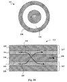
- FIG. 6A is a schematic diagram of a PQSL apparatus 600 according to an embodiment of the invention.
- a beam of pumping radiation 601 is incident on a thin piece of neodymium-doped laser material 602 .
- the laser material 602 has a first-surface 603 configured, e.g., with a suitable coating, such that the first surface 603 acts both to transmit the pump light and to create a resonant cavity for the PQSL apparatus 600 .
- the configuration or coating of the first surface 603 affects the output coupling of the laser apparatus 600 .
- a second surface 604 of the laser material 602 is configured (e.g., coated) to provide a low-loss anti-reflection coating at the 914-nm wavelength of the PQSL apparatus 600 .
- a passive Q-switch 605 is optically coupled to the laser material 602 proximate the second surface 604 .
- a coated semiconductor may act as the passive Q-switch 605 .
- the second surface 604 and the Q-switch 605 are separated by a narrow gap G.
- the coating on the first surface 603 and the coated semiconductor Q-switch 605 respectively act as the first and second reflecting surfaces of a resonant cavity 606 .
- the neodymium-doped laser material 602 is neodymium-doped Yttrium Vanadate (Nd:YVO 4 ).
- the neodymium-doped laser material 602 may be another material such as Neodymium-doped Gadolinium Orthovanadate, (Nd:GdVO 4 ), Neodymium-doped Yttrium Lithium Fluoride (Nd:YLF), or Neodymium-doped Yttrium Aluminum Garnet Nd:YAG.
- FIG. 6B shows a schematic diagram of the PQSL apparatus 600 with additional structure that may be associated with the thin piece of laser material.
- the laser material 602 may be bonded with a transparent adhesive 607 to a mounting block 608 , which may be a thicker piece of transparent, high thermal conductivity material such as sapphire, silicon carbide, or yttrium aluminum garnet.
- the mounting block 608 provides structural support to the laser material 602 if it is very thin, and also allows heat to be transported from the laser material 602 .
- Any coating on the first-surface 603 of the laser material 602 , which is in contact with the adhesive, 607 should be designed with the index of refraction of the adhesive 607 taken into account. In addition, it is desirable that the adhesive 607 be heat-resistant.
- the function of the Q-switch 605 is to provide an amount of loss that keeps the PQSL apparatus 600 from lasing most of the time, but which disappears once the PQSL apparatus 600 begins to lase, so that the PQSL can efficiently emit a powerful pulse after the loss is “saturated.” Once the pulse is emitted, the Q-switch 605 returns to its lossy state.
- FIG. 7 shows a possible design for the semiconductor passive Q-switch 605 .
- the Q-switch 700 depicted in FIG. 7 is of a type known as a Semiconductor Bragg Reflector (SBR) or as a Semiconductor Saturable Absorber Mirror (SESAM).
- a substrate 702 serves as a support for epitaxial semiconductor layers 704 .
- the substrate 702 may be a bulk semiconductor material e.g. Gallium Arsenide (GaAs).
- the epitaxial semiconductor layers 704 are generally compatible with semiconductor growth processes.
- the epitaxial semiconductor layers 704 include a semiconductor mirror stack 706 , and quantum well stack 708 .
- the epitaxial semiconductor layers 704 may also include a buffer layer between the substrate 702 and the semiconductor mirror stack 706 .
- the semiconductor mirror stack 706 contains alternating high and low refractive index layers.
- the high refractive index layers may be epitaxial layers of Al x Ga 1 ⁇ x As (where x is between 0 and about 0.1).
- the low refractive index layers may be epitaxial layers of Al y Ga 1 ⁇ y As (where y is between about 0.9 and 1).
- Each of the high and low refractive index layers in the semiconductor mirror stack 706 has an optical thickness of about one-quarter of the wavelength of the laser radiation.
- the alternating high and low refractive index layers in the semiconductor mirror stack 706 create a highly reflective structure at the lasing wavelength.
- the quantum well stack 708 can contain between about 3 and about 15 quantum wells.
- the quantum well stack 708 creates a loss at the wavelength of the laser radiation when low levels of laser radiation are present, but this loss greatly decreases, or “saturates,” when high levels of light are present.
- the optical thickness of the quantum well stack 708 is generally an odd multiple of one-quarter wavelength ( ⁇ /4) of the laser radiation to achieve anti-resonance and insensitivity to layer thickness.
- a dielectric overcoat 710 serves to reflect as much as possible of the pump light, so that the pump light does not enter and saturate the quantum wells, and also reflects a chosen amount at the lasing wavelength, in order to keep the amount of lasing light in the quantum well to a desirable level that will not damage the semiconductor.
- the dielectric overcoat 710 generally has a reflectivity R that is greater than about 90% at the pump wavelength.
- the SBR itself used in the Q-switch 700 may be based on a substrate of n-type GaAs. Layers of other semiconductors are grown on the substrate.
- the semiconductor mirror stack 706 may include 60 layers consisting of 30 layer pairs of GaAs and AlAs, with each layer having an optical thickness of 1 ⁇ 4 wave for laser radiation at a vacuum wavelength, e.g., of 914 nm.
- the quantum well stack 708 may have between 3 and 15 quantum wells (e.g., 9 to 12) with each quantum well made from a layer of absorbing material such as Indium Gallium Arsenide (InGaAs).
- Each quantum well is sandwiched between layers of non-absorbing material such as Gallium Arsenide Phosphide (GaAsP).
- GaAsP Gallium Arsenide Phosphide
- the stoichiometric ratios of In, Ga, As, and P in these layers were GaAs 0.8 P 0.2 and In 0.3 Ga 0.7 As respectively.
- the thickness of the InGaAs quantum-well layer was chosen to create photoluminescence at a vacuum wavelength of 930 nm ⁇ 15 nm, and the thickness of the GaAsP was chosen to balance the strain between the absorbing quantum well layers and the non-absorbing barrier layers.
- the quantum well stack 708 may include one or more spacer layers of GaAs or InGaP to adjust the overall thickness of the quantum well stack 708 to an odd number of one-quarter wavelengths ( ⁇ /4) for radiation at a vacuum wavelength ⁇ of 914 nm.
- Each spacer layer can be placed between two barrier layers. If InGaP is used as a spacer material, the composition must be chosen so that the lattice of the InGaP matches that of GaAs, which requires 49% In and 51% P.
- the dielectric overcoat 710 above the epitaxial semiconductor layers 704 may include alternating layers of SiO 2 and HfO 2 .
- the dielectric overcoat 710 can have between 87% and 96% reflectivity for the laser radiation, (e.g., at 914 nm vacuum wavelength) and >90% reflectivity for the pump radiation (e.g., at a vacuum wavelength of 809 nm).
- FIG. 8 shows the overall structure of a PQSL 800 that incorporates apparatus of the type described in FIGS. 6A–6B and FIG. 7 .
- the PQSL 800 generally includes a PQSL apparatus 801 , like the PQSL apparatus 600 described above, having a laser material 802 , and a Q-switch 804 .
- the PQSL 800 further includes a laser diode 812 , a fast axis collection lens 806 , a collimating lens 808 , and a focusing lens 810 .
- a beamsplitter 814 may be disposed between collimating lens 808 and the focusing lens 810 .
- the laser diode 812 provides pump power in the form of pumping radiation 811 for the PQSL apparatus 801 .
- the wavelength of pump radiation 811 from the laser diode 812 is typically about 810 nm.
- the laser diode 812 may be a Model S-81-650C-50-C, with fiber lens, produced by Coherent Inc, of Santa Clara Calif. This particular laser diode puts out 0.65 Watts from a 0.05 mm aperture, and is collimated in one dimension by a cylinder lens attached by the manufacturer, which may serve as lens 806 .
- increasing the pump power increases the repetition rate. Repetition rates of 3 MHz have been achieved in embodiments of the present invention and higher repetition rates are believed to be achievable with higher power pump sources.
- the laser material 802 may be of the type described above with respect to laser material 602 including first and second surface coatings as described above.
- the laser material 802 may be Neodymium-doped Yttrium Orthovanadate (Nd:YVO 4 ), which is available from Castech, of Fujian, China, e.g., in 3 mm ⁇ 4 mm ⁇ 1 mm pieces, with the unique “c” axis parallel to the 4 mm axis.
- An output coupler may be coated onto the 3 mm ⁇ 4 mm surface. The output coupler coating may be specified for 1% transmission at 914 nm and 95% transmission at 809 nm.
- the Nd:YVO 4 part may be bonded to a sapphire carrier, and thinned down to 0.075 mm using standard grinding and polishing techniques. Then the polished surface may be anti-reflection coated for reflection less then 0.25% at 914 nm.
- the AR coating can be optimized for either of the two polarizations, and it is better if it is optimized for the same polarization that has the lowest output coupling. Both coatings on the Nd:YVO 4 may be subject to very high pulsed intensity, and the coating design must be chosen for high damage threshold.
- the Nd:YVO 4 piece may be bonded to a piece of sapphire for purposes of handling and heat removal.
- the Sapphire may be 1 mm thick, and oriented so that it will not significantly affect the polarization of the output of the laser.
- the sapphire is available from Esco products of Oak Ridge, N.J.
- the two parts may be bonded together with clear optical epoxy, such as Epotek 301, available from Epoxy Technology of Billerica, Mass.
- the surface of the Sapphire facing away from the Nd:YVO 4 (toward the laser diode 812 ) may be anti-reflection coated for the pump and lasing wavelengths.
- the other surface (the one with the epoxy) may be uncoated.
- Lenses 806 , 808 , 810 collect the pump radiation from the diode 812 and focus it onto the laser material 802 .
- the fast-axis collecting lens 806 is used when necessary to compensate for differing rates of divergence of the pump radiation as it emerges from the diode 812 .
- the pump radiation diverges more rapidly along a fast axis than along a slow axis.
- the fast-axis collecting lens 806 reduces the divergence along the fast axis so that the beam of pump radiation diverges more uniformly.
- the fast-axis collecting lens 806 can be a fiber lens, or other lens with cylindrical symmetry, with an axis of cylindrical symmetry oriented perpendicular to the fast axis.
- the collimating lens 808 may be a model 350170-B from Lightpath Technologies of Orlando, Fl.
- This particular model of lens is a molded glass aspheric lens with a focal length of 6.16 mm and a N.A. of 0.30.
- the collimating lens 808 may be AR coated over the wavelength range 600 nm to 1050 nm.
- the focusing lens 810 may be a model 350150 from Lightpath Technologies of Orlando, Fl.
- This particular model of lens is a molded glass aspheric lens with a focal length of 2 mm and a N.A. of 0.50.
- the focusing lens 810 may be AR coated for ⁇ 0.25% reflectivity at 914 nm.
- the Q-switch 804 may be a SBR of the type described with respect to FIG. 7 .
- the laser material 802 and the Q-switch 804 may be supported by a thermally-controlled structure 816 .
- the structure 816 can expand or contract enough to adjust the laser resonator round trip length over more than one wavelength of the lasing radiation, allowing tuning of the laser wavelength to the point most likely to give powerful, single-frequency laser output.
- the PQSL apparatus 801 generates laser output radiation 815 from the pumping radiation 811 as described above.
- the beamsplitter 814 transmits the pumping radiation 811 from the laser diode 812 , while reflecting the laser output radiation 815 from the PQSL apparatus 801 away from the laser diode 812 so that laser output radiation 815 can exit the laser as a usable beam.
- the beamsplitter 814 may be a plano/plano optic designed for >95% transmission at 809 nm and greater than 95% reflection at 914 nm, at 45° incidence, for both polarizations of both the pumping radiation 811 and the laser output radiation 815 .
- the beamsplitter 814 may be coated using standard coating techniques such as sputtering, vapor deposition and the like.
- FIG. 8 uses the beamsplitter 814 since the same surface of the laser material 802 serves as both an input coupler for the pumping radiation 811 and output coupler for the laser output radiation 815 .
- Alternative embodiments of the present invention can avoid the use of a beamsplitter, e.g., if the Q-switch 804 is configured to also serve as an output coupler for the laser output radiation.
- All optical components may be mounted using side-mount blocks. Side mounting is described in detail in commonly assigned U.S. Pat. Nos. 6,320,706 and 6,366,593, both of which are incorporated herein by reference.
- the Q-switch 804 e.g., an SBR
- the Q-switch 804 may be aligned parallel to the laser material 802 (e.g., Nd:YVO 4 ,) with an air gap of less than 0.01 mm.
- Both the laser material 802 and Q-switch 804 may be mounted to the thermally controlled structure 816 , e.g., an aluminum plate.
- the separation between the mounting points may be about 3 mm. This is enough distance that thermal expansion can be used to adjust the separation of the Q-switch 804 from the lasing material 802 by 1 or 2 microns with a temperature change of 20° or 30° C.
- a small thermo-electric cooler may control the temperature of the aluminum plate.
- the basic PQSL design of FIGS. 6A–6B , 7 and 8 has features in common with conventional structures used previously to build PQSLs at the more commonly used and more easily optimized wavelength of 1064 nm. However, a multi-parameter optimization is needed to make the PQSL 800 of FIG. 8 operate as a useful 914 nm PQSL.
- a desirable PQSL for use in the laser 200 or display system 500 would preferably produce radiation at a wavelength of about 914-nm (corresponding to an electronic transition from the 4 F 3/2 level to the 4 I 9/2 level in Neodymium) in the form of pulses less than about 1.5 nsec in pulse length and greater than about 100 kHz in repetition rate. Table I lists the parameters which were studied and optimized.
- Neodymium concentration in the laser material measured in % Thickness of the laser material, measured in millimeters Transmission of the first surface of the laser material at 914 nm, measured in % Polarization selectivity of the coating on the first surface of the laser material
- Intensity of pump radiation in the laser material measured in Watts/mm 2 Semiconductor material for the substrate of the SBR Semiconductor material of the high/low index layers of the semiconductor mirror Semiconductor material for the quantum wells and for the material between them
- Number of quantum wells in the SBR Reflectivity of the dielectric overcoating at the pump & laser wavelength measured in %
- Nd:YVO 4 was used as the laser material.
- the laser material 602 (e.g., Nd:YVO 4 ) is made very thin in order to provide short, single-frequency pulses.
- the primary disadvantage of using very thin pieces is that absorption of the pump light decreases. This can be shown very simply from theory.
- the obvious way to increase pump absorption is to increase the concentration of Neodymium (Nd).
- Nd:YVO 4 is commercially available with Nd concentrations ranging from about 0.25% to about 3%.
- the doping concentration must be between 1% and 3% as measured in fractional substitution of Yttrium by Neodymium.
- Nd:YVO 4 this is equivalent to a concentration of Nd of between about 1.3 ⁇ 10 17 atoms per mm 3 and 3.8 ⁇ 10 17 atoms per mm 3 .
- a Nd concentration of about 2% works particularly well.
- the thickness of the laser material is a critical parameter. There are two reasons to make the laser material 602 very thin. First, the pulses get shorter when the part gets thinner. Second, the PQSL will oscillate in a single frequency only if the resonator is so short that it supports only one mode of oscillation. The length of the resonator cavity is almost totally determined by the thickness of the laser material 602 , since the Q-switch 605 and the air gap provide negligible thickness. As the laser material 602 gets too thin, however, pump absorption gets so small that the PQSL apparatus 600 is not useful. Usually, it is desired to absorb as much pump radiation as possible.
- the inventors have determined that a PQSL can operate effectively with the desired pulse length even if the lasing material 602 is so thin that it absorbs less than half of the pump radiation.
- the thickness of Nd:YVO 4 needs to be less than 0.1 mm in order to have a useful single-frequency PQSL at the desired pulse length of less than 1.5 nsec.
- the inventors obtained their best results at a thickness of about 0.075 mm.
- useful PQSLs were made with parts as thin as 0.056 mm, a minimum thickness was not experimentally determined, but it is presumably greater than zero.
- Two opposite forces drive the choice of the transmission of the first surface 603 of the lasing material 602 at the lasing wavelength of about 914 nm, also known as the output coupling of the PQSL apparatus 600 .
- a very low output coupling transmission is desirable in order to lower the threshold of lasing, so that the apparatus 600 will oscillate when pumped by available pump lasers.
- low output couplings will lead to a greater chance of optical damage in the laser, because the lasing light is trapped inside the resonator, which leads to higher levels of internally circulating power for a given level of output power.
- Such high internal circulating power levels can lead to serious problems of optical damage to both to the AR-coated second surface 604 of the laser material 602 and to the Q-switch 605 .
- the inventors determined that to achieve lasing at all, the output coupling had to be below about 2%. At levels of about 0.5% and below serious problems of optical damage occurred. The best performance was achieved at about 1% output coupling.
- a single polarization is desirable for frequency doubling of the laser output of the PQSL apparatus 600 .
- the inventors have determined that it is possible to cause the PQSL apparatus 600 to lase in a single polarization by designing the output coupling so that there is slightly lower transmission for one polarization than for the other. Specifically, the polarization with the lower output coupling will lase.
- the inventors built a PQSL apparatus with output coupling of 0.94% for the ordinary polarization, and 0.98% for the extraordinary polarization. Only the ordinary polarization oscillated. Suitable coatings are available from MLD Optical Coatings of Mountain View, Calif. It is believed that for consistent single-polarization lasing, it is desirable to design coatings with the transmission split as much as possible. Fortunately, the high birefringence of Nd:YVO 4 makes it possible to design coatings with significant polarizing properties.
- the power in the pump beam divided by its cross-sectional area at the Nd:YVO 4 crystal is known as the pump intensity.
- Very high pump intensities are required even to get lasing at 914 nm, and even higher intensity is needed to achieve high repetition rate and short pulses.
- High pump intensity can be accomplished by using a laser diode pump source with high power output per unit length of the emitting aperture. High quality lenses may be used to focus the pump beam into a small spot. The desired performance could be obtained by focusing a 0.5-Watt pump beam into a circular area of radius about 0.02 mm.
- the pump intensity of such a system is typically greater than about 400 Watts/mm 2 .
- GaAs Gallium Arsenide
- SBR Gallium Arsenide
- layer 702 of FIG. 7 the substrate material of the SBR, e.g., layer 702 of FIG. 7 .
- GaAs is poorly transmitting at 914 nm, which is why the first surface of the laser material was used as the output coupler.
- GaAs is a standard substrate for all of the ternary (three-element) materials that are used in the SBR design described above with respect to FIG. 7 .
- the semiconductor mirror stack 706 of alternating high and low refractive index layers of FIG. 7 .
- GaAs followed by either AlAs or GaAlAs was used.
- Each layer had an optical thickness of 1 ⁇ 4 wave at the laser wavelength of 914 nm, so that the stack as a whole is highly reflecting at 914 nm. It was determined that 30 layer pairs were sufficient to achieve >99% reflectivity of the stack.
- the quantum well stack 708 was fabricated in the form of layers of In 0.3 Ga 0.7 As sandwiched between layers of GaAs 0.8 P 0.2 . Spacer layers were added to adjust the location of the quantum wells relative to the standing wave pattern. It is usually desirable to have the quantum wells located where the intensity of the standing wave pattern is a maximum. The spacer layers also adjust the overall optical thickness of the quantum well stack 708 . The optical thickness of this structure as a whole is chosen to be an odd-integer number of quarter waves at 914 nm vacuum wavelength.
- the In 0.3 Ga 0.7 As layers are known as “quantum wells” because their extreme thinness causes them to manifest quantum mechanical properties.
- the composition and thickness of these layers were chosen so that they have a photoluminescence peak at 930 nm ⁇ 15 nm.
- the quantum wells provide the saturable absorption. These quantum wells absorb 914 nm light, creating loss at 914 nm which can raise the lasing threshold of the laser. Once lasing begins, the quantum wells absorb some of the 914 nm light and go into a non-absorbing state, that is, they are “saturated.” At this point the laser suddenly finds itself well above threshold, since the loss disappears. The circulating optical power grows very quickly into a powerful Q-switched pulse.
- the GaAs 0.8 P 0.2 material has 2 purposes. First, it fills up space to separate the quantum wells and to keep the entire structure at an optical thickness of an odd multiple of one quarter of the wavelength of the laser output radiation. Second, it “strain balances” the In 0.3 Ga 0.7 As. This means that the tensile/compressive forces of a layer of one material are equal and opposite that to the other layer, so that no net strain builds up that could disrupt the epitaxial growth process.
- Spuhler et. al. describe how the repetition rate and pulse duration of the PQSL are determined by a quantity called q 0 , which is the amount of saturable loss measured in per cent. A higher value of q 0 will lead to shorter pulses and lower repetition rate. For a given pulse length and repetition rate, one can use the Spuhler theory to quickly determine what value of q 0 is desired. However, knowing the desired value of q 0 by itself does not allow one to directly design the laser.
- the saturable loss parameter q 0 is a complicated function of the number of quantum wells, the exact position of each quantum well, and the reflectivity of the dielectric overcoating.
- the dielectric overcoating 710 of FIG. 7 has 2 purposes. First, it serves to exclude 809 nm pump light from the semiconductor layers below it. Due to the small thickness of the laser material, about 50% of the pump light is transmitted all the way through the laser material and is incident on the SBR. This pump light could saturate the quantum wells 708 and reduce the effective value of q 0 in a large and unpredictable way.
- the second purpose is to reduce the amount of Q-switched laser light in the semiconductor part of the Q-switch, in order to reduce damage due to high optical power.
- Most of the light in the air gap between the laser material and the Q-switch is reflected by the dielectric overcoating 710 , and only a fraction enters the epitaxial semiconductor layers 704 . This keeps the intensity in the epitaxial semiconductor layers 704 below the threshold for damage.
- the reduction in light in the semiconductor reduces the loss due to the quantum wells 708 , since they see less light. Thus a larger number of quantum wells 708 are needed to get to the same level of q 0 .
- a reflectivity of the dielectric stack at 914 nm between about 87% and about 96% was used.
- the net value of q 0 typically used was between about 0.2% and about 0.5%.
- FIG. 9 shows an oscillograph of a pulse from the PQSL, with a pulse length ⁇ t of 1.32 nsec.
- FIG. 10 shows a graph of the power and repetition rate of a PQSL laser of the type depicted in FIG. 8 as a function of the current supplied to the pump diode. Over a wide range of pump currents the repetition rate exceeded the initial goal of 1 MHz.
- the wavelength may vary depending on parameters such as temperature.
- FIG. 11 shows the tuning of the laser caused by changing the temperature of the resonator platform.
- the different lines correspond to different modes of the laser.
- the laser supports more than one mode.
- the atomic transition from the 4 F 3/2 level to the 4 I 9/2 level of Neodymium in other Neodymium-doped lasing materials may produce laser radiation at wavelengths other than 914 nm.
- the scope of the invention is not limited to the 914-nm wavelength of the laser radiation.
- Embodiments of the present invention that utilize fiber amplifiers can be much more efficient than competing techniques, since fiber amplifiers are very efficient. Temperature of pump diodes can be less critical since fiber amplifiers have loose tolerances on pump wavelength. The embodiments of the present invention can be implemented without water cooling since the more efficient system dissipates less heat and the tolerant pump wavelength specification generally requires less precise temperature control. Furthermore, fiber based systems can be made more compact since fiber can be wound up into a small volume.
- applications of the PQSL apparatus described above are not limited to sources of blue light and color display systems.
- Another set of applications is in lasers used for fluorescence excitation.
- a high repetition rate is needed so that the light appears to be continuous on the time scale of the measurement process.
- Many other applications need blue light that is either continuous or which is at such a high repetition rate that it appears to be continuous.
- a 914 nm pulsed laser, with a high repetition rate but with pulses of less than 2 nsec duration, is a key component in such a blue system.
- Another application is in laser radar systems.
Abstract
Description
where rpc represents some distance from the axis of the fiber that lies within the pump cladding and A represents a cross sectional area of the fiber within rpc of the axis. For example, if the fiber has a circular cross section, A=πrpc 2. The radius rpc is typically greater than a few undesired wavelengths.
| TABLE I |
| Optimized Parameters |
| Neodymium concentration in the laser material, measured in % |
| Thickness of the laser material, measured in millimeters |
| Transmission of the first surface of the laser material at 914 nm, measured |
| in % |
| Polarization selectivity of the coating on the first surface of the laser |
| material |
| Intensity of pump radiation in the laser material, measured in Watts/mm2 |
| Semiconductor material for the substrate of the SBR |
| Semiconductor material of the high/low index layers of the semiconductor |
| mirror |
| Semiconductor material for the quantum wells and for the material |
| between them |
| Number of quantum wells in the SBR |
| Reflectivity of the dielectric overcoating at the pump & laser wavelength, |
| measured in % |
Claims (20)
Priority Applications (1)
| Application Number | Priority Date | Filing Date | Title |
|---|---|---|---|
| US10/662,086 US7116687B2 (en) | 2003-09-12 | 2003-09-12 | High repetition rate passively Q-switched laser for blue laser based on interactions in fiber |
Applications Claiming Priority (1)
| Application Number | Priority Date | Filing Date | Title |
|---|---|---|---|
| US10/662,086 US7116687B2 (en) | 2003-09-12 | 2003-09-12 | High repetition rate passively Q-switched laser for blue laser based on interactions in fiber |
Publications (2)
| Publication Number | Publication Date |
|---|---|
| US20050058163A1 US20050058163A1 (en) | 2005-03-17 |
| US7116687B2 true US7116687B2 (en) | 2006-10-03 |
Family
ID=34274025
Family Applications (1)
| Application Number | Title | Priority Date | Filing Date |
|---|---|---|---|
| US10/662,086 Expired - Lifetime US7116687B2 (en) | 2003-09-12 | 2003-09-12 | High repetition rate passively Q-switched laser for blue laser based on interactions in fiber |
Country Status (1)
| Country | Link |
|---|---|
| US (1) | US7116687B2 (en) |
Cited By (1)
| Publication number | Priority date | Publication date | Assignee | Title |
|---|---|---|---|---|
| US20140286362A1 (en) * | 2013-03-22 | 2014-09-25 | Ipg Photonics Corporation | High Power Neodymium Fiber Lasers and Amplifiers |
Families Citing this family (9)
| Publication number | Priority date | Publication date | Assignee | Title |
|---|---|---|---|---|
| JP2006189587A (en) * | 2005-01-05 | 2006-07-20 | Nidek Co Ltd | Medical laser apparatus |
| US20100301237A1 (en) * | 2009-05-28 | 2010-12-02 | International Technology Group | Method and apparatus for production of heat and/or magnetic field through photon, positron or particle infusion |
| CN102723659B (en) * | 2012-05-02 | 2014-05-07 | 清华大学 | Method for generation of long-span repetition frequency jumping Q-switched laser pulses |
| CN102723660B (en) * | 2012-05-02 | 2014-11-26 | 清华大学 | Electro-optic Q-switched pulse laser device with repeat frequency being variable in wide range |
| FR3024633B1 (en) * | 2014-07-30 | 2016-07-29 | Onera (Office Nat D'etudes Et De Rech Aerospatiales) | LASER SOURCE, APPARATUS AND METHOD FOR INTERACTING SIMULTANEOUSLY WITH MULTIPLE ATOMIC SPECIES |
| WO2018217184A1 (en) | 2017-05-20 | 2018-11-29 | Sandstone Diagnostics, Inc. | Specimen cup |
| USD867611S1 (en) | 2018-01-29 | 2019-11-19 | Sandstone Diagnostics, Inc. | Sample cup |
| CN115213408A (en) * | 2021-04-21 | 2022-10-21 | 深圳市联赢激光股份有限公司 | Additive manufacturing process, additive layer, additive product and composite laser |
| CN113725712B (en) * | 2021-08-26 | 2022-12-30 | 中国人民解放军国防科技大学 | System and method for generating pulse blue laser based on alkali metal vapor and neodymium-doped solid |
Citations (64)
| Publication number | Priority date | Publication date | Assignee | Title |
|---|---|---|---|---|
| US4708421A (en) | 1985-02-08 | 1987-11-24 | The Board Of Trustees Of The Leland Stanford Junior University | In-line fiber optic memory |
| US4734911A (en) | 1986-03-14 | 1988-03-29 | Hughes Aircraft Company | Efficient phase conjugate laser |
| US4796262A (en) | 1985-03-18 | 1989-01-03 | Selenia Industrie Elettroniche Associate Spa | Optical resonator using a passive Q switch or other optical element with low-damage threshold |
| US4815804A (en) | 1985-02-08 | 1989-03-28 | The Board Of Trustees Of The Leland Stanford Junior University | In-line fiber optic memory and method of using same |
| US4952059A (en) | 1986-06-06 | 1990-08-28 | The Board Of Trustees Of The Leland Stanford Junior University | Reentrant fiber raman gyroscope |
| US5162940A (en) | 1987-03-06 | 1992-11-10 | The United States Of America As Represented By The Secretary Of The Air Force | Multiple energy level, multiple pulse rate laser source |
| US5200964A (en) | 1991-03-12 | 1993-04-06 | General Instrument Corporation | Broad linewidth lasers for optical fiber communication systems |
| US5239408A (en) | 1992-01-21 | 1993-08-24 | Regents Of The University Of California | High power, high beam quality regenerative amplifier |
| US5295209A (en) | 1991-03-12 | 1994-03-15 | General Instrument Corporation | Spontaneous emission source having high spectral density at a desired wavelength |
| US5388114A (en) | 1994-03-17 | 1995-02-07 | Polaroid Corporation | Miniaturized self-Q-switched frequency-doubled laser |
| US5400165A (en) | 1993-09-10 | 1995-03-21 | At&T Corp. | Optical communication using dispersion-induced FM to AM conversion with nonlinearity-induced stabilization |
| US5434875A (en) | 1994-08-24 | 1995-07-18 | Tamar Technology Co. | Low cost, high average power, high brightness solid state laser |
| US5461637A (en) | 1994-03-16 | 1995-10-24 | Micracor, Inc. | High brightness, vertical cavity semiconductor lasers |
| US5491707A (en) | 1994-08-24 | 1996-02-13 | Jamar Technologies Co. | Low cost, high average power, high brightness solid state laser |
| US5511085A (en) | 1994-09-02 | 1996-04-23 | Light Solutions Corporation | Passively stabilized intracavity doubling laser |
| US5539765A (en) | 1994-03-03 | 1996-07-23 | The University Court Of The University Of St. Andrews | High efficiency laser |
| US5541947A (en) | 1995-05-10 | 1996-07-30 | The Regents Of The University Of Michigan | Selectively triggered, high contrast laser |
| US5648976A (en) | 1994-04-27 | 1997-07-15 | The United States Of America As Represented By The Secretary Of The Air Force | Laser with variable pulse length |
| US5675596A (en) | 1995-02-25 | 1997-10-07 | Korea Advanced Institute Of Science And Technology | Passively Q-switched laser with a dual-cavity configuration |
| US5680412A (en) | 1995-07-26 | 1997-10-21 | Demaria Electrooptics Systems, Inc. | Apparatus for improving the optical intensity induced damage limit of optical quality crystals |
| US5689363A (en) | 1995-06-12 | 1997-11-18 | The Regents Of The University Of California | Long-pulse-width narrow-bandwidth solid state laser |
| US5740190A (en) * | 1996-05-23 | 1998-04-14 | Schwartz Electro-Optics, Inc. | Three-color coherent light system |
| US5751751A (en) | 1993-08-26 | 1998-05-12 | Laser Power Corporation | Deep blue microlaser |
| US5761227A (en) * | 1994-08-23 | 1998-06-02 | Laser Power Corporation | Efficient frequency-converted laser |
| US5768302A (en) | 1996-02-01 | 1998-06-16 | Lightwave Electronics Corporation | Multi quasi phase matched interactions in a non-linear crystal and method using same |
| US5790574A (en) | 1994-08-24 | 1998-08-04 | Imar Technology Company | Low cost, high average power, high brightness solid state laser |
| US5790584A (en) | 1995-07-28 | 1998-08-04 | Korea Advanced Institute Of Science And Technology | Highly repetitive laser employing a rotating wedge |
| US5825465A (en) | 1996-07-23 | 1998-10-20 | Commissariat A L'energie Atomique | Autodyne detection laser velocimeter |
| US5889798A (en) | 1995-01-24 | 1999-03-30 | Commissariat A L'energie Atomique | Active-switching laser and microchip laser |
| US5920588A (en) | 1996-04-11 | 1999-07-06 | Fujitsu Limited | Method and device for generation of phase conjugate light and wavelength conversion, and system having the device |
| US5982482A (en) | 1997-07-31 | 1999-11-09 | Massachusetts Institute Of Technology | Determining the presence of defects in thin film structures |
| US5982789A (en) | 1995-11-22 | 1999-11-09 | Light Solutions Corporation | Pulsed laser with passive stabilization |
| US5986234A (en) | 1997-03-28 | 1999-11-16 | The Regents Of The University Of California | High removal rate laser-based coating removal system |
| US6026102A (en) | 1997-04-21 | 2000-02-15 | Shimoji; Yukata | Multi element single mode microchip lasers |
| US6061378A (en) | 1997-05-13 | 2000-05-09 | Cutting Edge Optronics, Inc. | Multiple resonant cavity solid-state laser |
| US6096496A (en) | 1997-06-19 | 2000-08-01 | Frankel; Robert D. | Supports incorporating vertical cavity emitting lasers and tracking apparatus for use in combinatorial synthesis |
| US6100516A (en) | 1996-10-14 | 2000-08-08 | Commissariat A L'eneriqie Atomigue | Velocity measurement device and laser range finder using a coherent detection |
| US6141143A (en) | 1998-05-01 | 2000-10-31 | Light Solutions Corporation | CW laser amplifier |
| US6195369B1 (en) | 1995-12-22 | 2001-02-27 | Scientific-Atlanta, Inc. | High stability soliton source |
| US6208458B1 (en) | 1997-03-21 | 2001-03-27 | Imra America, Inc. | Quasi-phase-matched parametric chirped pulse amplification systems |
| US20010017724A1 (en) | 2000-02-28 | 2001-08-30 | Yutaka Miyamoto | Optical transmission method, optical tramsmitter, optical receiver, and optical transmission system |
| US20010021288A1 (en) | 2000-03-03 | 2001-09-13 | Shigeki Watanabe | Method, device, and system for waveform shaping of signal light |
| US6301275B2 (en) | 1999-02-02 | 2001-10-09 | University Of Central Florida | Self-frequency doubled Nd-doped YCOB laser |
| US6307984B1 (en) | 1996-08-22 | 2001-10-23 | Fujitsu Limited | Optical fiber communication system using optical phase conjugation as well as apparatus applicable to the system and method of producing the same |
| US6356578B1 (en) * | 1999-12-29 | 2002-03-12 | Photonics Industries International, Inc. | Attenuator |
| US6393035B1 (en) | 1999-02-01 | 2002-05-21 | Gigatera Ag | High-repetition rate passively mode-locked solid-state laser |
| US6424773B1 (en) | 1998-06-23 | 2002-07-23 | Fujitsu Limited | Optical gate device, manufacturing method for the device, and system including the device |
| US6445494B1 (en) | 1996-12-04 | 2002-09-03 | Southampton Photonics Limited | Optical amplifier and light source |
| US6449408B1 (en) | 1997-10-17 | 2002-09-10 | Corning Incorporated | Soliton pulse generator |
| US20020136246A1 (en) | 2001-03-16 | 2002-09-26 | Sony Corporation | Laser apparatus |
| US20030031411A1 (en) | 2001-08-10 | 2003-02-13 | Arbore Mark A. | Solid state laser generating UV radiation for writing fiber bragg gratings |
| US20030031215A1 (en) | 2001-08-10 | 2003-02-13 | Kane Thomas J. | Compound light source employing passive Q-switching and nonlinear frequency conversion |
| US20030030756A1 (en) | 2001-08-10 | 2003-02-13 | Kane Thomas J. | Pulse sequencing for generating a color image in laser-based display systems |
| US20030058904A1 (en) | 2001-09-24 | 2003-03-27 | Gigatera Ag | Pulse-generating laser |
| US6542228B1 (en) | 1997-01-08 | 2003-04-01 | York Sensors Limited | Optical time domain reflectometry method and apparatus |
| US20030063860A1 (en) | 2001-09-28 | 2003-04-03 | Fujitsu Limited | Method, device, and system for waveform shaping of signal light |
| US20030063884A1 (en) | 2001-01-04 | 2003-04-03 | Smith Duane D. | Power scalable optical systems for generating, transporting, and delivering high power, high quality, laser beams |
| US6563995B2 (en) | 2001-04-02 | 2003-05-13 | Lightwave Electronics | Optical wavelength filtering apparatus with depressed-index claddings |
| US6577429B1 (en) | 2002-01-15 | 2003-06-10 | Eastman Kodak Company | Laser projection display system |
| US20030118060A1 (en) * | 2001-09-24 | 2003-06-26 | Gigatera Ag | Pulse-generating laser |
| US6614975B2 (en) | 1998-07-03 | 2003-09-02 | University Of Southampton | Optical fiber and optical fiber device |
| US6614815B1 (en) | 2000-06-29 | 2003-09-02 | Lightwave Electronics | Blue laser based on interactions in fiber |
| US6735234B1 (en) * | 2000-02-11 | 2004-05-11 | Giga Tera Ag | Passively mode-locked optically pumped semiconductor external-cavity surface-emitting laser |
| US6826219B2 (en) * | 2002-03-14 | 2004-11-30 | Gigatera Ag | Semiconductor saturable absorber device, and laser |
-
2003
- 2003-09-12 US US10/662,086 patent/US7116687B2/en not_active Expired - Lifetime
Patent Citations (71)
| Publication number | Priority date | Publication date | Assignee | Title |
|---|---|---|---|---|
| US4815804A (en) | 1985-02-08 | 1989-03-28 | The Board Of Trustees Of The Leland Stanford Junior University | In-line fiber optic memory and method of using same |
| US4708421A (en) | 1985-02-08 | 1987-11-24 | The Board Of Trustees Of The Leland Stanford Junior University | In-line fiber optic memory |
| US4796262A (en) | 1985-03-18 | 1989-01-03 | Selenia Industrie Elettroniche Associate Spa | Optical resonator using a passive Q switch or other optical element with low-damage threshold |
| US4734911A (en) | 1986-03-14 | 1988-03-29 | Hughes Aircraft Company | Efficient phase conjugate laser |
| US4952059A (en) | 1986-06-06 | 1990-08-28 | The Board Of Trustees Of The Leland Stanford Junior University | Reentrant fiber raman gyroscope |
| US5162940A (en) | 1987-03-06 | 1992-11-10 | The United States Of America As Represented By The Secretary Of The Air Force | Multiple energy level, multiple pulse rate laser source |
| US5200964A (en) | 1991-03-12 | 1993-04-06 | General Instrument Corporation | Broad linewidth lasers for optical fiber communication systems |
| US5295209A (en) | 1991-03-12 | 1994-03-15 | General Instrument Corporation | Spontaneous emission source having high spectral density at a desired wavelength |
| US5239408A (en) | 1992-01-21 | 1993-08-24 | Regents Of The University Of California | High power, high beam quality regenerative amplifier |
| US5751751A (en) | 1993-08-26 | 1998-05-12 | Laser Power Corporation | Deep blue microlaser |
| US5400165A (en) | 1993-09-10 | 1995-03-21 | At&T Corp. | Optical communication using dispersion-induced FM to AM conversion with nonlinearity-induced stabilization |
| US5539765A (en) | 1994-03-03 | 1996-07-23 | The University Court Of The University Of St. Andrews | High efficiency laser |
| US5461637A (en) | 1994-03-16 | 1995-10-24 | Micracor, Inc. | High brightness, vertical cavity semiconductor lasers |
| US5627853A (en) | 1994-03-16 | 1997-05-06 | Coherent, Inc. | Optimized laser energy conversion through automatic mode matched pumping |
| US5388114A (en) | 1994-03-17 | 1995-02-07 | Polaroid Corporation | Miniaturized self-Q-switched frequency-doubled laser |
| US5648976A (en) | 1994-04-27 | 1997-07-15 | The United States Of America As Represented By The Secretary Of The Air Force | Laser with variable pulse length |
| US5761227A (en) * | 1994-08-23 | 1998-06-02 | Laser Power Corporation | Efficient frequency-converted laser |
| US5491707A (en) | 1994-08-24 | 1996-02-13 | Jamar Technologies Co. | Low cost, high average power, high brightness solid state laser |
| US5790574A (en) | 1994-08-24 | 1998-08-04 | Imar Technology Company | Low cost, high average power, high brightness solid state laser |
| US5434875A (en) | 1994-08-24 | 1995-07-18 | Tamar Technology Co. | Low cost, high average power, high brightness solid state laser |
| US5511085A (en) | 1994-09-02 | 1996-04-23 | Light Solutions Corporation | Passively stabilized intracavity doubling laser |
| US5889798A (en) | 1995-01-24 | 1999-03-30 | Commissariat A L'energie Atomique | Active-switching laser and microchip laser |
| US5675596A (en) | 1995-02-25 | 1997-10-07 | Korea Advanced Institute Of Science And Technology | Passively Q-switched laser with a dual-cavity configuration |
| US5541947A (en) | 1995-05-10 | 1996-07-30 | The Regents Of The University Of Michigan | Selectively triggered, high contrast laser |
| US5689363A (en) | 1995-06-12 | 1997-11-18 | The Regents Of The University Of California | Long-pulse-width narrow-bandwidth solid state laser |
| US5680412A (en) | 1995-07-26 | 1997-10-21 | Demaria Electrooptics Systems, Inc. | Apparatus for improving the optical intensity induced damage limit of optical quality crystals |
| US5790584A (en) | 1995-07-28 | 1998-08-04 | Korea Advanced Institute Of Science And Technology | Highly repetitive laser employing a rotating wedge |
| US5982789A (en) | 1995-11-22 | 1999-11-09 | Light Solutions Corporation | Pulsed laser with passive stabilization |
| US6195369B1 (en) | 1995-12-22 | 2001-02-27 | Scientific-Atlanta, Inc. | High stability soliton source |
| US5768302A (en) | 1996-02-01 | 1998-06-16 | Lightwave Electronics Corporation | Multi quasi phase matched interactions in a non-linear crystal and method using same |
| US5920588A (en) | 1996-04-11 | 1999-07-06 | Fujitsu Limited | Method and device for generation of phase conjugate light and wavelength conversion, and system having the device |
| US5740190A (en) * | 1996-05-23 | 1998-04-14 | Schwartz Electro-Optics, Inc. | Three-color coherent light system |
| US5825465A (en) | 1996-07-23 | 1998-10-20 | Commissariat A L'energie Atomique | Autodyne detection laser velocimeter |
| US6307984B1 (en) | 1996-08-22 | 2001-10-23 | Fujitsu Limited | Optical fiber communication system using optical phase conjugation as well as apparatus applicable to the system and method of producing the same |
| US20030035618A1 (en) | 1996-08-22 | 2003-02-20 | Fujitsu Limited | Optical fiber communication system using optical phase conjugation as well as apparatus applicable to the system and method of producing the same |
| US6504972B2 (en) | 1996-08-22 | 2003-01-07 | Fujitsu Limited | Optical fiber communication system using optical phase conjugation as well as apparatus applicable to the system and method of producing the same |
| US20010053263A1 (en) | 1996-08-22 | 2001-12-20 | Fujitsu Limited | Optical fiber communication system using optical phase conjugation as well as apparatus applicable to the system and method of producing the same |
| US6100516A (en) | 1996-10-14 | 2000-08-08 | Commissariat A L'eneriqie Atomigue | Velocity measurement device and laser range finder using a coherent detection |
| US6445494B1 (en) | 1996-12-04 | 2002-09-03 | Southampton Photonics Limited | Optical amplifier and light source |
| US6542228B1 (en) | 1997-01-08 | 2003-04-01 | York Sensors Limited | Optical time domain reflectometry method and apparatus |
| US6208458B1 (en) | 1997-03-21 | 2001-03-27 | Imra America, Inc. | Quasi-phase-matched parametric chirped pulse amplification systems |
| US5986234A (en) | 1997-03-28 | 1999-11-16 | The Regents Of The University Of California | High removal rate laser-based coating removal system |
| US6026102A (en) | 1997-04-21 | 2000-02-15 | Shimoji; Yukata | Multi element single mode microchip lasers |
| US6061378A (en) | 1997-05-13 | 2000-05-09 | Cutting Edge Optronics, Inc. | Multiple resonant cavity solid-state laser |
| US6506342B1 (en) | 1997-06-19 | 2003-01-14 | Robert D. Frankel | Tracking apparatus and method for use with combinatorial synthesis processes |
| US6096496A (en) | 1997-06-19 | 2000-08-01 | Frankel; Robert D. | Supports incorporating vertical cavity emitting lasers and tracking apparatus for use in combinatorial synthesis |
| US5982482A (en) | 1997-07-31 | 1999-11-09 | Massachusetts Institute Of Technology | Determining the presence of defects in thin film structures |
| US6449408B1 (en) | 1997-10-17 | 2002-09-10 | Corning Incorporated | Soliton pulse generator |
| US6144484A (en) | 1998-05-01 | 2000-11-07 | Light Solutions Corporation | CW laser amplifier |
| US6141143A (en) | 1998-05-01 | 2000-10-31 | Light Solutions Corporation | CW laser amplifier |
| US6424773B1 (en) | 1998-06-23 | 2002-07-23 | Fujitsu Limited | Optical gate device, manufacturing method for the device, and system including the device |
| US6614975B2 (en) | 1998-07-03 | 2003-09-02 | University Of Southampton | Optical fiber and optical fiber device |
| US6393035B1 (en) | 1999-02-01 | 2002-05-21 | Gigatera Ag | High-repetition rate passively mode-locked solid-state laser |
| US6301275B2 (en) | 1999-02-02 | 2001-10-09 | University Of Central Florida | Self-frequency doubled Nd-doped YCOB laser |
| US6356578B1 (en) * | 1999-12-29 | 2002-03-12 | Photonics Industries International, Inc. | Attenuator |
| US6735234B1 (en) * | 2000-02-11 | 2004-05-11 | Giga Tera Ag | Passively mode-locked optically pumped semiconductor external-cavity surface-emitting laser |
| US20010017724A1 (en) | 2000-02-28 | 2001-08-30 | Yutaka Miyamoto | Optical transmission method, optical tramsmitter, optical receiver, and optical transmission system |
| US20010021288A1 (en) | 2000-03-03 | 2001-09-13 | Shigeki Watanabe | Method, device, and system for waveform shaping of signal light |
| US6614815B1 (en) | 2000-06-29 | 2003-09-02 | Lightwave Electronics | Blue laser based on interactions in fiber |
| US20030063884A1 (en) | 2001-01-04 | 2003-04-03 | Smith Duane D. | Power scalable optical systems for generating, transporting, and delivering high power, high quality, laser beams |
| US20020136246A1 (en) | 2001-03-16 | 2002-09-26 | Sony Corporation | Laser apparatus |
| US6563995B2 (en) | 2001-04-02 | 2003-05-13 | Lightwave Electronics | Optical wavelength filtering apparatus with depressed-index claddings |
| US20030030756A1 (en) | 2001-08-10 | 2003-02-13 | Kane Thomas J. | Pulse sequencing for generating a color image in laser-based display systems |
| US20030031215A1 (en) | 2001-08-10 | 2003-02-13 | Kane Thomas J. | Compound light source employing passive Q-switching and nonlinear frequency conversion |
| US20030031411A1 (en) | 2001-08-10 | 2003-02-13 | Arbore Mark A. | Solid state laser generating UV radiation for writing fiber bragg gratings |
| US20030118060A1 (en) * | 2001-09-24 | 2003-06-26 | Gigatera Ag | Pulse-generating laser |
| US20030058904A1 (en) | 2001-09-24 | 2003-03-27 | Gigatera Ag | Pulse-generating laser |
| US6778565B2 (en) | 2001-09-24 | 2004-08-17 | Gigatera Ag | Pulse-generating laser |
| US20030063860A1 (en) | 2001-09-28 | 2003-04-03 | Fujitsu Limited | Method, device, and system for waveform shaping of signal light |
| US6577429B1 (en) | 2002-01-15 | 2003-06-10 | Eastman Kodak Company | Laser projection display system |
| US6826219B2 (en) * | 2002-03-14 | 2004-11-30 | Gigatera Ag | Semiconductor saturable absorber device, and laser |
Non-Patent Citations (5)
| Title |
|---|
| Dahv A. V. Kliner Fabio Di Teodoro, Jeffrey P. Koplow, and Sean W. Moore, "Efficient UV and visible generation using a pulsed, Yb-doped fiber amplifier," presented at Conference of Lasers and Electro-Optics, May 23, 2002. |
| Fabio Di Teodoro, Jeffrey P. Koplow, Sean W. Moore and Dahv A. V. Kliner, "Diffraction-limited 300-kW peak-power pulses from a coiled multimode fiber amplifier," Optics Letters, vol. 27, No. 7, Apr. 1, 2002. |
| G. J. Spuhler, R. Paschotta, R. Fluck, B. Braun, M. Moser, G. Zhang, E. Gini and U. Keller, "Experimentally confirmed design guidelines for passively Q-switched microchip lasers using semiconductor saturable absorbers," Journal of the Optical Society of America B, vol. 16, No. 4, Mar. 1999. |
| Govind P. Agrawal, Nonlinear Fiber Optics, Third Edition, Chapter 9, Stimulated Brillouin Scattering, pp. 355-388, Academic Press, San Diego, California, 2001. |
| R. Selvas, J. K. Sahu, L. B. Fu, J. N. Jang, J. Nilsson, A. B. Grudinin, K. H. Yla-Jarkko, S. A., Alam, P. W. Turner and J. Moore, "High-power, low-noise, Yb-doped, cladding-pumped, three-level fiber sources at 980 nm," Optics Letters, vol. 28, No. 13, Jul. 1, 2003. |
Cited By (2)
| Publication number | Priority date | Publication date | Assignee | Title |
|---|---|---|---|---|
| US20140286362A1 (en) * | 2013-03-22 | 2014-09-25 | Ipg Photonics Corporation | High Power Neodymium Fiber Lasers and Amplifiers |
| US9716365B2 (en) * | 2013-03-22 | 2017-07-25 | Ipg Photonics Corporation | High power neodymium fiber lasers and amplifiers |
Also Published As
| Publication number | Publication date |
|---|---|
| US20050058163A1 (en) | 2005-03-17 |
Similar Documents
| Publication | Publication Date | Title |
|---|---|---|
| US7039076B2 (en) | Fiber amplifier system for producing visible light | |
| EP0744089B1 (en) | Passively q-switched picosecond microlaser | |
| US7949017B2 (en) | Method and apparatus for generating high power visible and near-visible laser light | |
| Zayhowski | Microchip lasers | |
| JP2657525B2 (en) | Method and apparatus for generating coherent light radiation in a cavity by light mixing | |
| US6490309B1 (en) | Laser-diode-pumped laser apparatus in which Pr3+-doped laser medium is pumped with GaN-based compound laser diode | |
| JP2000503476A (en) | Optical amplifier for providing high peak power with high energy level | |
| JPH01222234A (en) | Method and apparatus for generating coherent light radiation by light mixing | |
| US7016103B2 (en) | Multiwavelength light source using an optical parametric oscillator | |
| US6614815B1 (en) | Blue laser based on interactions in fiber | |
| US20040218652A1 (en) | Eye-safe solid state laser system and method | |
| Li et al. | Eye-safe diamond Raman laser | |
| US20030039274A1 (en) | Method and apparatus for tissue treatment and modification | |
| US11609182B2 (en) | Multi-stage nonlinear process for efficient wavelength conversion | |
| US7116687B2 (en) | High repetition rate passively Q-switched laser for blue laser based on interactions in fiber | |
| Zayhowski | Passively Q-switched microchip lasers | |
| US5610934A (en) | Miniaturized intracavity frequency-doubled blue laser | |
| US6456424B1 (en) | Noise suppression using pump-resonant optical parametric oscillation | |
| US8649404B2 (en) | Compact and efficient visible laser source with high speed modulation | |
| CN109742646B (en) | A kind of device inhibiting the optical parametric oscillator relaxation oscillation of intracavity pump continuous wave | |
| Esherick et al. | Polarization effects in laser-pumped Nd: YAG lasers | |
| Miao et al. | Small-scale high-repetition-rate passively Q-switched intracavity OPO at 1.57 μm | |
| Setzler et al. | High-peak-power erbium lasers resonantly pumped by fiber lasers | |
| Elder et al. | Thulium fibre laser pumped mid-IR source | |
| JP3091329B2 (en) | Solid laser equipment |
Legal Events
| Date | Code | Title | Description |
|---|---|---|---|
| AS | Assignment |
Owner name: LIGHTWAVE ELECTRONICS CORPORATION, CALIFORNIA Free format text: ASSIGNMENT OF ASSIGNORS INTEREST;ASSIGNORS:KANE, THOMAS J.;EYRES, LOREN;BALSLEY, DAVID R.;AND OTHERS;REEL/FRAME:014501/0840 Effective date: 20030912 |
|
| AS | Assignment |
Owner name: AIR FORCE, UNITED STATES, NEW MEXICO Free format text: CONFIRMATORY LICENSE;ASSIGNOR:LIGHTWAVE ELECTRONICS CORPORATION;REEL/FRAME:016292/0996 Effective date: 20050121 |
|
| AS | Assignment |
Owner name: JDS UNIPHASE CORPORATION, CALIFORNIA Free format text: ASSIGNMENT OF ASSIGNORS INTEREST;ASSIGNOR:LIGHTWAVE ELECTRONICS CORPORATION;REEL/FRAME:016345/0054 Effective date: 20050729 |
|
| STCF | Information on status: patent grant |
Free format text: PATENTED CASE |
|
| FPAY | Fee payment |
Year of fee payment: 4 |
|
| FPAY | Fee payment |
Year of fee payment: 8 |
|
| AS | Assignment |
Owner name: LUMENTUM OPERATIONS LLC, CALIFORNIA Free format text: ASSIGNMENT OF ASSIGNORS INTEREST;ASSIGNOR:JDS UNIPHASE CORPORATION;REEL/FRAME:036420/0340 Effective date: 20150731 |
|
| FEPP | Fee payment procedure |
Free format text: PAYOR NUMBER ASSIGNED (ORIGINAL EVENT CODE: ASPN); ENTITY STATUS OF PATENT OWNER: LARGE ENTITY |
|
| AS | Assignment |
Owner name: LUMENTUM OPERATIONS LLC, CALIFORNIA Free format text: CORRECTIVE ASSIGNMENT TO CORRECT THE PATENTS LISTED ON PAGE A-A33 PREVIOUSLY RECORDED ON REEL 036420 FRAME 0340. ASSIGNOR(S) HEREBY CONFIRMS THE PATENT NUMBERS 7,868,247 AND 6,476,312 WERE LISTED IN ERROR AND SHOULD BE REMOVED;ASSIGNOR:JDS UNIPHASE CORPORATION;REEL/FRAME:037562/0513 Effective date: 20150731 Owner name: LUMENTUM OPERATIONS LLC, CALIFORNIA Free format text: CORRECTIVE ASSIGNMENT TO CORRECT INCORRECT PATENTS 7,868,247 AND 6,476,312 ON PAGE A-A33 PREVIOUSLY RECORDED ON REEL 036420 FRAME 0340. ASSIGNOR(S) HEREBY CONFIRMS THE ASSIGNMENT;ASSIGNOR:JDS UNIPHASE CORPORATION;REEL/FRAME:037562/0513 Effective date: 20150731 |
|
| AS | Assignment |
Owner name: LUMENTUM OPERATIONS LLC, CALIFORNIA Free format text: CORRECTIVE ASSIGNMENT TO CORRECT THE PATENTS LISTED ON PAGE A-A33 PATENT NUMBERS 7,868,247 AND 6,476,312 WERE LISTED IN ERROR AND SHOULD BE REMOVED. PREVIOUSLY RECORDED ON REEL 036420 FRAME 0340. ASSIGNOR(S) HEREBY CONFIRMS THE ASSIGNMENT;ASSIGNOR:JDS UNIPHASE CORPORATION;REEL/FRAME:037627/0641 Effective date: 20150731 Owner name: LUMENTUM OPERATIONS LLC, CALIFORNIA Free format text: CORRECTIVE ASSIGNMENT TO CORRECT PATENTS 7,868,247 AND 6,476,312 LISTED ON PAGE A-A33 PREVIOUSLY RECORDED ON REEL 036420 FRAME 0340. ASSIGNOR(S) HEREBY CONFIRMS THE ASSIGNMENT;ASSIGNOR:JDS UNIPHASE CORPORATION;REEL/FRAME:037627/0641 Effective date: 20150731 |
|
| FEPP | Fee payment procedure |
Free format text: PAYER NUMBER DE-ASSIGNED (ORIGINAL EVENT CODE: RMPN); ENTITY STATUS OF PATENT OWNER: LARGE ENTITY Free format text: PAYOR NUMBER ASSIGNED (ORIGINAL EVENT CODE: ASPN); ENTITY STATUS OF PATENT OWNER: LARGE ENTITY |
|
| MAFP | Maintenance fee payment |
Free format text: PAYMENT OF MAINTENANCE FEE, 12TH YEAR, LARGE ENTITY (ORIGINAL EVENT CODE: M1553) Year of fee payment: 12 |
|
| AS | Assignment |
Owner name: DEUTSCHE BANK AG NEW YORK BRANCH, AS COLLATERAL AGENT, NEW YORK Free format text: PATENT SECURITY AGREEMENT;ASSIGNORS:LUMENTUM OPERATIONS LLC;OCLARO FIBER OPTICS, INC.;OCLARO, INC.;REEL/FRAME:047788/0511 Effective date: 20181210 Owner name: DEUTSCHE BANK AG NEW YORK BRANCH, AS COLLATERAL AG Free format text: PATENT SECURITY AGREEMENT;ASSIGNORS:LUMENTUM OPERATIONS LLC;OCLARO FIBER OPTICS, INC.;OCLARO, INC.;REEL/FRAME:047788/0511 Effective date: 20181210 |
|
| AS | Assignment |
Owner name: LUMENTUM OPERATIONS LLC, CALIFORNIA Free format text: RELEASE BY SECURED PARTY;ASSIGNOR:DEUTSCHE AG NEW YORK BRANCH;REEL/FRAME:051287/0556 Effective date: 20191212 Owner name: OCLARO, INC., CALIFORNIA Free format text: RELEASE BY SECURED PARTY;ASSIGNOR:DEUTSCHE AG NEW YORK BRANCH;REEL/FRAME:051287/0556 Effective date: 20191212 Owner name: OCLARO FIBER OPTICS, INC., CALIFORNIA Free format text: RELEASE BY SECURED PARTY;ASSIGNOR:DEUTSCHE AG NEW YORK BRANCH;REEL/FRAME:051287/0556 Effective date: 20191212 |