US7120555B2 - Signal statistics determination - Google Patents
Signal statistics determination Download PDFInfo
- Publication number
- US7120555B2 US7120555B2 US10/609,375 US60937503A US7120555B2 US 7120555 B2 US7120555 B2 US 7120555B2 US 60937503 A US60937503 A US 60937503A US 7120555 B2 US7120555 B2 US 7120555B2
- Authority
- US
- United States
- Prior art keywords
- signal
- events
- representation
- input
- crosslation
- Prior art date
- Legal status (The legal status is an assumption and is not a legal conclusion. Google has not performed a legal analysis and makes no representation as to the accuracy of the status listed.)
- Expired - Lifetime, expires
Links
- 230000006870 function Effects 0.000 claims description 133
- 238000000034 method Methods 0.000 claims description 48
- 238000005070 sampling Methods 0.000 claims description 23
- 230000001419 dependent effect Effects 0.000 claims description 12
- 238000012935 Averaging Methods 0.000 claims description 7
- 210000004027 cell Anatomy 0.000 description 22
- 238000004458 analytical method Methods 0.000 description 10
- 230000000739 chaotic effect Effects 0.000 description 10
- 238000005311 autocorrelation function Methods 0.000 description 7
- 238000013459 approach Methods 0.000 description 3
- 238000012512 characterization method Methods 0.000 description 3
- 230000003111 delayed effect Effects 0.000 description 3
- 238000010586 diagram Methods 0.000 description 3
- 238000011835 investigation Methods 0.000 description 3
- 238000012545 processing Methods 0.000 description 3
- 238000012546 transfer Methods 0.000 description 3
- 230000001143 conditioned effect Effects 0.000 description 2
- 230000003750 conditioning effect Effects 0.000 description 2
- 238000010276 construction Methods 0.000 description 2
- 238000005314 correlation function Methods 0.000 description 2
- 230000003247 decreasing effect Effects 0.000 description 2
- 238000001514 detection method Methods 0.000 description 2
- 238000012806 monitoring device Methods 0.000 description 2
- 238000012544 monitoring process Methods 0.000 description 2
- 230000002441 reversible effect Effects 0.000 description 2
- 238000007619 statistical method Methods 0.000 description 2
- 230000004075 alteration Effects 0.000 description 1
- 238000010420 art technique Methods 0.000 description 1
- 238000004891 communication Methods 0.000 description 1
- 238000006073 displacement reaction Methods 0.000 description 1
- 239000000284 extract Substances 0.000 description 1
- 238000012905 input function Methods 0.000 description 1
- 230000001788 irregular Effects 0.000 description 1
- 238000004519 manufacturing process Methods 0.000 description 1
- 238000012986 modification Methods 0.000 description 1
- 230000004048 modification Effects 0.000 description 1
- 230000001902 propagating effect Effects 0.000 description 1
- 238000013139 quantization Methods 0.000 description 1
- 230000003595 spectral effect Effects 0.000 description 1
- 210000000352 storage cell Anatomy 0.000 description 1
- 238000012360 testing method Methods 0.000 description 1
Images


Classifications
-
- G—PHYSICS
- G06—COMPUTING; CALCULATING OR COUNTING
- G06G—ANALOGUE COMPUTERS
- G06G7/00—Devices in which the computing operation is performed by varying electric or magnetic quantities
- G06G7/12—Arrangements for performing computing operations, e.g. operational amplifiers
- G06G7/14—Arrangements for performing computing operations, e.g. operational amplifiers for addition or subtraction
Definitions
- This invention relates to a method and apparatus for determining statistical characteristics of a signal, and is particularly but not exclusively applicable to characterisation of continuous-time random or chaotic or irregularly-behaved signals.
- a random or chaotic noise signal can be applied to a digitiser which samples the signal at predetermined sampling intervals and outputs a digital representation of the signal which constitutes a random number.
- the sampling interval should be short.
- short sampling intervals may lead to random numbers which are not statistically independent of each other. It would therefore be desirable to analyse the statistical characteristics of the noise signal so as to enable the determination of the minimum sampling interval which is required to produce statistically independent random numbers.
- signal statistics determination is useful.
- the statistical analysis can be used to classify the source.
- each signal may represent variations within an image, and the statistical assessment can be used to classify the subject of the image.
- statistical analysis could be used for classification of sound, such as speech or music.
- Time-domain methods are often necessary in order to provide the required information, and are commonly based on autocorrelation of the signal.
- a signal is examined to detect a plurality of events, each event corresponding to the signal adopting a predetermined slope when crossing a threshold level.
- the signal is deemed to have a predetermined slope if the slope is, for example, positive as distinct from negative.
- each event occurs when the signal crosses the threshold as its level rises (i.e. at each “upcrossing”) or when the signal crosses the threshold as its level is decreasing (i.e. each “downcrossing”).
- the resulting function is a measure of the signal's average behaviour prior to and following the detected events.
- this function will be referred to herein as the “crosslation function” and a device which is arranged to derive such a function will be referred to as a “crosslator”.
- the function will be referred to as a “forward crosslation” function if the events upon which it is based are upcrossings, and a “backward crosslation” function if the events upon which it is based are downcrossings.
- the shape of the crosslation function of a signal which will be dependent upon the threshold level and the type of event upon which the crosslation function is based, will contain useful information regarding the input signal.
- the amplitude of the function will represent the bias of the input signal towards a particular value at a corresponding time relative to each event.
- changes in the shape of one or more crosslation functions may also contain useful information regarding the nature of the input signal.
- a device of the present invention preferably extracts one or more parameters dependent upon the shape of one or more crosslation functions to provide a value or series of values representative of statistical properties of the input signal.
- the forward and backward crosslation functions are investigated to determine their amplitudes at points which correspond to the intervals between sampling pulses which are used to sample a random input signal for the purpose of random number generation. If the amplitudes depart significantly from the average value of the input signal, this suggests that sampling at this interval would result in a bias in successive sample values which would reduce their independence. Accordingly, the output of the analysis device can be used to indicate or correct this undesirable situation.
- FIG. 1 depicts a random number generator incorporating a signal analysis device according to the present invention
- FIGS. 2 a ) and 2 b ) show a chaotic signal x(t) used by the generator of FIG. 1 ;
- FIG. 3 depicts a segment of the chaotic signal x(t) and a plurality of trajectories associated with all upcrossings of a level observed within the signal segment;
- FIG. 4 depicts the trajectories of FIG. 3 when superimposed
- FIG. 5 shows an empirical forward crosslation function C + L ( ⁇ ) of the chaotic signal x(t) obtained by averaging the trajectories in FIG. 4 ;
- FIG. 6 depicts an empirical backward crosslation function C ⁇ L ( ⁇ ) of the chaotic signal x(t);
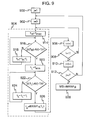
- FIG. 7 is a block diagram of a monitoring unit of the generator of FIG. 1 , the unit incorporating the signal analysis device;
- FIG. 9 is a flowchart of the operation of a time-shift comparator of the unit of FIG. 7 ;
- FIG. 10 depicts the shapes of a crosslation sum function S L ( ⁇ ) and a crosslation difference function D L ( ⁇ );
- FIG. 11 is a block diagram of a modified version of the signal analysis device of FIG. 7 ;
- FIG. 12 shows a different modified version of the signal analysis device
- this shows a random number generator which uses a signal analysis device in accordance with the present invention.
- the random number generator comprises a physical random signal source (PRS) which generates a chaotic output signal x(t).
- PRS physical random signal source
- a typical waveform of the signal x(t) is shown in each of FIGS. 2 a ) and 2 b ).
- the signal x(t) is delivered to an analog-to-digital converter (ADC), which also receives sampling pulses from a sampling pulse generator (SPG).
- ADC analog-to-digital converter
- SPG sampling pulse generator
- the chaotic signal x(t) is sampled by a sampler (SMP) at intervals corresponding to the period between sampling pulses, and each analog output is applied to an amplitude quantiser (QUA).
- the quantiser generates J different quantisation levels, against which the analog input sample is compared.
- OP output a digital number is produced in dependence upon the level of the analog sample.
- the random number generator generates, at intervals corresponding to the period between sampling pulses, random numbers distributed within the range 0 to J.
- a monitoring device receives the chaotic signal x(t) and the quantisation levels 1 to J from the quantiser (QUA) and generates a monitor output (MOP) which indicates whether or not the random numbers can be expected to be statistically independent, as will be explained in further detail below.
- the monitoring device is shown in FIG. 7 , and comprises a signal analysis device (also referred to herein as a crosslator) (CRS) in accordance with the present invention.
- CRS signal analysis device
- PTS parallel to serial converter
- the crosslator (CRS) outputs a crosslation function (as explained below) at an output (CFO) to a time shift comparator (TSC).
- TSC time shift comparator
- the time shift comparator (TSC) derives a signal MSI, which represents the minimum sampling interval required to obtain statistically independent samples.
- a comparator (CMP) compares this value with a value SPI representing the current sampling pulse interval.
- the comparator generates the monitor output (MOP), which indicates whether or not the current sampling pulse interval exceeds the calculated minimum sampling interval, as it should for correct operation.
- MOP monitor output
- this shows the signal x(t), which represents a random, chaotic or other irregular process continuous in time, and a constant level (threshold) of value L.
- a constant level threshold
- the resulting time instants t + 1 , t + 2 , . . . , t + k ⁇ 1 , t + k , t + k+1, . . . form a set of upcrossings of level L; those upcrossings are marked with dots in FIG. 2 a ).
- each upcrossing of level L defines a corresponding time-shifted copy of the underlying signal x(t).
- FIG. 3 The trajectories of FIG. 3 are also shown superimposed in FIG. 4 as functions of the relative time ⁇ .
- FIG. 5 depicts an empirical forward crosslation function C + L ( ⁇ ) obtained by averaging the trajectories shown in FIG. 4 .
- the time instants are determined at which the signal x(t) crosses the level L with a negative slope.
- the threshold level L is always positive.
- bipolar signals several approaches are possible:
- the forward crosslation (FC) function and the backward crosslation (BC) function provide a useful characterization of the process under investigation. For example, for positive values of the relative time ⁇ , the forward crosslation (FC) function facilitates the prediction of future values of a process given that the process has crossed at some time instant a predetermined level with a positive slope. For negative values of ⁇ , the forward crosslation (FC) function describes the average behaviour of the process prior to the upcrossing time instant.
- the backward crosslation (BC) function facilitates the prediction of future values of a process given that the process has crossed a predetermined level with a negative slope.
- the backward crosslation (BC) function describes the average behaviour of the process prior to the downcrossing time instant.
- the forward crosslation (FC) function and/or the backward crosslation (BC) function can be derived using the crosslator (CRS) shown in FIG. 7 .
- CRS crosslator
- the crosslator (CRS) forming part of the monitor (MON) of FIG. 7 and the modified crosslators to be described below, may be formed as general-purpose devices, possibly constructed on a separate integrated circuit, for use in a variety of different applications. Some of the functionality provided by the crosslators may not be required in certain applications, and indeed not all the functions to be described below are necessary for use in the monitor (MON) of FIG. 7 .
- the crosslator comprises a polarity-reversal circuit (PRC), an analogue delay line (TDL) with multiple taps, a level crossing detector (LCD), two pulse delay circuits (PDL and DEL), a pulse counter (PCT), a plurality of sample-and-hold circuits (SHC), a plurality of accumulators (ACC) and a storage register (SRG).
- PRC polarity-reversal circuit
- TDL an analogue delay line
- LCD level crossing detector
- PDL and DEL two pulse delay circuits
- PCT pulse counter
- SHC sample-and-hold circuits
- ACC accumulators
- SRG storage register
- the storage register (SRG) may also incorporate a suitable waveform interpolator.
- the polarity (positive or negative) of a time-varying input signal x(t) is set by an appropriate value held at a binary polarity-select input (PS) of the polarity-reverse circuit (PRC).
- PS binary polarity-select input
- PRC polarity-reverse circuit
- IP input
- each of M taps of the delay line (TDL) provides a time-delayed replica of the signal appearing at the input (IP).
- the signal samples observed at the M taps of the delay line (TDL) form jointly a discrete-time representation of a finite segment of the signal propagating along the delay line (TDL).
- the relative delay between consecutive taps of the delay line (TDL) has a constant value.
- Each of the M taps of the delay line (TDL) is connected to a respective sample-and-hold circuit (SHC), and a selected tap (CT), preferably the center tap, is also connected to the level crossing detector (LCD).
- SHC sample-and-hold circuit
- CT selected tap
- LCD level crossing detector
- the level crossing detector detects either upcrossings or downcrossings, depending on the value held at a binary selector input (UD).
- the desired crossing level L is set by applying a suitable threshold value to a threshold input (LV) of the level crossing detector (LCD).
- LV threshold input
- the level crossing detector When the forward crosslation (FC) function is to be determined, the level crossing detector (LCD) operates as a detector of upcrossings.
- the backward crosslation (BC) function is to be determined, the level crossing detector (LCD) detects downcrossings.
- a short trigger pulse is generated at the level crossing detector (LCD) output.
- the trigger pulse (TP) initiates, via a common trigger pulse (TP) input, the simultaneous operation of all sample-and-hold circuits (SHC).
- SHC sample-and-hold circuits captures the instantaneous value of the signal appearing at its input and supplies this value to a respective accumulator (ACC).
- the trigger pulse (TP) also increments by one the current state of the pulse counter (PCT).
- the capacity of the pulse counter (PCT) is equal to a predetermined number N of level crossings (i.e. the number N of signal trajectories being processed).
- the trigger pulse (TP) is also applied to a suitable pulse delay circuit (PDL) whose delay is preferably equal to the settling time of the sample-and-hold circuits (SHC).
- PDL pulse delay circuit
- a delayed trigger pulse obtained from the pulse delay circuit PDL initiates, via a common accumulator input (DT), the simultaneous operation of all accumulators (ACC) driven by respective sample-and-hold circuits (SHC).
- the function of each accumulator (ACC) is to perform addition or averaging of all N samples appearing successively at its input during one full operation cycle of the crosslator (CRS).
- an end-of-cycle (EC) pulse is produced at the output of the pulse counter (PCT).
- the end-of-cycle (EC) pulse resets the pulse counter (PCT), via a reset input (RT) thereof, and it also initiates the transfer of the accumulators' contents to the storage register (SRG).
- Each end-of-cycle (EC) pulse suitably delayed by the pulse delay circuit (DEL), sets all the accumulators (ACC) to their initial zero state via a common input reset (RS).
- RS common input reset
- the determined forward crosslation (FC) function is represented by M values.
- some additional signal processing may be performed in the storage register (SRG) to produce an interpolated (smoothed) representation of the forward crosslation (FC) function comprising more than M primary values supplied by the accumulators (ACC).
- the signal x(t) processed by the crosslator was generated by a physical noise source.
- the delay introduced by the level crossing detector (LCD) may be excessive and should be compensated.
- the delay compensation can for example be accomplished by employing one of the following two approaches:
- the level crossing detector (LCD) is driven by a tap preceding center the tap (CT), and such obtained pre-trigger pulse is additionally delayed at the level crossing detector (LCD) output by an auxiliary circuit, so that the total delay introduced (by the level crossing detector (LCD) and the circuit) matches the relative delay between the two taps.
- a dedicated pre-trigger tap is provided by the delay time (TDL), the pre-trigger tap preceding the center tap (CT), and the relative delay between the two taps matching that of the level crossing detector (LCD).
- the crosslator is also operable to handle bipolar signals and to derive respective functions based on both positive and negative threshold crossings.
- the polarity-reverse circuit PRC is caused by the signal at polarity-select input (PS) to reverse the polarity of the input signal x(t) so that the level crossing detector (LCD) can use a corresponding positive crossing level for deriving the required function.
- the parallel to serial converter PTS
- PLS parallel to serial converter
- LV threshold input
- UD level crossing detector
- the crosslation function has a significant value if the modulus of the difference between its value and the average value AV of the input function x(t) is greater than a threshold TH. Accordingly, the value is significant within the range ⁇ a to + ⁇ b .
- sampling interval is less than
- the sampling level is less than
- the time-shift comparator examines the crosslation function to determine the maximum value of
- the input (UD) is then switched so that the crosslator produces the backward crosslation function at its output, and the time-shift comparator again operates to find the maximum value
- the parallel to serial converter (PTS) is operated to transfer the second quantisation level to the level crossing detector (LCD) and the crosslator operations are repeated so as to obtain the forward and backward crosslation functions. This sequence is carried out for each of the quantisation levels 1 to J.
- the minimum sample interval MSI is then calculated as:
- the procedure shown in a block 904 is intended to derive the value ⁇ ij .
- i is incremented (to select backward crosslation), and at step 908 i is checked to see whether it has yet exceeded 1. If not, the procedure 904 is repeated in order to derive the value ⁇ ij for backward crosslation.
- step 908 detects that i has exceeded 1, so the program proceeds to step 910 .
- the value j is incremented so as to select the next quantisation level.
- the program determines that the final quantisation value J has not yet been exceeded, and therefore the steps 902 to 910 are repeated.
- the values ⁇ ij are calculated during procedure 904 for all values for j and for both forward and backward crosslation functions.
- the procedure 904 involves initially setting a variable ⁇ H equal to the maximum possible value of ⁇ , ⁇ max at step 914 .
- the program determines the difference between the value of the crosslation function at this point ⁇ H , i.e. V( ⁇ H ), minus the mean value AV of the input signal x(t). The program then determines whether the modulus of this difference is greater than the predetermined threshold TH. Because the program starts by looking at the highest value of ⁇ , ⁇ max , the crosslation function will be approximately equal to the mean level AV, so the program would then proceed to step 918 . At this point, the value of ⁇ H is decreased by an incremental quantity ⁇ i (representing the delay between successive stages of the delay line (DTL)). Step 916 is repeated.
- the program examines the crosslation functions, starting at the highest value ⁇ max , until step 916 detects that the crosslation functions steps outside the threshold TH. At this point, the program proceeds to step 920 .
- the program sets another variable ⁇ L , equal to the minimum possible value of ⁇ , ⁇ min .
- the program then proceeds to step 922 .
- the program determines whether the difference between the correlation function for the current value ⁇ L and the average value AV exceeds the threshold TH. If not, the program proceeds to step 924 where ⁇ L is increased by the incremental value ⁇ i .
- the program then returns to step 922 . This continues, with the program successively checking the crosslation function for increasing values of ⁇ until the value falls outside the threshold region. The program then proceeds to step 926 .
- the program sets the value ⁇ ij equal to the maximum of ⁇ H and ⁇ L and stores the value ⁇ ij for later use.
- step 912 the program proceeds from step 912 to step 928 , where the minimum sampling interval MIS is set equal to the maximum value of all the stored ⁇ ij values.
- This value is sent to the comparator (CMP) which compares the value with the value SPI representing the actual sampling interval. If the actual sampling interval is greater than MSI, then the comparator output (MSP) indicates that successive random numbers are expected to be statistically independent. If desired, the comparator output can be used to control the sampling interval, i.e. to increase it if the current sampling interval is determined to be smaller than MSI.
- FC forward crosslation
- BC backward crosslation
- the crosslation sum (CS) function S L ( ⁇ ) provides information somewhat similar to that provided by the conventional autocorrelation function.
- the crosslation sum function of a Gaussian process is proportional to the autocorrelation function of that process.
- the crosslation sum (CS) function of any time-reversible process is an even function of its argument, the relative delay ⁇ .
- the crosslation difference (CD) function D L ( ⁇ ) provides information related to that provided by the derivative of the conventional autocorrelation function.
- the crosslation difference (CD) function of a Gaussian process is proportional to the negated derivative of the autocorrelation function of that process.
- the crosslation difference (CD) function of any time-reversible process is an odd function of its argument, the relative delay ⁇ .
- the crosslation sum (CS) function and the crosslation difference (CD) function can be determined for a continuous-time signal x(t) with the use of a modified crosslator (CRS) shown in FIG. 11 .
- the system comprises a polarity-reversal circuit (PRC), an analogue delay line with multiple taps (TDL), a level crossing processor (LCP), two pulse delay circuits (PDL and DEL), a pulse counter (PCT), a plurality of sample-and-hold circuits (SHC), a plurality of add/subtract accumulators (ASA) and a storage register (SRG).
- the storage register (SRG) may also incorporate a suitable waveform interpolator.
- the operations performed by the modified crosslator differ from those performed by the basic crosslator (CRS) in FIG. 7 as follows.
- the level crossing processor (LCP) produces a short trigger pulse (TP) each time a level crossing (upcrossing or downcrossing) is detected at the center tap (CT) of the delay line (TDL).
- the desired crossing level L is set by applying a suitable threshold value to the threshold input (LV) of the level crossing processor (LCP).
- the required operation mode, to determine the crosslation sum function or the crosslation difference function, is selected by applying a suitable value to a binary selector input (SD) of the level crossing processor (LCP).
- Each add/subtract accumulator adds or subtracts sample values supplied by a respective sample-and-hold circuit (SHC), depending on the command, ‘ADD’ or ‘SUBTRACT’, appearing at its control input (AS).
- SHC sample-and-hold circuit
- the level crossing processor LCP sends command ‘ADD’, via the common control input (AS), to all the add/subtract accumulators (ASA), irrespective of the type of a detected level crossing (upcrossing or downcrossing).
- the level crossing processor LCP sends command ‘ADD’ for each detected upcrossing, and command ‘SUBTRACT’ for each detected downcrossing. Because in a continuous-time signal upcrossings and downcrossings (of the same level) alternate, the operations ADD and SUBTRACT will also alternate following the crossings pattern.
- the crosslator (CRS) of FIG. 11 could be used in the monitor (MON) of FIG. 7 by, for example, generating only a crosslation sum for each quantization level, and using the time-shift comparator (TSC) to calculate the maximum delay value
- TSC time-shift comparator
- FIG. 12 is a block diagram of the basic crosslator of FIG. 7 incorporating a SIPO shift register (SIPOSR).
- the system also comprises a signal conditioning unit (SCU), a clock generator (CKG), a level crossing detector (LCD), two pulse delay circuits (PDL and DEL), a pulse counter (PCT), a plurality of sample-and-hold circuits (SHC), a plurality of accumulators (ACC) and a storage register (SRG).
- the storage register (SRG) may also incorporate a suitable waveform interpolator.
- An analogue continuous-time signal x(t) is converted by a signal conditioning unit (SCU) into a suitable (analogue or digital) form and then applied to the serial input (IP) of the SIPOSR.
- SCU signal conditioning unit
- IP serial input
- the SIPO shift register consists of M storage cells, C 1 , C 2 , . . . , CM. Each cell has an input terminal, an output terminal and a clock terminal (CP).
- the cells are connected serially so that each cell, except for the first one (C 1 ) and the last one (CM), has its input terminal connected to the output terminal of a preceding cell and its output terminal connected to the input terminal of a succeeding cell.
- the input terminal of cell C 1 is used as the serial input (CP) of the SIPO shift register.
- the output terminals of all M cells are regarded as the parallel output terminals of the SIPO shift register. All clock terminals (CP) of the cells are connected together to form the clock terminal of the SIPO shift register.
- a sequence of suitable clock pulses is provided by a clock generator (CKG).
- CKG clock generator
- the signal sample stored in each cell is transferred (shifted) to and stored by the succeeding cell; cell C 1 stores the value x(to) of the input signal x(t).
- the shift register can be implemented either as a digital device or as a discrete-time analogue device, for example, in the form of a “bucket-brigade” charge-coupled device (CCD).
- the parallel outputs of the SIPO shift register are connected to respective M sample-and-hold circuits (SHC).
- SHC sample-and-hold circuits
- Two selected adjacent SIPOSR outputs are also connected to two inputs of the level crossing detector (LCD).
- the selected outputs are those of cell CY and cell CZ.
- the two selected outputs are preferably output M/2 and output M/2+1.
- the SPO shift register is operating in discrete time, defined by clock pulses provided by the clock generator (CKG), the detection of crossing a predetermined level L by signal samples is slightly more complicated. However, the crossing detection can be accomplished by applying the following decision rule:
- the ‘time’ location of the virtual cell VC is uniformly distributed over the clock period. Consequently, the virtual cell VC is ‘located’ in the middle between cell CY and cell CZ.
- the crosslators (CRS) described above enable the generation of separate forward and backward crosslation functions (from which crosslation sum and crosslation difference functions can be derived), or the direct generation of crosslation sum and crosslation difference functions. Those functions can be generated for respective different crossing levels, which may be both positive and negative.
- the input signal x(t) has an average value AV of zero which enables simplification of the processing of the crosslation functions.
- crosslation function or combination of functions
- crosslation sum and/or crosslation difference functions the functions can be derived for a single crossing level or for multiple crossing levels.
- non-Gaussian signals it is more informative to use one or more crossing levels which are significantly different from the mean AV of the signal x(t).
- each function corresponds to a respective crossing level. It would be possible to derive additional functions which relate to a combination of (for example the difference between) crosslation functions relating to respective different crossing levels.
- the crosslation function i.e. either forward or backward crosslation function
- the resulting function is a scaled replica of the autocorrelation function.
- the crosslator could be arranged to distinguish between slopes of different magnitude in each of the positive and negative directions; that is, the slope could be represented by two or more bits, rather than a single bit (representative of either positive or negative slope).
- the arrangement may be such that only certain quantised slope levels (e.g. the steepest slopes) are taken into consideration in deriving a crosslation function.
- the input signal x(t) could represent any physical quantity of interest, such as noise, pressure, displacement, velocity, temperature, etc. Accordingly, the invention has wide fields of application, such as communications, radio astronomy, remote sensing, underwater acoustics, geophysics, speech analysis, biomedicine, etc. Although the specific examples given above refer to an input signal which varies with time, the argument of the function may represent any appropriate independent variable, such as relative time, distance, spatial location, angular position, etc.
- the crosslator is formed of a separate integrated circuit device, it is preferably provided with an input terminal for the input signal x(t), a threshold terminal for receiving a signal (LV) representing the crossing level and at least one output terminal for providing the output function (CSO) in either parallel or serial form.
- a derived crosslation function may be used for classification purposes, whereby the derived crosslation waveform, for example the crosslation sum waveform, is used to indicate a specific class which best represents the object generating the signal.
- a suitable memory may be provided to store a set of representative templates' of crosslation waveforms (each template corresponding to a respective class and representing the shape of a crosslation function for that class). The classification may be carried out by finding the best match between a suitable representation of the determined crosslation function and the stored templates.
- the shape of the crosslation waveform may be regarded as a ‘fingerprint’ signature used to discriminate between several (including ‘unknown’) classes of signal emitting objects.
Abstract
Description
t + 1 , t + 2 , . . . , t + k−1 , t + k , t + k+1, . . .
form a set of upcrossings of level L; those upcrossings are marked with dots in
x + k(τ)=x(t + k+τ)
where τ is the relative time. Therefore, the selected trajectory x+ k(τ), shown in
t − 1 , t − 2 , . . . , t − m−1 , t − m , t − m+1, . . .
shown in
S L(τ)=C + L(τ)+C − L(τ)
is referred to as the crosslation sum (CS) function, and a typical example is shown in
D L(τ)=C + L(τ)−C − L(τ)
is referred to as the crosslation difference (CD) function. A typical example is also shown in
Claims (23)
Applications Claiming Priority (2)
| Application Number | Priority Date | Filing Date | Title |
|---|---|---|---|
| EP02254612A EP1378854B1 (en) | 2002-07-01 | 2002-07-01 | Signal statistics determination |
| EP02254612.1 | 2002-07-01 |
Publications (2)
| Publication Number | Publication Date |
|---|---|
| US20040059517A1 US20040059517A1 (en) | 2004-03-25 |
| US7120555B2 true US7120555B2 (en) | 2006-10-10 |
Family
ID=29719768
Family Applications (1)
| Application Number | Title | Priority Date | Filing Date |
|---|---|---|---|
| US10/609,375 Expired - Lifetime US7120555B2 (en) | 2002-07-01 | 2003-07-01 | Signal statistics determination |
Country Status (5)
| Country | Link |
|---|---|
| US (1) | US7120555B2 (en) |
| EP (1) | EP1378854B1 (en) |
| JP (1) | JP4612286B2 (en) |
| CN (1) | CN1330943C (en) |
| DE (1) | DE60224263T2 (en) |
Cited By (3)
| Publication number | Priority date | Publication date | Assignee | Title |
|---|---|---|---|---|
| EP2226639A1 (en) | 2009-03-03 | 2010-09-08 | Mitsubishi Electric R&D Centre Europe B.V. | Spectral analysis and FMCW automotive radar utilizing the same |
| EP2226640A1 (en) | 2009-03-03 | 2010-09-08 | Mitsubishi Electric R&D Centre Europe B.V. | Spectral analysis |
| EP2287748A1 (en) | 2009-08-21 | 2011-02-23 | Mitsubishi Electric R&D Centre Europe B.V. | Determination of system characteristics |
Families Citing this family (8)
| Publication number | Priority date | Publication date | Assignee | Title |
|---|---|---|---|---|
| EP1306805A1 (en) * | 2001-10-25 | 2003-05-02 | Mitsubishi Electric Information Technology Centre Europe B.V. | Image Analysis |
| EP1528407A1 (en) | 2003-10-31 | 2005-05-04 | Mitsubishi Electric Information Technology Centre Europe B.V. | Decomposition of a wideband random signal |
| EP1596219A1 (en) | 2004-05-13 | 2005-11-16 | Mitsubishi Electric Information Technology Centre Europe B.V. | Signal processing circuit for time delay determination |
| US7453765B2 (en) * | 2006-05-16 | 2008-11-18 | Ikelle Luc T | Scattering diagrams in seismic imaging |
| JP2008182425A (en) * | 2007-01-24 | 2008-08-07 | Denso Corp | Filter circuit |
| EP2221732A1 (en) | 2009-02-23 | 2010-08-25 | Mitsubishi Electric R&D Centre Europe B.V. | Signal processing |
| WO2011162166A1 (en) * | 2010-06-25 | 2011-12-29 | Semiconductor Energy Laboratory Co., Ltd. | Liquid crystal display device and electronic appliance |
| CN112422360A (en) * | 2020-10-14 | 2021-02-26 | 锐捷网络股份有限公司 | Message sampling method, device, equipment and medium |
Citations (15)
| Publication number | Priority date | Publication date | Assignee | Title |
|---|---|---|---|---|
| US3732405A (en) | 1971-08-11 | 1973-05-08 | Nasa | Apparatus for statistical time-series analysis of electrical signals |
| US3737788A (en) * | 1965-06-11 | 1973-06-05 | North American Rockwell | Slope responsive signal identification means |
| US3896395A (en) * | 1974-07-18 | 1975-07-22 | Bell Telephone Labor Inc | Linear amplification using quantized envelope components to phase reverse modulate quadrature reference signals |
| US4122393A (en) * | 1977-05-11 | 1978-10-24 | Ncr Corporation | Spread spectrum detector |
| US4387465A (en) * | 1981-04-13 | 1983-06-07 | Trw Inc. | Sequential threshold detector |
| US4638185A (en) * | 1983-11-15 | 1987-01-20 | Iwatsu Electric Co., Ltd. | Analog signal measuring apparatus |
| US4843309A (en) * | 1988-03-21 | 1989-06-27 | Tektronix, Inc. | Waveform timing alignment system for digital oscilloscopes |
| US4897855A (en) * | 1987-12-01 | 1990-01-30 | General Electric Company | DPCM system with adaptive quantizer having unchanging bin number ensemble |
| US5272725A (en) * | 1991-02-25 | 1993-12-21 | Alliedsignal Inc. | Digital video quantizer |
| US6205168B1 (en) * | 1998-11-12 | 2001-03-20 | Sharp Laboratories Of America, Inc. | Sequential detection system and method with adaptive bias |
| US6249556B1 (en) * | 1998-05-27 | 2001-06-19 | Intel Corporation | Dynamic thresholding for input receivers |
| US20030035549A1 (en) * | 1999-11-29 | 2003-02-20 | Bizjak Karl M. | Signal processing system and method |
| US6539320B1 (en) | 1998-12-24 | 2003-03-25 | Mitsubishi Denki Kabushiki Kaisha | Time delay determination and determination of signal shift |
| US20040185353A1 (en) * | 2003-03-17 | 2004-09-23 | Seiko Epson Corporation | Aligner, exposing method, method for manufacturing thin-film transistor, display device, and electronic device using shading means |
| US20040183531A1 (en) * | 2001-07-10 | 2004-09-23 | Robinson John W.C. | Method of estimating target signals by a dynamical fluxgate sensor |
Family Cites Families (5)
| Publication number | Priority date | Publication date | Assignee | Title |
|---|---|---|---|---|
| JP2980576B2 (en) * | 1997-09-12 | 1999-11-22 | 株式会社東芝 | Physical random number generating apparatus and method, and physical random number recording medium |
| JP2000066592A (en) * | 1998-08-19 | 2000-03-03 | Syst Kogaku Kk | Random number generating apparatus |
| JP2000089672A (en) * | 1998-09-09 | 2000-03-31 | Ntt Data Corp | Enciphering circuit and random password generation circuit |
| JP3447976B2 (en) * | 1999-03-26 | 2003-09-16 | システム工学株式会社 | Random number generator with failure judgment function |
| US6571186B1 (en) * | 1999-09-14 | 2003-05-27 | Textronix, Inc. | Method of waveform time stamping for minimizing digitization artifacts in time interval distribution measurements |
-
2002
- 2002-07-01 EP EP02254612A patent/EP1378854B1/en not_active Expired - Lifetime
- 2002-07-01 DE DE60224263T patent/DE60224263T2/en not_active Expired - Lifetime
-
2003
- 2003-07-01 JP JP2003189764A patent/JP4612286B2/en not_active Expired - Fee Related
- 2003-07-01 CN CNB031545033A patent/CN1330943C/en not_active Expired - Fee Related
- 2003-07-01 US US10/609,375 patent/US7120555B2/en not_active Expired - Lifetime
Patent Citations (15)
| Publication number | Priority date | Publication date | Assignee | Title |
|---|---|---|---|---|
| US3737788A (en) * | 1965-06-11 | 1973-06-05 | North American Rockwell | Slope responsive signal identification means |
| US3732405A (en) | 1971-08-11 | 1973-05-08 | Nasa | Apparatus for statistical time-series analysis of electrical signals |
| US3896395A (en) * | 1974-07-18 | 1975-07-22 | Bell Telephone Labor Inc | Linear amplification using quantized envelope components to phase reverse modulate quadrature reference signals |
| US4122393A (en) * | 1977-05-11 | 1978-10-24 | Ncr Corporation | Spread spectrum detector |
| US4387465A (en) * | 1981-04-13 | 1983-06-07 | Trw Inc. | Sequential threshold detector |
| US4638185A (en) * | 1983-11-15 | 1987-01-20 | Iwatsu Electric Co., Ltd. | Analog signal measuring apparatus |
| US4897855A (en) * | 1987-12-01 | 1990-01-30 | General Electric Company | DPCM system with adaptive quantizer having unchanging bin number ensemble |
| US4843309A (en) * | 1988-03-21 | 1989-06-27 | Tektronix, Inc. | Waveform timing alignment system for digital oscilloscopes |
| US5272725A (en) * | 1991-02-25 | 1993-12-21 | Alliedsignal Inc. | Digital video quantizer |
| US6249556B1 (en) * | 1998-05-27 | 2001-06-19 | Intel Corporation | Dynamic thresholding for input receivers |
| US6205168B1 (en) * | 1998-11-12 | 2001-03-20 | Sharp Laboratories Of America, Inc. | Sequential detection system and method with adaptive bias |
| US6539320B1 (en) | 1998-12-24 | 2003-03-25 | Mitsubishi Denki Kabushiki Kaisha | Time delay determination and determination of signal shift |
| US20030035549A1 (en) * | 1999-11-29 | 2003-02-20 | Bizjak Karl M. | Signal processing system and method |
| US20040183531A1 (en) * | 2001-07-10 | 2004-09-23 | Robinson John W.C. | Method of estimating target signals by a dynamical fluxgate sensor |
| US20040185353A1 (en) * | 2003-03-17 | 2004-09-23 | Seiko Epson Corporation | Aligner, exposing method, method for manufacturing thin-film transistor, display device, and electronic device using shading means |
Non-Patent Citations (1)
| Title |
|---|
| IBM Technical Disclosure Bulletin, vol. 20, No. 11A, Apr. 1978, pp. 4280-4282. |
Cited By (6)
| Publication number | Priority date | Publication date | Assignee | Title |
|---|---|---|---|---|
| EP2226639A1 (en) | 2009-03-03 | 2010-09-08 | Mitsubishi Electric R&D Centre Europe B.V. | Spectral analysis and FMCW automotive radar utilizing the same |
| EP2226640A1 (en) | 2009-03-03 | 2010-09-08 | Mitsubishi Electric R&D Centre Europe B.V. | Spectral analysis |
| US20100225524A1 (en) * | 2009-03-03 | 2010-09-09 | Wieslaw Jerzy Szajnowski | Spectral analysis and fmcw automotive radar utilizing the same |
| US8223064B2 (en) | 2009-03-03 | 2012-07-17 | Mitsubishi Electric Corporation | Spectral analysis and FMCW automotive radar utilizing the same |
| EP2287748A1 (en) | 2009-08-21 | 2011-02-23 | Mitsubishi Electric R&D Centre Europe B.V. | Determination of system characteristics |
| WO2011020738A1 (en) | 2009-08-21 | 2011-02-24 | Mitsubishi Electric R&D Centre Europe B.V. | Determination of system characteristics |
Also Published As
| Publication number | Publication date |
|---|---|
| EP1378854A1 (en) | 2004-01-07 |
| US20040059517A1 (en) | 2004-03-25 |
| DE60224263D1 (en) | 2008-02-07 |
| CN1330943C (en) | 2007-08-08 |
| JP4612286B2 (en) | 2011-01-12 |
| JP2004163889A (en) | 2004-06-10 |
| CN1495414A (en) | 2004-05-12 |
| EP1378854B1 (en) | 2007-12-26 |
| DE60224263T2 (en) | 2008-12-11 |
Similar Documents
| Publication | Publication Date | Title |
|---|---|---|
| US7120555B2 (en) | Signal statistics determination | |
| US20160231357A1 (en) | Method and apparatus for data acquisition with waveform trigger | |
| JP5864857B2 (en) | Time delay estimation | |
| EP0335496B1 (en) | Waveform timing alignment system for digital oscilloscopes | |
| US8604953B2 (en) | Calibrating timing, gain and bandwidth mismatch in interleaved ADCs | |
| US20120041701A1 (en) | Time-domain triggering in a test and measurement instrument | |
| EP0585237A1 (en) | Dynamical system analyser | |
| JP2005354676A (en) | Signal processing circuit and method or time delay detection apparatus and object position specification apparatus using the method | |
| US5774085A (en) | Apparatus and method for obtaining proper output signal in which gain and DC component are regulated based upon on measured amplitude distribution | |
| JP2014077791A (en) | Method of indicating correlation between multiple signals, and test measurement device | |
| US10733468B2 (en) | Finger stability detecting method and fingerprint sensing device | |
| US4516220A (en) | Pulse deinterleaving signal processor and method | |
| JP6148229B2 (en) | Dynamic clustering of transition signals | |
| JP5605834B2 (en) | Test and measurement equipment | |
| US10670703B2 (en) | Device for detecting a laser spot | |
| JPH04132328A (en) | Spread spectrum communication equipment | |
| JP3846330B2 (en) | Collected data synchronization method and data processing system | |
| US4254470A (en) | Interpolating digital data processing apparatus for correlation-type flow measurement | |
| Delagnes | What is the theoretical time precision achievable using a dCFD algorithm? | |
| JP3082571B2 (en) | Signal processing device | |
| JP2021520094A (en) | Floating input detection | |
| RU2700798C2 (en) | Apparatus for detecting broadband polyharmonic signals on background of additive interference | |
| RU2342781C2 (en) | Device for amplitude and frequency distortions compensation in line link using 2d metric domain | |
| SU809017A1 (en) | Device for signal non-parametric processing | |
| Wüstner et al. | Sophisticated online analysis in ADC boards |
Legal Events
| Date | Code | Title | Description |
|---|---|---|---|
| AS | Assignment |
Owner name: MITSUBISHI ELECTRONIC INFORMATION TECHNOLOGY CENTR Free format text: ASSIGNMENT OF ASSIGNORS INTEREST;ASSIGNOR:SZAJNOWSKI, WIESLAW JERZY;REEL/FRAME:014593/0924 Effective date: 20030812 |
|
| AS | Assignment |
Owner name: MITSUBISHI DENKI KABUSHIKI KAISHA, JAPAN Free format text: ASSIGNMENT OF ASSIGNORS INTEREST;ASSIGNOR:MITSUBISHI ELECTRIC INFORMATION TECHNOLOGY CENTRE EUROPE B.V.;REEL/FRAME:016459/0394 Effective date: 20031106 |
|
| STCF | Information on status: patent grant |
Free format text: PATENTED CASE |
|
| FEPP | Fee payment procedure |
Free format text: PAYOR NUMBER ASSIGNED (ORIGINAL EVENT CODE: ASPN); ENTITY STATUS OF PATENT OWNER: LARGE ENTITY |
|
| FPAY | Fee payment |
Year of fee payment: 4 |
|
| FPAY | Fee payment |
Year of fee payment: 8 |
|
| MAFP | Maintenance fee payment |
Free format text: PAYMENT OF MAINTENANCE FEE, 12TH YEAR, LARGE ENTITY (ORIGINAL EVENT CODE: M1553) Year of fee payment: 12 |