US7121742B2 - Optical module - Google Patents
Optical module Download PDFInfo
- Publication number
- US7121742B2 US7121742B2 US10/655,589 US65558903A US7121742B2 US 7121742 B2 US7121742 B2 US 7121742B2 US 65558903 A US65558903 A US 65558903A US 7121742 B2 US7121742 B2 US 7121742B2
- Authority
- US
- United States
- Prior art keywords
- block
- assembly
- optical
- substrate
- receptacle
- Prior art date
- Legal status (The legal status is an assumption and is not a legal conclusion. Google has not performed a legal analysis and makes no representation as to the accuracy of the status listed.)
- Expired - Lifetime, expires
Links
Images


Classifications
-
- G—PHYSICS
- G02—OPTICS
- G02B—OPTICAL ELEMENTS, SYSTEMS OR APPARATUS
- G02B6/00—Light guides; Structural details of arrangements comprising light guides and other optical elements, e.g. couplings
- G02B6/24—Coupling light guides
- G02B6/42—Coupling light guides with opto-electronic elements
- G02B6/4292—Coupling light guides with opto-electronic elements the light guide being disconnectable from the opto-electronic element, e.g. mutually self aligning arrangements
-
- G—PHYSICS
- G02—OPTICS
- G02B—OPTICAL ELEMENTS, SYSTEMS OR APPARATUS
- G02B6/00—Light guides; Structural details of arrangements comprising light guides and other optical elements, e.g. couplings
- G02B6/24—Coupling light guides
- G02B6/42—Coupling light guides with opto-electronic elements
- G02B6/4201—Packages, e.g. shape, construction, internal or external details
- G02B6/4256—Details of housings
- G02B6/4257—Details of housings having a supporting carrier or a mounting substrate or a mounting plate
-
- G—PHYSICS
- G02—OPTICS
- G02B—OPTICAL ELEMENTS, SYSTEMS OR APPARATUS
- G02B6/00—Light guides; Structural details of arrangements comprising light guides and other optical elements, e.g. couplings
- G02B6/24—Coupling light guides
- G02B6/42—Coupling light guides with opto-electronic elements
- G02B6/4201—Packages, e.g. shape, construction, internal or external details
- G02B6/4274—Electrical aspects
- G02B6/4284—Electrical aspects of optical modules with disconnectable electrical connectors
-
- G—PHYSICS
- G02—OPTICS
- G02B—OPTICAL ELEMENTS, SYSTEMS OR APPARATUS
- G02B6/00—Light guides; Structural details of arrangements comprising light guides and other optical elements, e.g. couplings
- G02B6/24—Coupling light guides
- G02B6/42—Coupling light guides with opto-electronic elements
- G02B6/4201—Packages, e.g. shape, construction, internal or external details
- G02B6/4246—Bidirectionally operating package structures
-
- G—PHYSICS
- G02—OPTICS
- G02B—OPTICAL ELEMENTS, SYSTEMS OR APPARATUS
- G02B6/00—Light guides; Structural details of arrangements comprising light guides and other optical elements, e.g. couplings
- G02B6/24—Coupling light guides
- G02B6/42—Coupling light guides with opto-electronic elements
- G02B6/4201—Packages, e.g. shape, construction, internal or external details
- G02B6/4256—Details of housings
- G02B6/4262—Details of housings characterised by the shape of the housing
- G02B6/4263—Details of housings characterised by the shape of the housing of the transisitor outline [TO] can type
-
- G—PHYSICS
- G02—OPTICS
- G02B—OPTICAL ELEMENTS, SYSTEMS OR APPARATUS
- G02B6/00—Light guides; Structural details of arrangements comprising light guides and other optical elements, e.g. couplings
- G02B6/24—Coupling light guides
- G02B6/42—Coupling light guides with opto-electronic elements
- G02B6/4201—Packages, e.g. shape, construction, internal or external details
- G02B6/4266—Thermal aspects, temperature control or temperature monitoring
- G02B6/4268—Cooling
- G02B6/4269—Cooling with heat sinks or radiation fins
-
- G—PHYSICS
- G02—OPTICS
- G02B—OPTICAL ELEMENTS, SYSTEMS OR APPARATUS
- G02B6/00—Light guides; Structural details of arrangements comprising light guides and other optical elements, e.g. couplings
- G02B6/24—Coupling light guides
- G02B6/42—Coupling light guides with opto-electronic elements
- G02B6/4201—Packages, e.g. shape, construction, internal or external details
- G02B6/4274—Electrical aspects
- G02B6/4277—Protection against electromagnetic interference [EMI], e.g. shielding means
Definitions
- the present invention relates to an optical module including a positioning member for positioning an optical device and a circuit board formed with a circuit for driving the optical device.
- optical module constituted by a circuit board implemented with an optical sub-assembly and its driving circuit, a signal amplifying circuit, and the like, and a housing enclosing them.
- This optical module comprises a receptacle for receiving an optical connector provide data leading end of an optical fiber, whereby optical coupling is achieved between the optical sub-assembly and the optical connector within the receptacle.
- the position of the optical sub-assembly must be determined with respect to the optical connector.
- conventional optical modules For positioning the optical sub-assembly with respect to the receptacle, conventional optical modules form the receptacle with an opening for inserting the optical sub-assembly and insert the optical device into the opening, while defining the shape of the receptacle such that the relative position of the optical connector is determined with respect to the opening, whereby optical coupling is achieved between them (see, for example, U.S. Pat. No. 6,335,869).
- FIG. 10 is an exploded perspective view showing an example of a conventional optical module 60 .
- optical sub-assemblies 62 are inserted into openings 64 of a housing 61 , a circuit board 63 is enclosed in the housing 61 , and then lead pins of the optical sub-assemblies 62 and the circuit board 63 are fixed to each other.
- assembly efficiency is inferior in the method comprising the steps of separately setting the optical sub-assemblies 62 and the circuit board 63 into the housing 61 and then bonding them to each other.
- the optical module in accordance with one aspect of the present invention comprises a housing having a lower casing including a receptacle to mate with an optical connector, and a mount, an upper casing to engage the lower casing, and a cover for covering the upper casing; an optical sub-assembly optically coupling with the optical connector in the receptacle; a circuit board electrically connected to the optical sub-assembly and mounted on the mount of the lower casing; and a block, mounted on the lower casing, for defining relative positions of the lower casing, upper casing, optical sub-assembly, and circuit board.
- the block can position the circuit board and optical sub-assembly, whereby the circuit board and the optical sub-assembly can be positioned with respect to the upper and lower casings together with the block.
- the circuit board and the optical sub-assembly can be fixed to each other in the final positional relationship, thus providing an optical module with efficient assembling.
- the optical module in accordance with another aspect comprises an optical sub-assembly mounted with an optical device; a circuit board electrically connected to the optical sub-assembly; a lower casing having a receptacle for receiving an optical connector holding an optical fiber, and a mount for mounting the circuit board; an upper casing to engage the lower casing; and a resin block for defining positions of the optical sub-assembly, circuit board, lower casing, and upper casing.
- the receptacle includes an abutting surface having an opening for receiving one end of the optical sub-assembly.
- the block comprises a front wall including one surface, in contact with the abutting surface, having an opening corresponding to the opening of the receptacle and receiving one end of the optical sub-assembly; a center wall; and a pair of side walls disposing the center wall therebetween.
- the center wall has a supporting portion for holding the circuit board.
- Each of the pair of side walls has a pressing portion for pressing the circuit board. Holding the circuit board between the supporting portion and pressing portions defines relative positions of the block and circuit board.
- the mount in the lower casing provides a projection.
- the block is held between one side face of the projection and the abutting surface.
- a side wall of the block provides a first cutout.
- a side wall of the lower casing provides a second cutout.
- the upper casing is formed with first and second protrusions. The first and second cutouts engage with the first and second protrusions, respectively, thereby defining relative positions of the lower casing, upper casing, and block.
- inserting the optical sub-assembly into the opening of the front wall and holding the circuit board between the supporting portion and pressing portions can position the optical sub-assembly and circuit board with respect to the block. Therefore, before being assembled into the casings, the circuit board and the optical sub-assembly can be fixed to each other in the final positional relationship within the casings. Also, holding the block between the abutting surface of the receptacle and the projection in the lower casing can easily position the block with respect to the lower casing. Further, causing the first and second cutouts to engage with the first and second protrusions, respectively, can easily determine the relative positions of the lower casing, upper casing, and block. Hence, an optical module with easily assembled configuration.
- the optical module in accordance with still another aspect comprises an optical sub-assembly having an optical device; a circuit board electrically connected to the optical sub-assembly; a lower casing having a receptacle for receiving an optical connector holding an optical fiber, and a mount for mounting the circuit board; an upper casing to engage with the lower casing; and a resinblock for defining positions of the optical sub-assembly, circuit board, lower casing, and upper casing.
- the receptacle includes an abutting surface having an opening for receiving one end of the optical sub-assembly.
- the block comprises a front wall including one surface, in contact with the abutting surface, having an opening corresponding to the opening of the receptacle and receiving one end of the optical sub-assembly; a center wall; and a pair of side walls disposing the center wall therebetween.
- the center wall has a supporting portion for holding the circuit board.
- Each of the pair of side walls has a pressing portion for pressing the circuit board. Holding the circuit board between the supporting portion and pressing portions defines relative positions of the block and circuit board.
- An inner face of the upper casing provides a projection.
- the center wall of the block provides a cutout.
- a side wall of the block provides a first cutout.
- a side wall of the lower casing provides a second cutout.
- the upper casing provides first and second protrusions. The first and second cutouts engage with the first and second protrusions, respectively, thereby defining relative positions of the lower casing, upper casing, and block.
- inserting the optical sub-assembly into the opening of the front wall and holding the circuit board between the supporting portion and pressing portions can position the optical sub-assembly and circuit board with respect to the block. Therefore, before being assembled in the casings, the circuit board and the optical sub-assembly can be fixed to each other in the final positional relationship within the casings. Also, holding the block between the abutting surface of the receptacle in the lower casing and the projection in the upper casing can easily position the block with respect to the lower casing. Further, engaging the first and second cutouts with the first and second protrusions, respectively, can easily determine the relative positions of the lower casing, upper casing, and block. Hence, an optical module which can be easily assembled is provided.
- FIG. 1 is an exploded perspective view showing the optical module in accordance with a first embodiment
- FIG. 2 is a perspective view showing the optical module in accordance with the first embodiment
- FIGS. 3A and 3B are perspective views showing a block
- FIG. 4 is a side view showing a state where an optical sub-assembly is accommodated in a lower casing
- FIGS. 5A and 5B are views showing respective steps of making the assembly
- FIG. 6 is a perspective view showing the assembly
- FIG. 7 is a partial perspective view showing the lower casing in the first embodiment
- FIGS. 8A , 8 B, and 8 C are views showing a process of inserting the assembly into the lower casing
- FIG. 9 is a partial perspective view showing the upper casing in the first embodiment
- FIG. 10 is a perspective view showing a conventional optical module.
- FIG. 11 is a perspective view showing the upper casing in a second embodiment.
- FIG. 1 is an exploded perspective view of the optical module 1
- FIG. 2 is a perspective view of the optical module 1
- the optical module 1 comprises a transmitting optical sub-assembly 21 a and a receiving optical sub-assembly 21 b (collectively referred to as “optical sub-assembly 21 ”), a circuit board 20 on which is formed a circuit for driving the optical sub-assembly 21 , and a housing 30 for encasing the optical sub-assembly 21 and circuit board 20 .
- the optical sub-assembly 21 and the circuit board 20 are electrically connected to each other by leads extending from the optical sub-assembly 21 .
- the housing 30 comprises a lower casing 31 for receiving the optical sub-assembly 21 and circuit board 20 , an upper casing 37 , and a cover 32 for covering the lower casing 31 and upper casing 37 .
- the lower casing 31 has a mount 31 h for mounting the block 10 , including a mounting surface 31 i for mounting the circuit board 20 , and a receptacle 31 j disposed at one end of the mount 31 h.
- the receptacle 31 j has openings 31 m . Each opening 31 m receives a leading end of the optical sub-assembly 21 . An optical fiber held by an optical connector inserted into the receptacle 31 j from the other end is optically coupled to the optical sub-assembly 21 within the opening 31 m .
- the receptacle 31 j is formed with two openings 31 m for receiving the transmitting optical sub-assembly 21 a and receiving optical sub-assembly 21 b , respectively.
- the transmitting optical sub-assembly 21 a and the receiving optical sub-assembly 21 b are inserted into the openings 31 m formed in the lower casing 31 , whereas the circuit board 20 mounted on the mount 31 h of the lower casing 31 is stopped by a substrate stopper 36 , whereby the optical sub-assembly 21 and circuit board 20 are secured to the lower casing 31 .
- the circuit board 20 comprises a first substrate 20 a and a second substrate 20 b .
- the first substrate 20 a and second substrate 20 b are connected to each other by a flexible substrate 20 c .
- the flexible substrate 20 c is bent such that the first substrate 20 a and second substrate 20 b faces each other. This can realize a two-story structure as shown in FIG. 2 .
- the optical module 1 includes a block 10 for positioning the optical sub-assembly 21 and circuit board 20 , and holders 19 for securing the optical sub-assembly 21 with respect to the block 10 .
- the optical module 1 also includes brackets 33 and a shield 34 which are used for reducing noise affecting the optical sub-assembly 21 .
- the optical module 1 further includes a cap 35 attached to an end portion opposite from the receptacle 31 j of the lower casing 31 , a fin 38 , and an actuator 39 for releasing the engagement with a host board to which the optical module 1 is mounted.
- brackets 33 are attached to the outer surface of the optical sub-assembly 21 .
- the shield 34 has a substantially planar shape and has holes through which end portions of the optical sub-assembly 21 can pass.
- the shield 34 is attached to one surface of the block 10 which will be explained later.
- the fin 38 transmits the heat generated by the transmitting optical sub-assembly 21 a itself to the outside of the optical module 1 .
- One end 38 a of the fin 38 is disposed at the outer surface of the transmitting optical sub-assembly 21 a , whereas the other end 38 b is in contact with the upper face of the receptacle 31 j .
- a silicone sheet 40 is attached to one end 38 a .
- the silicone sheet 40 may contain metal fillers.
- FIGS. 3A and 3B are perspective views showing the block 10 as seen from respective directions different from each other.
- the block 10 comprises a mount 11 for mounting the optical sub-assembly 21 , a front wall 12 disposed at one end of the mount 11 , a substrate supporting portion 14 disposed at the other end of the mount 11 , and a substrate pressing portion 15 .
- the block 10 is molded from a resin.
- the mount 11 is divided into a first region 11 a for mounting the transmitting optical sub-assembly 21 a , and a second region 11 b for mounting the receiving optical sub-assembly 21 b.
- the front wall 12 is formed with openings 12 a , 12 b into which respective head portions of the transmitting optical sub-assembly 21 a and receiving optical sub-assembly 21 b placed on the mount 11 can be inserted.
- Each of the transmitting optical sub-assembly 21 a and receiving optical sub-assembly 21 b has a substantially cylindrical form.
- the transmitting optical sub-assembly 21 a and receiving optical sub-assembly 21 b have respective flanges 21 d , 21 e , which come into contact with the front wall 12 .
- the first region 11 a and second region 11 b of the mount 11 have respective cutouts 11 c , 11 d . Since the mount 11 has cutouts 11 c , 11 d , the optical sub-assembly 21 is stably placed on the mount 11 .
- the mount 11 has a semicircular cross section so as to conform to the outer shape of the optical sub-assembly 21 .
- the side wall 13 is constituted by a pair of outer walls 13 a and 13 c , and a center wall 13 b formed therebetween for partitioning the first region 11 a and second region 11 b.
- the circuit board 20 is to be positioned on the substrate supporting portion 14 . End faces of the outer walls 13 a and 13 c partly project, thereby forming substrate pressing portions 15 a and 15 b .
- the rear face of the circuit board 20 is supported by the substrate supporting portion 14 , whereas its front face is pressed by the substrate pressing portions 15 a , 15 b , whereby the circuit board 20 is positioned.
- FIGS. 3A and 3B show a configuration in which the substrate supporting portion 14 is formed in the center wall 13 b , whereas the substrate pressing portions 15 a , 15 b are formed in the outer walls 13 a , 13 c , respectively.
- the substrate supporting portion 14 may be formed in both of the outer walls 13 a , 13 c , whereas the center wall 13 b may have a substrate pressing portion.
- the substrate pressing portions 15 a , 15 b , and the substrate supporting portion 14 may be provided in the same wall as well.
- FIG. 4 is a side view showing an arrangement where the optical sub-assembly 21 and circuit board 20 positioned by the block 10 are assembled in the lower casing 31 .
- This drawing does not depict the second substrate 20 b and flexible substrate 20 c .
- the first substrate 20 a is positioned by the substrate supporting portion 14 at the rear face and by the substrate pressing portions 15 a , 15 b at the front face.
- the transmitting optical sub-assembly 21 a and receiving optical sub-assembly 21 b are inserted into the openings 12 a , 12 b formed in the front wall 12 of the block 10 , and are pressed against and secured to the front wall 12 by the holders 19 .
- the circuit board 20 is inserted between the substrate supporting portion 14 and substrate pressing portions 15 a , 15 b of the block 10 .
- FIG. 5A shows a cover 52 as shown in FIG. 5B .
- leads of the optical sub-assembly 21 and the circuit board 20 are connected to each other with solder.
- the brackets 33 are also attached to the optical sub-assembly 21 .
- FIG. 6 shows an assembly 44 manufactured by the foregoing process. This drawing does not depict the second substrate 20 b and the flexible substrate 20 c.
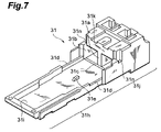
- FIG. 7 is a partial perspective view showing the lower casing 31 .
- the mounting surface 31 i of the lower casing 31 has a projection 31 e matching the substrate supporting portion 14 of the block 10 .
- the projection 31 e comes into contact with a lower portion of the substrate supporting portion 14 , i.e., a surface 13 e positioned under the substrate supporting portion 14 pf the center wall 13 b in FIG. 3B .
- the projection 31 e and the surface 13 e of the block 10 come into contact with each other, thereby positioning the block 10 with respect to the lower casing 31 . Namely, the block 10 is secured between one end part 31 k of the receptacle 31 j and the projection 31 e.
- the optical sub-assembly 21 and circuit board 20 secured to the block 10 are also positioned with respect to the lower casing 31 .
- FIGS. 8A , 8 B, and 8 C are views showing a process of inserting the assembly 44 into the lower casing 31 . These drawings do not depict the second substrate 20 b and the flexible substrate 20 c .
- the assembly 44 is obliquely inserted into the lower casing 31 such that the optical sub-assembly 21 is inserted into the openings 31 m of the receptacle 31 j from the inside.
- the circuit board 20 is moved toward the mounting surface 30 i such that the circuit board 20 becomes parallel to the lower face of the lower casing 31 as shown in FIG. 8B .
- the block 10 is formed with abutting surfaces 16 a to 16 d for bringing the block 10 into contact with the lower casing 31 without any gap.
- the first abutting surface 16 a is formed between the two openings 12 a , 12 b of the front wall 12 .
- the first abutting surface 16 a is disposed so as to come into contact with the rear end part 31 k of the receptacle 31 j.
- the second abutting surfaces 16 b are formed at the front wall 12 so as to project sideways therefrom.
- the third abutting surfaces 16 c are formed at the front wall 12 so as to project downward therefrom.
- the fourth abutting surfaces 16 d are formed at the respective bottom faces of the outer walls 13 a and 13 c so as to project downward therefrom.
- the second abutting surfaces 16 b come into contact with the side walls 31 b of the lower casing 31 . As a consequence, the block 10 is held between a pair of side walls 31 b.
- the third abutting surfaces 16 c come into contact with the bottom face 31 c of the lower casing 31
- the fourth abutting surfaces 16 d come into contact with edge portions 31 d of the lower casing 31 , whereby the block 10 is stably held by the lower casing 31 .
- FIG. 9 is a partial perspective view showing the upper casing 37 .
- the upper casing 37 constitutes an outer case of the optical module 1 .
- the first substrate 20 a is held between the upper casing 37 and lower casing 31 , whereas the second substrate 20 b is mounted thereon.
- engagement structures 37 a to 37 d are formed on each side of the upper casing 37 .
- both side walls 13 a , 13 c of the block 10 have respective cutouts.
- the protrusions 37 a are inserted into these cutouts, and press the block 10 .
- the surfaces 37 b , 37 c of the protrusions 37 a come into contact with the surfaces 12 d , 12 e of the block 10 exposed at the cutouts, thereby determining the positions of the block 10 and upper casing 37 with respect to each other in one direction.
- both side walls of the lower casing 31 have respective engagement structures 31 n as cutting out these side walls.
- the engagement structures 37 d of the upper casing 37 engage their corresponding engagement structures 31 n of the lower casing 31 , thereby positioning the upper casing 37 and the lower casing 31 with respect to each other.
- the lower casing 31 is covered with the cover 32 , whereby the optical module 1 is completed.
- FIG. 11 is an exploded perspective view of the optical module 1 a of the second embodiment.
- the optical module la comprises a block 10 , a transmitting optical sub-assembly 21 a and a receiving optical sub-assembly 21 b (collectively referred to as “optical sub-assembly 21 ”), a first substrate 20 a and a second substrate 20 b (collectively referred to as “circuit board 20 ”) which are used for driving the optical sub-assembly 21 , a housing 30 for enclosing the optical sub-assembly 21 and circuit board 20 , holders 19 , brackets 33 , a shield 34 , an actuator 39 , a fin 38 , and heat transfer sheets 40 , 42 .
- the optical module 1 a differs from that of the structure embodiment in the form of the upper casing.
- the positioning part 54 e comes into contact with the surface 12 g of the front wall 12 exposed at the cutout formed in the center wall 13 b of the block 10 .
- This can define mutual positional relationships between the block 10 , upper casing 54 , and lower casing 31 together with engagement structures 54 a to 54 d provided at both side walls of the upper casing 54 , cutout structures formed in both side walls 13 a , 13 c of the block 10 , and cutout structures 31 n formed in both side walls of the lower casing 31 .
- the optical modules 1 , 1 a in accordance with the foregoing embodiments can position the optical sub-assembly 21 and circuit board 20 before mounting them to the lower casing 31 . Therefore, the optical sub-assembly 21 and the circuit board 20 can efficiently be fixed to each other on the outside of the housing 30 .
- each of the optical modules 1 and 1 a can be assembled easily.
- the holders 19 are provided as a positioning member, so that the optical sub-assembly 21 can be secured after being inserted into the openings 12 a , 12 b of the block 10 , whereby the optical sub-assembly 21 can be reliably positioned and fixed to the circuit board 20 .
Abstract
Provided is an optical module which can be efficiently manufactured. The optical module of the present invention comprises a housing having a lower casing, an upper casing, and a cover; an optical sub-assembly; a circuit board; and a block. The lower casing includes a receptacle mating with an optical connector, and a mount. The upper casing engages with the lower casing. The cover covers the upper casing. The optical sub-assembly optically couples with the optical connector in the receptacle. The circuit board is electrically connected to the optical sub-assembly and mounted to the mount of the lower casing. The block is mounted to the lower casing, and defines relative positions of the lower casing, upper casing, optical sub-assembly, and circuit board.
Description
1. Field of the Invention
The present invention relates to an optical module including a positioning member for positioning an optical device and a circuit board formed with a circuit for driving the optical device.
2. Related Background Art
Known is an optical module constituted by a circuit board implemented with an optical sub-assembly and its driving circuit, a signal amplifying circuit, and the like, and a housing enclosing them. This optical module comprises a receptacle for receiving an optical connector provide data leading end of an optical fiber, whereby optical coupling is achieved between the optical sub-assembly and the optical connector within the receptacle. For optical coupling, the position of the optical sub-assembly must be determined with respect to the optical connector. For positioning the optical sub-assembly with respect to the receptacle, conventional optical modules form the receptacle with an opening for inserting the optical sub-assembly and insert the optical device into the opening, while defining the shape of the receptacle such that the relative position of the optical connector is determined with respect to the opening, whereby optical coupling is achieved between them (see, for example, U.S. Pat. No. 6,335,869).
However, assembly efficiency is inferior in the method comprising the steps of separately setting the optical sub-assemblies 62 and the circuit board 63 into the housing 61 and then bonding them to each other.
Therefore, it is an object of the present invention to provide an optical module having an efficient assembling procedure.
The optical module in accordance with one aspect of the present invention comprises a housing having a lower casing including a receptacle to mate with an optical connector, and a mount, an upper casing to engage the lower casing, and a cover for covering the upper casing; an optical sub-assembly optically coupling with the optical connector in the receptacle; a circuit board electrically connected to the optical sub-assembly and mounted on the mount of the lower casing; and a block, mounted on the lower casing, for defining relative positions of the lower casing, upper casing, optical sub-assembly, and circuit board.
According to the present invention, the block can position the circuit board and optical sub-assembly, whereby the circuit board and the optical sub-assembly can be positioned with respect to the upper and lower casings together with the block. Hence, prior to the completion of assembling, the circuit board and the optical sub-assembly can be fixed to each other in the final positional relationship, thus providing an optical module with efficient assembling.
The optical module in accordance with another aspect comprises an optical sub-assembly mounted with an optical device; a circuit board electrically connected to the optical sub-assembly; a lower casing having a receptacle for receiving an optical connector holding an optical fiber, and a mount for mounting the circuit board; an upper casing to engage the lower casing; and a resin block for defining positions of the optical sub-assembly, circuit board, lower casing, and upper casing. The receptacle includes an abutting surface having an opening for receiving one end of the optical sub-assembly. The block comprises a front wall including one surface, in contact with the abutting surface, having an opening corresponding to the opening of the receptacle and receiving one end of the optical sub-assembly; a center wall; and a pair of side walls disposing the center wall therebetween. The center wall has a supporting portion for holding the circuit board. Each of the pair of side walls has a pressing portion for pressing the circuit board. Holding the circuit board between the supporting portion and pressing portions defines relative positions of the block and circuit board. The mount in the lower casing provides a projection. The block is held between one side face of the projection and the abutting surface. A side wall of the block provides a first cutout. A side wall of the lower casing provides a second cutout. The upper casing is formed with first and second protrusions. The first and second cutouts engage with the first and second protrusions, respectively, thereby defining relative positions of the lower casing, upper casing, and block.
According to this aspect, inserting the optical sub-assembly into the opening of the front wall and holding the circuit board between the supporting portion and pressing portions can position the optical sub-assembly and circuit board with respect to the block. Therefore, before being assembled into the casings, the circuit board and the optical sub-assembly can be fixed to each other in the final positional relationship within the casings. Also, holding the block between the abutting surface of the receptacle and the projection in the lower casing can easily position the block with respect to the lower casing. Further, causing the first and second cutouts to engage with the first and second protrusions, respectively, can easily determine the relative positions of the lower casing, upper casing, and block. Hence, an optical module with easily assembled configuration.
The optical module in accordance with still another aspect comprises an optical sub-assembly having an optical device; a circuit board electrically connected to the optical sub-assembly; a lower casing having a receptacle for receiving an optical connector holding an optical fiber, and a mount for mounting the circuit board; an upper casing to engage with the lower casing; and a resinblock for defining positions of the optical sub-assembly, circuit board, lower casing, and upper casing. The receptacle includes an abutting surface having an opening for receiving one end of the optical sub-assembly. The block comprises a front wall including one surface, in contact with the abutting surface, having an opening corresponding to the opening of the receptacle and receiving one end of the optical sub-assembly; a center wall; and a pair of side walls disposing the center wall therebetween. The center wall has a supporting portion for holding the circuit board. Each of the pair of side walls has a pressing portion for pressing the circuit board. Holding the circuit board between the supporting portion and pressing portions defines relative positions of the block and circuit board. An inner face of the upper casing provides a projection. The center wall of the block provides a cutout. One surface of the proof section and one surface of the cutout of the center wall come into contact with each other, whereby the block is held between the projection and the abutting surface of the receptacle. A side wall of the block provides a first cutout. A side wall of the lower casing provides a second cutout. The upper casing provides first and second protrusions. The first and second cutouts engage with the first and second protrusions, respectively, thereby defining relative positions of the lower casing, upper casing, and block.
According to this aspect, inserting the optical sub-assembly into the opening of the front wall and holding the circuit board between the supporting portion and pressing portions can position the optical sub-assembly and circuit board with respect to the block. Therefore, before being assembled in the casings, the circuit board and the optical sub-assembly can be fixed to each other in the final positional relationship within the casings. Also, holding the block between the abutting surface of the receptacle in the lower casing and the projection in the upper casing can easily position the block with respect to the lower casing. Further, engaging the first and second cutouts with the first and second protrusions, respectively, can easily determine the relative positions of the lower casing, upper casing, and block. Hence, an optical module which can be easily assembled is provided.
In the following, preferred embodiments of the positioning member and optical module of the present invention will be explained in detail with reference to the drawings. In the explanation, elements identical to each other will be referred to with numerals identical to each other without overlapping descriptions.
The optical module 1 of a first embodiment of the present invention will be explained. FIG. 1 is an exploded perspective view of the optical module 1, whereas FIG. 2 is a perspective view of the optical module 1. The optical module 1 comprises a transmitting optical sub-assembly 21 a and a receiving optical sub-assembly 21 b (collectively referred to as “optical sub-assembly 21”), a circuit board 20 on which is formed a circuit for driving the optical sub-assembly 21, and a housing 30 for encasing the optical sub-assembly 21 and circuit board 20. The optical sub-assembly 21 and the circuit board 20 are electrically connected to each other by leads extending from the optical sub-assembly 21.
The housing 30 comprises a lower casing 31 for receiving the optical sub-assembly 21 and circuit board 20, an upper casing 37, and a cover 32 for covering the lower casing 31 and upper casing 37.
The lower casing 31 has a mount 31 h for mounting the block 10, including a mounting surface 31 i for mounting the circuit board 20, and a receptacle 31 j disposed at one end of the mount 31 h.
The receptacle 31 j has openings 31 m. Each opening 31 m receives a leading end of the optical sub-assembly 21. An optical fiber held by an optical connector inserted into the receptacle 31 j from the other end is optically coupled to the optical sub-assembly 21 within the opening 31 m. In this embodiment, the receptacle 31 j is formed with two openings 31 m for receiving the transmitting optical sub-assembly 21 a and receiving optical sub-assembly 21 b, respectively.
The transmitting optical sub-assembly 21 a and the receiving optical sub-assembly 21 b are inserted into the openings 31 m formed in the lower casing 31, whereas the circuit board 20 mounted on the mount 31 h of the lower casing 31 is stopped by a substrate stopper 36, whereby the optical sub-assembly 21 and circuit board 20 are secured to the lower casing 31.
The circuit board 20 comprises a first substrate 20 a and a second substrate 20 b. The first substrate 20 a and second substrate 20 b are connected to each other by a flexible substrate 20 c. When the circuit board 20 is assembled in the housing 30, the flexible substrate 20 c is bent such that the first substrate 20 a and second substrate 20 b faces each other. This can realize a two-story structure as shown in FIG. 2 .
The optical module 1 includes a block 10 for positioning the optical sub-assembly 21 and circuit board 20, and holders 19 for securing the optical sub-assembly 21 with respect to the block 10. The optical module 1 also includes brackets 33 and a shield 34 which are used for reducing noise affecting the optical sub-assembly 21. The optical module 1 further includes a cap 35 attached to an end portion opposite from the receptacle 31 j of the lower casing 31, a fin 38, and an actuator 39 for releasing the engagement with a host board to which the optical module 1 is mounted.
Specifically, the brackets 33 are attached to the outer surface of the optical sub-assembly 21. The shield 34 has a substantially planar shape and has holes through which end portions of the optical sub-assembly 21 can pass. The shield 34 is attached to one surface of the block 10 which will be explained later.
The fin 38 transmits the heat generated by the transmitting optical sub-assembly 21 a itself to the outside of the optical module 1. One end 38 a of the fin 38 is disposed at the outer surface of the transmitting optical sub-assembly 21 a, whereas the other end 38 b is in contact with the upper face of the receptacle 31 j. For enhancing adhesion to the transmitting optical sub-assembly 21 a, a silicone sheet 40 is attached to one end 38 a. For enhancing thermal conductivity, the silicone sheet 40 may contain metal fillers.
The mount 11 is divided into a first region 11 a for mounting the transmitting optical sub-assembly 21 a, and a second region 11 b for mounting the receiving optical sub-assembly 21 b.
The front wall 12 is formed with openings 12 a, 12 b into which respective head portions of the transmitting optical sub-assembly 21 a and receiving optical sub-assembly 21 b placed on the mount 11 can be inserted. Each of the transmitting optical sub-assembly 21 a and receiving optical sub-assembly 21 b has a substantially cylindrical form. The transmitting optical sub-assembly 21 a and receiving optical sub-assembly 21 b have respective flanges 21 d, 21 e, which come into contact with the front wall 12.
The first region 11 a and second region 11 b of the mount 11 have respective cutouts 11 c, 11 d. Since the mount 11 has cutouts 11 c, 11 d, the optical sub-assembly 21 is stably placed on the mount 11. The mount 11 has a semicircular cross section so as to conform to the outer shape of the optical sub-assembly 21.
The side wall 13 is constituted by a pair of outer walls 13 a and 13 c, and a center wall 13 b formed therebetween for partitioning the first region 11 a and second region 11 b.
A portion of an end face of the center wall 13 b projects, so as to form the substrate supporting portion 14. The circuit board 20 is to be positioned on the substrate supporting portion 14. End faces of the outer walls 13 a and 13 c partly project, thereby forming substrate pressing portions 15 a and 15 b. The rear face of the circuit board 20 is supported by the substrate supporting portion 14, whereas its front face is pressed by the substrate pressing portions 15 a, 15 b, whereby the circuit board 20 is positioned.
A method of assembling the optical module 1 will be now explained. First, the transmitting optical sub-assembly 21 a and receiving optical sub-assembly 21 b are inserted into the openings 12 a, 12 b formed in the front wall 12 of the block 10, and are pressed against and secured to the front wall 12 by the holders 19. Subsequently, the circuit board 20 is inserted between the substrate supporting portion 14 and substrate pressing portions 15 a, 15 b of the block 10.
Then, the optical sub-assembly 21 and circuit board 20 positioned by the block 10 are set to a jig 50 as shown in FIG. 5A . Thereafter, the jig 50 is covered with a cover 52 as shown in FIG. 5B , and leads of the optical sub-assembly 21 and the circuit board 20 are connected to each other with solder. Here, the brackets 33 are also attached to the optical sub-assembly 21. FIG. 6 shows an assembly 44 manufactured by the foregoing process. This drawing does not depict the second substrate 20 b and the flexible substrate 20 c.
Subsequently, the assembly 44 is set in the lower casing 31. FIG. 7 is a partial perspective view showing the lower casing 31. The mounting surface 31 i of the lower casing 31 has a projection 31 e matching the substrate supporting portion 14 of the block 10.
The projection 31 e comes into contact with a lower portion of the substrate supporting portion 14, i.e., a surface 13 e positioned under the substrate supporting portion 14 pf the center wall 13 b in FIG. 3B .
The projection 31 e and the surface 13 e of the block 10 come into contact with each other, thereby positioning the block 10 with respect to the lower casing 31. Namely, the block 10 is secured between one end part 31 k of the receptacle 31 j and the projection 31 e.
Since the block 10 is thus positioned with respect to the lower casing 31, the optical sub-assembly 21 and circuit board 20 secured to the block 10 are also positioned with respect to the lower casing 31.
After the optical sub-assembly 21 is inserted into the openings 31 m, the circuit board 20 is moved toward the mounting surface 30 i such that the circuit board 20 becomes parallel to the lower face of the lower casing 31 as shown in FIG. 8B .
Thereafter, the projection 31 e of the lower casing 31 and the surface 13 e of the center wall 13 b of the block 10 are brought into contact with each other, so as to position and secure the optical sub-assembly 21 (see FIG. 8C ).
Here, as shown in FIG. 3B , the block 10 is formed with abutting surfaces 16 a to 16 d for bringing the block 10 into contact with the lower casing 31 without any gap.
The first abutting surface 16 a is formed between the two openings 12 a, 12 b of the front wall 12. The first abutting surface 16 a is disposed so as to come into contact with the rear end part 31 k of the receptacle 31 j.
The second abutting surfaces 16 b are formed at the front wall 12 so as to project sideways therefrom.
The third abutting surfaces 16 c are formed at the front wall 12 so as to project downward therefrom. The fourth abutting surfaces 16 d are formed at the respective bottom faces of the outer walls 13 a and 13 c so as to project downward therefrom.
When the assembly 44 is set in the lower casing 31, the first abutting surface 16 a comes into contact with the partition 31 a between the two openings (see FIG. 7 ).
The second abutting surfaces 16 b come into contact with the side walls 31 b of the lower casing 31. As a consequence, the block 10 is held between a pair of side walls 31 b.
The third abutting surfaces 16 c come into contact with the bottom face 31 c of the lower casing 31, whereas the fourth abutting surfaces 16 d come into contact with edge portions 31 d of the lower casing 31, whereby the block 10 is stably held by the lower casing 31.
Subsequently, the upper casing 37 is put on the lower casing 31 mounted with the assembly 44. FIG. 9 is a partial perspective view showing the upper casing 37.
The upper casing 37 constitutes an outer case of the optical module 1. The first substrate 20 a is held between the upper casing 37 and lower casing 31, whereas the second substrate 20 b is mounted thereon.
As shown in FIG. 9 , engagement structures 37 a to 37 d are formed on each side of the upper casing 37. As shown in FIGS. 3A and 3B , both side walls 13 a, 13 c of the block 10 have respective cutouts. The protrusions 37 a are inserted into these cutouts, and press the block 10. The surfaces 37 b, 37 c of the protrusions 37 a come into contact with the surfaces 12 d, 12 e of the block 10 exposed at the cutouts, thereby determining the positions of the block 10 and upper casing 37 with respect to each other in one direction.
As shown in FIG. 7 , on the other hand, both side walls of the lower casing 31 have respective engagement structures 31 n as cutting out these side walls. The engagement structures 37 d of the upper casing 37 engage their corresponding engagement structures 31 n of the lower casing 31, thereby positioning the upper casing 37 and the lower casing 31 with respect to each other.
After the upper casing 37 is thus put on, the lower casing 31 is covered with the cover 32, whereby the optical module 1 is completed.
The optical module 1 a in accordance with a second embodiment will now be explained. FIG. 11 is an exploded perspective view of the optical module 1 a of the second embodiment. As shown in FIG. 11 , the optical module la comprises a block 10, a transmitting optical sub-assembly 21 a and a receiving optical sub-assembly 21 b (collectively referred to as “optical sub-assembly 21”), a first substrate 20 a and a second substrate 20 b (collectively referred to as “circuit board 20”) which are used for driving the optical sub-assembly 21, a housing 30 for enclosing the optical sub-assembly 21 and circuit board 20, holders 19, brackets 33, a shield 34, an actuator 39, a fin 38, and heat transfer sheets 40, 42. The optical module 1 a differs from that of the structure embodiment in the form of the upper casing.
The positioning part 54 e comes into contact with the surface 12 g of the front wall 12 exposed at the cutout formed in the center wall 13 b of the block 10. This can define mutual positional relationships between the block 10, upper casing 54, and lower casing 31 together with engagement structures 54 a to 54 d provided at both side walls of the upper casing 54, cutout structures formed in both side walls 13 a, 13 c of the block 10, and cutout structures 31 n formed in both side walls of the lower casing 31.
By using the block 10, the optical modules 1, 1 a in accordance with the foregoing embodiments can position the optical sub-assembly 21 and circuit board 20 before mounting them to the lower casing 31. Therefore, the optical sub-assembly 21 and the circuit board 20 can efficiently be fixed to each other on the outside of the housing 30.
Since the block 10 itself can be assembled in the lower casing 31 with the optical sub-assembly 21 and circuit board 20 in the state where the optical sub-assembly 21 and circuit board 20 are positioned with respect to each other, each of the optical modules 1 and 1 a can be assembled easily.
In the foregoing embodiments, the holders 19 are provided as a positioning member, so that the optical sub-assembly 21 can be secured after being inserted into the openings 12 a, 12 b of the block 10, whereby the optical sub-assembly 21 can be reliably positioned and fixed to the circuit board 20.
Claims (11)
1. An optical module comprising:
a housing having a lower easing integrating with a receptacle and a mount, an upper easing engaged with the lower casing, and a cover for covering the upper casing;
a block mounted on the lower casing, the block including a center wall and a pair of side walls disposing the center wall therebetween and a mounting portion, the center wall providing a substrate supporting portion and each of the pair of side walls providing a substrate pressing portion;
a optical sub-assembly mounted on the block and optically coupled with an optical connector mated with the receptacle; and
a substrate mounted on the mount of the lower casing and supported by the block, the substrate being electrically connected to the optical sub-assembly,
wherein the block supports the optical subassembly in the mounting portion and the substrate by sandwiching between the substrate supporting portion and the substrate pressing portion to define relative positions between the block, the optical sub-assembly and the substrate.
2. The optical module according to claim 1 , wherein the block is made of a resin.
3. An optical module comprising:
a housing having a lower casing integrating with a receptacle and a mount, an upper casing engaged with the lower casing, and a cover for covering the upper casing;
a block mounted on the lower casing and including a mounting portion;
an optical sub-assembly mounted on the mounting portion and optically coupled with an optical connector mated with the receptacle; and
a substrate mounted on the mount of the lower casing and supported by the block, the substrate being electrically connected with the optical sub-assembly,
wherein the receptacle has a surface with an opening for abutting against a surface of the block with an opening corresponding to the opening provided in the surface of the receptacle, the optical sub-assembly being inserted into the opening of the surface of the receptacle and the opening of the block, and
wherein the lower casing has a projection on the mount for holding the block between a side face of the projection and the surface of the receptacle such that the surface of the block abuts against the surface of the receptacle.
4. The optical module according to claim 3 , wherein the block provides a first cutout, the lower casing provides a second cutout, and the upper casing provides first and second protrusions for engaging with the first and second cutouts, respectively such that the surface of the block abuts against the surface of the receptacle.
5. The optical module according to claim 4 ,
wherein the block includes a center wall and a pair of side walls, the side walls disposing the center wall therebetween providing the first cutout, the mounting portion being disposed between the center wall and one of side walls.
6. The optical module according to claim 4 , wherein the second cutout is formed in a side wall of the lower casing.
7. The optical module according to claim 3 ,
wherein the upper casing includes a projection and the block includes a center wall with a cutout,
the projection being in contact with a cross section of the cutout such that the surface of the block abuts against the surface of the receptacle.
8. The optical module according to claim 3 ,
further comprising a holder for holding the optical sub-assembly by surrounding the optical sub-assembly and pressing the optical sub-assembly to the block.
9. The optical module according to claim 3 ,
wherein the block is made of a resin.
10. An optical module comprising:
an optical sub-assembly having leads and mounted with an optical device;
a substrate electrically connected to the leads of the optical sub-assembly;
a resin block including a front wall with an opening to insert one end of the optical sub-assembly thereinto, a center wall with a substrate supporting portion and a first cutout, and a pair of side walls disposing the center wall therebetween, each of the side walls providing a substrate pressing portion for pressing the substrate and a second cutout, the substrate supporting portion and the substrate pressing portion fixing the substrate by sandwiching the substrate therebetween;
a lower cashing building with a receptacle and a mount receiving an optical connector holding an optical fiber and providing a surface with an opening for inserting the one end of the optical sub-assembly thereinto, the mount mounting the substrate and providing a projection for sandwiching the block with the surface of the receptacle such that the front wall of the block abuts against the surface of the receptacle, the lower casing providing a third cutout in a side wall thereof; and
an upper casing providing a first protrusion to engage with the first cutout provided in the side wall of the resin block, a second protrusion to engage with the third cutout provided in the side wall of the lower casing, and a third protrusion to engage with the second cutout provided in the center wall of the resin block such that the front wall of the resin block abuts against the surface of the receptacle.
11. A method for manufacturing an optical module including an optical sub-assembly, a block, a substrate, a lower casing and an upper casing, the method comprising steps of:
(a) mounting the optical sub-assembly on the block such that a leading end of the optical sub-assembly is inserted into an opening provided in a front wall of the block;
(b) securing the substrate to the block such that a substrate supporting portion provided in the block and a substrate pressing portion provided in the block sandwiches the substrate therebetween;
(c) electrically connecting the substrate with leads of the optical subassembly;
(d) installing the block mounting the optical sub-assembly electrically connected with the substrate in the lower casing including a receptacle such that the leading end of the optical subassembly inserted into the opening of the block enters an opening formed in a surface of the receptacle; and
(e) assembling the upper casing with the lower casing such that the front wall of the block abuts against the surface of the receptacle.
Applications Claiming Priority (2)
| Application Number | Priority Date | Filing Date | Title |
|---|---|---|---|
| JPP2002-262006 | 2002-09-06 | ||
| JP2002262006A JP2004103743A (en) | 2002-09-06 | 2002-09-06 | Positioning member, and optical module and its manufacturing method |
Publications (2)
| Publication Number | Publication Date |
|---|---|
| US20040197056A1 US20040197056A1 (en) | 2004-10-07 |
| US7121742B2 true US7121742B2 (en) | 2006-10-17 |
Family
ID=32262202
Family Applications (1)
| Application Number | Title | Priority Date | Filing Date |
|---|---|---|---|
| US10/655,589 Expired - Lifetime US7121742B2 (en) | 2002-09-06 | 2003-09-05 | Optical module |
Country Status (2)
| Country | Link |
|---|---|
| US (1) | US7121742B2 (en) |
| JP (1) | JP2004103743A (en) |
Cited By (5)
| Publication number | Priority date | Publication date | Assignee | Title |
|---|---|---|---|---|
| US20070237466A1 (en) * | 2006-04-05 | 2007-10-11 | Finisar Corporation | Horseshoe spring for securing an optical nosepiece during optical alignment |
| US20100098385A1 (en) * | 2008-10-21 | 2010-04-22 | Nec Corporation | Optical module locking mechanism and method of locking and releasing a locking state of an optical module |
| US20100178013A1 (en) * | 2009-01-09 | 2010-07-15 | Sumitomo Electric Industries, Ltd. | Optical transceiver with partition plate between tosa and rosa |
| US8672562B2 (en) | 2010-08-20 | 2014-03-18 | Sumitomo Electric Industries, Ltd. | Optical transceiver having effective heat conducting path from TOSA to metal housing |
| US20190391349A1 (en) * | 2018-06-20 | 2019-12-26 | Hisense Broadband Multimedia Technologies Co., Ltd. | Optical module |
Families Citing this family (18)
| Publication number | Priority date | Publication date | Assignee | Title |
|---|---|---|---|---|
| US7201520B2 (en) * | 2003-05-30 | 2007-04-10 | Sumitomo Electric Industries, Ltd. | Optical module having a simple mechanism for releasing from a cage |
| US20050254757A1 (en) * | 2004-02-23 | 2005-11-17 | Ferretti Vincent E Iii | Connector port for network interface device |
| JP2005316475A (en) * | 2004-04-29 | 2005-11-10 | Sumitomo Electric Ind Ltd | Optical transceiver |
| JP2006171398A (en) | 2004-12-16 | 2006-06-29 | Hitachi Cable Ltd | Optical transmission module |
| JP4403964B2 (en) * | 2004-12-28 | 2010-01-27 | 日立電線株式会社 | Optical transceiver |
| JP4466517B2 (en) | 2005-09-13 | 2010-05-26 | 日立電線株式会社 | Optical transceiver |
| JP4932303B2 (en) * | 2006-03-29 | 2012-05-16 | 住友電工デバイス・イノベーション株式会社 | Optical communication module and manufacturing method thereof |
| JP2009152473A (en) * | 2007-12-21 | 2009-07-09 | Icom Inc | Fitting structure of light-emitting diode element |
| US9052477B2 (en) | 2009-10-29 | 2015-06-09 | Sumitomo Electric Industries, Ltd. | Optical transceiver with inner fiber set within tray securing thermal path from electronic device to housing |
| JP5471787B2 (en) * | 2010-04-30 | 2014-04-16 | 住友電気工業株式会社 | Optical transceiver |
| WO2011052802A2 (en) | 2009-10-29 | 2011-05-05 | Sumitomo Electric Industries, Ltd. | Pluggable optical transceiver and method for manufacturing the same |
| US8821039B2 (en) | 2009-10-29 | 2014-09-02 | Sumitomo Electric Industries, Ltd. | Optical transceiver having optical receptacle arranged diagonally to longitudinal axis |
| US8967884B2 (en) | 2010-12-14 | 2015-03-03 | Sumitomo Electric Industries, Ltd. | Optical transceiver |
| US8380073B2 (en) * | 2011-05-24 | 2013-02-19 | Sumitomo Electric Industries, Ltd. | Optical transceiver implemented with tunable LD |
| US8500342B2 (en) * | 2011-07-21 | 2013-08-06 | Avago Technologies General Ip (Singapore) Pte. Ltd. | Opto-electronic communication module having retainer for aligning optical ports |
| US9638876B2 (en) | 2013-08-02 | 2017-05-02 | Fci Americas Technology Llc | Opto-electrical transceiver module and active optical cable |
| EP3121630B1 (en) * | 2015-07-21 | 2023-04-05 | Tyco Electronics Svenska Holdings AB | Optoelectronic module with improved heat management |
| CN110865441B (en) * | 2018-08-27 | 2021-11-19 | 苏州旭创科技有限公司 | Optical module |
Citations (14)
| Publication number | Priority date | Publication date | Assignee | Title |
|---|---|---|---|---|
| JPS61149129A (en) | 1984-12-24 | 1986-07-07 | 株式会社東芝 | Ultrasonic diagnostic apparatus |
| JPH0217862A (en) | 1988-07-01 | 1990-01-22 | Fujitsu Ltd | Series resonance converter |
| JPH05291693A (en) | 1992-04-06 | 1993-11-05 | Mitsubishi Electric Corp | Method of heat removal for semiconductor laser |
| JP2001091795A (en) | 1999-07-19 | 2001-04-06 | Furukawa Electric Co Ltd:The | Receptacle module |
| US6335869B1 (en) | 2000-01-20 | 2002-01-01 | International Business Machines Corporation | Removable small form factor fiber optic transceiver module and electromagnetic radiation shield |
| JP2002015450A (en) | 2000-06-29 | 2002-01-18 | Sanyo Electric Co Ltd | Optical pickup device |
| US6445475B1 (en) | 1998-06-02 | 2002-09-03 | Sony Corporation | Method for practically loading transmission or receiving module for optical link and its rigid flexible board |
| US20020154362A1 (en) | 2001-03-27 | 2002-10-24 | Kazushige Oki | Optical link module |
| US20030063424A1 (en) | 2001-09-28 | 2003-04-03 | Sumitomo Electric Industries, Ltd. | Optical module |
| US6556445B2 (en) * | 2000-11-30 | 2003-04-29 | Raul Medina | Transceiver module with extended release lever |
| US6600611B2 (en) | 2001-09-28 | 2003-07-29 | Sumitomo Electric Industries, Ltd. | Optical module |
| US6830383B2 (en) * | 2001-10-17 | 2004-12-14 | Hon Hai Precision Ind. Co., Ltd | Small form factor pluggable optoelectronic transceiver module |
| US6863448B2 (en) * | 2001-04-14 | 2005-03-08 | Jds Uniphase Corporation | Method and apparatus for push button release fiber optic modules |
| US6893168B2 (en) * | 2001-10-12 | 2005-05-17 | Hon Hai Precision Ind. Co., Ltd. | Optical transceiver module with multiple grounding paths |
-
2002
- 2002-09-06 JP JP2002262006A patent/JP2004103743A/en active Pending
-
2003
- 2003-09-05 US US10/655,589 patent/US7121742B2/en not_active Expired - Lifetime
Patent Citations (14)
| Publication number | Priority date | Publication date | Assignee | Title |
|---|---|---|---|---|
| JPS61149129A (en) | 1984-12-24 | 1986-07-07 | 株式会社東芝 | Ultrasonic diagnostic apparatus |
| JPH0217862A (en) | 1988-07-01 | 1990-01-22 | Fujitsu Ltd | Series resonance converter |
| JPH05291693A (en) | 1992-04-06 | 1993-11-05 | Mitsubishi Electric Corp | Method of heat removal for semiconductor laser |
| US6445475B1 (en) | 1998-06-02 | 2002-09-03 | Sony Corporation | Method for practically loading transmission or receiving module for optical link and its rigid flexible board |
| JP2001091795A (en) | 1999-07-19 | 2001-04-06 | Furukawa Electric Co Ltd:The | Receptacle module |
| US6335869B1 (en) | 2000-01-20 | 2002-01-01 | International Business Machines Corporation | Removable small form factor fiber optic transceiver module and electromagnetic radiation shield |
| JP2002015450A (en) | 2000-06-29 | 2002-01-18 | Sanyo Electric Co Ltd | Optical pickup device |
| US6556445B2 (en) * | 2000-11-30 | 2003-04-29 | Raul Medina | Transceiver module with extended release lever |
| US20020154362A1 (en) | 2001-03-27 | 2002-10-24 | Kazushige Oki | Optical link module |
| US6863448B2 (en) * | 2001-04-14 | 2005-03-08 | Jds Uniphase Corporation | Method and apparatus for push button release fiber optic modules |
| US20030063424A1 (en) | 2001-09-28 | 2003-04-03 | Sumitomo Electric Industries, Ltd. | Optical module |
| US6600611B2 (en) | 2001-09-28 | 2003-07-29 | Sumitomo Electric Industries, Ltd. | Optical module |
| US6893168B2 (en) * | 2001-10-12 | 2005-05-17 | Hon Hai Precision Ind. Co., Ltd. | Optical transceiver module with multiple grounding paths |
| US6830383B2 (en) * | 2001-10-17 | 2004-12-14 | Hon Hai Precision Ind. Co., Ltd | Small form factor pluggable optoelectronic transceiver module |
Cited By (7)
| Publication number | Priority date | Publication date | Assignee | Title |
|---|---|---|---|---|
| US20070237466A1 (en) * | 2006-04-05 | 2007-10-11 | Finisar Corporation | Horseshoe spring for securing an optical nosepiece during optical alignment |
| US7559704B2 (en) * | 2006-04-05 | 2009-07-14 | Finisar Corporation | Horseshoe spring for securing an optical nosepiece during optical alignment |
| US20100098385A1 (en) * | 2008-10-21 | 2010-04-22 | Nec Corporation | Optical module locking mechanism and method of locking and releasing a locking state of an optical module |
| US20100178013A1 (en) * | 2009-01-09 | 2010-07-15 | Sumitomo Electric Industries, Ltd. | Optical transceiver with partition plate between tosa and rosa |
| US8226304B2 (en) * | 2009-01-09 | 2012-07-24 | Sumitomo Electric Industries, Ltd. | Optical transceiver with partition plate between TOSA and ROSA |
| US8672562B2 (en) | 2010-08-20 | 2014-03-18 | Sumitomo Electric Industries, Ltd. | Optical transceiver having effective heat conducting path from TOSA to metal housing |
| US20190391349A1 (en) * | 2018-06-20 | 2019-12-26 | Hisense Broadband Multimedia Technologies Co., Ltd. | Optical module |
Also Published As
| Publication number | Publication date |
|---|---|
| JP2004103743A (en) | 2004-04-02 |
| US20040197056A1 (en) | 2004-10-07 |
Similar Documents
| Publication | Publication Date | Title |
|---|---|---|
| US7121742B2 (en) | Optical module | |
| US6502998B2 (en) | Optoelectronic transceiver module | |
| JP4189692B2 (en) | Optical module package and optical module | |
| US7347635B2 (en) | Optical transceiver | |
| JP4567386B2 (en) | Lens module mounting method and structure thereof | |
| EP0709699A2 (en) | Optical module having structure for defining fixing position of sleeve | |
| EP0646816A2 (en) | Optical module, method of manufacturing the same, and sleeve | |
| US6619859B1 (en) | Receptacle module | |
| JP4269291B2 (en) | Optical module | |
| US5875047A (en) | Optical transceiver unit | |
| JP2001143797A (en) | Cable connector | |
| US6863451B2 (en) | Optical module | |
| JPH09223552A (en) | Movable connector for board and connector terminal | |
| US20030034498A1 (en) | Light emitting module and the method of the producing the same | |
| US6817775B2 (en) | Optical connector with electromagnetic noise shielding and heat radiating properties | |
| EP1229367A2 (en) | Optical connector and a structure with a mounted connector | |
| JP3938088B2 (en) | Optical communication device | |
| JP4543561B2 (en) | Optical module manufacturing method and optical module | |
| JP2004247700A (en) | Optical module | |
| JP2010008588A (en) | Optical transceiver | |
| JP3803264B2 (en) | Optical transceiver and method for manufacturing optical transceiver | |
| JP2002303766A (en) | Optical connector | |
| JP2004228509A (en) | Packaged module | |
| JPS6320967Y2 (en) | ||
| JPH09159877A (en) | Module for optical link and its assembly |
Legal Events
| Date | Code | Title | Description |
|---|---|---|---|
| AS | Assignment |
Owner name: SUMITOMO ELECTRIC INDUSTRIES, LTD, JAPAN Free format text: ASSIGNMENT OF ASSIGNORS INTEREST;ASSIGNOR:OKI, KAZUSHIGE;REEL/FRAME:015432/0256 Effective date: 20040429 |
|
| STCF | Information on status: patent grant |
Free format text: PATENTED CASE |
|
| FPAY | Fee payment |
Year of fee payment: 4 |
|
| FPAY | Fee payment |
Year of fee payment: 8 |
|
| MAFP | Maintenance fee payment |
Free format text: PAYMENT OF MAINTENANCE FEE, 12TH YEAR, LARGE ENTITY (ORIGINAL EVENT CODE: M1553) Year of fee payment: 12 |