US7126437B2 - Bus signaling through electromagnetic couplers having different coupling strengths at different locations - Google Patents
Bus signaling through electromagnetic couplers having different coupling strengths at different locations Download PDFInfo
- Publication number
- US7126437B2 US7126437B2 US10/165,096 US16509602A US7126437B2 US 7126437 B2 US7126437 B2 US 7126437B2 US 16509602 A US16509602 A US 16509602A US 7126437 B2 US7126437 B2 US 7126437B2
- Authority
- US
- United States
- Prior art keywords
- coupling
- bus
- different
- strengths
- elements
- Prior art date
- Legal status (The legal status is an assumption and is not a legal conclusion. Google has not performed a legal analysis and makes no representation as to the accuracy of the status listed.)
- Expired - Fee Related, expires
Links
- 230000008878 coupling Effects 0.000 title claims abstract description 82
- 238000010168 coupling process Methods 0.000 title claims abstract description 82
- 238000005859 coupling reaction Methods 0.000 title claims abstract description 82
- 230000011664 signaling Effects 0.000 title description 2
- 238000004891 communication Methods 0.000 claims abstract description 5
- 238000004519 manufacturing process Methods 0.000 claims description 9
- 238000000034 method Methods 0.000 claims description 6
- 239000000463 material Substances 0.000 claims description 4
- 125000006850 spacer group Chemical group 0.000 claims description 4
- 230000035699 permeability Effects 0.000 claims description 2
- 230000007246 mechanism Effects 0.000 description 3
- 230000008901 benefit Effects 0.000 description 2
- 230000012447 hatching Effects 0.000 description 2
- 239000002184 metal Substances 0.000 description 2
- 230000004075 alteration Effects 0.000 description 1
- 230000000593 degrading effect Effects 0.000 description 1
- 239000003989 dielectric material Substances 0.000 description 1
- 238000009434 installation Methods 0.000 description 1
- 230000000750 progressive effect Effects 0.000 description 1
Images


Classifications
-
- H—ELECTRICITY
- H01—ELECTRIC ELEMENTS
- H01P—WAVEGUIDES; RESONATORS, LINES, OR OTHER DEVICES OF THE WAVEGUIDE TYPE
- H01P5/00—Coupling devices of the waveguide type
- H01P5/12—Coupling devices having more than two ports
- H01P5/16—Conjugate devices, i.e. devices having at least one port decoupled from one other port
- H01P5/18—Conjugate devices, i.e. devices having at least one port decoupled from one other port consisting of two coupled guides, e.g. directional couplers
- H01P5/184—Conjugate devices, i.e. devices having at least one port decoupled from one other port consisting of two coupled guides, e.g. directional couplers the guides being strip lines or microstrips
- H01P5/185—Edge coupled lines
-
- H—ELECTRICITY
- H04—ELECTRIC COMMUNICATION TECHNIQUE
- H04L—TRANSMISSION OF DIGITAL INFORMATION, e.g. TELEGRAPHIC COMMUNICATION
- H04L12/00—Data switching networks
- H04L12/28—Data switching networks characterised by path configuration, e.g. LAN [Local Area Networks] or WAN [Wide Area Networks]
- H04L12/40—Bus networks
- H04L12/403—Bus networks with centralised control, e.g. polling
-
- H—ELECTRICITY
- H04—ELECTRIC COMMUNICATION TECHNIQUE
- H04L—TRANSMISSION OF DIGITAL INFORMATION, e.g. TELEGRAPHIC COMMUNICATION
- H04L25/00—Baseband systems
- H04L25/02—Details ; arrangements for supplying electrical power along data transmission lines
- H04L25/0264—Arrangements for coupling to transmission lines
- H04L25/0266—Arrangements for providing Galvanic isolation, e.g. by means of magnetic or capacitive coupling
Definitions
- Electromagnetic couplers can be used, for example, to couple data between electronic devices and a communication bus (e.g., a multi-drop bus) in place of more conventional direct electrical connections.
- a communication bus e.g., a multi-drop bus
- Such an arrangement is proposed in U.S. Pat. No. 5,638,402.
- An electronic device that communicates data on a bus sends or receives the data in the form of an electrical signal that conforms to a predefined signaling specification.
- the receiving device In recovering the data from the received signal, the receiving device assumes that the signal conformed to the specification when it was sent.
- FIG. 1 shows a schematic view of a prior art bus.
- FIG. 2 shows a graph of coupling strength
- FIG. 3 shows a schematic view of a bus.
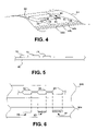
- FIG. 4 shows a coupler on a bus.
- FIGS. 5 and 6 respectively, show a side view and a top view of a portion of a bus.
- the coupling strengths of the couplings between the bus and the communicating devices 24 , 26 , 28 may all be controlled to be uniformly within a targeted range.
- One way to control the coupling strengths to be uniform is to impose tight manufacturing tolerances on the dimensions and properties of dielectric materials associated with the couplings.
- Another is to use zigzag coupler geometries that reduce the impact on coupling strength due to variations in the geometric precision of the coupling arrangements. Zigzag coupling arrangements are described in U.S. Pat. No. 6,573,801.
- Controlling coupling strengths to fall uniformly within a particular range achieves a compromise between competing constraints. Excessive coupler strengths cause large impedance disturbances along the bus, thereby degrading signal integrity. High coupler strengths also divert too much signal energy into drop-off points 24 that are closer to the bus master 30 , leaving little energy to divert to distant drop-off points 28 . On the other hand, insufficient coupler strength causes even the nearest drop-off points to receive or impart too little energy from or to the bus.
- each device along the bus It is useful to arrange for each device along the bus to receive the same amount of energy as any of the other devices along the bus.
- the amount of energy received by a device depends on both the coupling strength and the amount of energy available on the bus at the point of coupling.
- each coupler 42 , 44 , 46 along the length of the bus respectively drains an amount of energy 41 , 43 , 45 from the bus.
- the energy drained by the coupler 42 for example, leaves a smaller remaining amount of energy 47 to reach the next coupler 44 farther from the bus master. Because the amount of energy on the bus at the coupling location of the next coupler, e.g., coupler 44 , is lower, the coupling strength must be higher for coupler 44 to drain the same energy 43 as was drained by the prior coupler 42 .
- coupler 44 The higher coupling strength of coupler 44 is tolerable because there are fewer downstream couplers that need to draw energy from the bus than was the case for coupler 42 . Conversely, weaker earlier couplers are tolerable because the full signal energy is available for them to sample, while the fact that they drain less energy benefits later couplers.
- couplers 91 , 92 , 93 having non-uniform coupling strengths occupy respective coupling locations along a bus 90 .
- the coupler 91 is at the coupling location closest to a bus master 97 and the coupler 93 is at the coupling location furthest from the bus master 97 .
- Devices 94 , 95 , 96 are respectively coupled to the coupling locations for communication on the bus 90 .
- the relative coupling strengths of the couplers 91 , 92 , 93 are shown symbolically in FIG. 3 by drawn lines. Couplers drawn using longer lines, e.g., coupler 93 represent stronger coupling strengths, although physical dimensions are only one way of achieving this.
- coupler material properties of the coupler, for example, permittivity and permeability and the extent of the coupler along all three dimensions.
- the configuration of the traces may also be controlled (patterned). For example, besides zig-zags, perforated ground planes and other implementations may be used.
- Coupler strengths along the bus reduces the cost associated with tight manufacturing tolerances, because couplers having a range of different strengths become useful. Yield increases and cost is reduced.
- a variety of mechanisms may be used for introducing and utilizing non-uniform coupler strengths for multi-drop electromagnetically coupled buses.
- the finished couplers may be tested (e.g., by measuring the coupling strength of each coupler) and sorted by coupling strength.
- the relative coupling strengths of the couplers may be indicated by marking the couplers 56 with color 58 or symbols (e.g., bar code 60 ) or other indicia or devices. Any device or technique can be used which assures that couplers of the intended strength occupy intended positions along the bus.
- the system may rely on human installation in the right position based on color.
- the placing of the couplers may be effected by robotic systems that could “read” color indications or bar codes or other information marked on the couplers.
- appropriate positioning of the various couplers may be enforced by providing different keyed mechanical features 62 on the couplers that correspond to the different coupling strengths.
- the motherboard 64 may then be constructed to have corresponding features 66 to accept only a particular coupler key at each position along the bus 68 .
- coupler strength may be achieved more deliberately, for example, by controlling dielectric thicknesses, dielectric constants, and the number of zigzag geometry crossover points on the coupling traces of the bus and the coupler.
- the choice among possible mechanisms could be based on cost. For example, if the cost of engineering and manufacturing multiple categories of modules to be attached to the bus is a concern, the system may use uniform daughter cards and make alterations only to parameters of the motherboards that affect the coupling strengths at various points along the bus.
- variations of motherboards may include dielectric spacers 70 , 72 , 74 of different heights glued to the motherboard 80 at the locations of drop-off points along the bus. Or the widths of motherboard coupling traces 80 , 82 , 84 may be different at different coupler locations, as shown on FIG. 6 (also not to scale).
- Wider traces would yield stronger coupling for couplers that are farther away from the bus controller. Wider traces could use either different categories of daughter cards (if the trace width variations were to be provided on the daughter cards rather than on the motherboard) or adjustment of the trace widths on the motherboard.
- the variation in impedance of the motherboard traces 82 , 84 , 86 (see FIG. 6 ) in an internal plane 64 b within the motherboard 64 could be offset, if desired, by configuring another internal plane 64 a , e.g., by progressive cross hatching.
- the cross-hatching is in the form of a pattern of holes 88 , 90 , 92 in the ground plane 64 a of the motherboard 64 as best seen in FIG. 6 .
- the removal of metal changes the impedance, because the field lines terminate in different patterns than for continuous metal. More cross hatching may be provided under wider traces.
- the cross-hatching maintains the average overlap between the trace and the ground plane, which factors into the trace impedance, thus removing any unwanted correlation between the strength of a coupler and its standalone impedance to its own ground plane.
Abstract
Description
Claims (15)
Priority Applications (6)
| Application Number | Priority Date | Filing Date | Title |
|---|---|---|---|
| US10/165,096 US7126437B2 (en) | 2002-06-05 | 2002-06-05 | Bus signaling through electromagnetic couplers having different coupling strengths at different locations |
| EP03731491A EP1510053B1 (en) | 2002-06-05 | 2003-05-30 | Method and system for electromagnetically coupling devices to a bus |
| PCT/US2003/017314 WO2003105427A1 (en) | 2002-06-05 | 2003-05-30 | Method and system for electromagnetically coupling devices to a bus |
| CN03818822.8A CN1675905B (en) | 2002-06-05 | 2003-05-30 | Method and system for electromagnetically coupling devices to a bus |
| AU2003240483A AU2003240483A1 (en) | 2002-06-05 | 2003-05-30 | Method and system for electromagnetically coupling devices to a bus |
| TW092115082A TWI224736B (en) | 2002-06-05 | 2003-06-03 | Bus signaling through electromagnetic couplers |
Applications Claiming Priority (1)
| Application Number | Priority Date | Filing Date | Title |
|---|---|---|---|
| US10/165,096 US7126437B2 (en) | 2002-06-05 | 2002-06-05 | Bus signaling through electromagnetic couplers having different coupling strengths at different locations |
Publications (2)
| Publication Number | Publication Date |
|---|---|
| US20030227346A1 US20030227346A1 (en) | 2003-12-11 |
| US7126437B2 true US7126437B2 (en) | 2006-10-24 |
Family
ID=29710359
Family Applications (1)
| Application Number | Title | Priority Date | Filing Date |
|---|---|---|---|
| US10/165,096 Expired - Fee Related US7126437B2 (en) | 2002-06-05 | 2002-06-05 | Bus signaling through electromagnetic couplers having different coupling strengths at different locations |
Country Status (6)
| Country | Link |
|---|---|
| US (1) | US7126437B2 (en) |
| EP (1) | EP1510053B1 (en) |
| CN (1) | CN1675905B (en) |
| AU (1) | AU2003240483A1 (en) |
| TW (1) | TWI224736B (en) |
| WO (1) | WO2003105427A1 (en) |
Cited By (6)
| Publication number | Priority date | Publication date | Assignee | Title |
|---|---|---|---|---|
| US20050251598A1 (en) * | 2002-07-01 | 2005-11-10 | Hideki Osaka | Equal-amplitude signaling directional coupling bus |
| US20060279379A1 (en) * | 2005-06-13 | 2006-12-14 | Gale Robert D | Electric signal splitters |
| US20070287325A1 (en) * | 2002-12-30 | 2007-12-13 | Intel Corporation | Electromagnetic Coupler Registration and Mating |
| US20080150546A1 (en) * | 2005-06-15 | 2008-06-26 | Gale Robert D | Continuity tester adaptors |
| US20080266017A1 (en) * | 2002-06-05 | 2008-10-30 | Intel Corporation | Controlling coupling strength in electromagnetic bus coupling |
| US7808338B1 (en) * | 2009-04-03 | 2010-10-05 | Hon Hai Precision Industry Co., Ltd. | Circuit topology for multiple loads |
Families Citing this family (5)
| Publication number | Priority date | Publication date | Assignee | Title |
|---|---|---|---|---|
| US7075795B2 (en) * | 2002-02-14 | 2006-07-11 | Intel Corporation | Electromagnetic bus coupling |
| US20030152153A1 (en) * | 2002-02-14 | 2003-08-14 | Simon Thomas D. | Signaling through electromagnetic couplers |
| US7068120B2 (en) | 2002-06-25 | 2006-06-27 | Intel Corporation | Electromagnetic bus coupling having an electromagnetic coupling interposer |
| DE102004032513B4 (en) * | 2004-07-06 | 2013-04-04 | Continental Teves Ag & Co. Ohg | Circuit arrangement for contactless tapping of electrical signals from at least one signal line |
| US7342466B2 (en) * | 2005-08-10 | 2008-03-11 | Intel Corporation | Hybrid coupler having resistive coupling and electromagnetic coupling |
Citations (27)
| Publication number | Priority date | Publication date | Assignee | Title |
|---|---|---|---|---|
| US3516065A (en) | 1967-01-13 | 1970-06-02 | Ibm | Digital transmission system |
| US3619504A (en) | 1967-01-13 | 1971-11-09 | Ibm | Directional nonreturn to zero computer bussing system |
| US3673548A (en) | 1970-10-19 | 1972-06-27 | Itt | Printed circuit board connector |
| US5192832A (en) | 1990-08-31 | 1993-03-09 | Amp Incorporated | Electromagnet insert for data current coupler |
| US5363071A (en) * | 1993-05-04 | 1994-11-08 | Motorola, Inc. | Apparatus and method for varying the coupling of a radio frequency signal |
| US5432486A (en) | 1993-05-20 | 1995-07-11 | Northern Telecom Limited | Capacitive and inductive coupling connector |
| US5638402A (en) | 1993-09-27 | 1997-06-10 | Hitachi, Ltd. | Fast data transfer bus |
| US5958030A (en) | 1996-12-27 | 1999-09-28 | Nortel Networks Corporation | Intra-shelf free space interconnect |
| US6111476A (en) * | 1998-12-21 | 2000-08-29 | Nortel Networks Corporation | Non-contact coupling system |
| WO2000072163A1 (en) | 1999-05-25 | 2000-11-30 | High Speed Solutions Corporation | High-speed digital distribution system |
| US6163464A (en) | 1997-08-08 | 2000-12-19 | Hitachi, Ltd. | Apparatus for interconnecting logic boards |
| US20010024888A1 (en) | 1999-05-25 | 2001-09-27 | Marketkar Nandu J. | Electromagnetic coupler socket |
| US20010053187A1 (en) | 1999-05-25 | 2001-12-20 | Simon Thomas D. | Symbol-based signaling device for an elctromagnetically-coupled bus system |
| US6335662B1 (en) * | 1999-09-21 | 2002-01-01 | The United States Of America As Represented By The Secretary Of The Army | Ferroelectric-tunable microwave branching couplers |
| US20020018526A1 (en) | 2000-08-09 | 2002-02-14 | Hideki Osaka | Data transmission system of directional coupling type using forward wave and reflection wave |
| US6399898B1 (en) | 1999-11-18 | 2002-06-04 | Nortel Networks Limited | Technique for coupling signals between circuit boards |
| US6434647B1 (en) | 1999-05-27 | 2002-08-13 | Microsoft Corporation | Reflected-wave bus termination |
| US6438012B1 (en) | 1999-05-12 | 2002-08-20 | Hitachi, Ltd. | Directional coupling memory module |
| US6573801B1 (en) | 2000-11-15 | 2003-06-03 | Intel Corporation | Electromagnetic coupler |
| US6576847B2 (en) * | 1999-05-25 | 2003-06-10 | Intel Corporation | Clamp to secure carrier to device for electromagnetic coupler |
| US20030152153A1 (en) | 2002-02-14 | 2003-08-14 | Simon Thomas D. | Signaling through electromagnetic couplers |
| US20030150642A1 (en) | 2002-02-14 | 2003-08-14 | Yinan Wu | Electromagnetic bus coupling |
| US6625682B1 (en) | 1999-05-25 | 2003-09-23 | Intel Corporation | Electromagnetically-coupled bus system |
| US20030227347A1 (en) | 2002-06-05 | 2003-12-11 | Simon Thomas D. | Controlling coupling strength in electromagnetic bus coupling |
| US20030236005A1 (en) | 2002-06-25 | 2003-12-25 | Yinan Wu | Electromagnetic bus coupling |
| US6705898B2 (en) | 2000-11-07 | 2004-03-16 | Endress + Hauser Conducta Gesellschaft Fur Mess-Und Regeltechnik Mbh +Co. | Connector for connecting a transmission line to at least one sensor |
| US6882239B2 (en) | 2001-05-08 | 2005-04-19 | Formfactor, Inc. | Electromagnetically coupled interconnect system |
Family Cites Families (5)
| Publication number | Priority date | Publication date | Assignee | Title |
|---|---|---|---|---|
| US18526A (en) * | 1857-10-27 | Steam-pressure gkage | ||
| US4192832A (en) * | 1979-01-29 | 1980-03-11 | Goettl Adam D | Automatic flushing and draining reservoir apparatus for evaporative coolers |
| CN2286322Y (en) * | 1996-12-13 | 1998-07-15 | 李曦 | Chromatic circle resistance direct-reading card |
| AUPO546797A0 (en) * | 1997-03-05 | 1997-03-27 | Commonwealth Scientific And Industrial Research Organisation | A high frequency multi-port switching circuit |
| US6437647B1 (en) * | 2001-01-30 | 2002-08-20 | Conexant Systems, Inc. | Current mirror compensation system for power amplifiers |
-
2002
- 2002-06-05 US US10/165,096 patent/US7126437B2/en not_active Expired - Fee Related
-
2003
- 2003-05-30 AU AU2003240483A patent/AU2003240483A1/en not_active Abandoned
- 2003-05-30 WO PCT/US2003/017314 patent/WO2003105427A1/en not_active Application Discontinuation
- 2003-05-30 EP EP03731491A patent/EP1510053B1/en not_active Expired - Lifetime
- 2003-05-30 CN CN03818822.8A patent/CN1675905B/en not_active Expired - Fee Related
- 2003-06-03 TW TW092115082A patent/TWI224736B/en not_active IP Right Cessation
Patent Citations (28)
| Publication number | Priority date | Publication date | Assignee | Title |
|---|---|---|---|---|
| US3516065A (en) | 1967-01-13 | 1970-06-02 | Ibm | Digital transmission system |
| US3619504A (en) | 1967-01-13 | 1971-11-09 | Ibm | Directional nonreturn to zero computer bussing system |
| US3673548A (en) | 1970-10-19 | 1972-06-27 | Itt | Printed circuit board connector |
| US5192832A (en) | 1990-08-31 | 1993-03-09 | Amp Incorporated | Electromagnet insert for data current coupler |
| US5363071A (en) * | 1993-05-04 | 1994-11-08 | Motorola, Inc. | Apparatus and method for varying the coupling of a radio frequency signal |
| US5432486A (en) | 1993-05-20 | 1995-07-11 | Northern Telecom Limited | Capacitive and inductive coupling connector |
| US5638402A (en) | 1993-09-27 | 1997-06-10 | Hitachi, Ltd. | Fast data transfer bus |
| US5958030A (en) | 1996-12-27 | 1999-09-28 | Nortel Networks Corporation | Intra-shelf free space interconnect |
| US6163464A (en) | 1997-08-08 | 2000-12-19 | Hitachi, Ltd. | Apparatus for interconnecting logic boards |
| US6111476A (en) * | 1998-12-21 | 2000-08-29 | Nortel Networks Corporation | Non-contact coupling system |
| US6438012B1 (en) | 1999-05-12 | 2002-08-20 | Hitachi, Ltd. | Directional coupling memory module |
| WO2000072163A1 (en) | 1999-05-25 | 2000-11-30 | High Speed Solutions Corporation | High-speed digital distribution system |
| US6576847B2 (en) * | 1999-05-25 | 2003-06-10 | Intel Corporation | Clamp to secure carrier to device for electromagnetic coupler |
| US20010024888A1 (en) | 1999-05-25 | 2001-09-27 | Marketkar Nandu J. | Electromagnetic coupler socket |
| US20010053187A1 (en) | 1999-05-25 | 2001-12-20 | Simon Thomas D. | Symbol-based signaling device for an elctromagnetically-coupled bus system |
| US6498305B1 (en) | 1999-05-25 | 2002-12-24 | Intel Corporation | Interconnect mechanics for electromagnetic coupler |
| US6625682B1 (en) | 1999-05-25 | 2003-09-23 | Intel Corporation | Electromagnetically-coupled bus system |
| US6434647B1 (en) | 1999-05-27 | 2002-08-13 | Microsoft Corporation | Reflected-wave bus termination |
| US6335662B1 (en) * | 1999-09-21 | 2002-01-01 | The United States Of America As Represented By The Secretary Of The Army | Ferroelectric-tunable microwave branching couplers |
| US6399898B1 (en) | 1999-11-18 | 2002-06-04 | Nortel Networks Limited | Technique for coupling signals between circuit boards |
| US20020018526A1 (en) | 2000-08-09 | 2002-02-14 | Hideki Osaka | Data transmission system of directional coupling type using forward wave and reflection wave |
| US6705898B2 (en) | 2000-11-07 | 2004-03-16 | Endress + Hauser Conducta Gesellschaft Fur Mess-Und Regeltechnik Mbh +Co. | Connector for connecting a transmission line to at least one sensor |
| US6573801B1 (en) | 2000-11-15 | 2003-06-03 | Intel Corporation | Electromagnetic coupler |
| US6882239B2 (en) | 2001-05-08 | 2005-04-19 | Formfactor, Inc. | Electromagnetically coupled interconnect system |
| US20030152153A1 (en) | 2002-02-14 | 2003-08-14 | Simon Thomas D. | Signaling through electromagnetic couplers |
| US20030150642A1 (en) | 2002-02-14 | 2003-08-14 | Yinan Wu | Electromagnetic bus coupling |
| US20030227347A1 (en) | 2002-06-05 | 2003-12-11 | Simon Thomas D. | Controlling coupling strength in electromagnetic bus coupling |
| US20030236005A1 (en) | 2002-06-25 | 2003-12-25 | Yinan Wu | Electromagnetic bus coupling |
Non-Patent Citations (2)
| Title |
|---|
| PCT Search Report dated Jun. 9, 2004. |
| PCT Search Report dated Sep. 16, 2003. |
Cited By (12)
| Publication number | Priority date | Publication date | Assignee | Title |
|---|---|---|---|---|
| US20080266017A1 (en) * | 2002-06-05 | 2008-10-30 | Intel Corporation | Controlling coupling strength in electromagnetic bus coupling |
| US7649429B2 (en) | 2002-06-05 | 2010-01-19 | Intel Corporation | Controlling coupling strength in electromagnetic bus coupling |
| US20050251598A1 (en) * | 2002-07-01 | 2005-11-10 | Hideki Osaka | Equal-amplitude signaling directional coupling bus |
| US7475179B2 (en) * | 2002-07-01 | 2009-01-06 | Renesas Technology Corp. | Equal-amplitude signaling directional coupling bus |
| US20070287325A1 (en) * | 2002-12-30 | 2007-12-13 | Intel Corporation | Electromagnetic Coupler Registration and Mating |
| US7815451B2 (en) | 2002-12-30 | 2010-10-19 | Intel Corporation | Electromagnetic coupler registration and mating |
| US20060279379A1 (en) * | 2005-06-13 | 2006-12-14 | Gale Robert D | Electric signal splitters |
| US7830225B2 (en) * | 2005-06-13 | 2010-11-09 | Gale Robert D | Electric signal splitters |
| US20080150546A1 (en) * | 2005-06-15 | 2008-06-26 | Gale Robert D | Continuity tester adaptors |
| US7830154B2 (en) | 2005-06-15 | 2010-11-09 | Gale Robert D | Continuity tester adaptors |
| US7808338B1 (en) * | 2009-04-03 | 2010-10-05 | Hon Hai Precision Industry Co., Ltd. | Circuit topology for multiple loads |
| US20100253383A1 (en) * | 2009-04-03 | 2010-10-07 | Hon Hai Precision Industry Co., Ltd. | Circuit topology for multiple loads |
Also Published As
| Publication number | Publication date |
|---|---|
| US20030227346A1 (en) | 2003-12-11 |
| AU2003240483A1 (en) | 2003-12-22 |
| TWI224736B (en) | 2004-12-01 |
| WO2003105427A1 (en) | 2003-12-18 |
| EP1510053B1 (en) | 2012-07-11 |
| CN1675905B (en) | 2010-12-08 |
| EP1510053A1 (en) | 2005-03-02 |
| CN1675905A (en) | 2005-09-28 |
| TW200407714A (en) | 2004-05-16 |
Similar Documents
| Publication | Publication Date | Title |
|---|---|---|
| US7126437B2 (en) | Bus signaling through electromagnetic couplers having different coupling strengths at different locations | |
| DE69838364T2 (en) | Read / write device, power supply system and communication system | |
| EP2883273B1 (en) | Electrical connector housing having an rfid transponder | |
| CN101378145B (en) | Tag antenna and tag | |
| KR100860448B1 (en) | Flat coil component, characteristic adjusting method of flat coil component, id tag, and characteristic adjusting method of id tag | |
| JP2003522386A (en) | High-speed pressure connector | |
| DE102010024439A1 (en) | The antenna device | |
| CN101743666A (en) | Wireless tag and manufacturing method of the wireless tag | |
| DE60014708T2 (en) | ANTENNA FOR RADIO FREQUENCIES FOR AN OBJECT CHECKER WITH A RADIO FREQUENCY ANTENNA AND AN ASSEMBLED ELECTRICAL CIRCUIT | |
| CN101577361A (en) | Method for manufacturing near field communication (NFC) terminal and antenna thereof | |
| CN102326174A (en) | RFID assembling and attachment method and device | |
| EP2333691B1 (en) | Optical or electrical cable for connecting two devices | |
| DE112009002384B4 (en) | Antenna and wireless IC component | |
| CN104078745A (en) | Antenna assembly | |
| EP1415397B1 (en) | Capacitive proximity sensor for detecting component belts, component feeding device and method for detecting component belts | |
| EP3070636B1 (en) | Read field indicator for testing the read field of an rfid reader | |
| EP1376446A3 (en) | A method and apparatus for identifying a set of multiple items on a conveyor system with multiread transponders | |
| EP2482469B1 (en) | Detection plate with adjusable transmission and reception range by positioning a movable attenuator. | |
| DE102009031554A1 (en) | Data transmission device i.e. mobile phone, for contactless transmission of data, has internal contactless interface communicating with plug-in card, and external contactless interface communicating with external device | |
| JP2010028351A (en) | Booster antenna and contactless information medium | |
| DE102020118189B4 (en) | Belt Breakage Monitoring System | |
| EP0561124B1 (en) | Device and method for establishing forgery attempts of a chip card reader/writer | |
| DE102013101622B4 (en) | READING/WRITING DEVICE FOR CHIP CARDS | |
| DE102006001005A1 (en) | Radio frequency identification transponder adapting method for wireless identification system, involves determining position of chip based on measured and simulation values, and arranging and contacting chip with matching network | |
| DE102005055088A1 (en) | Communications device for communicating with transponders via near-field antennas has antennas with connections to a frequency generator for a transmitter/receiver unit |
Legal Events
| Date | Code | Title | Description |
|---|---|---|---|
| AS | Assignment |
Owner name: INTEL CORPORATION, CALIFORNIA Free format text: ASSIGNMENT OF ASSIGNORS INTEREST;ASSIGNORS:SIMON, THOMAS D.;BENHAM, JOHN R.;AMIRTHARAJAH, RAJEEVAN;REEL/FRAME:012992/0498 Effective date: 20020528 |
|
| FPAY | Fee payment |
Year of fee payment: 4 |
|
| FEPP | Fee payment procedure |
Free format text: PAYER NUMBER DE-ASSIGNED (ORIGINAL EVENT CODE: RMPN); ENTITY STATUS OF PATENT OWNER: LARGE ENTITY Free format text: PAYOR NUMBER ASSIGNED (ORIGINAL EVENT CODE: ASPN); ENTITY STATUS OF PATENT OWNER: LARGE ENTITY |
|
| FPAY | Fee payment |
Year of fee payment: 8 |
|
| FEPP | Fee payment procedure |
Free format text: MAINTENANCE FEE REMINDER MAILED (ORIGINAL EVENT CODE: REM.) |
|
| LAPS | Lapse for failure to pay maintenance fees |
Free format text: PATENT EXPIRED FOR FAILURE TO PAY MAINTENANCE FEES (ORIGINAL EVENT CODE: EXP.); ENTITY STATUS OF PATENT OWNER: LARGE ENTITY |
|
| STCH | Information on status: patent discontinuation |
Free format text: PATENT EXPIRED DUE TO NONPAYMENT OF MAINTENANCE FEES UNDER 37 CFR 1.362 |
|
| FP | Lapsed due to failure to pay maintenance fee |
Effective date: 20181024 |