US7133087B2 - Array substrate of liquid crystal display and fabricating method thereof - Google Patents
Array substrate of liquid crystal display and fabricating method thereof Download PDFInfo
- Publication number
- US7133087B2 US7133087B2 US10/141,848 US14184802A US7133087B2 US 7133087 B2 US7133087 B2 US 7133087B2 US 14184802 A US14184802 A US 14184802A US 7133087 B2 US7133087 B2 US 7133087B2
- Authority
- US
- United States
- Prior art keywords
- gate
- line
- electrode
- data line
- protective film
- Prior art date
- Legal status (The legal status is an assumption and is not a legal conclusion. Google has not performed a legal analysis and makes no representation as to the accuracy of the status listed.)
- Expired - Lifetime, expires
Links
Images


Classifications
-
- G—PHYSICS
- G02—OPTICS
- G02F—OPTICAL DEVICES OR ARRANGEMENTS FOR THE CONTROL OF LIGHT BY MODIFICATION OF THE OPTICAL PROPERTIES OF THE MEDIA OF THE ELEMENTS INVOLVED THEREIN; NON-LINEAR OPTICS; FREQUENCY-CHANGING OF LIGHT; OPTICAL LOGIC ELEMENTS; OPTICAL ANALOGUE/DIGITAL CONVERTERS
- G02F1/00—Devices or arrangements for the control of the intensity, colour, phase, polarisation or direction of light arriving from an independent light source, e.g. switching, gating or modulating; Non-linear optics
- G02F1/01—Devices or arrangements for the control of the intensity, colour, phase, polarisation or direction of light arriving from an independent light source, e.g. switching, gating or modulating; Non-linear optics for the control of the intensity, phase, polarisation or colour
- G02F1/13—Devices or arrangements for the control of the intensity, colour, phase, polarisation or direction of light arriving from an independent light source, e.g. switching, gating or modulating; Non-linear optics for the control of the intensity, phase, polarisation or colour based on liquid crystals, e.g. single liquid crystal display cells
- G02F1/133—Constructional arrangements; Operation of liquid crystal cells; Circuit arrangements
- G02F1/136—Liquid crystal cells structurally associated with a semi-conducting layer or substrate, e.g. cells forming part of an integrated circuit
- G02F1/1362—Active matrix addressed cells
- G02F1/136213—Storage capacitors associated with the pixel electrode
-
- H—ELECTRICITY
- H01—ELECTRIC ELEMENTS
- H01L—SEMICONDUCTOR DEVICES NOT COVERED BY CLASS H10
- H01L27/00—Devices consisting of a plurality of semiconductor or other solid-state components formed in or on a common substrate
- H01L27/02—Devices consisting of a plurality of semiconductor or other solid-state components formed in or on a common substrate including semiconductor components specially adapted for rectifying, oscillating, amplifying or switching and having at least one potential-jump barrier or surface barrier; including integrated passive circuit elements with at least one potential-jump barrier or surface barrier
- H01L27/12—Devices consisting of a plurality of semiconductor or other solid-state components formed in or on a common substrate including semiconductor components specially adapted for rectifying, oscillating, amplifying or switching and having at least one potential-jump barrier or surface barrier; including integrated passive circuit elements with at least one potential-jump barrier or surface barrier the substrate being other than a semiconductor body, e.g. an insulating body
- H01L27/1214—Devices consisting of a plurality of semiconductor or other solid-state components formed in or on a common substrate including semiconductor components specially adapted for rectifying, oscillating, amplifying or switching and having at least one potential-jump barrier or surface barrier; including integrated passive circuit elements with at least one potential-jump barrier or surface barrier the substrate being other than a semiconductor body, e.g. an insulating body comprising a plurality of TFTs formed on a non-semiconducting substrate, e.g. driving circuits for AMLCDs
- H01L27/1255—Devices consisting of a plurality of semiconductor or other solid-state components formed in or on a common substrate including semiconductor components specially adapted for rectifying, oscillating, amplifying or switching and having at least one potential-jump barrier or surface barrier; including integrated passive circuit elements with at least one potential-jump barrier or surface barrier the substrate being other than a semiconductor body, e.g. an insulating body comprising a plurality of TFTs formed on a non-semiconducting substrate, e.g. driving circuits for AMLCDs integrated with passive devices, e.g. auxiliary capacitors
-
- G—PHYSICS
- G02—OPTICS
- G02F—OPTICAL DEVICES OR ARRANGEMENTS FOR THE CONTROL OF LIGHT BY MODIFICATION OF THE OPTICAL PROPERTIES OF THE MEDIA OF THE ELEMENTS INVOLVED THEREIN; NON-LINEAR OPTICS; FREQUENCY-CHANGING OF LIGHT; OPTICAL LOGIC ELEMENTS; OPTICAL ANALOGUE/DIGITAL CONVERTERS
- G02F1/00—Devices or arrangements for the control of the intensity, colour, phase, polarisation or direction of light arriving from an independent light source, e.g. switching, gating or modulating; Non-linear optics
- G02F1/01—Devices or arrangements for the control of the intensity, colour, phase, polarisation or direction of light arriving from an independent light source, e.g. switching, gating or modulating; Non-linear optics for the control of the intensity, phase, polarisation or colour
- G02F1/13—Devices or arrangements for the control of the intensity, colour, phase, polarisation or direction of light arriving from an independent light source, e.g. switching, gating or modulating; Non-linear optics for the control of the intensity, phase, polarisation or colour based on liquid crystals, e.g. single liquid crystal display cells
- G02F1/133—Constructional arrangements; Operation of liquid crystal cells; Circuit arrangements
- G02F1/136—Liquid crystal cells structurally associated with a semi-conducting layer or substrate, e.g. cells forming part of an integrated circuit
- G02F1/1362—Active matrix addressed cells
- G02F1/136227—Through-hole connection of the pixel electrode to the active element through an insulation layer
Definitions
- This invention relates to a liquid crystal display, and more particularly to an array substrate of a liquid crystal display and a fabricating method thereof that are adaptive for increasing an aperture ratio and a capacitance value of a storage capacitor.
- a liquid crystal display controls light transmittances of liquid crystal cells in response to a video signal, thereby display image data (picture).
- An active matrix LCD having a switching device for each liquid crystal cell is suitable for displaying a moving picture.
- the active matrix LCD uses a thin film transistor (TFT) as the switching device.
- TFT thin film transistor
- the LCD uses a storage capacitor for sustaining a voltage charged in a liquid crystal cell to ensure stability of a gray level display.
- the storage capacitor may be classified into two categories: a storage-on-gate (SOG) system that overlaps a portion of the (n ⁇ 1)th gate line with the nth pixel electrode to form a storage capacitor of the nth pixel; and a storage-on-common (SOC) system that provides a separate common electrode at a lower portion of a pixel electrode to form a storage capacitor.
- SOG storage-on-gate
- SOC storage-on-common
- FIG. 1 is a plan view showing a structure of an array substrate of a conventional LCD adopting a storage-on-gate system
- FIG. 2 is a cross sectional view of the array substrate taking along I–I′ in FIG. 1
- a lower substrate 11 of the LCD includes a TFT arranged at an intersection between a gate line 15 ′ and a data line 17 , a pixel electrode 33 connected to a drain electrode 27 of the TFT, and a storage capacitor positioned at an overlapping portion between the pixel electrode 33 and the pre-stage gate line 15 .
- the TFT includes a gate electrode 13 connected to the gate line 15 ′, a source electrode 25 connected to the data line 17 , and a drain electrode 27 connected, via a first contact hole 30 a , to the pixel electrode 33 .
- the TFT further includes a gate insulating film 19 for electrically insulating the gate electrode 13 and the source and drain electrodes 25 and 17 , and semiconductor layers 21 and 23 defining a conduction channel between the source electrode 25 and the drain electrode 27 by application of a gate voltage to the gate electrode 13 .
- the TFT responds to a gate signal from the gate line 15 ′ to selectively apply a data signal from the data line 17 to the pixel electrode 33 .
- the pixel electrode 33 is positioned at a cell area divided by the data line 17 and the gate line 15 ′ and is made from a transparent conductive material having a high light transmittance.
- the pixel electrode 33 is provided on a protective film 31 coated on an entire surface of the lower substrate 11 and is electrically connected, via the first contact hole 30 a defined at the protective film 31 , to the drain electrode 27 .
- the pixel electrode 33 generates a potential difference from a common transparent electrode (not shown) provided at an upper substrate (not shown) by the data signal applied via the TFT. This potential difference allows a liquid crystal positioned between the lower substrate 11 and the upper substrate (not shown) to change a liquid crystal molecule arrangement owing to its dielectric anisotropy characteristic. Accordingly, an arrangement of the liquid crystal molecules is changed for each pixel in accordance with the data voltage applied via the TFT, thereby displaying image data information on the LCD.
- the storage capacitor should have a large capacitance value enough to keep the pixel voltage stable. Accordingly, the storage capacitor includes a capacitor electrode 29 electrically connected, via a second contact hole 30 b , to the pixel electrode, and a gate line 15 having the gate insulating film 19 disposed therebetween.
- FIGS. 3A to 3E are cross sectional views showing a method of fabricating the array substrate of the LCD shown in FIG. 2 .
- the gate electrode 13 and the gate line 15 are provided on the substrate 11 .
- the gate electrode 13 and the gate line 15 are formed by depositing aluminum (Al) or copper (Cu) material, using a deposition technique such as a sputtering, and then patterning the material.
- a gate insulating film 19 , an active layer 21 and an ohmic contact layer 23 are provided on the substrate 11 .
- the gate insulating film 19 is formed by depositing an insulating material such as silicon nitride (SiN x ) or silicon oxide (SiO x ) using a plasma enhanced chemical vapor deposition (PECVD) technique to cover the gate electrode 13 and the gate line 15 .
- PECVD plasma enhanced chemical vapor deposition
- the active layer 21 and the ohmic contact layer 23 are formed by sequentially depositing two semiconductor layers on the gate insulating film 19 and patterning the deposited semiconductor layers.
- the active layer 21 is formed from amorphous silicon that is not doped with an impurity
- the ohmic contact layer 23 is formed from amorphous silicon doped with an n-type or p-type impurity at a high concentration.
- a data line 17 (in FIG. 1 ), the source and drain electrodes 25 and 27 and the capacitor electrode 29 are provided on the gate insulating film 19 by depositing a metal layer using a CVD or sputtering technique and patterning. After the source and drain electrodes 25 and 27 are patterned, the ohmic contact layer 23 at an area corresponding to the gate electrode 13 is patterned to expose the active layer 21 . The area of the active layer 21 corresponding to the gate electrode 13 between the source and drain electrodes 25 and 27 provides a channel. The capacitor electrode 29 overlaps with the gate line 15 .
- the data line 17 (in FIG. 1 ), the source and drain electrodes 25 and 27 , and the capacitor electrode 29 are made from chrome (Cr) or molybdenum (Mo) material.
- a protective film 31 having first and second contact holes 30 a and 30 b is provided.
- the protective layer 31 is formed by depositing an insulating material on the gate insulating layer 19 and patterning the material to cover the source and drain electrodes 25 and 27 .
- the protective film 31 is made from an inorganic insulating material such as silicon nitride (SiN x ) or silicon oxide (SiO x ).
- a pixel electrode 33 is provided on the protective film 31 .
- the pixel electrode 33 is formed by depositing a transparent conductive material on the protective film 31 and then patterning the material.
- the pixel electrode 33 is electrically connected, via the first contact hole 30 a , to the drain electrode 27 and is electrically connected, via the second contact hole 30 b , to the capacitor electrode 29 .
- the pixel electrode 33 is made from a transparent conductive material such as indium-tin-oxide (ITO), indium-zinc-oxide (IZO) or indium-tin-zinc-oxide (ITZO).
- FIG. 4 is a plan view showing a structure of an array substrate of a conventional LCD adopting a storage-on-common system
- FIG. 5 is a cross sectional view of the array substrate taking along II–II′ in FIG. 4
- a storage capacitor 50 is positioned at center portion of a pixel area.
- the storage capacitor 50 should have a capacitance value large enough to keep a pixel voltage stable.
- the storage capacitor 50 includes a pixel electrode 55 electrically connected to a drain electrode 59 , and a capacitor common electrode 45 having a gate insulating film 49 disposed therebetween.
- FIGS. 6A to 6D are cross sectional views showing a method of fabricating the array substrate of the LCD shown in FIG. 5 .
- a gate electrode 43 , a capacitor electrode 45 , and a gate line 47 are provided on the substrate 41 by depositing aluminum (Al) or copper (Cu) material using a deposition technique such as a sputtering and then patterning the material.
- a gate insulating film 49 , an active layer 51 , and an ohmic contact layer 53 are provided on the substrate 41 .
- the gate insulating film 49 is formed by depositing an insulating material such as silicon nitride (SiN x ) or silicon oxide (SiO x ) using a plasma enhanced chemical vapor deposition (PECVD) technique to cover the gate electrode 43 , the capacitor common electrode 45 , and the gate line 47 .
- PECVD plasma enhanced chemical vapor deposition
- the active layer 51 and the ohmic contact layer 53 are formed by sequentially depositing two semiconductor layers on the gate insulating film 49 and then patterning the disposed semiconductor layers.
- the active layer 51 is formed from amorphous silicon that is not doped with an impurity
- the ohmic contact layer 53 is formed from amorphous silicon doped with an n-type or p-type impurity at a high concentration.
- a pixel electrode 55 , a data line 63 , and source and drain electrodes 57 and 59 are provided on the gate insulating film 49 .
- the pixel electrode 55 is formed by depositing a transparent conductive material on the gate insulating film 49 and then patterning the material.
- the pixel electrode 55 is made from any one of ITO, IZO and ITZO.
- the data line 63 , and the source and drain electrodes 57 and 59 are provided.
- the data line 63 , and the source and drain electrodes 57 and 59 are formed by depositing a metal layer using a CVD or sputtering technique, and then patterning the metal layer.
- the ohmic contact layer 53 is patterned at an area corresponding to the gate electrode 43 to expose the active layer 51 .
- the area of the active layer 51 corresponding to the gate electrode 43 between the source and drain electrodes 57 and 59 provides a channel.
- the drain electrode 59 electrically contacts the pixel electrode 55 without any contact hole.
- the data line 63 and the source and drain electrodes 57 and 59 are made from chrome (Cr) or molybdenum (Mo).
- a protective film 61 is provided at a TFT area.
- the protective film 61 is formed by depositing an insulating material on the gate insulating layer 19 , and then patterning the material to cover the source and drain electrodes 57 and 59 .
- the protective film 61 is made from an inorganic insulating material such as silicon nitride (SiN x ) or silicon oxide (SiO x ).
- the capacitance of the storage capacitor is increased by increasing an area of the capacitor electrode. Accordingly, in a storage-on-gate system, a width of the gate line is increased to increase the capacitance of the storage capacitor.
- an aperture ratio is reduced, and a line delay effect of a gate signal is enhanced when a width of the gate line is widened, there is a limit in widening the gate line.
- the LCD of a storage-on-common system has the storage capacitor provided at a center of the pixel cell, the aperture ratio is reduced more than the LCD of a storage-on-gate system.
- aperture ratio is reduced.
- high pixel density, ferroelectric, and semi-ferroelectric LCD's require high capacitance storage capacitors and high aperture ratios.
- the present invention is directed to an array substrate of a liquid crystal display and fabricating method thereof that substantially obviates one or more of the problems due to limitations and disadvantages of the related art.
- An object of the present invention is to provide an array substrate of a liquid crystal display and a fabricating method thereof that are adaptive for increasing a capacitance value of a storage capacitor without reducing an aperture ratio.
- Another object of the present invention is to provide an array substrate of a liquid crystal display with improved performance that can be efficiently manufactured.
- an array substrate of a liquid crystal display includes a gate line, a data line crossing the gate line, a thin film transistor including a gate electrode connected to the gate line, a semiconductor layer having first and second sides, a source electrode contacting the first side of the semiconductor layer and connected to the data line, and a drain electrode contacting the second side of the semiconductor layer, a gate insulating film provided between the gate line and the data line, an organic protective film formed on the gate insulating film, a capacitor common line provided on the organic protective film to overlap the gate line, an upper insulating layer provided on the organic protective film, and a pixel electrode provided on the upper insulating layer partially overlapping the capacitor common line and the data line, the pixel electrodeconnected to the drain electrode via a contact hole through the upper insulating layer and the organic protective film.
- an array substrate of a liquid crystal display includes a gate line, a data line crossing the gate line, a thin film transistor including a gate electrode connected to the gate line, a semiconductor layer having first and second sides, a source electrode contacting the first side of the semiconductor layer and connected to the data line, and a drain electrode contacting the second side of the semiconductor layer, a gate insulating film provided between the gate line and the data line, a capacitor electrode provided on the gate insulating film to overlap the gate line, the capacitor electrode includes a plurality of sub-pixel units, an organic protective film formed on the gate insulating film, a capacitor common line provided on the organic protective film to overlap the gate line, an upper insulating layer provided on the organic protective film, and a pixel electrode partially overlapping the capacitor common line and the data line, the pixel electrode connected to the drain electrode and capacitor electrode via first and second contact holes, respectively, provided through the upper insulating layer and the organic protective film.
- a method of fabricating an array substrate of a liquid crystal display includes forming a gate line and a gate electrode connected to the gate line on a substrate, forming a gate insulating film on the substrate, forming a semiconductor layer overlapping the gate electrode, forming a data line crossing the gate line, a source electrode on a first side of the semiconductor layer and connected to the data line, and a drain electrode on a second side of the semiconductor layer, forming an organic protective film on the gate insulating film, forming a capacitor common line overlapping the gate line, forming an upper insulating layer on the organic protective film, forming a contact hole through the upper insulating layer and the organic protective film, and forming a pixel electrode partially overlapping the capacitor common line and the data line, and connected to the drain electrode via the contact hole.
- a method of fabricating an array substrate of a liquid crystal display includes forming a gate line and a gate electrode connected to the gate line on a substrate, forming a gate insulating film on the substrate, forming a semiconductor layer overlapping the gate insulating film above the gate electrode, forming a data line crossing the gate line, a source electrode connected to the data line contacting a first side of a semiconductor layer, a drain electrode contacting a second side of the semiconductor layer, and a capacitor electrode overlapping the gate line to form a sub-pixel unit, forming an organic protective film on the gate insulating film, the source and drain electrodes, and the capacitor electrode, forming a capacitor common line overlapping the gate line, forming an upper insulating layer on the organic protective film, forming first and second contact holes going through the upper insulating layer and the organic protective film, and forming a pixel electrode partially overlapping the capacitor common line and the data line and connected to the drain electrode via the first contact hole and to the capacitor electrode via the second contact hole.
- an array substrate of a liquid crystal display includes a gate line, a data line crossing the gate line, a gate insulating film between the gate line and the data line, a thin film transistor connected to the gate line and the data line, a pixel electrode connected to the thin film transistor, the pixel electrode at least partially overlapping the gate line and the data line with an organic protective film and an upper dielectric layer therebetween, and a storage capacitor including at least a capacitor common line overlapping the gate line, and the pixel electrode overlapping the capacitor common electrode.
- an array substrate of a liquid crystal display includes a gate line, a data line crossing the gate line, a gate insulating film between the gate line and the data line, a thin film transistor connected to the gate line and the data line, a pixel electrode connected to the thin film transistor, the pixel electrode partially overlapping the data line, the gate line, and the gate insulating film with an organic protective film and an upper dielectric layer therebetween, a first storage capacitor including a capacitor electrode connected to the pixel electrode via a contact hole through the organic protective film and the upper dielectric layer, and a second storage capacitor including a capacitor common line overlapping the gate line, and the pixel electrode overlapping the capacitor common electrode, the first storage capacitor being connected, in parallel, to the second storage capacitor.
- the capacitor common line includes an arm member partially overlapping with each side portion of the data line.
- FIG. 1 is a plan view showing a structure of an array substrate of a conventional liquid crystal display adopting a storage-on-gate system
- FIG. 2 is a cross sectional view of the array substrate taken along I–I′ in FIG. 1 ;
- FIGS. 3A to 3E are cross sectional views of a method of fabricating the array substrate shown in FIG. 2 according to the conventional art
- FIG. 4 is a plan view showing a structure of an array substrate of a conventional liquid crystal display adopting a storage-on-common system
- FIG. 5 is a cross sectional view of the array substrate taken along II–II′ in FIG. 1 ;
- FIGS. 6A to 6D are cross sectional views of a method of fabricating the array substrate shown in FIG. 5 according to the conventional art
- FIG. 7 is a plan view showing an exemplary array substrate of a liquid crystal display according to the present invention.
- FIG. 8 is a cross sectional view of the array substrate taken along III–III′ in FIG. 7 ;
- FIGS. 9 to 14 are cross sectional views of an exemplary method of fabricating the array substrate shown in FIG. 8 according to the present invention.
- FIG. 15 is a plan view showing another exemplary array substrate of a liquid crystal display according to the present invention.
- FIG. 16 is a cross sectional view of the array substrate taken along IV–IV′ in FIG. 15 ;
- FIGS. 17 to 22 are cross sectional views of another exemplary method of fabricating the array substrate shown in FIG. 16 according to the present invention.
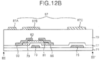
- FIG. 7 is a plan view showing an exemplary array substrate of a liquid crystal display according to the present invention
- FIG. 8 is a cross sectional view of the array substrate taken along III–III′ in FIG. 7 .
- a lower substrate 71 of an LCD may include a TFT arranged at an intersection between a gate line 75 and a data line 93 , a pixel electrode 91 connected to a drain electrode 85 of the TFT, and a storage capacitor to overlap with a partial area of the gate line 75 and the data line 93 .
- the TFT may include a gate electrode 73 connected to the gate line 75 , a source electrode 83 connected to the data line 93 , and a drain electrode 85 connected, via a contact hole 90 a , to the pixel electrode 91 . Furthermore, the TFT may include a gate insulating film 77 insulating the gate electrode 73 , and the source and drain electrodes 83 and 85 , and semiconductor layers 79 and 81 defining a conduction channel between the source electrode 83 and the drain electrode 85 by application of a gate voltage to the gate electrode 73 . Accordingly, the TFT responds to a gate signal from the gate line 75 to selectively apply a data signal from the data line 93 to the pixel electrode 91 .
- the pixel electrode 91 may be positioned on an upper insulating layer 89 at a cell area divided by the data line 93 and the gate line 75 , and may be made from a transparent conductive material having a high light transmittance, for example.
- the pixel electrode 91 may use an organic protective film 79 having a small dielectric constant formed such that a portion overlaps the data line 93 . Accordingly, the pixel electrode 91 may have an increased aperture ratio as compared to a pixel electrode that uses an inorganic protective film.
- the pixel electrode 91 may be electrically connected, via the contact hole 90 a defined at the organic protective film 79 and the upper insulating film 89 , to the drain electrode 85 .
- the pixel electrode 91 generates a potential difference from a common transparent electrode (not shown) provided at an upper substrate (not shown) by a data signal applied via the TFT.
- the potential difference allows a liquid crystal positioned between the lower substrate 71 and the upper substrate (not shown) to change a liquid crystal molecule arrangement owing to its dielectric anisotropy characteristic. Accordingly, an arrangement of liquid crystal molecules is changed for each pixel in accordance with a data voltage applied via the TFT, thereby expressing image data (picture information) on the LCD.
- the storage capacitor may include a pixel electrode 91 electrically connected, via the contact hole 90 a , to the drain electrode 85 , and a capacitor common line 75 having the upper insulating film 89 disposed therebetween.
- the capacitor common line 87 may overlap the gate line 75 , and a portion of the data line 93 to create a relatively large electrode area, thereby increasing a capacitance value of the storage capacitor.
- the capacitor common line 87 may overlap the gate line 75 , and the data line 93 so as not to occupy additional area, thereby increasing an aperture ratio.
- the capacitor common line 75 may extend to be commonly connected to the common line 75 and apply a similar common voltage as the common electrode (not shown) of the upper substrate (not shown). Also, the capacitor common line 87 may serve as a black matrix for extinguishing light along the gate line 75 and the data line 93 , whereby formation of an additional black matrix on the upper substrate is unnecessary.
- FIGS. 9 to 14 are cross sectional views of an exemplary method of fabricating the array substrate of the LCD shown in FIG. 8 according to the present invention.
- a gate electrode 73 , and a gate line 75 may be provided on a substrate 71 .
- the gate electrode 73 and the gate line 75 may be formed by depositing aluminum (Al) or copper (Cu) material, for example, using a deposition technique such as a sputtering, for example, and patterning the material.
- a gate insulating film 77 may be provided on the substrate 71 .
- the gate insulating film 77 may be formed by depositing an insulating material such as silicon nitride (SiN x ) or silicon oxide (SiO x ), for example, onto the substrate 71 using a plasma enhanced chemical vapor deposition (PECVD) technique, for example, to cover the gate electrode 73 and the gate line 75 .
- PECVD plasma enhanced chemical vapor deposition
- the active layer 79 and the ohmic contact layer 81 may be formed by sequentially depositing two semiconductor layers on the gate insulating film 77 and patterning the deposited semiconductor layers.
- the active layer 79 may be formed from amorphous silicon that is not doped with an impurity, for example, and the ohmic contact layer 81 may be formed from amorphous silicon doped with an n-type or p-type impurity at a high concentration, for example.
- a data line 93 , and source and drain electrodes 83 and 85 may be provided on the substrate 71 .
- the data line 93 , and the source and drain electrodes 83 and 85 may be formed by depositing a metal layer using CVD or sputtering techniques, for example, and patterning the metal layer. After the source and drain electrodes 83 and 85 are formed, the ohmic contact layer 81 at an area corresponding to the gate electrode 73 may be patterned to expose the active layer 79 , thereby creating a channel within an area of the active layer 79 corresponding to the gate electrode 73 between the source and drain electrodes 83 and 85 .
- the data line 93 , and the source and drain electrodes 83 and 85 may include chrome (Cr) or molybdenum (Mo) material, for example.
- an organic protective film 79 and a capacitor common line 87 may be sequentially provided on the substrate 71 .
- the organic protective film 79 may be formed by coating an insulating material on the gate insulating layer 77 using a spin coating technique to cover the source and drain electrodes 83 and 85 , for example. Accordingly, a surface of the organic protective film 79 may be flattened.
- the capacitor common line 87 may be provided to overlap the gate line 75 and a portion of the data line 93 by depositing a conductive material on the organic protective film 79 , for example, and patterning the material.
- the capacitor common line 87 may include a body 87 C overlapping end portions of the pixel electrode 91 , and the gate line 75 , and two arms 87 A and 87 B connected to the body 87 C and overlapping opposing sides of the data line 93 .
- the body 87 C of the capacitor common line 87 may be set to have a width larger than widths of each of the arms 87 A and 87 B.
- the organic protective film 79 may be formed from an organic insulating material having a small dielectric constant such as Teflon7, benzocyclobutene (BCB), Cytop7 or perfluorocyclobutane (PFCB), for example.
- a dielectric constant of the organic protective film 79 is between about 2 and about 4.
- a thickness of the organic protective film 79 is preferably between about 1 ⁇ m and about 3 ⁇ m to sufficiently reduce a parasitic capacitance formed at the overlapping portions between the capacitor common line 87 and the gate line 75 .
- an upper insulating layer 89 may be provided on the organic protective film 79 .
- the upper insulating layer 89 may be formed by depositing an insulating material on the organic protective film 79 using a plasma enhanced chemical vapor deposition (PECVD) technique, for example, to cover the capacitor common line 87 . Subsequently, the upper insulating layer 89 and the organic protective film 79 may be patterned to form the contact hole 90 a to expose the drain electrode 85 .
- the upper insulating layer 89 may include an inorganic insulating material such as silicon nitride (SiN x ) or silicon oxide (SiO x ), for example.
- a pixel electrode 91 may be provided on the upper insulating layer 89 .
- the pixel electrode 91 may be formed by depositing a transparent conductive material on the upper insulating layer 89 , and patterning the material, for example.
- the pixel electrode 91 may be electrically connected, via the contact hole 90 a , to the drain electrode 85 , and may include any one of ITO, IZO and ITZO, for example.
- FIG. 15 is a plan view showing another exemplary array substrate of a liquid crystal display according to the present invention
- FIG. 16 is a cross sectional view of the array substrate taken along IV–IV′ in FIG. 15 according to the present invention.
- a lower substrate 101 of a LCD may include a TFT arranged at an intersection between a gate line 105 and a data line 117 , a pixel electrode 125 connected to a drain electrode 115 of the TFT, and a storage capacitor positioned at an overlapping portion between the gate line 105 and a part of the data line 117 .
- the TFT may include a gate electrode 103 protruding from the gate line 105 , a source electrode 113 protruding from the data line 117 , and a drain electrode 115 connected, via a first contact hole 120 a , to the pixel electrode 125 . Furthermore, the TFT may include a gate insulating film 107 insulating the gate electrode 113 and the source and drain electrodes 113 and 115 , and semiconductor layers 109 and 111 defining a conduction channel between the source electrode 113 and the drain electrode 115 by application of a gate voltage to the gate electrode 103 . Accordingly, the TFT responds to a gate signal from the gate line 105 to selectively apply a data signal from the data line 117 to the pixel electrode 125 .
- the pixel electrode 125 may be positioned on an upper insulating layer 123 coated on an entire surface of the lower substrate 101 at a cell area divided by the data line 93 and the gate line 75 .
- the pixel electrode may include a transparent conductive material having a high light transmittance, for example.
- the pixel electrode 125 may use an organic protective film 118 having a small dielectric constant such that a portion overlaps the data line 117 . Accordingly, the pixel electrode may have an increased aperture ratio as compared to a pixel electrode that uses an inorganic protective film.
- the pixel electrode 125 may be electrically connected, via the first contact hole 120 a defined by the upper insulating layer 123 and the organic protective film 118 , to the drain electrode 115 .
- the storage capacitor should have a large capacitance to maintain a stable pixel voltage.
- the storage capacitor may include a parallel connection of a first storage capacitor of a storage-on-common system, and a second storage capacitor of a storage-on-gate system.
- the first storage capacitor may include the pixel electrode 125 , and a capacitor common line 121 having an upper insulating layer 123 disposed therebetween with the capacitor common line 121 overlapping the gate line 105 and a portion of the data line 117 .
- the capacitor common line 121 may serve as a black matrix for extinguishing light along the gate line 105 and the data line 117 , whereby formation of an additional black matrix on the upper substrate is unnecessary.
- the second storage capacitor may include a capacitor electrode 119 connected, via a second contact hole 120 b , to the pixel electrode 119 , and the gate line having the gate insulating film 107 disposed therebetween.
- a capacitance value of the storage capacitor is increased by a combination of the first and second storage capacitors.
- the capacitor common line 121 and the capacitor electrode 119 overlap with the gate line 105 and the data line 117 so as not to occupy additional area, thereby increasing an aperture ratio.
- FIGS. 17 to 22 are cross sectional views of another exemplary method of fabricating the array substrate of the LCD shown in FIG. 16 according to the present invention.
- a gate electrode 103 and a gate line 105 may be provided on a substrate 101 .
- the gate electrode 103 and the gate line 105 may be formed by depositing aluminum (Al) or copper (Cu) material, for example, using a deposition technique such as a sputtering, for example, and patterning the material.
- a gate insulating film 107 , an active layer 109 and an ohmic contact layer 111 may be provided on the substrate 101 .
- the gate insulating film 107 may be formed by depositing an insulating material such as silicon nitride (SiN x ) or silicon oxide (SiO x ), for example, onto the substrate 101 using a plasma enhanced chemical vapor deposition (PECVD) technique, for example, to cover the gate electrode 103 and the gate line 105 .
- PECVD plasma enhanced chemical vapor deposition
- the active layer 109 and the ohmic contact layer 111 may be formed by sequentially depositing two semiconductor layers on the gate insulating film 107 and patterning the deposited semiconductor layers.
- the active layer 109 may be formed from amorphous silicon that is not doped with an impurity, for example, and the ohmic contact layer 111 may be formed from amorphous silicon doped with an n-type or p-type impurity at a high concentration, for example.
- a data line 117 , source and drain electrodes 113 and 115 , and a capacitor electrode 119 may be provided on the substrate 101 .
- the data line 117 , the source and drain electrodes 113 and 115 , and the capacitor electrode 119 may be formed by depositing a metal layer using CVD or sputtering techniques, for example, and patterning the metal layer.
- the data line 117 , the source and drain electrodes 113 and 115 , and the capacitor electrode 119 may include chrome (Cr) or molybdenum (Mo) material, for example.
- a portion of the ohmic contact layer 111 at an area corresponding to the gate electrode 103 may be patterned to expose the active layer 109 , thereby creating a channel within an area of the active layer 109 corresponding to the gate electrode 103 between the source and drain electrodes 113 and 115 .
- an organic protective film 118 and a capacitor common line 121 may be sequentially provided on the substrate 101 .
- the organic protective film 118 may be formed by coating an insulating material on the gate insulating layer 107 using a spin coating technique, for example, to cover the source and drain electrodes 113 and 115 . Accordingly, a surface of the organic protective film 118 may be flattened.
- the capacitor common line 121 may be provided to overlap the gate line 105 and a portion of the data line 117 by depositing a transparent conductive material onto the organic protective film 118 , for example, and patterning the material.
- the capacitor common line 121 may include a body 121 C overlapping upper end portions of the pixel electrode 125 and the gate line 105 , and two arms 121 A and 121 B connected to the body 121 C and overlapping opposing sides of the data line 121 .
- the body 121 C of the capacitor common line 121 may be set to have a width larger than each of the arms 121 A and 121 B.
- a hole 121 D may be defined at a portion where a contact hole is to be formed during post-processing in the body 121 C of the capacitor common line 121 overlapping the storage capacitor 119 .
- the organic protective film 118 may be formed from an organic insulating material having a small dielectric constant such as Teflon7, benzocyclobutene (BCB), Cytop7 or perfluorocyclobutane (PFCB).
- a dielectric constant of the organic protective film 118 is between about 2 and about 4.
- a thickness of the organic protective film 118 is preferably between about 1 ⁇ m and about 3 ⁇ m to sufficiently reduce a parasitic capacitance formed at the overlapping portions between the capacitor common line 121 and the gate line 105 .
- an upper insulating layer 123 and first and second contact holes 120 a and 120 b may be provided in the organic protective film 118 .
- the upper insulating layer 123 may be formed by depositing an insulating material on the organic protective film 118 using a plasma enhanced chemical vapor deposition (PECVD) technique, for example, to cover the capacitor common line 121 . Subsequently, the upper insulating layer 123 and the organic protective film 118 may be simultaneously patterned to form the first and second contact holes 120 a and 120 b to expose the drain electrode 115 , and the capacitor electrode 119 , respectively.
- the upper insulating layer 123 may include an inorganic insulating material such as silicon nitride (SiN x ) or silicon oxide (SiO x ), for example.
- a pixel electrode 125 may be provided on the upper insulating layer 125 .
- the pixel electrode 125 may be formed by depositing a transparent conductive material on the upper insulating layer 123 , and patterning the material, for example.
- the pixel electrode 125 may be electrically connected, via the first contact hole 120 a , to the drain electrode 115 , and may include.
- the pixel electrode 125 may electrically contact the capacitor electrode 119 through the second contact hole 120 b .
- the pixel electrode 125 may include any one of ITO, IZO and ITZO, for example.
Abstract
Description
Claims (9)
Priority Applications (1)
| Application Number | Priority Date | Filing Date | Title |
|---|---|---|---|
| US11/528,591 US7425997B2 (en) | 2001-06-05 | 2006-09-28 | Array substrate of liquid crystal display and fabricating method thereof |
Applications Claiming Priority (2)
| Application Number | Priority Date | Filing Date | Title |
|---|---|---|---|
| KRP2001-31511 | 2001-06-05 | ||
| KR1020010031511A KR100620847B1 (en) | 2001-06-05 | 2001-06-05 | Array Substrate of Liquid Crystal Display and Fabricating Method Thereof |
Related Child Applications (1)
| Application Number | Title | Priority Date | Filing Date |
|---|---|---|---|
| US11/528,591 Division US7425997B2 (en) | 2001-06-05 | 2006-09-28 | Array substrate of liquid crystal display and fabricating method thereof |
Publications (2)
| Publication Number | Publication Date |
|---|---|
| US20020180901A1 US20020180901A1 (en) | 2002-12-05 |
| US7133087B2 true US7133087B2 (en) | 2006-11-07 |
Family
ID=19710425
Family Applications (2)
| Application Number | Title | Priority Date | Filing Date |
|---|---|---|---|
| US10/141,848 Expired - Lifetime US7133087B2 (en) | 2001-06-05 | 2002-05-10 | Array substrate of liquid crystal display and fabricating method thereof |
| US11/528,591 Expired - Lifetime US7425997B2 (en) | 2001-06-05 | 2006-09-28 | Array substrate of liquid crystal display and fabricating method thereof |
Family Applications After (1)
| Application Number | Title | Priority Date | Filing Date |
|---|---|---|---|
| US11/528,591 Expired - Lifetime US7425997B2 (en) | 2001-06-05 | 2006-09-28 | Array substrate of liquid crystal display and fabricating method thereof |
Country Status (2)
| Country | Link |
|---|---|
| US (2) | US7133087B2 (en) |
| KR (1) | KR100620847B1 (en) |
Cited By (7)
| Publication number | Priority date | Publication date | Assignee | Title |
|---|---|---|---|---|
| US20060221031A1 (en) * | 2005-04-01 | 2006-10-05 | Hak-Sun Chang | Display panel and display device having the same |
| US20060256246A1 (en) * | 2005-05-11 | 2006-11-16 | Ming-Zen Wu | Thin film transistor array |
| US20070058096A1 (en) * | 2005-09-12 | 2007-03-15 | Wintek Corporation | Storage capacitor structure for liquid crystal display |
| US20070158729A1 (en) * | 2005-12-29 | 2007-07-12 | Young-Chol Yang | Thin film transistor array panel and method of manufacture |
| US20090141222A1 (en) * | 2007-11-30 | 2009-06-04 | Shih-Chia Hsu | Transflective licuid crystal display panel and pixel structure thereof |
| US20100134454A1 (en) * | 2002-03-04 | 2010-06-03 | Hitachi, Ltd. | Organic electroluminescent light emitting display device |
| US7982833B2 (en) | 2007-10-19 | 2011-07-19 | Au Optronics Corp. | Transflective liquid crystal display panel having a plurality of apertures with a specific ratio of aperture width to aperture interval |
Families Citing this family (43)
| Publication number | Priority date | Publication date | Assignee | Title |
|---|---|---|---|---|
| KR100835974B1 (en) * | 2001-12-24 | 2008-06-09 | 엘지디스플레이 주식회사 | An array substrate for In-Plane switching mode LCD and method for fabricating the same |
| TW574540B (en) * | 2002-09-13 | 2004-02-01 | Toppoly Optoelectronics Corp | Pixel structure of TFT LCD |
| KR101157222B1 (en) * | 2003-06-28 | 2012-06-15 | 엘지디스플레이 주식회사 | Liquid crystal display panel of horizontal electronic field applying type and fabricating method thereof |
| JP4381063B2 (en) * | 2003-08-18 | 2009-12-09 | 東芝モバイルディスプレイ株式会社 | Array substrate and flat display device |
| KR101006436B1 (en) * | 2003-11-18 | 2011-01-06 | 삼성전자주식회사 | Thin film transistor array panel for display device |
| KR20050060963A (en) * | 2003-12-17 | 2005-06-22 | 엘지.필립스 엘시디 주식회사 | Thin film transistor array substrate and fabricating method thereof |
| KR20060046241A (en) * | 2004-06-29 | 2006-05-17 | 엘지.필립스 엘시디 주식회사 | Liquid crystal display device |
| CN100476554C (en) * | 2004-08-31 | 2009-04-08 | 卡西欧计算机株式会社 | Vertical alignment active matrix liquid crystal display device |
| JP4275038B2 (en) * | 2004-09-01 | 2009-06-10 | シャープ株式会社 | Active matrix substrate and display device including the same |
| CN100492141C (en) * | 2004-09-30 | 2009-05-27 | 卡西欧计算机株式会社 | Vertical alignment active matrix liquid crystal display device |
| US20060066791A1 (en) * | 2004-09-30 | 2006-03-30 | Casio Computer Co., Ltd. | Vertical alignment active matrix liquid crystal display device |
| TWI290649B (en) * | 2004-11-29 | 2007-12-01 | Casio Computer Co Ltd | Vertical alignment active matrix liquid crystal display device |
| KR100752876B1 (en) * | 2004-11-30 | 2007-08-29 | 가시오게산키 가부시키가이샤 | Vertical-alignment liquid crystal display device |
| KR101112544B1 (en) * | 2004-12-03 | 2012-03-13 | 삼성전자주식회사 | Thin film transistor array panel and method for manufacturing the same |
| JP4484881B2 (en) * | 2004-12-16 | 2010-06-16 | シャープ株式会社 | Active matrix substrate, display device, liquid crystal display device, and television device |
| JP4639797B2 (en) * | 2004-12-24 | 2011-02-23 | カシオ計算機株式会社 | Liquid crystal display element |
| US8068200B2 (en) | 2004-12-24 | 2011-11-29 | Casio Computer Co., Ltd. | Vertical alignment liquid crystal display device in which a pixel electrode has slits which divide the pixel electrode into electrode portions |
| KR101232618B1 (en) * | 2005-01-17 | 2013-02-13 | 삼성디스플레이 주식회사 | Array substrate, and liquid crystal display panel and liquid crystal display device having the same |
| US7573537B2 (en) * | 2005-01-17 | 2009-08-11 | Samsung Electronics Co., Ltd. | Array substrate, liquid crystal display panel having the same and liquid crystal display device having the same |
| US8049699B2 (en) * | 2005-02-07 | 2011-11-01 | Samsung Electronics Co., Ltd. | Liquid crystal display apparatus having storage electrodes overlapping only some sub-pixels |
| KR101187207B1 (en) * | 2005-08-04 | 2012-10-02 | 삼성디스플레이 주식회사 | Liquid crystal display |
| KR101219046B1 (en) * | 2005-11-17 | 2013-01-08 | 삼성디스플레이 주식회사 | Display device and manufacturing method thereof |
| US7688392B2 (en) * | 2006-04-06 | 2010-03-30 | Chunghwa Picture Tubes, Ltd. | Pixel structure including a gate having an opening and an extension line between the data line and the source |
| KR101310284B1 (en) | 2006-09-28 | 2013-09-24 | 삼성디스플레이 주식회사 | Display device, display substrate and method for manufacturing the display substrate |
| CN201041604Y (en) * | 2006-11-24 | 2008-03-26 | 群康科技(深圳)有限公司 | Liquid crystal display device |
| CN103488012B (en) * | 2012-06-08 | 2016-02-17 | 瀚宇彩晶股份有限公司 | The method for making of dot structure, dot structure and active elements array substrates |
| TWI473057B (en) * | 2013-01-30 | 2015-02-11 | Au Optronics Corp | Pixel unit and pixel array |
| JP2015014640A (en) * | 2013-07-03 | 2015-01-22 | 株式会社ジャパンディスプレイ | Liquid crystal display device |
| CN103499905A (en) * | 2013-10-17 | 2014-01-08 | 北京京东方光电科技有限公司 | Array substrate, manufacturing method thereof and display device |
| CN103558719A (en) * | 2013-11-12 | 2014-02-05 | 深圳市华星光电技术有限公司 | Pixel structure and manufacturing method thereof |
| TWI518430B (en) * | 2013-12-02 | 2016-01-21 | 群創光電股份有限公司 | Display panel and display device using the same |
| CN103984161B (en) * | 2013-12-30 | 2017-08-25 | 厦门天马微电子有限公司 | Array base palte and its manufacture method, liquid crystal display panel and liquid crystal display device |
| CN103928400A (en) * | 2014-03-31 | 2014-07-16 | 京东方科技集团股份有限公司 | Array substrate, manufacturing method thereof and display device |
| CN104183604A (en) * | 2014-08-04 | 2014-12-03 | 深圳市华星光电技术有限公司 | TET-LCD array substrate and manufacture method thereof |
| CN104678671B (en) * | 2015-03-30 | 2018-12-21 | 京东方科技集团股份有限公司 | Display base plate and its manufacturing method and display device |
| TWI567462B (en) * | 2015-09-09 | 2017-01-21 | 友達光電股份有限公司 | Pixel structure and pixel array |
| CN105116642B (en) | 2015-09-24 | 2018-07-17 | 京东方科技集团股份有限公司 | Array substrate and preparation method thereof, display device |
| CN105629605B (en) * | 2016-01-06 | 2019-01-22 | 深圳市华星光电技术有限公司 | Array substrate, liquid crystal display panel and liquid crystal display device |
| TWI649603B (en) * | 2016-04-27 | 2019-02-01 | 友達光電股份有限公司 | Pixel structure, display panel and curved display device |
| KR102620013B1 (en) * | 2016-07-01 | 2024-01-02 | 삼성디스플레이 주식회사 | Organic lihgt emitting display device and manufacturing method of the same |
| CN107153308B (en) * | 2017-06-19 | 2020-08-28 | 深圳市华星光电技术有限公司 | Array substrate and manufacturing method |
| CN107544183B (en) * | 2017-09-20 | 2018-10-30 | 南京中电熊猫液晶显示科技有限公司 | A kind of liquid crystal display device |
| CN111965908B (en) * | 2020-08-27 | 2023-10-24 | 京东方科技集团股份有限公司 | Array substrate and display device |
Citations (7)
| Publication number | Priority date | Publication date | Assignee | Title |
|---|---|---|---|---|
| KR940011988A (en) | 1992-11-20 | 1994-06-22 | 이헌조 | LCD Display |
| US5905548A (en) * | 1997-02-25 | 1999-05-18 | Sharp Kabushiki Kaisha | Liquid crystal display device with large aperture ratio |
| KR20000002804A (en) | 1998-06-23 | 2000-01-15 | 김영환 | Liquid crystal display device |
| JP2001066633A (en) | 1999-08-26 | 2001-03-16 | Sharp Corp | Liquid crystal display device and projection liquid crystal display device |
| KR20010026625A (en) | 1999-09-08 | 2001-04-06 | 구본준 | Liquid crystal display and method for fabricating the same |
| US6466281B1 (en) * | 1999-08-23 | 2002-10-15 | Industrial Technology Research Institute | Integrated black matrix/color filter structure for TFT-LCD |
| US6610997B2 (en) * | 2000-03-17 | 2003-08-26 | Seiko Epson Corporation | Electro-optical device |
Family Cites Families (8)
| Publication number | Priority date | Publication date | Assignee | Title |
|---|---|---|---|---|
| US6372534B1 (en) * | 1995-06-06 | 2002-04-16 | Lg. Philips Lcd Co., Ltd | Method of making a TFT array with photo-imageable insulating layer over address lines |
| JP3634089B2 (en) * | 1996-09-04 | 2005-03-30 | 株式会社半導体エネルギー研究所 | Display device |
| JP3291249B2 (en) * | 1998-07-16 | 2002-06-10 | アルプス電気株式会社 | Active matrix type liquid crystal display device and substrate used therefor |
| KR100474003B1 (en) * | 1998-11-27 | 2005-09-16 | 엘지.필립스 엘시디 주식회사 | Liquid crystal display device |
| US6614083B1 (en) * | 1999-03-17 | 2003-09-02 | Semiconductor Energy Laboratory Co., Ltd. | Wiring material and a semiconductor device having wiring using the material, and the manufacturing method |
| JP3916823B2 (en) * | 1999-04-07 | 2007-05-23 | シャープ株式会社 | Active matrix substrate, manufacturing method thereof, and flat panel image sensor |
| US6654073B1 (en) * | 1999-09-01 | 2003-11-25 | Nec Lcd Technologies, Ltd. | Liquid crystal display having storage capacitance electrodes and method of fabricating the same |
| KR100560777B1 (en) * | 2001-03-26 | 2006-03-13 | 삼성에스디아이 주식회사 | A TFT pixel for driving an electroluminescent display device |
-
2001
- 2001-06-05 KR KR1020010031511A patent/KR100620847B1/en active IP Right Grant
-
2002
- 2002-05-10 US US10/141,848 patent/US7133087B2/en not_active Expired - Lifetime
-
2006
- 2006-09-28 US US11/528,591 patent/US7425997B2/en not_active Expired - Lifetime
Patent Citations (7)
| Publication number | Priority date | Publication date | Assignee | Title |
|---|---|---|---|---|
| KR940011988A (en) | 1992-11-20 | 1994-06-22 | 이헌조 | LCD Display |
| US5905548A (en) * | 1997-02-25 | 1999-05-18 | Sharp Kabushiki Kaisha | Liquid crystal display device with large aperture ratio |
| KR20000002804A (en) | 1998-06-23 | 2000-01-15 | 김영환 | Liquid crystal display device |
| US6466281B1 (en) * | 1999-08-23 | 2002-10-15 | Industrial Technology Research Institute | Integrated black matrix/color filter structure for TFT-LCD |
| JP2001066633A (en) | 1999-08-26 | 2001-03-16 | Sharp Corp | Liquid crystal display device and projection liquid crystal display device |
| KR20010026625A (en) | 1999-09-08 | 2001-04-06 | 구본준 | Liquid crystal display and method for fabricating the same |
| US6610997B2 (en) * | 2000-03-17 | 2003-08-26 | Seiko Epson Corporation | Electro-optical device |
Cited By (13)
| Publication number | Priority date | Publication date | Assignee | Title |
|---|---|---|---|---|
| US8134524B2 (en) * | 2002-03-04 | 2012-03-13 | Hitachi Displays, Ltd. | Organic electroluminescent light emitting display device |
| US20100134454A1 (en) * | 2002-03-04 | 2010-06-03 | Hitachi, Ltd. | Organic electroluminescent light emitting display device |
| US8446347B2 (en) | 2002-03-04 | 2013-05-21 | Hitachi Displays, Ltd. | Organic electroluminescent light emitting display device |
| US8847858B2 (en) | 2002-03-04 | 2014-09-30 | Japan Display Inc. | Organic electroluminescent light emitting display device |
| US11289565B2 (en) | 2002-03-04 | 2022-03-29 | Samsung Display Co., Ltd. | Organic electroluminescent light emitting display device |
| US20060221031A1 (en) * | 2005-04-01 | 2006-10-05 | Hak-Sun Chang | Display panel and display device having the same |
| US20060256246A1 (en) * | 2005-05-11 | 2006-11-16 | Ming-Zen Wu | Thin film transistor array |
| US7557872B2 (en) * | 2005-05-11 | 2009-07-07 | Chunghwa Picture Tubes, Ltd. | Thin film transistor array |
| US20070058096A1 (en) * | 2005-09-12 | 2007-03-15 | Wintek Corporation | Storage capacitor structure for liquid crystal display |
| US20070158729A1 (en) * | 2005-12-29 | 2007-07-12 | Young-Chol Yang | Thin film transistor array panel and method of manufacture |
| US7982833B2 (en) | 2007-10-19 | 2011-07-19 | Au Optronics Corp. | Transflective liquid crystal display panel having a plurality of apertures with a specific ratio of aperture width to aperture interval |
| US20090141222A1 (en) * | 2007-11-30 | 2009-06-04 | Shih-Chia Hsu | Transflective licuid crystal display panel and pixel structure thereof |
| US7751002B2 (en) | 2007-11-30 | 2010-07-06 | Au Optronics Corp. | Transflective LCD panel and pixel structure with first and second overlapping common electrodes disposed in one direction both overlapping data line disposed in a second direction |
Also Published As
| Publication number | Publication date |
|---|---|
| KR100620847B1 (en) | 2006-09-13 |
| US20070019124A1 (en) | 2007-01-25 |
| US7425997B2 (en) | 2008-09-16 |
| KR20020092720A (en) | 2002-12-12 |
| US20020180901A1 (en) | 2002-12-05 |
Similar Documents
| Publication | Publication Date | Title |
|---|---|---|
| US7133087B2 (en) | Array substrate of liquid crystal display and fabricating method thereof | |
| US6788357B2 (en) | Array substrate for a liquid crystal display and method for fabricating thereof | |
| KR101183361B1 (en) | Array substrate for LCD and the fabrication method thereof | |
| US7333161B2 (en) | Forming method of liquid crystal layer using ink jet system | |
| US7301597B2 (en) | Array substrate for a liquid crystal display device and manufacturing method of the same | |
| US7916229B2 (en) | Liquid crystal display device and method for fabricating the same | |
| US7212255B2 (en) | Liquid crystal display device and fabricating method thereof | |
| US7170571B2 (en) | Liquid crystal display device with double metal layer source and drain electrodes and fabricating method thereof | |
| KR101213871B1 (en) | Thin film transistor array substrate and manufacturing method of the same | |
| US7230658B2 (en) | Array substrate with driving TFT and synchronization adjustment TFT | |
| KR20030004871A (en) | Array Substrate of Liquid Crystal Display and Fabricating Method Thereof | |
| JP2001013520A (en) | Active matrix type liquid crystal display device | |
| US20120161140A1 (en) | Tft array substrate and manufacturing method thereof | |
| US20070285591A1 (en) | Liquid crystal display panel and method of manufacturing the same | |
| KR100797374B1 (en) | Liquid Crystal Display and Fabricating Method Thereof | |
| US8378944B2 (en) | Array substrate for in-plane switching mode liquid crystal display device | |
| US6724453B2 (en) | Method of fabricating array substrate for use in an in-plane switching mode liquid crystal display device | |
| US6791651B2 (en) | Array substrate for IPS mode liquid crystal display device and fabricating method for the same | |
| KR20050001936A (en) | Thin film transistor and manufacturing method thereof and thin film transistor array substrate and manufacturing method thereof using the same | |
| US6411347B1 (en) | Storage capacitor in a liquid crystal display and a method of manufacturing thereof | |
| US20020047948A1 (en) | Array substrate for a liquid crystal display and method for fabricating thereof | |
| US20070153143A1 (en) | Array substrate for liquid crystal display and manufacturing method thereof | |
| KR100453162B1 (en) | Liquid Crystal Display Device and Fabricating Method Thereof | |
| KR101142981B1 (en) | Thin film transistor array substrate and manufacturing method of the same | |
| KR20010068334A (en) | Liquid Crystal Display Device and Fabricating Method Thereof |
Legal Events
| Date | Code | Title | Description |
|---|---|---|---|
| AS | Assignment |
Owner name: LG. PHILIPS LCD CO., LTD., KOREA, REPUBLIC OF Free format text: ASSIGNMENT OF ASSIGNORS INTEREST;ASSIGNOR:KIM, WOO HYUN;REEL/FRAME:012895/0218 Effective date: 20020502 |
|
| STCF | Information on status: patent grant |
Free format text: PATENTED CASE |
|
| FEPP | Fee payment procedure |
Free format text: PAYER NUMBER DE-ASSIGNED (ORIGINAL EVENT CODE: RMPN); ENTITY STATUS OF PATENT OWNER: LARGE ENTITY Free format text: PAYOR NUMBER ASSIGNED (ORIGINAL EVENT CODE: ASPN); ENTITY STATUS OF PATENT OWNER: LARGE ENTITY |
|
| AS | Assignment |
Owner name: LG DISPLAY CO., LTD., KOREA, REPUBLIC OF Free format text: CHANGE OF NAME;ASSIGNOR:LG.PHILIPS LCD CO., LTD.;REEL/FRAME:021147/0009 Effective date: 20080319 Owner name: LG DISPLAY CO., LTD.,KOREA, REPUBLIC OF Free format text: CHANGE OF NAME;ASSIGNOR:LG.PHILIPS LCD CO., LTD.;REEL/FRAME:021147/0009 Effective date: 20080319 |
|
| FEPP | Fee payment procedure |
Free format text: PAYER NUMBER DE-ASSIGNED (ORIGINAL EVENT CODE: RMPN); ENTITY STATUS OF PATENT OWNER: LARGE ENTITY Free format text: PAYOR NUMBER ASSIGNED (ORIGINAL EVENT CODE: ASPN); ENTITY STATUS OF PATENT OWNER: LARGE ENTITY |
|
| FPAY | Fee payment |
Year of fee payment: 4 |
|
| FPAY | Fee payment |
Year of fee payment: 8 |
|
| MAFP | Maintenance fee payment |
Free format text: PAYMENT OF MAINTENANCE FEE, 12TH YEAR, LARGE ENTITY (ORIGINAL EVENT CODE: M1553) Year of fee payment: 12 |