US7155195B2 - Input and output filtering system for a direct conversion receiver - Google Patents
Input and output filtering system for a direct conversion receiver Download PDFInfo
- Publication number
- US7155195B2 US7155195B2 US10/172,239 US17223902A US7155195B2 US 7155195 B2 US7155195 B2 US 7155195B2 US 17223902 A US17223902 A US 17223902A US 7155195 B2 US7155195 B2 US 7155195B2
- Authority
- US
- United States
- Prior art keywords
- filter
- signals
- signal
- frequency range
- frequency
- Prior art date
- Legal status (The legal status is an assumption and is not a legal conclusion. Google has not performed a legal analysis and makes no representation as to the accuracy of the status listed.)
- Expired - Lifetime, expires
Links
Images


Classifications
-
- H—ELECTRICITY
- H04—ELECTRIC COMMUNICATION TECHNIQUE
- H04B—TRANSMISSION
- H04B1/00—Details of transmission systems, not covered by a single one of groups H04B3/00 - H04B13/00; Details of transmission systems not characterised by the medium used for transmission
- H04B1/06—Receivers
- H04B1/10—Means associated with receiver for limiting or suppressing noise or interference
- H04B1/12—Neutralising, balancing, or compensation arrangements
-
- H—ELECTRICITY
- H04—ELECTRIC COMMUNICATION TECHNIQUE
- H04B—TRANSMISSION
- H04B1/00—Details of transmission systems, not covered by a single one of groups H04B3/00 - H04B13/00; Details of transmission systems not characterised by the medium used for transmission
- H04B1/06—Receivers
- H04B1/16—Circuits
- H04B1/30—Circuits for homodyne or synchrodyne receivers
Definitions
- the present invention is generally related to receivers and, more particularly to a system and method for filtering the baseband signal in a receiver.
- Wireless technology has undergone vast improvements in the last several years, both in terms of communication theory and hardware design. Improved hardware has sped the development of digital communications, and the digital nature of the communications link has allowed engineers to transfer larger amounts of data across a wireless link. Moreover, the improvements in hardware have allowed transmitters and receivers to operate at higher and higher frequencies, thus making even higher data rates possible.
- the receiver receives the high frequency radio signal and converts it down to baseband through at least one intermediate frequency (IF).
- IF intermediate frequency
- the receiver filters out a majority of the noise from the adjacent channels (both upper and lower).
- the filtering is done at intermediate frequencies because high frequency filters are expensive and generally difficult to realize because the bandwidth, as the percentage of the center frequency, is very low.
- lowering the high frequency signal to an intermediate frequency allows the designer to use realizable filters.
- these filters take the form of intermediate frequency surface acoustic wave (IF SAW) filters.
- IF SAW intermediate frequency surface acoustic wave
- the direct conversion receiver directly converts the received high frequency radio signal to a baseband signal, rather than converting through one or more intermediate frequency steps.
- the IF SAW filters are not required. This saves a substantial amount of cost and reduces the size of the receiver.
- the channel filtering is achieved by using active low pass filters. These active low pass filters can be integrated on a chip along with the other receiver elements, thus reducing cost and size.
- the active filters are quite noisy.
- these active low pass filters have a limited dynamic range. Dynamic range is defined as the difference between the noise floor of the filter and the maximum signal level of an adjacent channel that can be tolerated.
- the dynamic range requirement of the active filters determines important design parameters such as the size and current consumption of these components. A larger size chip typically equates to higher cost, and minimizing current consumption in battery powered portable units is very important in prolonging battery life.
- direct conversion receivers are a conceptually simpler solution to the high frequency radio receiver, in practice direct conversion receivers can be more difficult to efficiently implement.
- An embodiment of the invention comprises a direct conversion receiver configured to enhance reception of a receive signal band.
- the invention comprises a plurality of receive signals comprising a receive band, and a first and second filter.
- the first filter is adapted to receive the plurality of receive signals, and is configured to attenuate a frequency range of the receive band to de-emphasize signals within the frequency range.
- the second filter is coupled to the output of a signal processing logic and configured to amplify the signals in the frequency range of the receive band, wherein the signal processing logic is coupled to the output of the first filter and is configured to substantially attenuate a plurality of unwanted signals in the receive band.
- Another embodiment of the invention comprises a filter configured to receive a receive band, the receive band being at a baseband frequency and comprising a plurality of signals.
- the filter is also configured to filter out a plurality of unwanted signals from the plurality of signals and configured to produce a desired signal, wherein the filter has a pole frequency that is located within a frequency range of the desired signal. The location of this pole frequency thereby enhances the attenuation of the plurality of unwanted signals prior to processing the desired signal in a direct conversion receiver signal processing logic.
- Another embodiment of the invention comprises a plurality of receive signals comprising a receive band and a flicker noise signal, a first filter and a second filter.
- the first filter is adapted to receive the receive band and configured to pass a plurality of low frequency signals substantially unaltered, while providing a constant attenuation value for a plurality of high frequency signals.
- the second filter is coupled to a signal processing logic output and configured to amplify the high frequency signals that were attenuated by the first filter to yield a desired signal.
- the signal processing logic being coupled to the output of the first filter and configured to attenuate the plurality of receive signals such that substantially only one signal remains.
- Another embodiment of the invention includes a method for enhancing reception on a direct conversion receiver. This method comprises attenuating a plurality of signals in a frequency range of a receive band, performing intermediate filtering on the receive band, amplifying the plurality of signals in the frequency range, and providing a desired baseband signal.
- Another embodiment of the invention includes a method comprising receiving a receive band, comprising a plurality of signals, and attenuating the receive band, such that a plurality of unwanted signals are rejected along with a portion of a desired signal, wherein a portion of the desired signal is allowed to pass.
- Another embodiment of the invention includes a method comprising receiving a receive band, the receive band comprising a plurality of signals, attenuating a frequency range of the plurality of signals, such that the frequency range is de-emphasized with respect to signals outside of the frequency range, providing signal processing to substantially remove a plurality of unwanted signals from the receive band, and amplifying the frequency range of the plurality of signals, such that the attenuated frequency range receives amplification substantially equal to the attenuation received in the attenuating step.
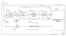
- FIG. 1 is a block diagram of a portion of radio receiver constructed in accordance with an embodiment of the present invention.
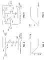
- FIG. 2 is a schematic diagram of one embodiment of the input filter of the present invention, as shown in FIG. 1 .
- FIG. 3 is a graph illustrating the transfer function of the input filter shown in FIG. 2 .
- FIG. 4 is a schematic diagram of one embodiment of the optional output filter as shown in FIG. 1 .
- FIG. 5 is a graph illustrating the transfer function of the output filter shown in FIG. 4 .
- FIG. 6 is a schematic diagram of an alternative embodiment of the input filter as shown in FIG. 1 .
- FIG. 7 is a graph illustrating the transfer function of the input filter shown in FIG. 6 .
- FIG. 8 is a schematic diagram of an alternative embodiment of the output filter as shown in FIG. 1 .
- FIG. 9 is a graph illustrating the transfer function of the output filter shown in FIG. 8 .
- FIG. 1 shows a simplified block diagram of a portion of a radio device 100 of which the direct conversion receiver 102 forms a part.
- This embodiment discusses the invention with regard to a low pass environment, wherein the receive signals have been converted to baseband prior to the filtering steps.
- teachings of the present invention can be adapted for use in a plurality of different environments, including environments where bandpass and even highpass filtering is called for.
- the antenna 104 receives a high frequency signal from another radio device and directs the signal to the receiver electronics of the radio device 100 .
- the high frequency signal is typically referred to as a “radio frequency” (RF) signal.
- Switch 106 is switched according to whether the receiver is transmitting or receiving a signal in this half-duplex radio.
- RF radio frequency
- a full-duplex radio could be utilized in accordance with the invention by replacing switch 106 with a diplexer.
- the diplexer as known to those skilled in the art, can be used to simultaneously pass transmit and receive signals to and from the antenna.
- a pre-selector filter 108 receives the RF signal and filters out all but the desired frequency band. Because filtering at high frequencies leads to expensive filters and higher power consumption, radios typically immediately convert the signal down to another frequency using a down-converter 110 , which can alternatively be a mixer or demodulator. In direct conversion receivers the signal from the pre-selector filter is down-converted to baseband. In contrast, the super-heterodyne architecture down-converts the receive signal to a frequency between baseband and the received frequency, before ultimately converting the receive signal to baseband.
- the desired frequency band becomes compressed.
- the desired frequency band typically comprises a plurality of data or voice signals, each occupying a different channel in the desired frequency band. Therefore, when the desired frequency band becomes compressed, each of the signals moves closer together. Therefore, filtering becomes more complex because the filters have to exhibit more selectivity in order to filter out the upper and lower adjacent unwanted signals from the desired signal. This increased complexity is the reason that super-heterodyne systems are often used in conjunction with high frequency communication standards.
- the super-heterodyne architecture which first converts the received RF signal to an intermediate frequency, generally uses a pair of intermediate frequency surface accoustic wave (IF SAW) filters to gain the selectivity required by most high frequency communication standards.
- IF SAW intermediate frequency surface accoustic wave
- the active IF SAW filters are expensive, and, moreover, active filters add significant noise to the signal.
- One way to reduce the expense and power consumption would be to find a method whereby the receiver could directly convert the signal to baseband, and then filter the signal in baseband while maintaining the required selectivity.
- Flicker noise can generally be described as a noise phenomenon which has a power spectrum that behaves according to the inverse of a signal frequency and is thought to be caused by material inhomogeneity in semiconductors. Thus, flicker noise is strongest at low frequencies and weaker at higher frequencies.
- an input filter 112 is used to reduce the dynamic range requirement of the signal processing logic 114 of the direct conversion receiver 102 .
- the input filter 112 will be further described below, in alternative embodiments, as input filter 112 a and input filter 112 b.
- RC input filter generally filters out the unwanted signals, while leaving the desired signal completely unaltered by the RC input filter. In this way the maximum signal strength is maintained while the adjacent signals are rejected as much as possible.
- a pole of the RC input filter 112 is placed at the edge of the frequency band containing the desired signal, the adjacent channels receive very little attenuation.
- the dynamic range requirement of the signal processing logic 114 remains quite large, increasing the cost, complexity and size of the signal processing logic 114 .
- the center frequency of the input filter 112 within the frequency band of the desired signal. Locating the center frequency of the input filter 112 within the frequency band of the desired signal results in an attenuation of at least a portion of the desired signal in order to achieve greater rejection of the unwanted signals on the adjacent channels.
- the strength of the desired signal is reduced by the input filter 112 , the strength of the unwanted signals are reduced even further. This reduction in the strength of the unwanted signals yields a notable reduction in the amount of dynamic range required in the direct conversion receiver 102 , making the reduction in the signal strength of the desired signal acceptable.
- the direct conversion receiver 102 uses signal processing logic 114 to substantially attenuate unwanted signals in the receive band falling outside of the bandwidth of the desired signal.
- An output filter 116 which amplifies the portions of the signal that were attenuated with respect to the input filter 112 , restores the desired signal band strength. Because of the intermediate filtering step performed by the signal processing logic 114 of the direct conversion receiver 102 , the desired signal can be amplified by the output filter 116 . Two embodiments of the output filter 116 will be described below with respect to output filter 116 a and 116 b .
- the output filter 116 amplifies the desired signal without amplifying the same adjacent channels that were problematic in the original signal.
- the direct conversion receiver 102 sends the processed signal to a communications device 118 .
- the communications device 118 can be any communications system operating at baseband frequency.
- the communications device 118 can also have the ability to transmit information via the transmitter 120 and modulator 122 .
- FIG. 2 is a schematic diagram showing one embodiment, among others, of an RC input filter 112 a that could be used in conjunction with an embodiment of the invention.
- this RC filter 112 a as a first order RC filter, having a single pole at the frequency denoted by 1/RC, where R is the resistance of the resistor 202 in ohms, and C is the capacitance of the capacitor 206 in farads.
- the input 200 is first directed across a resistor 202 .
- the other side of the resistor 202 is connected to both the output 204 and a capacitor 206 .
- the other side of the capacitor is connected to ground 208 .
- the transfer function of the RC filter 112 a can be found by using the impedances of the components of the circuit, and deriving the voltage drop between the input and the output.
- the transfer function of the RC input filter 112 a is given by the equation:
- TransferFunction 1 1 + s ⁇ ⁇ R ⁇ ⁇ C
- FIG. 3 shows is a Bode plot of the transfer function of the circuit in FIG. 2 .
- One skilled in the art will recognize the characteristic flat response at low frequencies (below the frequency corresponding to the 1/RC pole), and the characteristic ⁇ 20 dB/decade downward slope in the frequency range above 1/RC.
- the desired signal would occupy the frequencies up to 1/RC.
- the desired signal occupies frequencies up to 630 kHz, while there is an adjacent channel at 900 kHz. Designing the pole to occur at 630 kHz allows for 3.854 dB of rejection at that frequency.
- 3.854 dB of rejection is negligible. This negligible rejection leads to higher selectivity from the signal processing logic 114 ( FIG. 1 ), which means having a greater dynamic range. If, however, the adjacent channel strength can be reduced by a greater amount, the rejection power of the signal processing logic 114 ( FIG. 1 ) can be reduced, while still adequately attenuating the adjacent channels. Thus, the dynamic range of the signal processing logic 114 ( FIG. 1 ) can be reduced.
- FIG. 4 shows a schematic diagram showing one embodiment, among others, of an output filter 116 a that could be used in conjunction with an embodiment of the invention.
- the input signal 400 is connected to a capacitor 402 and a resistor 404 is connected in parallel to capacitor 402 .
- An operational amplifier (op-amp) 406 is coupled to the capacitor 402 and resistor 404 .
- the non-inverting input of the op-amp 406 is connected to a ground 408
- the inverting input of the op-amp 406 is connected to a second resistor 410 , which is also connected to the output terminal of the op-amp 406 , and which forms the output 412 of the filter 116 a .
- FIG. 5 shows is a Bode plot of the transfer function of the circuit shown in FIG. 4 .
- This function is the inverse of the transfer function shown in FIG. 3 .
- the plot shows the characteristic flat response for a signal having a frequency lower than the frequency of the pole.
- the pole frequency for this filter occurs at 1/RC.
- this transfer function shows the characteristic +20 dB/decade slope.
- this embodiment shows a differential, or balanced, circuit pair, the circuits need not necessarily be balanced.
- CMOS complementary metal-oxide-semiconductor
- the input filter 112 can be implemented as a low pass filter. However, the input filter 112 is used to reduce the flicker noise phenomena in the low frequency areas, which are the most problematic.
- the input filter has a somewhat different transfer function than the filter shown in FIG. 2 .
- the invention also uses an output filter 116 having a high pass characteristic, which amplifies the high frequency signals back to the original signal level. However, this filter/amplification occurs after the signal processing logic 114 since, at this point, the noise from the op-amp will not affect the SNR of the system.
- FIG. 6 shown is a schematic diagram of the input filter 112 b of one embodiment, among others, of the present invention.
- the input 600 of the filter 112 b is connected to a resistor 602 .
- the resistor 602 is connected to the output 604 of the filter 112 b , and to a second resistor 606 .
- the second resistor 606 is connected to a capacitor 608 , having the other terminal of the capacitor 608 connected to ground 610 .
- the equation for the transfer function of this circuit is:
- TransferFunction 1 + sR1C 1 + s ⁇ ⁇ ( R1 + R2 ) ⁇ C
- FIG. 7 shows a Bode plot of the transfer function of the circuit shown in FIG. 6 .
- the pole frequency is designed to be at a very low frequency, while the zero frequency is designed to be at the corner frequency of the flicker noise.
- FIG. 8 shows a schematic diagram of the output filter 116 b of one embodiment, among others, of the present invention.
- the input 800 is connected to a first resistor 802 , which is connected in parallel with a capacitor 804 and a second resistor 806 , which are in series with each other.
- the other side of this parallel connection is coupled to the negative terminal of an op-amp 808 , the positive terminal of the op-amp 808 being coupled to ground 810 .
- a third resistor 812 further connects the output terminal of the op-amp 808 , which is also the output 814 of the filter 116 b , with the negative terminal of the op-amp 808 .
- the transfer function of the filter shown in FIG. 8 is given by the equation:
- TransferFunction 1 + s ⁇ ( R1 + R2 ) ⁇ C 1 + s ⁇ ⁇ R1 ⁇ ⁇ C
- FIG. 9 shows a Bode plot of the transfer function illustrated by the circuit in FIG. 8 .
- this function is the inverse of the function shown in FIG. 7 , noting the characteristic upward sloping amplification at frequencies below the zero frequency, while frequencies higher than the zero frequency receive a flat response, providing a relatively constant amplification of the signal.
- the functions have been designed to be differential, or balanced, circuits, however, there is no requirement that these circuits be balanced, but the decision should be made in the design of the circuit.
- the restoration of only a fragment of the attenuated portion of the desired signal by the output filter, after the processing logic has removed the flicker noise, is intended to be included in the present invention.
Abstract
Description
where “R” and “C” are the resistance and capacitance values of the
TransferFunction=1+sRC
where “R” and “C” are the resistor and capacitor values, and s=ωj.
where R1, R2, and C are the values of the
where R2, R1, and C are the values of the
Claims (8)
Priority Applications (1)
| Application Number | Priority Date | Filing Date | Title |
|---|---|---|---|
| US10/172,239 US7155195B2 (en) | 2002-06-14 | 2002-06-14 | Input and output filtering system for a direct conversion receiver |
Applications Claiming Priority (1)
| Application Number | Priority Date | Filing Date | Title |
|---|---|---|---|
| US10/172,239 US7155195B2 (en) | 2002-06-14 | 2002-06-14 | Input and output filtering system for a direct conversion receiver |
Publications (2)
| Publication Number | Publication Date |
|---|---|
| US20030232611A1 US20030232611A1 (en) | 2003-12-18 |
| US7155195B2 true US7155195B2 (en) | 2006-12-26 |
Family
ID=29732999
Family Applications (1)
| Application Number | Title | Priority Date | Filing Date |
|---|---|---|---|
| US10/172,239 Expired - Lifetime US7155195B2 (en) | 2002-06-14 | 2002-06-14 | Input and output filtering system for a direct conversion receiver |
Country Status (1)
| Country | Link |
|---|---|
| US (1) | US7155195B2 (en) |
Families Citing this family (2)
| Publication number | Priority date | Publication date | Assignee | Title |
|---|---|---|---|---|
| JP3988568B2 (en) * | 2002-07-31 | 2007-10-10 | 松下電器産業株式会社 | High frequency module and radio apparatus using the same |
| US10965021B2 (en) | 2018-03-05 | 2021-03-30 | Skyworks Solutions, Inc. | Radio frequency systems with tunable filter |
Citations (11)
| Publication number | Priority date | Publication date | Assignee | Title |
|---|---|---|---|---|
| US4039980A (en) * | 1974-07-30 | 1977-08-02 | Nippon Gakki Seizo Kabushiki Kaisha | Voltage-controlled filter |
| US5483691A (en) * | 1992-06-08 | 1996-01-09 | Motorola, Inc. | Zero intermediate frequency receiver having an automatic gain control circuit |
| US5640698A (en) * | 1995-06-06 | 1997-06-17 | Stanford University | Radio frequency signal reception using frequency shifting by discrete-time sub-sampling down-conversion |
| US5687101A (en) * | 1994-06-23 | 1997-11-11 | Samsung Electronics Co., Ltd. | Digital filter circuit and signal processing method for the same |
| US6023609A (en) * | 1997-05-12 | 2000-02-08 | Fujitsu Limited | Device for separating transmitting waves and receiving waves and a radio communication equipment provided with the device |
| US6337976B1 (en) * | 1997-12-18 | 2002-01-08 | Nec Corporation | Selective-calling radio receiver using direct conversion method |
| US6498927B2 (en) * | 2001-03-28 | 2002-12-24 | Gct Semiconductor, Inc. | Automatic gain control method for highly integrated communication receiver |
| US20030104797A1 (en) * | 2001-12-04 | 2003-06-05 | Webster Mark A. | Soft decision gain compensation for receive filter attenuation |
| US20030194981A1 (en) * | 2002-04-10 | 2003-10-16 | Roberto Rimini | Device and method for CDMA-signal power estimation |
| US6810266B1 (en) * | 1999-11-16 | 2004-10-26 | Freescale Semiconductor, Inc. | Digitally controlled radio back-end |
| US6977976B1 (en) * | 1999-11-15 | 2005-12-20 | Skyworks Solutions, Inc. | Complex filtering/AGC radio receiver architecture for low-IF or zero-IF |
-
2002
- 2002-06-14 US US10/172,239 patent/US7155195B2/en not_active Expired - Lifetime
Patent Citations (11)
| Publication number | Priority date | Publication date | Assignee | Title |
|---|---|---|---|---|
| US4039980A (en) * | 1974-07-30 | 1977-08-02 | Nippon Gakki Seizo Kabushiki Kaisha | Voltage-controlled filter |
| US5483691A (en) * | 1992-06-08 | 1996-01-09 | Motorola, Inc. | Zero intermediate frequency receiver having an automatic gain control circuit |
| US5687101A (en) * | 1994-06-23 | 1997-11-11 | Samsung Electronics Co., Ltd. | Digital filter circuit and signal processing method for the same |
| US5640698A (en) * | 1995-06-06 | 1997-06-17 | Stanford University | Radio frequency signal reception using frequency shifting by discrete-time sub-sampling down-conversion |
| US6023609A (en) * | 1997-05-12 | 2000-02-08 | Fujitsu Limited | Device for separating transmitting waves and receiving waves and a radio communication equipment provided with the device |
| US6337976B1 (en) * | 1997-12-18 | 2002-01-08 | Nec Corporation | Selective-calling radio receiver using direct conversion method |
| US6977976B1 (en) * | 1999-11-15 | 2005-12-20 | Skyworks Solutions, Inc. | Complex filtering/AGC radio receiver architecture for low-IF or zero-IF |
| US6810266B1 (en) * | 1999-11-16 | 2004-10-26 | Freescale Semiconductor, Inc. | Digitally controlled radio back-end |
| US6498927B2 (en) * | 2001-03-28 | 2002-12-24 | Gct Semiconductor, Inc. | Automatic gain control method for highly integrated communication receiver |
| US20030104797A1 (en) * | 2001-12-04 | 2003-06-05 | Webster Mark A. | Soft decision gain compensation for receive filter attenuation |
| US20030194981A1 (en) * | 2002-04-10 | 2003-10-16 | Roberto Rimini | Device and method for CDMA-signal power estimation |
Non-Patent Citations (1)
| Title |
|---|
| www.woodanddouglas.co.uk/products/downbad/an010.pdf. |
Also Published As
| Publication number | Publication date |
|---|---|
| US20030232611A1 (en) | 2003-12-18 |
Similar Documents
| Publication | Publication Date | Title |
|---|---|---|
| US9166636B2 (en) | Rejection of RF interferers and noise in a wireless communications transceiver | |
| US8331897B2 (en) | Highly linear embedded filtering passive mixer | |
| CN101288229B (en) | Transferred-impedance filtering in RF receivers | |
| US8036623B2 (en) | Wireless receiver with notch filter to reduce effects of transmit signal leakage | |
| US8644786B2 (en) | Receiver apparatus having filters implemented using frequency translation techniques | |
| US8086205B2 (en) | Multimode receiver with active blocker suppression | |
| US6429733B1 (en) | Filter with controlled offsets for active filter selectivity and DC offset control | |
| US8610495B2 (en) | Adaptive filtering of blocker signals in demodulators | |
| US8831551B2 (en) | Receiver | |
| JP2009124189A (en) | Automatic gain control circuit | |
| Safarian et al. | Integrated blocker filtering RF front ends | |
| US6959170B2 (en) | Communications receivers and methods therefor | |
| US7233780B2 (en) | Method and apparatus for performing DC offset cancellation in a receiver | |
| US20030073423A1 (en) | Receiver of mobile communication terminal | |
| US6407630B1 (en) | DC offset cancelling circuit applied in a variable gain amplifier | |
| US7493097B2 (en) | High dynamic range compact mixer output stage for a wireless receiver | |
| US8494473B2 (en) | Processing a radio frequency signal | |
| US20060009186A1 (en) | Receiver front-end filtering using low pass filtering and equalization | |
| US7155195B2 (en) | Input and output filtering system for a direct conversion receiver | |
| US20060223471A1 (en) | Receiver having a gain cancelling amplifier | |
| US6992545B2 (en) | GPS low noise amplifier unit, duplex filter unit and GPS-cellular hand-set | |
| KR100238727B1 (en) | Apparatus for removinf intermodulation in radio communication system and method thereof | |
| KR100277128B1 (en) | Interference Frequency Reception Signal Attenuation Device in Dual Band Wireless Communication System | |
| KR100719390B1 (en) | Mixer circuit | |
| KR20020078901A (en) | Low noise amplifier in mobile communication phone |
Legal Events
| Date | Code | Title | Description |
|---|---|---|---|
| AS | Assignment |
Owner name: CONEXANT SYSTEMS, INC., CALIFORNIA Free format text: ASSIGNMENT OF ASSIGNORS INTEREST;ASSIGNOR:VASA, JOHN E.;REEL/FRAME:013165/0856 Effective date: 20020718 |
|
| AS | Assignment |
Owner name: WASHINGTON SUB, INC., CALIFORNIA Free format text: ASSIGNMENT OF ASSIGNORS INTEREST;ASSIGNOR:CONEXANT SYSTEMS, INC.;REEL/FRAME:013153/0682 Effective date: 20020625 |
|
| AS | Assignment |
Owner name: SKYWORKS SOLUTIONS, INC., CALIFORNIA Free format text: MERGER;ASSIGNOR:ALPHA INDUSTRIES, INC.;REEL/FRAME:013221/0837 Effective date: 20020625 Owner name: ALPHA INDUSTRIES, INC., MASSACHUSETTS Free format text: MERGER;ASSIGNOR:WASHINGTON SUB, INC.;REEL/FRAME:013177/0937 Effective date: 20020625 |
|
| STCF | Information on status: patent grant |
Free format text: PATENTED CASE |
|
| CC | Certificate of correction | ||
| FEPP | Fee payment procedure |
Free format text: PAYOR NUMBER ASSIGNED (ORIGINAL EVENT CODE: ASPN); ENTITY STATUS OF PATENT OWNER: LARGE ENTITY |
|
| FPAY | Fee payment |
Year of fee payment: 4 |
|
| FPAY | Fee payment |
Year of fee payment: 8 |
|
| MAFP | Maintenance fee payment |
Free format text: PAYMENT OF MAINTENANCE FEE, 12TH YEAR, LARGE ENTITY (ORIGINAL EVENT CODE: M1553) Year of fee payment: 12 |