US7157288B2 - Method of producing ferroelectric capacitor - Google Patents
Method of producing ferroelectric capacitor Download PDFInfo
- Publication number
- US7157288B2 US7157288B2 US11/105,439 US10543905A US7157288B2 US 7157288 B2 US7157288 B2 US 7157288B2 US 10543905 A US10543905 A US 10543905A US 7157288 B2 US7157288 B2 US 7157288B2
- Authority
- US
- United States
- Prior art keywords
- forming
- layer
- etching
- etching mask
- mask
- Prior art date
- Legal status (The legal status is an assumption and is not a legal conclusion. Google has not performed a legal analysis and makes no representation as to the accuracy of the status listed.)
- Expired - Fee Related, expires
Links
Images


Classifications
-
- H—ELECTRICITY
- H01—ELECTRIC ELEMENTS
- H01L—SEMICONDUCTOR DEVICES NOT COVERED BY CLASS H10
- H01L21/00—Processes or apparatus adapted for the manufacture or treatment of semiconductor or solid state devices or of parts thereof
- H01L21/02—Manufacture or treatment of semiconductor devices or of parts thereof
- H01L21/04—Manufacture or treatment of semiconductor devices or of parts thereof the devices having at least one potential-jump barrier or surface barrier, e.g. PN junction, depletion layer or carrier concentration layer
- H01L21/18—Manufacture or treatment of semiconductor devices or of parts thereof the devices having at least one potential-jump barrier or surface barrier, e.g. PN junction, depletion layer or carrier concentration layer the devices having semiconductor bodies comprising elements of Group IV of the Periodic System or AIIIBV compounds with or without impurities, e.g. doping materials
- H01L21/30—Treatment of semiconductor bodies using processes or apparatus not provided for in groups H01L21/20 - H01L21/26
- H01L21/31—Treatment of semiconductor bodies using processes or apparatus not provided for in groups H01L21/20 - H01L21/26 to form insulating layers thereon, e.g. for masking or by using photolithographic techniques; After treatment of these layers; Selection of materials for these layers
- H01L21/3205—Deposition of non-insulating-, e.g. conductive- or resistive-, layers on insulating layers; After-treatment of these layers
- H01L21/321—After treatment
- H01L21/3213—Physical or chemical etching of the layers, e.g. to produce a patterned layer from a pre-deposited extensive layer
- H01L21/32139—Physical or chemical etching of the layers, e.g. to produce a patterned layer from a pre-deposited extensive layer using masks
-
- H—ELECTRICITY
- H01—ELECTRIC ELEMENTS
- H01L—SEMICONDUCTOR DEVICES NOT COVERED BY CLASS H10
- H01L21/00—Processes or apparatus adapted for the manufacture or treatment of semiconductor or solid state devices or of parts thereof
- H01L21/02—Manufacture or treatment of semiconductor devices or of parts thereof
- H01L21/04—Manufacture or treatment of semiconductor devices or of parts thereof the devices having at least one potential-jump barrier or surface barrier, e.g. PN junction, depletion layer or carrier concentration layer
- H01L21/18—Manufacture or treatment of semiconductor devices or of parts thereof the devices having at least one potential-jump barrier or surface barrier, e.g. PN junction, depletion layer or carrier concentration layer the devices having semiconductor bodies comprising elements of Group IV of the Periodic System or AIIIBV compounds with or without impurities, e.g. doping materials
- H01L21/30—Treatment of semiconductor bodies using processes or apparatus not provided for in groups H01L21/20 - H01L21/26
- H01L21/31—Treatment of semiconductor bodies using processes or apparatus not provided for in groups H01L21/20 - H01L21/26 to form insulating layers thereon, e.g. for masking or by using photolithographic techniques; After treatment of these layers; Selection of materials for these layers
- H01L21/3105—After-treatment
- H01L21/311—Etching the insulating layers by chemical or physical means
- H01L21/31105—Etching inorganic layers
- H01L21/31111—Etching inorganic layers by chemical means
-
- H—ELECTRICITY
- H01—ELECTRIC ELEMENTS
- H01L—SEMICONDUCTOR DEVICES NOT COVERED BY CLASS H10
- H01L21/00—Processes or apparatus adapted for the manufacture or treatment of semiconductor or solid state devices or of parts thereof
- H01L21/02—Manufacture or treatment of semiconductor devices or of parts thereof
- H01L21/04—Manufacture or treatment of semiconductor devices or of parts thereof the devices having at least one potential-jump barrier or surface barrier, e.g. PN junction, depletion layer or carrier concentration layer
- H01L21/18—Manufacture or treatment of semiconductor devices or of parts thereof the devices having at least one potential-jump barrier or surface barrier, e.g. PN junction, depletion layer or carrier concentration layer the devices having semiconductor bodies comprising elements of Group IV of the Periodic System or AIIIBV compounds with or without impurities, e.g. doping materials
- H01L21/30—Treatment of semiconductor bodies using processes or apparatus not provided for in groups H01L21/20 - H01L21/26
- H01L21/31—Treatment of semiconductor bodies using processes or apparatus not provided for in groups H01L21/20 - H01L21/26 to form insulating layers thereon, e.g. for masking or by using photolithographic techniques; After treatment of these layers; Selection of materials for these layers
- H01L21/3105—After-treatment
- H01L21/311—Etching the insulating layers by chemical or physical means
- H01L21/31144—Etching the insulating layers by chemical or physical means using masks
-
- H—ELECTRICITY
- H01—ELECTRIC ELEMENTS
- H01L—SEMICONDUCTOR DEVICES NOT COVERED BY CLASS H10
- H01L28/00—Passive two-terminal components without a potential-jump or surface barrier for integrated circuits; Details thereof; Multistep manufacturing processes therefor
- H01L28/40—Capacitors
- H01L28/55—Capacitors with a dielectric comprising a perovskite structure material
-
- H—ELECTRICITY
- H01—ELECTRIC ELEMENTS
- H01L—SEMICONDUCTOR DEVICES NOT COVERED BY CLASS H10
- H01L28/00—Passive two-terminal components without a potential-jump or surface barrier for integrated circuits; Details thereof; Multistep manufacturing processes therefor
- H01L28/40—Capacitors
- H01L28/60—Electrodes
- H01L28/65—Electrodes comprising a noble metal or a noble metal oxide, e.g. platinum (Pt), ruthenium (Ru), ruthenium dioxide (RuO2), iridium (Ir), iridium dioxide (IrO2)
-
- H—ELECTRICITY
- H10—SEMICONDUCTOR DEVICES; ELECTRIC SOLID-STATE DEVICES NOT OTHERWISE PROVIDED FOR
- H10B—ELECTRONIC MEMORY DEVICES
- H10B53/00—Ferroelectric RAM [FeRAM] devices comprising ferroelectric memory capacitors
-
- H—ELECTRICITY
- H10—SEMICONDUCTOR DEVICES; ELECTRIC SOLID-STATE DEVICES NOT OTHERWISE PROVIDED FOR
- H10B—ELECTRONIC MEMORY DEVICES
- H10B53/00—Ferroelectric RAM [FeRAM] devices comprising ferroelectric memory capacitors
- H10B53/30—Ferroelectric RAM [FeRAM] devices comprising ferroelectric memory capacitors characterised by the memory core region
Definitions
- the present invention relates to a method of producing a ferroelectric capacitor.
- a ferroelectric memory (FeRAM; Ferroelectric Random Access Memory) is has a structure in which a selective transistor is connected to a ferroelectric capacitor having a ferroelectric layer in series.
- the ferroelectric capacitor has an electrode formed of noble metal such as platinum and iridium and a dielectric layer formed of a ferroelectric such as lead zirconate titanate and strontium bismuth tantalate.
- the ferroelectric capacitor has been commercially available as a small capacity memory up to 64 kb.
- the ferroelectric capacitor has advantages of fast data writing and random access, and has been expected to replace a conventional non-volatile memory. Accordingly, it has been desired to develop the ferroelectric capacitor with a large capacity.
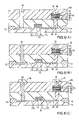
- FIGS. 7(A) to 7(C) are explanatory views showing a conventional method of producing the ferroelectric capacitor.
- a capacitor forming laminated layer 530 is formed on a semiconductor substrate 510 .
- the capacitor forming laminated layer 530 is formed of an interlayer insulating layer 320 , a metal layer 531 , a first conductive layer 533 , a ferroelectric layer 535 , and a second conductive layer 537 , sequentially laminated, respectively.
- the semiconductor substrate 510 is provided with a silicon substrate 511 and an MOSFET 513 formed in an area defined by element separation insulating layers 512 .
- the MOSFET 513 is formed of a drain area 514 , a source area 515 , a gate insulating layer 516 , and a gate electrode 517 .
- the interlayer insulating layer 520 is formed of an oxide layer, and is provided with a conductive plug 524 .
- a hard mask 552 is formed on the capacitor forming laminated layer 530 for covering an area for forming a ferroelectric capacitor with photo-lithography and dry etching.
- the hard mask 552 may be formed of SrRuO 3 (SRO; refer to Patent Reference 1) or lead zirconate titanate (PZT; refer to Patent Reference 2).
- the capacitor forming laminated layer 530 is shaped in a lamination 540 with a desired shape through dry etching using the hard mask 552 .
- a remaining portion of the metal layer 531 becomes a barrier metal 541 ;
- a remaining portion of the first conductive layer 533 becomes a lower electrode 543 ;
- a remaining portion of the ferroelectric layer 535 becomes a ferroelectric layer 545 ;
- a remaining portion of the second conductive layer 537 becomes an upper electrode 547 .
- the lamination 540 becomes the ferroelectric capacitor, and a memory cell of the ferroelectric memory is formed of the second conductive layer 537 and the lamination (the ferroelectric capacitor) 540 .
- Patent Reference 1 U.S. Pat. No. 6,495,413
- Patent Reference 2 U.S. Pat. No. 6,423,592
- a hard mask formed of silicon nitride or titanium nitride is used. Even when such a hard mask is used, it is still necessary to increase a thickness of the hard mask. When the hard mask has a large thickness, a dimension conversion difference increases. The dimension conversion difference has a larger influence as a size of a pattern decreases, thereby making it difficult to obtain a fine pattern necessary for producing a ferroelectric capacitor with high integration density.
- a method of producing a ferroelectric capacitor includes the steps of: preparing a semiconductor substrate; forming a first insulating layer on the semiconductor substrate; laminating sequentially a metal layer, a first conductive layer, a ferroelectric layer, and a second conductive layer on the first insulating layer to form a capacitor forming laminated layer; forming an etching mask forming layer with strontium tantalate or strontium niobate; forming a silicon oxide layer on the etching mask forming layer for covering a ferroelectric capacitor forming area; forming an etching mask through wet etching of the etching mask forming layer with the silicon oxide layer; and forming a lamination formed of a barrier metal, a lower electrode, a ferroelectric layer, and an upper electrode through dry etching of the capacitor forming laminated layer with the etching mask.
- the layer which is difficult to etch through dry etching, is etched through wet etching to form the etching mask for dry etching. Accordingly, it is possible to reduce a thickness of the etching mask and provide a fine pattern.
- FIGS. 1(A) to 1(C) are explanatory views showing a method of producing a ferroelectric capacitor (No. 1 ) according to a first embodiment of the present invention
- FIGS. 2(A) and 2(B) are explanatory views showing a method of producing a ferroelectric capacitor (No. 2 ) according to the first embodiment of the present invention
- FIGS. 3(A) to 3(C) are explanatory views showing a method of producing a ferroelectric capacitor (No. 3 ) according to the first embodiment of the present invention
- FIGS. 4(A) to 4(C) are explanatory views showing a method of producing a ferroelectric capacitor (No. 1 ) according to a second embodiment of the present invention
- FIGS. 5(A) to 5(C) are explanatory views showing a method of producing a ferroelectric capacitor (No. 2 ) according to the second embodiment of the present invention
- FIGS. 6(A) to 6(C) are explanatory views showing a method of producing a ferroelectric capacitor according to a third embodiment of the present invention.
- FIGS. 7(A) to 7(C) are explanatory views showing a conventional method of producing a ferroelectric capacitor.
- FIGS. 1(A)–1(C) to 3 (A)– 3 (C) are explanatory sectional views showing the method of producing a ferroelectric capacitor according to the first embodiment.
- a semiconductor substrate 10 is prepared.
- the semiconductor substrate 10 is provided with a silicon substrate 11 and an MOSFET (metal oxide semiconductor field effect transistor) 13 formed in advance in an area on the silicon substrate 11 defined by an element separation insulating layer 12 .
- the MOSFET 13 is an N-type MOSFET (NMOS)
- the silicon substrate 11 is a P-type substrate.
- a drain area 14 containing a high concentration of N-type impurity (N + -type) and a source area 15 are formed on a surface of the silicon substrate 11 with a predetermined distance in between.
- a gate area 17 is formed on the silicon substrate 11 through a gate insulating layer 16 in an area between the drain area 14 and the source area 15 (see FIG. 1(A) ).
- the area of the silicon substrate 11 between the drain area 14 and the source area 15 becomes a channel forming area, in which a channel (conductive path) connecting between a drain and a source is formed when the NMOS is operated.
- a process of manufacturing the MOSFET has been well known, and a description thereof is omitted.
- a first interlayer insulating layer 20 is deposited on the semiconductor substrate 10 .
- the first interlayer insulating layer 20 is formed as a silicon oxide layer with, for example, a CVD (chemical vapor deposition) method.
- the first interlayer insulating layer 20 is etched with a photolithography, so that a contact hole is formed above the drain area 14 or the source area 15 of the MOSFET 13 (in the embodiment, above the drain area 14 ).
- the contact hole is filled with tungsten with the CVD method to form a conductive plug 24 .
- a surface of the first interlayer insulating layer 20 is flattened with a CMP (chemical mechanical polishing) method (see FIG. 1(B) ).
- CMP chemical mechanical polishing
- a metal layer 31 , a first conductive layer 33 , a ferroelectric layer 35 , and a second conductive layer 37 are sequentially laminated on the first insulating layer 20 to form a capacitor forming laminated layer 30 .
- the metal layer 31 is formed of a material selected from one of titanium nitride, aluminum nitride, or tantalum nitride.
- the metal layer 31 is formed on the first interlayer insulating layer 20 with a sputtering method.
- the first conductive layer 33 is formed of a material selected from one of platinum, iridium, ruthenium, or iridium oxide; or is formed as a laminated layer formed of more than two of the materials described above.
- the first conductive layer 33 is formed on the metal layer 31 with the sputtering method.
- the ferroelectric layer 35 is formed of a material selected from lead zirconate titanate, strontium bismuth tantalate, bismuth titanate, or bismuth lanthanum titanate according to a purpose and specification.
- the second conductive layer 37 is formed of a material selected from one of platinum, iridium, ruthenium, or iridium oxide; or is formed as a laminated layer formed of more than two of the materials described above.
- An etching mask forming layer 39 formed of strontium tantalate or strontium niobate is then formed on the second conductive layer 37 of the capacitor forming laminated layer 30 with the CVD method (see FIG. 1(C) ).
- the metal layer 31 is formed of a titanium nitride layer with a thickness of 25 nm.
- the first conductive layer 33 is a laminated layer formed of a platinum layer with a thickness of 50 nm, an iridium oxide layer with a thickness of 100 nm, and an iridium layer with a thickness of 100 nm.
- the ferroelectric layer 35 is formed of a strontium bismuth tantalate layer with a thickness of 120 nm.
- the second conductive layer 37 is formed of a platinum layer with a thickness of 100 nm.
- the etching mask forming layer 39 is formed of a strontium tantalate layer with a thickness of 100 nm.
- an etching mask 49 formed of strontium tantalate is formed through the wet etching with the silicon oxide layer mask 52 (see FIG. 3(B) ).
- a mixture of nitric acid, fluorinated acid, and acetic acid is used as an etchant of the wet etching. It is difficult to etch strontium tantalate through the dry etching. However, strontium tantalate is soluble in a mixture of nitric acid, fluorinated acid, and acetic acid for the following reason.
- Strontium tantalate SrTa 2 O 6 is a composite oxide crystal of tantalum oxide Ta 2 O 5 and strontium oxide SrO. Tantalum oxide Ta 2 O 5 is converted to water-soluble tantalate hexafluoride HTaF 6 through the following reaction. SrO+12HF ⁇ 2HTaF 6 +5H 2 O Strontium oxide SrO reacts with water to yield strontium hydroxide Sr(OH) 2 through the following reaction. SrO+H 2 O ⁇ Sr(OH) 2 Strontium hydroxide Sr(OH) 2 is highly soluble in acid.
- the mixture of nitric acid, fluorinated acid, and acetic acid contains 2 to 95 weight % of 60% nitric acid aqueous solution, 5 to 98 weight % of 50% fluorinated acid aqueous solution, and 5 to 70 weight % of glacial acetic acid.
- the etchant may contain only nitric acid and fluorinated acid without glacial acetic acid. It is preferable to use glacial acetic acid for suppressing decomposition of nitric acid.
- the capacitor forming laminated layer 30 is etched through the RIE with the etching mask 49 to form a lamination 40 as a ferroelectric capacitor. It takes a very long time to etch the etching mask 49 formed of strontium tantalate through the RIE, so that the etching mask 49 withstands as a mask during the RIE. Accordingly, during the RIE, it is necessary only to replace a gas without reproducing the mask to form the ferroelectric capacitor.
- the first and second conductive layers 33 and 37 are etched under a Cl 2 —O 2 type gas
- the ferroelectric layer 35 is etched under a Cl 2 —Ar type gas
- the metal layer 31 is etched under a BCl 3 —Cl 2 type gas.
- a remaining portion of the metal layer 31 after the etching becomes a barrier metal 41 , and a remaining portion of the first conductive layer 33 after the etching becomes a lower electrode 43 .
- a remaining portion of the ferroelectric layer 35 after the etching becomes a ferroelectric layer 45 , and a remaining portion of the second conductive layer 37 after the etching becomes an upper electrode 47 .
- the barrier metal 41 is provided for preventing a reaction between a plug material of the conductive plug 24 and an electrode material of the lower electrode 43 .
- the silicon oxide layer mask 52 used in the wet etching is removed during the RIE. After the lamination (ferroelectric capacitor) 40 is formed through the RIE, the etching mask 49 remains and has a thickness of 25 nm (see FIG. 3(C) ).
- An etching rate of strontium tantalate relative to the lower and upper electrodes 42 and 47 during the dry etching is called selectivity, and it is possible to make the selectivity more than 4. Further, it is possible to make the dry etching selectivity of strontium tantalate relative to the ferroelectric layer 45 more than 3.
- FIGS. 4(A)–4(B) and 5 (A)– 5 (B) are explanatory sectional views showing the method of producing a ferroelectric capacitor according to the second embodiment of the present invention.
- a process up to the step in which the lamination 40 is formed through the RIE is the same as that of the first embodiment shown in FIGS. 1(A) to 3(B) , and descriptions thereof are omitted.
- the lamination 40 and the etching mask 49 are embedded in a second interlayer insulating layer 60 having a relatively large thickness without removing the etching mask 49 formed of strontium tantalate (see FIG. 4(A) ).
- the second interlayer insulating layer 60 is formed of a silicon oxide layer with the CVD method.
- a resist formed of an organic resin is applied on the second interlayer insulating layer 60 to form a photo-resist layer (not shown).
- a pattern is formed with a known lithography, so that a photo-resist pattern (not shown) is formed to have an opening in a contact hole forming area of the second interlayer insulating layer 60 .
- the second interlayer insulating layer 60 is etched through the dry etching with the photo-resist pattern as a mask to form a contact hole 62 in the second interlayer insulating layer 60 (see FIG. 4(B) ).
- the etching mask 49 formed of strontium tantalate is hardly etched under the etching condition of the second interlayer insulating layer 60 formed of silicon oxide, and functions as an etching stop.
- the etching mask 49 is etched through the wet etching with the second interlayer insulating layer 60 having the contact hole 62 as a mask to form a contact hole 64 in the etching mask 49 (see FIG. 4(C) ).
- Etching conditions of the step such as an etchant are the same as those of the wet etching in which the etching mask 49 is formed as shown in FIG. 3(B) , and descriptions thereof are omitted.
- a contact hole 66 is formed in the first interlayer insulating layer 20 and the second interlayer insulating layer 60 above the drain area 14 or the source area 15 (in the embodiment, above the source area 15 ; see FIG. 5(A) ).
- the contact holes 62 , 64 , and 66 are filled with tungsten with the CVD method to form conductive plugs 26 and 28 (see FIG. 5(B) ).
- a metal (aluminum) wiring 70 is formed on the conductive plugs 26 and 28 formed in the second interlayer insulating layer 60 with the sputtering method (see FIG. 5(C) ).
- the MOSFET 13 and the lamination (ferroelectric capacitor) 40 are electrically connected to an external device through the metal wiring 70 .
- the contact holes in the lamination 40 are formed sequentially through the dry etching and the wet etching.
- the etching mask 49 functions as the etching stop. Accordingly, when the contact hole is formed through the dry etching, it is possible to reduce physical damage due to an electrical field stress such as charging or chemical damage due to a reducing gas passing through the upper electrode against the ferroelectric capacitor.
- FIGS. 6(A) to 6(C) are explanatory views showing the method of producing a ferroelectric capacitor according to the third embodiment of the present invention. Except that a conductive plug 25 and a bit wire 27 are provided in the first interlayer insulating layer 20 , a process up to the step in which the lamination 40 and the etching mask 49 are embedded in the second interlayer insulating layer 60 is the same as that of the second embodiment shown in FIG. 4(A) , and descriptions thereof are omitted.
- a resist formed of an organic resin is applied on the second interlayer insulating layer 60 to form a photo-resist layer (not shown).
- a pattern is formed with a known lithography, so that a photo-resist pattern (not shown) is formed to have an opening in a contact hole forming area of the second interlayer insulating layer 60 .
- the second interlayer insulating layer 60 is etched through the dry etching with the photo-resist pattern as a mask to form a contact hole 63 in the second interlayer insulating layer 60 (see FIG. 6(A) ).
- the etching mask 49 formed of strontium tantalate is hardly etched under the etching conditions of the second interlayer insulating layer 60 formed of silicon oxide, and functions as an etching stop.
- the etching mask 49 is etched through the wet etching with the second interlayer insulating layer 60 having the contact hole 63 as a mask to form a contact hole 65 in the etching mask 49 (see FIG. 6(B) ).
- the contact holes 63 and 65 have an areal ratio relative to an area of the ferroelectric capacitor 40 larger than that in the second embodiment.
- an opening of the contact hole is about 0.8 ⁇ m square relative to the capacitor having a size of 1.0 ⁇ m square, and has an area more than nine times larger than that in the second embodiment.
- aluminum is formed in a film at a high temperature to form a metal wiring 72 filled in the contact holes 63 and 65 (see FIG. 6(C) ).
- the third embodiment it is possible to reduce an aspect ratio of the contact hole. Accordingly, it is not necessary to form the conductive plug filled with tungsten through the CVD method, thereby reducing deterioration of the ferroelectric capacitor due to reduction. That is, it is possible to eliminate the process causing the reduction deterioration after the lamination or ferroelectric capacitor 40 is formed, thereby making it possible to produce the ferroelectric capacitor with high reliability.
Abstract
Description
SrO+12HF→2HTaF6+5H2O
Strontium oxide SrO reacts with water to yield strontium hydroxide Sr(OH)2 through the following reaction.
SrO+H2O→Sr(OH)2
Strontium hydroxide Sr(OH)2 is highly soluble in acid.
Claims (12)
Applications Claiming Priority (2)
| Application Number | Priority Date | Filing Date | Title |
|---|---|---|---|
| JP2004220156A JP4318607B2 (en) | 2004-07-28 | 2004-07-28 | Method for manufacturing ferroelectric capacitor |
| JP2004-243520 | 2004-08-24 |
Publications (2)
| Publication Number | Publication Date |
|---|---|
| US20060046315A1 US20060046315A1 (en) | 2006-03-02 |
| US7157288B2 true US7157288B2 (en) | 2007-01-02 |
Family
ID=35905912
Family Applications (1)
| Application Number | Title | Priority Date | Filing Date |
|---|---|---|---|
| US11/105,439 Expired - Fee Related US7157288B2 (en) | 2004-07-28 | 2005-04-14 | Method of producing ferroelectric capacitor |
Country Status (2)
| Country | Link |
|---|---|
| US (1) | US7157288B2 (en) |
| JP (1) | JP4318607B2 (en) |
Cited By (1)
| Publication number | Priority date | Publication date | Assignee | Title |
|---|---|---|---|---|
| US8451308B2 (en) | 2009-07-31 | 2013-05-28 | Ricoh Company, Ltd. | Image forming apparatus |
Families Citing this family (3)
| Publication number | Priority date | Publication date | Assignee | Title |
|---|---|---|---|---|
| JP4621081B2 (en) * | 2005-07-07 | 2011-01-26 | Okiセミコンダクタ株式会社 | Manufacturing method of semiconductor device |
| JP4838613B2 (en) * | 2006-03-28 | 2011-12-14 | 富士通セミコンダクター株式会社 | Manufacturing method of semiconductor device |
| JP2009071241A (en) * | 2007-09-18 | 2009-04-02 | Seiko Epson Corp | Semiconductor device, and manufacturing method thereof |
Citations (6)
| Publication number | Priority date | Publication date | Assignee | Title |
|---|---|---|---|---|
| US5532182A (en) * | 1993-12-28 | 1996-07-02 | Hyundai Electronics Industries Co., Ltd. | Method for fabricating stacked capacitor of a DRAM cell |
| US6423592B1 (en) | 2001-06-26 | 2002-07-23 | Ramtron International Corporation | PZT layer as a temporary encapsulation and hard mask for a ferroelectric capacitor |
| US6495413B2 (en) | 2001-02-28 | 2002-12-17 | Ramtron International Corporation | Structure for masking integrated capacitors of particular utility for ferroelectric memory integrated circuits |
| US20030143853A1 (en) | 2002-01-31 | 2003-07-31 | Celii Francis G. | FeRAM capacitor stack etch |
| US6753247B1 (en) * | 2002-10-31 | 2004-06-22 | Advanced Micro Devices, Inc. | Method(s) facilitating formation of memory cell(s) and patterned conductive |
| US20050101034A1 (en) * | 2003-11-10 | 2005-05-12 | Sanjeev Aggarwal | Hardmask for forming ferroelectric capacitors in a semiconductor device and methods for fabricating the same |
-
2004
- 2004-07-28 JP JP2004220156A patent/JP4318607B2/en not_active Expired - Fee Related
-
2005
- 2005-04-14 US US11/105,439 patent/US7157288B2/en not_active Expired - Fee Related
Patent Citations (6)
| Publication number | Priority date | Publication date | Assignee | Title |
|---|---|---|---|---|
| US5532182A (en) * | 1993-12-28 | 1996-07-02 | Hyundai Electronics Industries Co., Ltd. | Method for fabricating stacked capacitor of a DRAM cell |
| US6495413B2 (en) | 2001-02-28 | 2002-12-17 | Ramtron International Corporation | Structure for masking integrated capacitors of particular utility for ferroelectric memory integrated circuits |
| US6423592B1 (en) | 2001-06-26 | 2002-07-23 | Ramtron International Corporation | PZT layer as a temporary encapsulation and hard mask for a ferroelectric capacitor |
| US20030143853A1 (en) | 2002-01-31 | 2003-07-31 | Celii Francis G. | FeRAM capacitor stack etch |
| US6753247B1 (en) * | 2002-10-31 | 2004-06-22 | Advanced Micro Devices, Inc. | Method(s) facilitating formation of memory cell(s) and patterned conductive |
| US20050101034A1 (en) * | 2003-11-10 | 2005-05-12 | Sanjeev Aggarwal | Hardmask for forming ferroelectric capacitors in a semiconductor device and methods for fabricating the same |
Cited By (1)
| Publication number | Priority date | Publication date | Assignee | Title |
|---|---|---|---|---|
| US8451308B2 (en) | 2009-07-31 | 2013-05-28 | Ricoh Company, Ltd. | Image forming apparatus |
Also Published As
| Publication number | Publication date |
|---|---|
| US20060046315A1 (en) | 2006-03-02 |
| JP2006041246A (en) | 2006-02-09 |
| JP4318607B2 (en) | 2009-08-26 |
Similar Documents
| Publication | Publication Date | Title |
|---|---|---|
| US20090068763A1 (en) | Method for manufacturing semiconductor device and its manufacturing method | |
| JP5502302B2 (en) | Semiconductor device and manufacturing method thereof | |
| US11729993B2 (en) | Ferroelectric random access memory (FRAM) capacitors and methods of construction | |
| US20060043452A1 (en) | Ferroelectric memory and its manufacturing method | |
| JP2009071022A (en) | Manufacturing method of semiconductor device, and semiconductor device | |
| US20240114698A1 (en) | Semiconductor device | |
| JP4838613B2 (en) | Manufacturing method of semiconductor device | |
| JP4445446B2 (en) | Manufacturing method of semiconductor device | |
| WO2021055009A1 (en) | Ferroelectric memory devices with dual dielectric confinement and methods of forming the same | |
| US7157288B2 (en) | Method of producing ferroelectric capacitor | |
| US7547638B2 (en) | Method for manufacturing semiconductor device | |
| US20040169211A1 (en) | Avoiding shorting in capacitors | |
| EP1387405A2 (en) | Semiconductor memory device and method for manufacturing the same | |
| JP3166746B2 (en) | Capacitor and method of manufacturing the same | |
| US7507662B2 (en) | Ferroelectric memory and its manufacturing method | |
| JP2001308288A (en) | Manufacturing method of semiconductor device, and semiconductor device | |
| JP5412785B2 (en) | Semiconductor device and manufacturing method thereof | |
| US7094611B1 (en) | Method of producing ferroelectric capacitor | |
| US20230345735A1 (en) | Ferroelectric random access memory (fram) capacitors and methods of construction | |
| JP2008305960A (en) | Manufacturing method of ferroelectric capacitor, and ferroelectric capacitor | |
| JP2009071141A (en) | Manufacturing method of ferroelectric memory device, and ferroelectric memory device | |
| KR100801202B1 (en) | Process for fabricating semiconductor device | |
| KR100866709B1 (en) | Manufacturing method for capacitor of semiconductor device | |
| KR100722940B1 (en) | Method for fabricating semiconductor device | |
| CN116686431A (en) | Ferroelectric Random Access Memory (FRAM) capacitor and method of construction |
Legal Events
| Date | Code | Title | Description |
|---|---|---|---|
| AS | Assignment |
Owner name: OKI ELECTRIC INDUSTRY CO., LTD., JAPAN Free format text: ASSIGNMENT OF ASSIGNORS INTEREST;ASSIGNOR:ITO, TOSHIO;REEL/FRAME:016479/0252 Effective date: 20050326 |
|
| CC | Certificate of correction | ||
| FEPP | Fee payment procedure |
Free format text: PAYOR NUMBER ASSIGNED (ORIGINAL EVENT CODE: ASPN); ENTITY STATUS OF PATENT OWNER: LARGE ENTITY |
|
| AS | Assignment |
Owner name: OKI SEMICONDUCTOR CO., LTD., JAPAN Free format text: CHANGE OF NAME;ASSIGNOR:OKI ELECTRIC INDUSTRY CO., LTD.;REEL/FRAME:022092/0903 Effective date: 20081001 Owner name: OKI SEMICONDUCTOR CO., LTD.,JAPAN Free format text: CHANGE OF NAME;ASSIGNOR:OKI ELECTRIC INDUSTRY CO., LTD.;REEL/FRAME:022092/0903 Effective date: 20081001 |
|
| FPAY | Fee payment |
Year of fee payment: 4 |
|
| AS | Assignment |
Owner name: LAPIS SEMICONDUCTOR CO., LTD., JAPAN Free format text: CHANGE OF NAME;ASSIGNOR:OKI SEMICONDUCTOR CO., LTD;REEL/FRAME:032495/0483 Effective date: 20111003 |
|
| REMI | Maintenance fee reminder mailed | ||
| LAPS | Lapse for failure to pay maintenance fees | ||
| STCH | Information on status: patent discontinuation |
Free format text: PATENT EXPIRED DUE TO NONPAYMENT OF MAINTENANCE FEES UNDER 37 CFR 1.362 |
|
| FP | Lapsed due to failure to pay maintenance fee |
Effective date: 20150102 |