US7158841B1 - Active DC output control and method for controlling targeted applications - Google Patents
Active DC output control and method for controlling targeted applications Download PDFInfo
- Publication number
- US7158841B1 US7158841B1 US10/831,508 US83150804A US7158841B1 US 7158841 B1 US7158841 B1 US 7158841B1 US 83150804 A US83150804 A US 83150804A US 7158841 B1 US7158841 B1 US 7158841B1
- Authority
- US
- United States
- Prior art keywords
- signal
- input
- output
- coupled
- scaled
- Prior art date
- Legal status (The legal status is an assumption and is not a legal conclusion. Google has not performed a legal analysis and makes no representation as to the accuracy of the status listed.)
- Active, expires
Links
Images


Classifications
-
- H—ELECTRICITY
- H02—GENERATION; CONVERSION OR DISTRIBUTION OF ELECTRIC POWER
- H02M—APPARATUS FOR CONVERSION BETWEEN AC AND AC, BETWEEN AC AND DC, OR BETWEEN DC AND DC, AND FOR USE WITH MAINS OR SIMILAR POWER SUPPLY SYSTEMS; CONVERSION OF DC OR AC INPUT POWER INTO SURGE OUTPUT POWER; CONTROL OR REGULATION THEREOF
- H02M3/00—Conversion of dc power input into dc power output
- H02M3/02—Conversion of dc power input into dc power output without intermediate conversion into ac
- H02M3/04—Conversion of dc power input into dc power output without intermediate conversion into ac by static converters
- H02M3/10—Conversion of dc power input into dc power output without intermediate conversion into ac by static converters using discharge tubes with control electrode or semiconductor devices with control electrode
- H02M3/145—Conversion of dc power input into dc power output without intermediate conversion into ac by static converters using discharge tubes with control electrode or semiconductor devices with control electrode using devices of a triode or transistor type requiring continuous application of a control signal
- H02M3/155—Conversion of dc power input into dc power output without intermediate conversion into ac by static converters using discharge tubes with control electrode or semiconductor devices with control electrode using devices of a triode or transistor type requiring continuous application of a control signal using semiconductor devices only
- H02M3/156—Conversion of dc power input into dc power output without intermediate conversion into ac by static converters using discharge tubes with control electrode or semiconductor devices with control electrode using devices of a triode or transistor type requiring continuous application of a control signal using semiconductor devices only with automatic control of output voltage or current, e.g. switching regulators
- H02M3/157—Conversion of dc power input into dc power output without intermediate conversion into ac by static converters using discharge tubes with control electrode or semiconductor devices with control electrode using devices of a triode or transistor type requiring continuous application of a control signal using semiconductor devices only with automatic control of output voltage or current, e.g. switching regulators with digital control
Definitions
- the invention relates generally to integrated circuit design, and more particularly to an integrated circuit for generating a voltage signal used to control a parameter of an application being monitored.
- the present invention provides a feedback control-loop system that employs an active DC output control circuit which compares an input parameter measurement against a target specification associated with the input parameter measurement.
- the active DC output control circuit controls a temperature for laser bias adjustment.
- the active DC output control circuit controls a motor speed input from a source, such as a tachometer, for motor speed adjustment.
- the active DC output control circuit controls a power amplifier for wireless applications. Other applications are possible as one knowledgeable in the art will understand and as mentioned in the prior art.
- a system-on-a-chip comprises a digital-to-analog converter for receiving an analog input parameter signal, the digital-to-analog converter scaling the analog signal by a factor stored on the chip; a buffer for buffering the signal from the DAC and a filter coupled to the output of the buffer for filtering the buffered, scaled analog signal to produce a filtered, buffered, scaled signal; a comparator having a first input for receiving a target specification associated with the input parameter measurement and having a second input for receiving the filtered, buffered, scaled signal, the comparator comparing the target specification with the filtered, buffered, scaled signal; and a logic circuit for increasing the output signal if the value of the filtered signal is less than the input parameter and for decreasing the output signal if the value of the filtered signal is greater than the input parameter for a positive polarity case.
- the filtered signal is increased or decreased by the ADOCTM, active DC output control circuit, adjusting its control voltage output, ( 113 of FIG. 1 ) to the input trim pin ( 121 of FIG. 1 ) of the application being controlled, thus producing a change in the signal parameter being sensed by the ADOCTM.
- the present invention enables a system to achieve a desired parameter at the output load within a narrow voltage margin of a DC/DC converter array.
- a non-volatile memory in the active DC output control circuit stores multiple values of desired output voltages including nominal and test values for the array loads, including scaling factors and shifting levels and polarities.
- FIG. 1 is an architectural diagram illustrating a first embodiment of a control loop system that employs an active DC output control for a single load, in this case a DC/DC converter, in accordance with the present invention.
- FIG. 2 is an architectural diagram illustrating a second embodiment of a control loop system that employs an active DC output control for multiple loads in accordance with the present invention.
- FIG. 3A is more detailed block diagram illustrating the control loop system 300 with an active DC output control for a single load in accordance with the present invention.
- FIG. 3B is a circuit diagram of the input voltage sensing and signal conditioning circuit in accordance with one embodiment of the present invention.
- FIG. 4 is a more detailed block diagram illustrating the control loop system 400 with an active DC output control for multiple loads in accordance with the present invention.
- FIG. 5 is a flow diagram illustrating the process for monitoring an active DC output control loop in accordance with one embodiment of the present invention using a DC/DC converter as the target application.
- FIG. 6 is a general architectural diagram illustrating an active DC output controller for monitoring, adjusting, and maintaining a specific input parameter from an application in accordance with an embodiment of the present invention.
- FIG. 7 is an architectural diagram illustrating an embodiment for implementing the active DC output controller for laser bias adjustment in accordance with the present invention.
- FIG. 8 is an architectural diagram illustrating an embodiment for implementing the active DC output controller for motor speed adjustment in accordance with the present invention.
- FIG. 9 is an architectural diagram illustrating an embodiment for implementing the active DC output controller for power amplifier adjustment in wireless applications in accordance with the present invention.
- FIG. 1 there is shown an architectural diagram illustrating a first embodiment of a control loop system plus application 100 with an active DC output control for a single load.
- the control loop system plus application 100 comprises an active DC output control circuit 110 having a NV (non-volatile) memory 111 , which in turn is connected to a DC/DC converter 120 , which in turn is connected to a single port load 130 , collectively ( 120 + 130 ), the application.
- a control pin 113 from the active DC output control circuit 110 is connected to an input trim pin 121 of the DC/DC converter 120 .
- the V+ input 131 is commonly connected to a Vsense 112 of the active DC output control circuit 110 , a V+ 122 of the DC/DC converter 120 , and a S+ 123 of the DC/DC converter 120 .
- the V ⁇ input 132 is commonly connected to a ground 114 of the active DC output control circuit 110 , a V ⁇ 124 of the DC/DC converter 120 , and a S ⁇ 125 of the DC/DC converter 120 .
- An objective of the active DC output control circuit 110 is to precisely regulate the voltage difference between V+ 131 and V ⁇ 132 at the load 130 .
- the load 130 can be either a single load or multiple loads, which is shown and further described with respect to FIG. 2 .
- FIG. 2 there is shown an architectural diagram illustrating a second embodiment of a control loop system 200 that employs an active DC output control for multiple port loads.
- the control loop system 200 comprises an active DC output control circuit 210 having a NV memory 211 and having multiple trim pins: a control pin 0 ( 213 ) through a control pin N ( 215 ).
- the control pin 0 ( 213 ) from the active DC output control circuit 210 is connected to a trim pin 221 of a first DC/DC converter 220 , which in turn has a set of V+ 222 and S+ 223 pins that are connected to a V+ 241 pin in a first load 240 , and a set of V ⁇ 224 and S ⁇ 225 coupled to a V ⁇ 242 pin in the first load 240 .
- the control pin N ( 215 ) from the active DC output control circuit 210 is coupled to a trim pin 231 in Nth DC/DC converter 230 , which in turn has a set of V+ 232 and S+ 233 pins connected to a V+ 251 pin of Nth load 250 , and a set of V ⁇ 234 and S ⁇ 235 connected to a V ⁇ 252 pin in the Nth load 250 .
- additional DC/DC converters are positioned between the first DC/DC converter 220 and the Nth DC/DC converter 230 , as well as additional loads are positioned between the first load 240 and the Nth load 250 .
- the active DC output control circuit 210 has a Vsense 0 ( 212 ) coupled to the V+ 241 of the first load 240 , a Vsense N ( 214 ) coupled to the V+ 251 of the N load 250 , and a ground 216 coupled commonly to the first load 240 through the Nth load 250 .
- the active DC output control circuit 210 uses the control 0 pin ( 213 ) to precisely regulate the V+ 241 input at the first load 240 , and uses the control Nth pin 213 to precisely regulate the V+ 251 input at the Nth load 250 . Additional trim pins in the active DC output control circuit 210 are positioned to precisely regulate additional DC/DC converters and loads as schematically shown.
- the control loop system plus applications 200 contains a 3.3V DC/DC converter in the first DC/DC converter 220 and a 2.5V DC/DC converter in the Nth DC/DC converter 230 , the user may need to test all load components with those supplies raised by 5%.
- the active DC output control circuit 210 measures the voltage output V+ 241 generated from the 3.3V DC/DC converter 220 , compared with a first reference voltage, and adjusts the voltage output slightly upward by adjusting the voltage on the control pin 0 ( 213 ).
- the active DC output control circuit 210 then switches to the next DC/DC Converter which has been programmed into the non-volatile memory ( 211 ) of active DC output control circuit 210 through a serial interface line (not shown) and read by the control logic ( 320 ). Any combination of the first through Nth DC/DC converters may be programmed to be controlled or bypassed. Eventually the sequence will step to the 2.5V DC/DC converter in the Nth DC/DC converter ( 230 ) position and perform the same operation or skip as the pre-programmed instructions indicate. This process is repeated until all selected supplies are at the desired output levels of nominal plus 5%. The active DC output control circuit 210 then maintains the desired output level.
- the active DC output control circuit 210 senses the change and makes slight adjustments to the trim pin until the output is back at the set point. When testing is completed, the active DC output control circuit 210 can be disconnected to allow the DC/DC converter to return to its nominal output. Alternatively, the active DC output control circuit 210 can be re-programmed to the desired nominal output values for the converters and left connected to the trim pins. This can provide a more accurate DC output level than the converters would normally provide.
- FIG. 3A is a more detailed block diagram 300 illustrating the active DC output control circuit 110 for a single application.
- An input voltage sensing and signal conditioning circuit 310 comprises a digital-analog-converter DAC circuit 311 , coupled to a unity gain amplifier 312 , functioning as the buffer, and a filter 313 , as shown in FIG. 3B .
- the input voltage sensing and signal conditioning circuit ( 310 ) receives a sense+ signal ( 305 ) and a sense ⁇ signal 306 into the DAC 311 .
- the sense ⁇ signal is typically a common ground as noted in FIG. 2 ( 216 ).
- DAC ( 311 ) scales the analog signal ( 305 ) by a digital factor received from the control logic ( 320 ) and stored in NV Memory ( 330 ).
- the analog sense signal would be divided by 1024, equivalent to 10 bits, and then multiplied by the scaling factor, for instance 512 if a 50% scaling had been chosen.
- the DAC were eight bits, 256 would be the divisor and a scaling from 0/256 to 255/256 could be achieved.
- the now scaled signal passes to the unity gain amplifier ( 312 ) and then through the filter ( 313 ).
- the input voltage sensing and signal conditioning circuit 310 generates a scaled/buffered/filtered (V s/b/f ) signal ( 315 ) to a comparator ( 350 ).
- the comparator ( 350 ) compares the scaled/buffered/filtered (V s/b/f ) signal ( 315 ) with a reference (V ref ) signal ( 341 ) that propagates through a Vref level shifter ( 340 ) into the comparator ( 350 ).
- the level shifter quantity is determined by instructions from the control logic unit ( 320 ) which reads the V ref shift value stored in NV Memory ( 330 )
- the output control circuit ( 360 ) adjusts the voltage on the ADOCTM control pin ( 371 ), or ( 113 ), slightly upward to increase the trim voltage ( 121 ) and subsequently V+ ( 122 ).
- the output control circuit ( 360 ) adjusts the voltage on the ADOCTM control pin ( 371 ), or ( 113 ), slightly lower to decrease the trim voltage ( 121 ) and subsequently lower V+ ( 122 ).
- the output control circuit ( 360 ) adjusts the voltage on ADOCTM control pin ( 371 ), or ( 113 ), slightly downward to decrease the trim voltage ( 121 ) and subsequently increase V+ ( 122 ).
- V ref ( 341 ) is supplied from a source internal to the ADOCTM chip (not shown) or, alternatively, by the user; typical values are in the 1.25 volt range but higher or lower may be used depending upon the application.
- NV Memory 330
- This information is then used by control logic ( 320 ) to determine the polarity for adjusting output control circuit ( 360 ).
- Control logic ( 320 ) allows the user to interface with the application, in this case a DC/DC converter ( 120 ).
- the control logic ( 320 ) controls the digital scaling data going to the DAC ( 311 ) and the Vref level shifter ( 340 ).
- the control logic ( 320 ) controls the sequence of events that occurs in the active DC output control circuit ( 110 ).
- the control logic ( 320 ) is coupled to NV Memory ( 330 ) that stores the data for the DAC ( 311 ) and Vref level shifter ( 340 ).
- the output signal ( 371 ) generated by the output control circuit ( 360 ) can be either a voltage signal or current signal as previously programmed into the control logic 320 . Conversion to current requires the addition of a “voltage-to-current” conversion capability either externally as shown in FIG. 7 (VOI- 740 ) or internally on the ADOCTM chip itself (not shown).
- a scaling higher than 1 can be achieved, if desired, by adjusting the reference voltage such that a higher output than a normal 100% full scale might be achieved. For instance, on a DC/DC converter application, if a Vsense ( 305 ) coming in is indicating the converter is at its rated 5 volt output and, for purposes of this example, the scaling is set to 50%, the (V s/b/f ) signal ( 315 ) sent to the comparator ( 350 ) will be 2.5 volts. If the Vref chosen to correspond to a 5 volt output is also 2.5 volts and the level shifter is set to 1.0, then no adjustment will occur by the output control circuit ( 360 ).
- the output control circuit ( 360 ) will increase the trim voltage until 5.25 volts is on the sense line ( 305 ) and the (V s/b/f ) signal ( 315 ) sent to the comparator ( 350 ) will be 2.625 volts.
- FIG. 4 is a more detailed block diagram ( 400 ) illustrating the active DC output control circuit 210 with an active DC output control for multiple applications.
- a n:1 mux ( 405 ) multiplexes multiple sense signals ranging from a sense+( 0 ) ( 410 ) signal, a sense+( 1 ) ( 411 ) signal, up to a sense+(n) ( 416 ) signal into an input voltage sensing and signal conditioning circuit ( 420 ).
- (n) may be as large as practical, for instance 6 or 256 or higher.
- the input voltage sensing and signal conditioning circuit ( 420 ) comprises the digital-to-analog converter DAC circuit ( 311 ), coupled to the unity gain amplifier, or buffer, ( 312 ) and the filter ( 313 ), as shown in FIG. 3B .
- the n:1 mux ( 405 ) transmits an output signal ( 417 ) from a selected signal among the sense+( 0 ) ( 410 ) signal, the sense+( 1 ) ( 411 ) signal, up to and including the sense+(n) ( 416 ) to the input voltage sensing and signal conditioning circuit ( 420 ); the selection is based upon instructions from the control logic circuit ( 430 ) as previously programmed and stored in NV Memory ( 440 ).
- the input voltage sensing and signal conditioning circuit ( 420 ) processes the signal ( 417 ) through the DAC ( 311 ), the unity gain amplifier ( 312 ), the filter ( 313 ), and generates a scaled/buffered/filtered (V s/b/f ) signal ( 421 ).
- a comparator ( 460 ) receives the scaled/buffered/filtered signal ( 421 ) from the input voltage sensing and signal conditioning circuit ( 420 ) and compares with a reference, V ref , signal ( 451 ) after it propagates through a Vref level shifter ( 450 ). All relationships for multiple applications are analogous to the description for single application operation described previously.
- Control logic ( 430 ) has a serial interface input (not shown) over which the user programs the sequence of starting or stopping the activity for each application and turning a particular application “on” or “off”; this information is also stored in NV Memory ( 440 ) and may be updated in real time in one embodiment. All data stored in the NV Memory ( 440 ) is transmitted via the serial port of the control logic portion. Other communication methods than a serial interface are feasible as one knowledgeable in the field is aware. Note that in the multiple application case the Sense ⁇ signal is taken to be a common ground (not shown); an additional n:1 multiplexer is not required for that signal.
- An output control circuit ( 470 ) is connected to the comparator ( 460 ) for increasing or decreasing the voltage output using the results of the comparator ( 460 ) and the polarity of a given application as stored in NV Memory ( 440 ) and transmitted by control logic circuit ( 430 ).
- a 1:n mux ( 480 ) selects the appropriate trim drive among a trim drive( 0 ) ( 490 ), up to a trim drive(n) ( 495 ).
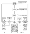
- FIG. 5 is a flow diagram ( 500 ) illustrating the process for actively controlling the DC output of given application, in this case a DC/DC converter.
- the active DC output control circuit ( 110 ), ( 210 ) or ( 400 ) will react depending on whether the application, in this case a DC/DC converter, has a positive polarity or a negative polarity.
- FIG. 5 shows the logical steps of the ADOCTM as described previously.
- FIG. 6 there is shown a general architectural diagram illustrating an alternative active DC output controller ( 600 ) for monitoring, adjusting, and maintaining a specific input parameter from an application ( 605 ) with a feedback control-loop that generates an output signal ( 690 ) for adjustment to the specific application ( 605 ) in accordance with an embodiment of the present invention.
- Certain elements of the basic ADOCTM circuit as shown in FIG. 3A have been omitted and certain other elements have been expanded for clarifying purposes.
- the active DC output control ( 600 ) comprises a DAC, digital-to-analog converter, 620 , a buffer 630 , a filter 640 , a comparator 650 , a logic circuit 660 , a first current source 670 , a second current source 675 , a capacitor 677 , and a buffer 680 .
- the DAC 620 receives an input parameter measurement signal 610 from a source, such as a sensor 606 or, alternatively, directly from the application 605 .
- the DAC 620 scales the input parameter measurement signal 610 , the buffer 630 buffers the input parameter measurement signal 610 , and the filter 640 filters the input parameter measurement signal 610 .
- the filter 640 comprises a resistor having a first end connected to an output of the buffer 630 , a second end connected commonly to a capacitor 642 , and a negative input of the comparator 650 .
- the comparator 650 compares the filtered, buffered, scaled input parameter measurement signal 643 received through the negative input of the comparator 650 with a target parameter specification 645 received through a positive input of the comparator 650 .
- the logic circuit 660 increases the voltage on node 676 if the filtered input parameter measurement 643 is lower than the target parameter specification 645 , and decreases the voltage on node 676 if the filtered input parameter measurement 643 is higher than the target parameter specification 645 ; the changes on node 676 are reflected in similar action by the input parameter measurement 643 .
- the logic circuit 660 in turn increases the voltage at a node 676 if the adjustment is to increase an output control signal 690 or decreases the voltage at the node 676 if the adjustment is to decrease the output control signal 690 .
- the buffer 680 buffers the output received from the logic circuit 660 before generating the output calibration signal 690 . This sequence of actions is for a positive polarity application.
- the general architecture of the active DC output controller 600 can be applied to various applications for sensing a parameter, such as a temperature, a motor speed, a power amplifier level, where a feedback control-loop compares an input parameter measurement signal with a reference signal for a specific application for adjusting an output control signal to meet the target parameter specification associated with the input parameter measurement signal.
- a parameter such as a temperature, a motor speed, a power amplifier level
- FIG. 7 there is shown an architectural diagram 700 illustrating one embodiment for implementing the active DC output controller, ADOCTM, ( 110 ), ( 210 ), ( 300 ), ( 400 ), for laser bias adjustment in accordance with the present invention.
- the partial active DC output control schematic as shown in FIG. 6 ( 600 ) is coupled to a voltage to current converter (VOI) 740 .
- An objective of the laser bias architecture 700 is to adjust a laser bias by increasing or decreasing an electrical voltage, or alternatively a current, traveling through the active DC output controller 600 for controlling and maintaining a target laser temperature.
- An input temperature signal 710 is generated to the DAC 620 from a source such as a temperature sensor (not shown).
- the DAC 620 scales the input temperature signal 710
- the buffer 630 buffers the scaled temperature signal 710
- the filter 640 filters the buffered temperature signal 710 .
- the comparator 650 compares the filtered, buffered, scaled temperature signal 720 with a target temperature signal 730 associated with the input temperature measurement signal 710 from its designated application, in this case a specific laser.
- the logic circuit 660 increases the voltage at the node 776 if the adjustment is to increase a laser bias signal 750 , or decreases the voltage at the node 776 if the adjustment is to decrease the laser bias signal 750 .
- the buffer 680 buffers the output received from the logic circuit 660 and generates a voltage signal to the VOI 740 .
- the VOI 740 converts the voltage signal received from the buffer 680 to a current signal before producing the laser bias signal output 750 . This description assumes a positive polarity for this application.
- FIG. 8 is an architectural diagram 800 illustrating an alternative embodiment for implementing the active DC output controller, ADOCTM, ( 110 ), ( 210 ), ( 300 ), ( 400 ), for motor speed adjustment in accordance with the present invention.
- the partial active DC output control schematic as shown in FIG. 6 ( 600 ) is coupled to a driver 840 .
- An objective of the motor speed control architecture 800 is to adjust the speed of a motor driven apparatus by increasing or decreasing an electrical voltage or current traveling through the active DC output controller 600 for calibrating and maintaining a desired speed.
- An input speed signal 810 is generated to the DAC 620 from a source such as a tachometer or other speed sensor.
- the DAC 620 scales the input speed signal 810
- the buffer 630 buffers the scaled input speed signal
- the filter 640 filters the buffered, scaled, input speed signal.
- the comparator 650 compares the signal filtered, buffered, scaled, input speed signal 820 with a target speed signal 830 associated with the application generating input speed signal 810 .
- the logic circuit 660 In turn increases the voltage at the node 676 if the adjustment is to increase a motor speed output 850 , or decreases the voltage at the node 676 if the adjustment is to decrease the motor speed output 850 ; these steps are applicable to the positive polarity case.
- the buffer 680 buffers the output received from the logic circuit 660 and transmits a signal to the driver 840 .
- the driver 840 transmits the motor speed signal output 850 back to the application for adjustment of the motor speed.
- FIG. 9 is an architectural diagram illustrating another embodiment for implementing the active DC output controller, ADOCTM, ( 110 ), ( 210 ), ( 300 ), ( 400 ) for power amplifier adjustment in wireless applications in accordance with the present invention.
- An objective of the wireless power amplifier control architecture 900 is to vary a supply voltage for controlling power dissipation by increasing or decreasing an electrical voltage traveling from the active DC output controller 600 .
- An input power level measurement signal 910 from a power amplifier is generated to the DAC 620 from a source such as a base station.
- the DAC 620 scales the input power level measurement signal 910
- the buffer 630 buffers the scaled input power level measurement signal
- the filter 740 filters the buffered, scaled, input power level measurement signal.
- the comparator 650 compares the processed signal 920 with a target power level 930 associated with the application generating the input power level measurement signal 910 .
- the logic circuit 660 in turn increases the voltage at node 676 if the adjustment is to increase a supply voltage output 940 or decreases the voltage at the node 676 if the adjustment is to decrease the supply voltage output 940 .
- the active DC output controller 600 senses the strength of a power signal received through a sensor, which is indicative of the distance which a wireless device is away from a base station. If the signal is weak, the active DC output controller 600 increases the supply voltage, which in turn will generate more power to the supply voltage output 940 of the power amplifier.
- a sensor to detect the input power level measurement 910 can be either external from the active DC output controller 600 , or the sensor can be built-in within the active DC output controller 600 .
- NV memories can be used, such as an E 2 , FeRam, MagRam or even battery backed-up memory, without departing from the spirit of the present invention. Accordingly, various modifications, adaptations, and combinations of various features of the described embodiments can be practiced without departing from the scope of the invention as set forth in the appended claims.
Abstract
Description
Claims (36)
Priority Applications (1)
| Application Number | Priority Date | Filing Date | Title |
|---|---|---|---|
| US10/831,508 US7158841B1 (en) | 2004-04-23 | 2004-04-23 | Active DC output control and method for controlling targeted applications |
Applications Claiming Priority (1)
| Application Number | Priority Date | Filing Date | Title |
|---|---|---|---|
| US10/831,508 US7158841B1 (en) | 2004-04-23 | 2004-04-23 | Active DC output control and method for controlling targeted applications |
Publications (1)
| Publication Number | Publication Date |
|---|---|
| US7158841B1 true US7158841B1 (en) | 2007-01-02 |
Family
ID=37592374
Family Applications (1)
| Application Number | Title | Priority Date | Filing Date |
|---|---|---|---|
| US10/831,508 Active 2025-01-30 US7158841B1 (en) | 2004-04-23 | 2004-04-23 | Active DC output control and method for controlling targeted applications |
Country Status (1)
| Country | Link |
|---|---|
| US (1) | US7158841B1 (en) |
Cited By (2)
| Publication number | Priority date | Publication date | Assignee | Title |
|---|---|---|---|---|
| US8063805B1 (en) * | 2008-11-18 | 2011-11-22 | Cypress Semiconductor Corporation | Digital feedback technique for regulators |
| US20140002162A1 (en) * | 2012-06-30 | 2014-01-02 | Silicon Laboratories Inc. | Apparatus for improved signal communication in electronic circuitry and associated methods |
Citations (8)
| Publication number | Priority date | Publication date | Assignee | Title |
|---|---|---|---|---|
| US5036295A (en) * | 1989-08-10 | 1991-07-30 | Mitsubishi Denki Kabushiki Kaisha | Frequency synthesizer allowing rapid frequency switching |
| US5396642A (en) * | 1992-08-14 | 1995-03-07 | Electroline Equipment Inc. | Variable frequency CATV jamming method and apparatus |
| US5467607A (en) | 1994-02-22 | 1995-11-21 | At&T Corp. | Air conditioning control system |
| US5495282A (en) * | 1992-11-03 | 1996-02-27 | The Arbitron Company | Monitoring system for TV, cable and VCR |
| US5926515A (en) * | 1995-12-26 | 1999-07-20 | Samsung Electronics Co., Ltd. | Phase locked loop for improving a phase locking time |
| US6031660A (en) | 1997-08-22 | 2000-02-29 | Samsung Electronics Co., Ltd. | Analog/digital double automatic power controlling device in an optical fiber amplifier |
| US6091303A (en) * | 1999-04-06 | 2000-07-18 | Ericsson Inc. | Method and apparatus for reducing oscillator noise by noise-feedforward |
| US20030153986A1 (en) | 2002-02-14 | 2003-08-14 | Johnson Controls Technology Company | Filtered variable control method for activating an electrical device |
-
2004
- 2004-04-23 US US10/831,508 patent/US7158841B1/en active Active
Patent Citations (8)
| Publication number | Priority date | Publication date | Assignee | Title |
|---|---|---|---|---|
| US5036295A (en) * | 1989-08-10 | 1991-07-30 | Mitsubishi Denki Kabushiki Kaisha | Frequency synthesizer allowing rapid frequency switching |
| US5396642A (en) * | 1992-08-14 | 1995-03-07 | Electroline Equipment Inc. | Variable frequency CATV jamming method and apparatus |
| US5495282A (en) * | 1992-11-03 | 1996-02-27 | The Arbitron Company | Monitoring system for TV, cable and VCR |
| US5467607A (en) | 1994-02-22 | 1995-11-21 | At&T Corp. | Air conditioning control system |
| US5926515A (en) * | 1995-12-26 | 1999-07-20 | Samsung Electronics Co., Ltd. | Phase locked loop for improving a phase locking time |
| US6031660A (en) | 1997-08-22 | 2000-02-29 | Samsung Electronics Co., Ltd. | Analog/digital double automatic power controlling device in an optical fiber amplifier |
| US6091303A (en) * | 1999-04-06 | 2000-07-18 | Ericsson Inc. | Method and apparatus for reducing oscillator noise by noise-feedforward |
| US20030153986A1 (en) | 2002-02-14 | 2003-08-14 | Johnson Controls Technology Company | Filtered variable control method for activating an electrical device |
Cited By (3)
| Publication number | Priority date | Publication date | Assignee | Title |
|---|---|---|---|---|
| US8063805B1 (en) * | 2008-11-18 | 2011-11-22 | Cypress Semiconductor Corporation | Digital feedback technique for regulators |
| US20140002162A1 (en) * | 2012-06-30 | 2014-01-02 | Silicon Laboratories Inc. | Apparatus for improved signal communication in electronic circuitry and associated methods |
| US8930591B2 (en) * | 2012-06-30 | 2015-01-06 | Silicon Laboratories Inc. | Apparatus for improved signal communication in electronic circuitry and associated methods |
Similar Documents
| Publication | Publication Date | Title |
|---|---|---|
| EP1894444B1 (en) | Regulation of electrical current through a resistive load | |
| US5969512A (en) | Output voltage variable power circuit | |
| KR100546384B1 (en) | Temperature sensor for sensing current temperature and generating digital data corresponding to current temperature | |
| US7564300B2 (en) | High voltage generator | |
| US7622901B2 (en) | System power supply apparatus and operational control method | |
| US20050243623A1 (en) | Circuit arrangement for voltage regulation | |
| US7049799B2 (en) | Voltage regulator and electronic device | |
| US10656664B1 (en) | Voltage generator | |
| US20050088154A1 (en) | Voltage regulator | |
| US7646187B2 (en) | Method and apparatus for switching regulator capable of quick feedback from load | |
| US7158841B1 (en) | Active DC output control and method for controlling targeted applications | |
| US7002266B1 (en) | Active DC output control and method for DC/DC converter | |
| US20220308614A1 (en) | Shunt regulator | |
| US7683596B1 (en) | Method for regulating an output voltage of a DC/DC converter using an active DC output control circuit | |
| US20080297121A1 (en) | Power supply apparatus, test apparatus, and electronic device | |
| JP2005110356A (en) | Load driver and portable apparatus | |
| US10461766B2 (en) | Semiconductor device, signal processing system, and signal processing method | |
| US10578664B2 (en) | Drive circuit for insulated-gate semiconductor element | |
| US7145369B2 (en) | Output driver for an integrated circuit and method for driving an output driver | |
| KR100834590B1 (en) | Actuator drive circuit for shutter and actuator for shutter | |
| US11809208B2 (en) | Shunt regulator | |
| JP2006067678A (en) | Constant voltage power supply apparatus, portable information terminal, and constant voltage regulator input voltage regulating method | |
| CN110622096B (en) | Electronic control device | |
| KR100594891B1 (en) | Forward dimming control circuit of inverter | |
| JP6390451B2 (en) | Battery block discharge control device |
Legal Events
| Date | Code | Title | Description |
|---|---|---|---|
| AS | Assignment |
Owner name: SUMMIT MICROELECTRONICS, INC., CALIFORNIA Free format text: ASSIGNMENT OF ASSIGNORS INTEREST;ASSIGNORS:MYERS, THEODORE M.;ADKINS, KENNETH C.;TABLER, JOHN A.;AND OTHERS;REEL/FRAME:015573/0243 Effective date: 20040211 |
|
| FEPP | Fee payment procedure |
Free format text: PAYOR NUMBER ASSIGNED (ORIGINAL EVENT CODE: ASPN); ENTITY STATUS OF PATENT OWNER: LARGE ENTITY |
|
| STCF | Information on status: patent grant |
Free format text: PATENTED CASE |
|
| FPAY | Fee payment |
Year of fee payment: 4 |
|
| FEPP | Fee payment procedure |
Free format text: PAT HOLDER NO LONGER CLAIMS SMALL ENTITY STATUS, ENTITY STATUS SET TO UNDISCOUNTED (ORIGINAL EVENT CODE: STOL); ENTITY STATUS OF PATENT OWNER: LARGE ENTITY Free format text: PAYOR NUMBER ASSIGNED (ORIGINAL EVENT CODE: ASPN); ENTITY STATUS OF PATENT OWNER: LARGE ENTITY Free format text: PAYER NUMBER DE-ASSIGNED (ORIGINAL EVENT CODE: RMPN); ENTITY STATUS OF PATENT OWNER: LARGE ENTITY |
|
| AS | Assignment |
Owner name: QUALCOMM INCORPORATED, CALIFORNIA Free format text: ASSIGNMENT OF ASSIGNORS INTEREST;ASSIGNOR:SUMMIT MICROELECTRONICS, INC.;REEL/FRAME:029212/0488 Effective date: 20121017 |
|
| FPAY | Fee payment |
Year of fee payment: 8 |
|
| MAFP | Maintenance fee payment |
Free format text: PAYMENT OF MAINTENANCE FEE, 12TH YEAR, LARGE ENTITY (ORIGINAL EVENT CODE: M1553) Year of fee payment: 12 |