US7161382B2 - General-purpose logic cell, general-purpose logic cell array using the same, and ASIC using general-purpose logic cell array - Google Patents
General-purpose logic cell, general-purpose logic cell array using the same, and ASIC using general-purpose logic cell array Download PDFInfo
- Publication number
- US7161382B2 US7161382B2 US10/438,012 US43801203A US7161382B2 US 7161382 B2 US7161382 B2 US 7161382B2 US 43801203 A US43801203 A US 43801203A US 7161382 B2 US7161382 B2 US 7161382B2
- Authority
- US
- United States
- Prior art keywords
- general
- purpose logic
- inverters
- flip
- flop
- Prior art date
- Legal status (The legal status is an assumption and is not a legal conclusion. Google has not performed a legal analysis and makes no representation as to the accuracy of the status listed.)
- Expired - Lifetime, expires
Links
Images


Classifications
-
- H—ELECTRICITY
- H03—ELECTRONIC CIRCUITRY
- H03K—PULSE TECHNIQUE
- H03K19/00—Logic circuits, i.e. having at least two inputs acting on one output; Inverting circuits
- H03K19/02—Logic circuits, i.e. having at least two inputs acting on one output; Inverting circuits using specified components
- H03K19/173—Logic circuits, i.e. having at least two inputs acting on one output; Inverting circuits using specified components using elementary logic circuits as components
- H03K19/1733—Controllable logic circuits
- H03K19/1735—Controllable logic circuits by wiring, e.g. uncommitted logic arrays
Definitions
- the present invention relates to a general-purpose logic cell, a general-purpose logic cell array in which the general-purpose logic cells are formed in an array, and an ASIC using the general-purpose logic cell array.
- a cell array is conventionally known, from which a logic circuit is formed by forming a wiring line layer for connecting a plurality of cells on a lower layer in which the plurality of cells are arranged in an array.
- a semiconductor integrated circuit device with a desired function can be manufactured.
- a cell array of a gate array type (hereinafter, to be referred merely to as “a gate array”) is known in which basic cells are arranged in an array.
- a gate array a lower layer is prepared in which the basic cells are arranged but wiring lines are not formed. All the connections are accomplished by forming a wiring line pattern in a wiring line layer which is formed in accordance with a logic circuit designed by a user.
- the application of the basic cells is determined based on the logic circuit designed by the user. Therefore, transistors with a large size having high drive ability are adopted as transistors of the basic cell, in order to make the basic cells applicable to all the applications. As a result, a high gate density and low power consumption are hindered.
- JP-A-Heisei 11-265998 describes a semiconductor device and a manufacturing method suitable to form a semiconductor device desired electric circuit by a automatic arrangement wiring method.
- the semiconductor device has a transistor forming area in which a specific function bank of transistors which are optimized for a flip-flop circuit, and a general-purpose function bank having a transistor arrangement in accordance with a conventional gate array method are alternately provided.
- JP-A-Heisei 11-265998 it has advantages that the semiconductor device can be formed in a high gate density to have low power consumption, since the transistors of the exclusive use cell optimized for the flip-flop circuit are not necessary to have high drive ability unlike the transistors of the previous basic cell.
- JP-A-Heisei 11-265998 there is a case where a defect is found in the logical function of a logic circuit in the process after an arrangement process when the logic circuit designed by the user is formed in the lower layer, or a case a defect is found that a timing condition is not met because of shortage of a setup time or a hold time of the flip-flop.
- a defect is found in the logical function of a logic circuit in the process after an arrangement process when the logic circuit designed by the user is formed in the lower layer, or a case a defect is found that a timing condition is not met because of shortage of a setup time or a hold time of the flip-flop.
- no elements necessary for repairing are in the neighborhood of at a defect portion, it is necessary to carry out the processes from the arrangement process again.
- the term of development of the semiconductor device becomes long and the development cost becomes high.
- JP-A-Heisei 5-167048 a gate array is described in Japanese Laid Open Patent Application.
- JP-A-Heisei 5-167048 a gate array is described in Japanese Laid Open Patent Application.
- NOR circuit cells NOR circuit cells are formed with no wiring connection. By connecting the inputs or outputs of these circuits, a desired circuit is formed.
- an object of the present invention is to provide a general-purpose logic cell, a general-purpose logic cell array using the same, and an ASIC using the general-purpose logic cell array, in which a semiconductor device containing a logic circuit designed by a user can be developed in a short time and in a low cost.
- a general-purpose logic cell used in a general-purpose logic cell array for a logic circuit includes a plurality of kinds of logic circuit elements, each of which has a plurality of terminals with no connection.
- the plurality of kinds of logic circuit elements may include a flip-flop and a first inverter set.
- the first inverter set may include first inverters, each of which is possible to be connected with an input of the flip-flop in parallel or as one of a series connection of at least two of the first inverters.
- An input transistor of each of the first inverters desirably has a smaller size and a smaller capacitance than an output transistor of the flip-flop.
- the first inverter set may include first inverters, each of which is possible to be connected with an output of the flip-flop in parallel or as one of a series connection of at least two of the first inverters.
- an output transistor of each of the first inverters desirably has a size and capacitance equal to or larger than an output transistor of the flip-flop.
- the first inverters have different drive abilities.
- the plurality of kinds of logic circuit elements may further include a second inverter set.
- the second inverter set may include second inverters, each of which is possible to be connected with an output of the flip-flop in parallel or as one of a series connection of at least two of the second inverters.
- An output transistor of each of the second inverters desirably has a size and capacitance equal to or larger than an output transistor of the flip-flop.
- the second inverters have different drive abilities.
- a general-purpose logic cell array for a logic circuit may include. a plurality of kinds of general-purpose logic cells. Each of the plurality of kinds of general-purpose logic cells may be arranged in a line in a first direction.
- the general-purpose logic cell may include a plurality of kinds of logic circuit elements, each of which has a plurality of terminals with no connection.
- the plurality of kinds of general-purpose logic cells are desirably circularly arranged in a second direction orthogonal to the first direction.
- one of the plurality of kinds of general-purpose logic cells is a selector with a middle signal terminal.
- one of the plurality of kinds of general-purpose logic cells is an inverter set.
- the plurality of kinds of logic circuit elements may include a flip-flop and a first inverter set.
- the first inverter set may include first inverters, each of which is possible to be connected with an input of the flip-flop in parallel or as one of a series connection of at least two of the first inverters.
- the plurality of kinds of logic circuit elements may further include a second inverter set.
- the second inverter set may include second inverters, each of which is possible to be connected with an output of the flip-flop in parallel or as one of a series connection of at least two of the second inverters.
- the first inverter set may include first inverters, each of which is possible to be connected with an output of the flip-flop in parallel or as one of a series connection of at least two of the first inverters.
- an ASIC includes a general-purpose logic cell array, which may include the plurality of kinds of general-purpose logic cells formed on a semiconductor substrate in an array; and a wiring line layer which connects the plurality of kinds of general-purpose logic cells to produce a desired logic circuit.
- Each of the plurality of general-purpose logic cells may include a plurality of kinds of logic circuit elements, each of which has a plurality of terminals with no connection.
- a method of manufacturing an ASIC is achieved by forming a lower layer in which a plurality of kinds of general-purpose logic cells are formed on a semiconductor substrate in an array, each of circuit elements of the plurality of kinds of general-purpose logic cells having no connection; and by forming an upper wiring line layer which connects the plurality of kinds of general-purpose logic cells to form a desired logic circuit.
- the step of forming a lower layer may be achieved by forming MOS transistors on the semiconductor substrate for each of the plurality of kinds of general-purpose logic cells; and by forming a lower wiring line layer to connect the MOS transistors such that each of circuit elements of the plurality of kinds of general-purpose logic cells has no connection.
- the step of forming a lower wiring line layer may be achieved by forming the lower wiring line layer such that one of the plurality of kinds of general-purpose logic cells includes a flip-flop and a first inverter set.
- the first inverter set may include first inverters, one or more connected in series of which are possible to be connected with an input of the flip-flop in series.
- the step of forming a lower wiring line layer may be achieved by forming the lower wiring line layer such that one of the plurality of kinds of general-purpose logic cells further includes a second inverter set of second inverters.
- FIG. 1 is a diagram showing a conventional cell array
- FIG. 2 is a circuit diagram showing the structure of a general-purpose logic cell according to a first embodiment of the present invention
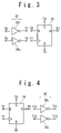
- FIG. 3 is a circuit diagram showing a modification example of the general-purpose logic cell according to the first embodiment of the present invention.
- FIG. 4 is a circuit diagram showing another modification example of the general-purpose logic cell according to the first embodiment of the present invention.
- FIG. 5 is a circuit diagram showing a use example of the general-purpose logic cell according to the first embodiment of the present invention.
- FIG. 6 is a circuit diagram showing another use example of the general-purpose logic cell according to the first embodiment of the present invention.
- FIG. 7 is a circuit diagram showing another use example of the general-purpose logic cell according to the first embodiment of the present invention.
- FIG. 8 is a circuit diagram showing another use example of the general-purpose logic cell according to the first embodiment of the present invention.
- FIG. 9 is a diagram showing the general-purpose logic cell array according to a second embodiment of the present invention.
- FIGS. 10A and 10B are circuit diagrams showing the general-purpose logic cells used in the general-purpose logic cell array according to the second embodiment of the present invention, respectively;
- FIG. 11 is a diagram showing the method of manufacturing an ASIC using the general-purpose logic cell array according to the second embodiment of the present invention.
- FIG. 12 is a block diagram showing the configuration of a designing system used for an ASIC designing.
- MOS transistors formed on a semiconductor substrate for each of basic cells called general-purpose logic cells, and the MOS transistors of each general-purpose logic cell are electrically connected by using a lower wiring line layer of, for example, three layers.
- the general-purpose logic cell array is formed.
- an upper wiring line layer of, for example, two layers is formed on the general-purpose logic cell array as a lower layer in accordance with a logic circuit designed by a user, to connect the above general-purpose logic cells electrically.
- an LSI large-scaled integrated circuit
- ASIC Application Specific IC
- FIG. 2 is a diagram showing the structure of the general-purpose logic cell 1 as a unit module, which is used, as a flip-flop cell according to the first embodiment of the present invention.
- the general-purpose logic cell 1 is composed of a flip-flop 10 , a first inverter set 20 and a second inverter 30 .
- the inverter sets 20 and 30 are used to switch the function of the flip-flop 10 .
- the flip-flop 10 is composed of a D-type flip-flop.
- a clock terminal of the flip-flop 10 is connected with a node T 1
- a data input terminal D is connected with a node T 2
- an output terminal Q is connected with a node T 3
- a set terminal S is connected with a node T 4
- a reset terminal R is connected with a node T 5 .
- the nodes T 1 to T 5 have no connection and are possible to be connected in the upper wiring line layer.
- a MOS transistor with a relatively small size and a small input capacity is used for the transistor of the data input terminal D of the flip-flop 10 .
- a MOS transistor with a smaller size and a smaller input capacity is used for the transistor of a clock terminal.
- a MOS transistor with a relatively large size and a relatively large drive ability is used for the transistor of the output terminal Q of the flip-flop 10 .
- the optimization of the flip-flop is accomplished in this structure. That is, a clock signal supplied to the flip-flop is a signal which always changes.
- the size of the MOS transistor to which the clock signal is supplied is made small to realize low input capacity and low power consumption of the flip-flop.
- the first inverter set 20 is composed of inverters 201 and 202 .
- Each of the inverters 201 and 202 is composed of a plurality of MOS transistors connected by the lower wiring line layer.
- the inverters 201 and 202 are provided for purpose of changing the timing and level of a signal supplied to the flip-flop 10 . Therefore, the large drive ability is not needed for the inverters, and the inverters are formed of MOS transistors with a relatively smaller size and a relatively smaller input capacity, compared with the output transistor of the flip-flop. Thus, the optimization of the inverter is accomplished.
- the input terminal of the inverter 201 is connected with a node T 6 and the output terminal is connected with a node T 7 .
- the input terminal of the inverter 202 is connected with a node T 8 and the output terminal is connected with a node T 9 .
- the nodes T 6 to T 9 have no connection and are possible to be connected in the upper wiring line layer.
- the second inverter set 30 is composed of inverters 301 and 302 .
- Each of the inverters 301 and 302 is composed of a plurality of MOS transistors connected by the lower wiring line layer.
- Each of the inverters 301 and 302 is composed of a plurality of MOS transistors connected in the lower wiring line layer.
- the inverters 301 and 302 are provided for purpose of compensation of a lack of the drive ability of the flip-flop 10 and the change of a signal level. Therefore, the inverters are formed of MOS transistors with a large size and a large drive ability, compared with the output transistor of the flip-flop. Also, the drive abilities of the inverters 301 and 302 may be different from each other. Thus, the optimization of the inverters is accomplished.
- the input terminal of the inverter 301 is connected with a node T 10 and the output terminal is connected with a node T 11 .
- the input terminal of the inverter 302 is connected with a node T 12 and the output terminal is connected with a node T 13 .
- the nodes T 10 to T 13 have no connection and are possible to be connected by the upper wiring line layer.
- the above-mentioned general-purpose logic cell 1 is composed of the flip-flop 10 , the input side inverter set 20 of the two inverters 201 and 202 formed from the MOS transistors of relatively small size and the output side inverter set 30 of the two inverters 301 and 302 formed of MOS transistors of a relatively large size.
- the general-purpose logic cell 1 according to the present invention is not always limited to the above-mentioned structure.
- the general-purpose logic cell 1 may be formed of the flip-flop 10 and the two inverters 201 and 202 formed of the MOS transistors of the relatively small size, as shown in FIG. 3 .
- the general-purpose logic cell 1 may be formed of one flip-flop 10 and two inverters 301 and 302 formed of the MOS transistors of the relatively large size, as shown in FIG. 4 .
- the number of inverters contained in the input side inverter set 20 or output side inverter set 30 is not limited to two, and is optional.
- the other circuits such as a NAND gate and a NOR gate can be used instead of the above inverters 201 , 202 , 301 and 302 .
- the general-purpose logic cell 1 shown in FIG. 2 can be used just as it is as a usual flip-flop.
- the clock signal terminal is the node T 1
- the data input terminal D is the node T 2
- the output terminal Q is the node T 3
- the set terminal S is the node T 4
- the reset terminal R is the node T 5 .
- Each node is connected by a wiring pattern in the upper wiring line layer in accordance with the logic circuit designed by the user.
- FIG. 5 shows a use example when the lack of the drive ability of the flip-flop 10 is compensated.
- the nodes T 3 , T 10 and T 12 are connected to each other by a wiring pattern in the upper wiring line layer and the nodes T 11 and T 13 are connected by a wiring pattern in the upper wiring line layer.
- the flip-flop 10 can be used as a flip-flop, which has its drive ability and drive abilities of the inverters 301 and 302 .
- the clock signal terminal is the node T 1
- the data input terminal D is the node T 2
- the output terminal Q is the node T 11 or T 13
- the set terminal S is the node T 4
- the reset terminal R is the node T 5 .
- Each node is connected by a wiring pattern in the upper wiring line layer in accordance with the logic circuit designed by the user.
- FIG. 6 shows an example when the flip-flop 10 is used as a flip-flop which has an inversion set logic.
- the node T 7 and the node T 4 are connected.
- the flip-flop 10 can be used as a flip-flop, which can be compulsively set, based on a signal of a low (L) level supplied to the node T 6 .
- the clock signal terminal is the node T 1
- the data input terminal D is the node T 2
- the output terminal Q is the node T 3
- the set terminal S is the node T 6
- the reset terminal R is the node T 5 .
- Each node is connected by a wiring pattern in the upper wiring line layer in accordance with the logic circuit designed by the user.
- FIG. 7 shows a use example when the setup time of the flip-flop 10 should be sufficiently secured.
- the node T 7 and the node T 8 are connected and the node T 9 and the node T 1 are connected.
- the signal supplied to the clock signal terminal of the flip-flop 10 is delayed. Therefore, the change of the clock signal to the signal supplied to the data input terminal D is relatively delayed, and the setup time can be secured.
- the clock signal terminal is the node T 6
- the data input terminal D is the node T 2
- the output terminal Q is the node T 3
- the set terminal S is the node T 4
- the reset terminal R is the node T 5 .
- Each node is connected by a wiring pattern in the upper wiring line layer in accordance with the logic circuit designed by the user.
- FIG. 8 shows a use example when the hold time of the flip-flop 10 should be sufficiently secured.
- the node T 6 and the node T 9 are connected and the node T 7 and the node T 2 are connected.
- a signal supplied to the data input terminal D of the flip-flop 10 is delayed. Therefore, a change of the clock signal to a signal supplied to the data input terminal D goes ahead relatively and the fold time can be secured.
- the clock signal terminal is the node T 1
- the data input terminal D is the node T 8
- the output terminal Q is the node T 3
- the set terminal S is the node T 4
- the reset terminal R is the node T 5 .
- Each node is connected by a wiring pattern in the upper wiring line layer in accordance with the logic circuit designed by the user.
- the general-purpose logic cell it is possible to switch the plurality of functions in one general-purpose logic cell 1 . Also, in case that the logic circuit designed by the user is achieved by the upper wiring line layer formed on the lower layer, an defect can be corrected even if the defect occurs in the process after the arrangement process. Therefore, it is possible to shorten a development term of the semiconductor device and to reduce the development cost. Also, even if the function of one general-purpose logic cell 1 is switched between the flip-flop functions, the wiring line length is short so that efficiency lowering can be prevented.
- FIG. 9 is a diagram showing the structure of the general-purpose logic cell array containing the general-purpose logic cells 1 .
- the general-purpose logic cell array is composed of three kinds of general-purpose logic cells such as a general-purpose logic cell CELL-A, a general-purpose logic cell CELL-B and a general-purpose logic cell CELL-C.
- Each of the general-purpose logic cell CELL-A, the general-purpose logic cell CELL-B and the general-purpose logic cell CELL-C is arranged in one line in Y-axis direction, and they are arranged circularly in the order of the general-purpose logic cell CELL-A, the general-purpose logic cell CELL-B and the general-purpose logic cell CELL-C in the X-axis direction.
- the ratio may be optionally set.
- the general-purpose logic cell CELL-A is composed of a selector 31 , as shown in FIG. 10A .
- a first input terminal 0 of the selector 31 is connected with a node T 20
- a second input terminal 1 is connected with a node T 21
- a selection control terminal S is connected with a node T 22
- an output terminal is connected with a node T 23 .
- the selector 31 is formed by connecting a plurality of MOS transistors by the lower wiring line layer.
- the nodes T 20 to T 23 are connected by a wiring pattern in the upper wiring line layer in accordance with the logic circuit designed by the user.
- a MOS transistor with a relatively small size and a small input capacity is used for the transistors of the first input terminal 0 , second input terminal 1 and selection input terminal S of the selector 31 .
- a MOS transistor with a relatively large size and a relatively large drive ability is used for the transistor of the output terminal. Thus, the optimization of the selector 31 is accomplished.
- a selector disclosed in Japanese Patent Application No. 2000-349627 may be used as the general-purpose logic cell CELL-A.
- the selector is formed such that inverters receive a signal supplied to the first input terminal 0 and a signal supplied to the second input terminal 1 and the outputs of the inverters are drawn out as signals at middle nodes. If the selector is used, a gate circuit operating at a high speed can be formed of a few numbers of the wiring lines.
- the general logic cell CELL-B is formed from the general-purpose logic cell 1 containing the flip-flop shown in FIG. 2 .
- the general-purpose logic cell CELL-C is composed of an inverter 32 as shown in FIG. 10B .
- An input terminal of the inverter 32 is connected with a node T 24 and an output terminal is connected with a node T 25 .
- the inverter 32 is formed by connecting a plurality of MOS transistors by the lower wiring line layer.
- the nodes T 24 and T 25 are connected by a wiring pattern in the upper wiring line layer in accordance with the logic circuit designed by the user.
- a MOS transistor with a relatively small size and a relatively small input capacity is used for the MOS transistor of the input terminal of the inverter 32 .
- a MOS transistor with a large size and a large drive ability is used for the transistor of the output terminal.
- the designing system is composed of a processor 102 , an input unit 104 , a display unit 106 , a general-purpose logic cell data storage 108 and a storage unit 110 and a recording medium 112 .
- An arrangement program and a wiring line program are loaded into the storage unit 110 from the recording medium 112 .
- the storage unit 108 stores data of the general-purpose logic cell array, i.e., data of a layout and attributes of the MOS transistors in each of the logic cells, and a layout of connections of the MOS transistors in the lower wiring line layer.
- the processor 102 reads out the general-purpose logic cell array data from the storage unit 108 and provides it to a user automatically via the Internet or manually. When receiving data of a desired logic circuit from the user automatically via the Internet or manually, the processor 102 starts the arrangement program 110 - 1 and the wiring line program 110 - 2 to produce a layout of wiring lines for the upper wiring line layer.
- MOS transistors are formed on a semiconductor substrate, and are electrically connected by a lower wiring line layer of three layers.
- a lower layer is formed in which three kinds of the general-purpose logic cells such as the general-purpose logic cell CELL-A, the general-purpose logic cell CELL-B and the general-purpose logic cell CELL-C are formed in an array.
- the number of layers in the lower wiring line layer is not limited to three.
- the lower wiring line layer may be formed of the optional number of layers in accordance with the structure of each the general-purpose logic cell.
- an arrangement process of the general-purpose logic cells is carried out, by using an arrangement program 110 - 1 .
- regions for one selector, one flip-flop and two inverters are secured adjacently to each other in an unused region of the general-purpose logic cell array.
- one flip-flop and two inverters are arranged for the function block FB 1 , as shown in FIG. 9 by the slanted lines.
- the general-purpose logic cells are secured and arranged to realize another function block FB 2 and another function block FB 3 contained in the logic circuit shown from the user.
- the function block FB 2 two flip-flops are secured and arranged
- the function block FB 3 three selectors and two flip-flops are secured and arranged.
- a wiring process is carried out by using a wiring line program 110 - 2 . That is, a wiring pattern is produced to connect the nodes of the respective general-purpose logic cells, as shown in FIG. 11 by the broken lines. Using a lithography mask on which the produced wiring pattern is baked, the semiconductor manufacturing process is carried out to form the upper wiring line layer on the semiconductor substrate in which the lower layer has the 3-layer lower wiring line layer. Thus, the semiconductor chip is completed in which the logic circuit shown by the user is formed on the general-purpose logic cell array.
- the inverters 32 of the general-purpose logic cell CELL-C are used as the inverter in the above-mentioned example.
- the inverters 301 and 302 provided in the general-purpose logic cell 1 as shown in FIG. 5 may be used. In this case, it is possible to shorten a wiring length in accordance with the structure.
- the above-mentioned arrangement process and wiring process are carried out to realize the logic circuit shown from the user, and then the wiring pattern of the upper wiring line layer is designed.
- the design of ASIC completes.
- the semiconductor manufacturing process is carried out in which the upper wiring line layer is formed on the semiconductor substrate as the lower layer with the 3-layer lower wiring line layer.
- the semiconductor chip is completed in which the logic circuit shown by the user is formed.
- the ASIC which uses the general-purpose logic cell array according to the second embodiment of the present invention is provided to the user in the following ways.
- a semiconductor maker shows information of the semiconductor substrate in which the 3-layer lower wiring line layer is formed.
- the user designs a desired logic circuit based on the shown information and requests the manufacturing of semiconductor chips to the semiconductor maker to realize the desired logic circuit.
- the semiconductor maker designs the upper wiring line pattern of two layers automatically based on the logic circuit design received from the user.
- the semiconductor maker manufactures semiconductor chips as mentioned above, and provides them for the user.
- the semiconductor maker is sufficient to connect between the nodes of the general-purpose logic cells by the upper wiring line layer which is formed on the semiconductor substrate as the lower layer with the 3-layer lower wiring line layer. Therefore, it is not necessary to carry out all connections in the upper wiring line layer like a cell array of the gate array type. As a result, wiring line resource neck can be eliminated.
- the general-purpose logic cell array according to the second embodiment of the present invention is composed of a plurality of kinds of the general-purpose logic cells such as the selector, the flip-flop and the inverter.
- the general-purpose logic cell is optimized. Therefore, the optimization can be automatically carried out from the nature of the logic circuit shown by the user, e.g., from the viewpoints of which of a combinational circuit, a sequential circuit and a drive circuit is used the most. In this way, the power consumption, the input capacity, and the drive ability can be optimized by combining a plurality of general-purpose logic cell arrays appropriately.
- the drive ability is lack, even if an inverter is supposed to be optimized in the drive circuit having only the inverter. In such a case, in the present invention, the drive ability can be improved by connecting two or more inverters in parallel, as shown in FIG. 11 . Therefore, the drive ability can be simply optimized.
- the plurality of general-purpose logic cells are composed of a 2-input multiplexer, a flip-flop (the general-purpose logic cell according to the first embodiment) and an inverter.
- the general-purpose logic cells are not limited to them, and the other various logic circuits may be used as the general-purpose logic cell.
- the general-purpose logic cell array is composed of one or more kinds of the general-purpose logic cells.
- a semiconductor circuit such as a CPU, a memory, and analog circuits such as a PLL circuit and an analog-to-digital converter, other than the digital general-purpose logic cells, in a part of the area of the general-purpose logic cell array.
- the ASIC can be manufactured on one semiconductor chip to have very many functions.
- the general-purpose logic cell for developing a semiconductor device in which a logic circuit designed by a user is incorporated, can be provided in a short time and in a low cost.
- the general-purpose logic cell array using the general-purpose logic cells, and the ASIC using the general-purpose logic cell array can be provided.
Abstract
Description
Claims (19)
Applications Claiming Priority (2)
| Application Number | Priority Date | Filing Date | Title |
|---|---|---|---|
| JP2002144354A JP2003338750A (en) | 2002-05-20 | 2002-05-20 | General-purpose logic cell, general-purose logic cell array using same, and asic using the general-purpose logic cell array |
| JP144354/2002 | 2002-05-20 |
Publications (2)
| Publication Number | Publication Date |
|---|---|
| US20030214323A1 US20030214323A1 (en) | 2003-11-20 |
| US7161382B2 true US7161382B2 (en) | 2007-01-09 |
Family
ID=29397735
Family Applications (1)
| Application Number | Title | Priority Date | Filing Date |
|---|---|---|---|
| US10/438,012 Expired - Lifetime US7161382B2 (en) | 2002-05-20 | 2003-05-15 | General-purpose logic cell, general-purpose logic cell array using the same, and ASIC using general-purpose logic cell array |
Country Status (3)
| Country | Link |
|---|---|
| US (1) | US7161382B2 (en) |
| EP (1) | EP1365513A3 (en) |
| JP (1) | JP2003338750A (en) |
Families Citing this family (1)
| Publication number | Priority date | Publication date | Assignee | Title |
|---|---|---|---|---|
| US10762664B2 (en) * | 2017-12-29 | 2020-09-01 | Intel Corporation | Multi-camera processor with feature matching |
Citations (32)
| Publication number | Priority date | Publication date | Assignee | Title |
|---|---|---|---|---|
| JPH01204445A (en) | 1988-02-09 | 1989-08-17 | Nec Corp | Semiconductor integrated circuit |
| EP0343968A2 (en) | 1988-05-25 | 1989-11-29 | Fujitsu Limited | Programmable logic device |
| JPH0268951A (en) | 1988-09-03 | 1990-03-08 | Nec Corp | Master slice system semiconductor integrated circuit |
| US4910417A (en) | 1986-09-19 | 1990-03-20 | Actel Corporation | Universal logic module comprising multiplexers |
| JPH02222217A (en) | 1989-02-22 | 1990-09-05 | Toshiba Corp | Programmable logic circuit |
| EP0426283A2 (en) | 1989-10-31 | 1991-05-08 | STMicroelectronics, Inc. | Input row drivers for programmable logic devices |
| WO1991007015A1 (en) | 1989-10-25 | 1991-05-16 | Concurrent Logic, Inc. | Programmable logic cell and array |
| US5055718A (en) | 1990-05-11 | 1991-10-08 | Actel Corporation | Logic module with configurable combinational and sequential blocks |
| JPH05167048A (en) | 1991-12-13 | 1993-07-02 | Kawasaki Steel Corp | Gate array |
| US5225718A (en) | 1989-05-29 | 1993-07-06 | Kabushiki Kaisha Toshiba | Standard-cell type semiconductor logic lsi with logical amplitude enhancer |
| US5243208A (en) | 1987-05-27 | 1993-09-07 | Hitachi, Ltd. | Semiconductor integrated circuit device having a gate array with a ram and by-pass signal lines which interconnect a logic section and I/O unit circuit of the gate array |
| US5457410A (en) | 1993-08-03 | 1995-10-10 | Btr, Inc. | Architecture and interconnect scheme for programmable logic circuits |
| JPH09116124A (en) | 1995-08-18 | 1997-05-02 | Chip Express Israel Ltd | Cell forming part of custom-made logic array |
| EP0776093A2 (en) | 1993-06-18 | 1997-05-28 | Pilkington Micro-Electronics Limited | Configurable logic array |
| JPH09148916A (en) | 1995-11-24 | 1997-06-06 | Nec Corp | Semiconductor integrated circuit |
| TW308696B (en) | 1995-12-29 | 1997-06-21 | Samsung Electronics Co Ltd | Semiconductor memory device having dual banks simultaneously operating by single row address strobe signal |
| US5646558A (en) | 1995-09-27 | 1997-07-08 | Intel Corporation | Plurality of distinct multiplexers that operate as a single multiplexer |
| JPH10223902A (en) | 1997-02-03 | 1998-08-21 | Nec Corp | Semiconductor integrated circuit device |
| US5898636A (en) | 1993-06-21 | 1999-04-27 | Hitachi, Ltd. | Semiconductor integrated circuit device with interleaved memory and logic blocks |
| US5920089A (en) | 1996-06-28 | 1999-07-06 | Kabushiki Kaisha Toshiba | Multi-power supply integrated circuit and system employing the same |
| US5955912A (en) | 1995-10-25 | 1999-09-21 | Texas Instruments Incorporated | Multiplexer circuits |
| JPH11265998A (en) | 1998-01-13 | 1999-09-28 | Mitsubishi Electric Corp | Semiconductor device and its manufacture |
| US6014038A (en) | 1997-03-21 | 2000-01-11 | Lightspeed Semiconductor Corporation | Function block architecture for gate array |
| US6020772A (en) | 1998-02-05 | 2000-02-01 | International Business Machines Corporation | Flash output LSSD latch |
| US6278148B1 (en) | 1997-03-19 | 2001-08-21 | Hitachi, Ltd. | Semiconductor device having a shielding conductor |
| US6300793B1 (en) * | 1995-05-03 | 2001-10-09 | Btr, Inc. | Scalable multiple level tab oriented interconnect architecture |
| US6356118B1 (en) | 1999-04-16 | 2002-03-12 | Hitachi Ltd | Semiconductor integrated circuit device |
| US20020047727A1 (en) | 2000-10-19 | 2002-04-25 | Masaharu Mizuno | General-purpose logic module and cell using the same |
| US6396087B1 (en) | 1999-11-18 | 2002-05-28 | Kabushiki Kaisha Toshiba | Semiconductor integrated circuit |
| US6580289B2 (en) * | 2001-06-08 | 2003-06-17 | Viasic, Inc. | Cell architecture to reduce customization in a semiconductor device |
| US20030173642A1 (en) * | 2002-03-13 | 2003-09-18 | Nec Electronics Corporation | General-purpose logic array and ASIC using the same |
| US20030234666A1 (en) * | 2002-06-19 | 2003-12-25 | Cox William D. | Logic array devices having complex macro-cell architecture and methods facilitating use of same |
-
2002
- 2002-05-20 JP JP2002144354A patent/JP2003338750A/en active Pending
-
2003
- 2003-05-15 EP EP03010939A patent/EP1365513A3/en not_active Withdrawn
- 2003-05-15 US US10/438,012 patent/US7161382B2/en not_active Expired - Lifetime
Patent Citations (36)
| Publication number | Priority date | Publication date | Assignee | Title |
|---|---|---|---|---|
| US4910417A (en) | 1986-09-19 | 1990-03-20 | Actel Corporation | Universal logic module comprising multiplexers |
| US5243208A (en) | 1987-05-27 | 1993-09-07 | Hitachi, Ltd. | Semiconductor integrated circuit device having a gate array with a ram and by-pass signal lines which interconnect a logic section and I/O unit circuit of the gate array |
| JPH01204445A (en) | 1988-02-09 | 1989-08-17 | Nec Corp | Semiconductor integrated circuit |
| EP0343968A2 (en) | 1988-05-25 | 1989-11-29 | Fujitsu Limited | Programmable logic device |
| JPH0268951A (en) | 1988-09-03 | 1990-03-08 | Nec Corp | Master slice system semiconductor integrated circuit |
| JPH02222217A (en) | 1989-02-22 | 1990-09-05 | Toshiba Corp | Programmable logic circuit |
| US5225718A (en) | 1989-05-29 | 1993-07-06 | Kabushiki Kaisha Toshiba | Standard-cell type semiconductor logic lsi with logical amplitude enhancer |
| WO1991007015A1 (en) | 1989-10-25 | 1991-05-16 | Concurrent Logic, Inc. | Programmable logic cell and array |
| EP0426283A2 (en) | 1989-10-31 | 1991-05-08 | STMicroelectronics, Inc. | Input row drivers for programmable logic devices |
| US5055718A (en) | 1990-05-11 | 1991-10-08 | Actel Corporation | Logic module with configurable combinational and sequential blocks |
| JPH05167048A (en) | 1991-12-13 | 1993-07-02 | Kawasaki Steel Corp | Gate array |
| EP0776093A2 (en) | 1993-06-18 | 1997-05-28 | Pilkington Micro-Electronics Limited | Configurable logic array |
| US5898636A (en) | 1993-06-21 | 1999-04-27 | Hitachi, Ltd. | Semiconductor integrated circuit device with interleaved memory and logic blocks |
| US5457410A (en) | 1993-08-03 | 1995-10-10 | Btr, Inc. | Architecture and interconnect scheme for programmable logic circuits |
| US6300793B1 (en) * | 1995-05-03 | 2001-10-09 | Btr, Inc. | Scalable multiple level tab oriented interconnect architecture |
| JPH09116124A (en) | 1995-08-18 | 1997-05-02 | Chip Express Israel Ltd | Cell forming part of custom-made logic array |
| US5684412A (en) | 1995-08-18 | 1997-11-04 | Chip Express (Israel) Ltd. | Cell forming part of a customizable logic array |
| US5646558A (en) | 1995-09-27 | 1997-07-08 | Intel Corporation | Plurality of distinct multiplexers that operate as a single multiplexer |
| US5955912A (en) | 1995-10-25 | 1999-09-21 | Texas Instruments Incorporated | Multiplexer circuits |
| JPH09148916A (en) | 1995-11-24 | 1997-06-06 | Nec Corp | Semiconductor integrated circuit |
| TW308696B (en) | 1995-12-29 | 1997-06-21 | Samsung Electronics Co Ltd | Semiconductor memory device having dual banks simultaneously operating by single row address strobe signal |
| US5920089A (en) | 1996-06-28 | 1999-07-06 | Kabushiki Kaisha Toshiba | Multi-power supply integrated circuit and system employing the same |
| JPH10223902A (en) | 1997-02-03 | 1998-08-21 | Nec Corp | Semiconductor integrated circuit device |
| US6278148B1 (en) | 1997-03-19 | 2001-08-21 | Hitachi, Ltd. | Semiconductor device having a shielding conductor |
| US6014038A (en) | 1997-03-21 | 2000-01-11 | Lightspeed Semiconductor Corporation | Function block architecture for gate array |
| JPH11265998A (en) | 1998-01-13 | 1999-09-28 | Mitsubishi Electric Corp | Semiconductor device and its manufacture |
| US6020772A (en) | 1998-02-05 | 2000-02-01 | International Business Machines Corporation | Flash output LSSD latch |
| US6356118B1 (en) | 1999-04-16 | 2002-03-12 | Hitachi Ltd | Semiconductor integrated circuit device |
| US6396087B1 (en) | 1999-11-18 | 2002-05-28 | Kabushiki Kaisha Toshiba | Semiconductor integrated circuit |
| US20020047727A1 (en) | 2000-10-19 | 2002-04-25 | Masaharu Mizuno | General-purpose logic module and cell using the same |
| US20030201798A1 (en) | 2000-10-19 | 2003-10-30 | Nec Electronics Corporation | General-purpose logic module and cell using the same |
| US6674307B2 (en) | 2000-10-19 | 2004-01-06 | Nec Electronics Corporation | General-purpose logic module and cell using the same |
| US6580289B2 (en) * | 2001-06-08 | 2003-06-17 | Viasic, Inc. | Cell architecture to reduce customization in a semiconductor device |
| US20030173642A1 (en) * | 2002-03-13 | 2003-09-18 | Nec Electronics Corporation | General-purpose logic array and ASIC using the same |
| US20030234666A1 (en) * | 2002-06-19 | 2003-12-25 | Cox William D. | Logic array devices having complex macro-cell architecture and methods facilitating use of same |
| US6873185B2 (en) * | 2002-06-19 | 2005-03-29 | Viasic, Inc. | Logic array devices having complex macro-cell architecture and methods facilitating use of same |
Non-Patent Citations (1)
| Title |
|---|
| U.S. Appl. No. 10/437,391 (projected publication date: Nov. 20, 2003). |
Also Published As
| Publication number | Publication date |
|---|---|
| JP2003338750A (en) | 2003-11-28 |
| US20030214323A1 (en) | 2003-11-20 |
| EP1365513A3 (en) | 2006-10-18 |
| EP1365513A2 (en) | 2003-11-26 |
Similar Documents
| Publication | Publication Date | Title |
|---|---|---|
| US6938226B2 (en) | 7-tracks standard cell library | |
| KR101690170B1 (en) | Custom integrated circuit | |
| US6823499B1 (en) | Method for designing application specific integrated circuit structure | |
| US7412679B2 (en) | Semiconductor integrated circuit and semiconductor integrated circuit manufacturing method | |
| US7162707B2 (en) | Scan path timing optimizing apparatus determining connection order of scan path circuits to realize optimum signal timings | |
| US4728823A (en) | Logic circuit testable as an inverter pair and operable as a flip-flop | |
| US6536030B1 (en) | Macroblock for use in layout design of semiconductor integrated circuit, storage medium for storing intellectual property including information on the macroblock, and layout design method using the macroblock | |
| US7161382B2 (en) | General-purpose logic cell, general-purpose logic cell array using the same, and ASIC using general-purpose logic cell array | |
| JP2004198269A (en) | Semiconductor integrated circuit device | |
| KR100303675B1 (en) | Semiconductor device and method of fabricating the same | |
| US6992504B2 (en) | General-purpose logic array and ASIC using the same | |
| JP3891813B2 (en) | Hierarchical design method for integrated logic circuits | |
| JP2005252143A (en) | Semiconductor integrated circuit | |
| US6501106B1 (en) | Semiconductor integrated circuit device and method of producing the same | |
| JP3546582B2 (en) | Semiconductor device | |
| US7185307B2 (en) | Method of fabricating and integrated circuit through utilizing metal layers to program randomly positioned basic units | |
| JP4156864B2 (en) | Semiconductor device and manufacturing method thereof | |
| JPH11265998A (en) | Semiconductor device and its manufacture | |
| JPH1093422A (en) | Programmable logic circuit | |
| JPH10173054A (en) | Designing method for low power consumption of semiconductor integrated circuit | |
| JPWO2009047840A1 (en) | Semiconductor integrated circuit device | |
| JPH10125085A (en) | Semiconductor integrated circuit | |
| JP2005259781A (en) | Method of manufacturing semiconductor integrated circuit | |
| JPH09148442A (en) | Method for designing integrated circuit | |
| JPH05326843A (en) | Semiconductor integrated circuit device |
Legal Events
| Date | Code | Title | Description |
|---|---|---|---|
| AS | Assignment |
Owner name: NEC ELECTRONICS CORPORATION, JAPAN Free format text: ASSIGNMENT OF ASSIGNORS INTEREST;ASSIGNORS:MIZUNO, MASAHARU;FUJII, TOORU;REEL/FRAME:014080/0473 Effective date: 20030507 |
|
| FEPP | Fee payment procedure |
Free format text: PAYOR NUMBER ASSIGNED (ORIGINAL EVENT CODE: ASPN); ENTITY STATUS OF PATENT OWNER: LARGE ENTITY |
|
| STCF | Information on status: patent grant |
Free format text: PATENTED CASE |
|
| FPAY | Fee payment |
Year of fee payment: 4 |
|
| AS | Assignment |
Owner name: RENESAS ELECTRONICS CORPORATION, JAPAN Free format text: CHANGE OF NAME;ASSIGNOR:NEC ELECTRONICS CORPORATION;REEL/FRAME:025525/0154 Effective date: 20100401 |
|
| FPAY | Fee payment |
Year of fee payment: 8 |
|
| AS | Assignment |
Owner name: RENESAS ELECTRONICS CORPORATION, JAPAN Free format text: CHANGE OF ADDRESS;ASSIGNOR:RENESAS ELECTRONICS CORPORATION;REEL/FRAME:044928/0001 Effective date: 20150806 |
|
| MAFP | Maintenance fee payment |
Free format text: PAYMENT OF MAINTENANCE FEE, 12TH YEAR, LARGE ENTITY (ORIGINAL EVENT CODE: M1553) Year of fee payment: 12 |