US7162410B1 - In-circuit emulator with gatekeeper for watchdog timer - Google Patents
In-circuit emulator with gatekeeper for watchdog timer Download PDFInfo
- Publication number
- US7162410B1 US7162410B1 US10/004,039 US403901A US7162410B1 US 7162410 B1 US7162410 B1 US 7162410B1 US 403901 A US403901 A US 403901A US 7162410 B1 US7162410 B1 US 7162410B1
- Authority
- US
- United States
- Prior art keywords
- microcontroller
- gatekeeper
- clock
- virtual
- data
- Prior art date
- Legal status (The legal status is an assumption and is not a legal conclusion. Google has not performed a legal analysis and makes no representation as to the accuracy of the status listed.)
- Expired - Lifetime, expires
Links
- 238000000034 method Methods 0.000 claims description 34
- 230000015654 memory Effects 0.000 claims description 32
- 230000006854 communication Effects 0.000 claims description 25
- 238000004891 communication Methods 0.000 claims description 24
- 238000012545 processing Methods 0.000 claims description 12
- 230000006870 function Effects 0.000 description 33
- 238000012546 transfer Methods 0.000 description 26
- 230000008569 process Effects 0.000 description 15
- 238000013461 design Methods 0.000 description 13
- 239000013598 vector Substances 0.000 description 11
- 238000004519 manufacturing process Methods 0.000 description 10
- 238000012360 testing method Methods 0.000 description 9
- 238000011161 development Methods 0.000 description 8
- 230000018109 developmental process Effects 0.000 description 8
- 238000010586 diagram Methods 0.000 description 7
- 230000008901 benefit Effects 0.000 description 6
- 230000004044 response Effects 0.000 description 6
- 239000000523 sample Substances 0.000 description 6
- 238000004458 analytical method Methods 0.000 description 5
- 230000007246 mechanism Effects 0.000 description 5
- 230000002457 bidirectional effect Effects 0.000 description 4
- 230000007704 transition Effects 0.000 description 4
- 241000218691 Cupressaceae Species 0.000 description 3
- 230000009471 action Effects 0.000 description 3
- 230000005540 biological transmission Effects 0.000 description 3
- 230000000694 effects Effects 0.000 description 3
- 230000004048 modification Effects 0.000 description 3
- 238000012986 modification Methods 0.000 description 3
- 230000007175 bidirectional communication Effects 0.000 description 2
- 230000003287 optical effect Effects 0.000 description 2
- 102100029272 5-demethoxyubiquinone hydroxylase, mitochondrial Human genes 0.000 description 1
- 101000770593 Homo sapiens 5-demethoxyubiquinone hydroxylase, mitochondrial Proteins 0.000 description 1
- 230000006399 behavior Effects 0.000 description 1
- 230000015572 biosynthetic process Effects 0.000 description 1
- 230000008859 change Effects 0.000 description 1
- 239000013065 commercial product Substances 0.000 description 1
- 238000004590 computer program Methods 0.000 description 1
- 230000007547 defect Effects 0.000 description 1
- 238000003745 diagnosis Methods 0.000 description 1
- 238000005516 engineering process Methods 0.000 description 1
- 238000009432 framing Methods 0.000 description 1
- 230000010354 integration Effects 0.000 description 1
- 239000003550 marker Substances 0.000 description 1
- 239000000463 material Substances 0.000 description 1
- 230000006386 memory function Effects 0.000 description 1
- 230000008520 organization Effects 0.000 description 1
- 239000000047 product Substances 0.000 description 1
- 230000008672 reprogramming Effects 0.000 description 1
- 230000000630 rising effect Effects 0.000 description 1
- 238000004088 simulation Methods 0.000 description 1
- 239000000126 substance Substances 0.000 description 1
- 238000003786 synthesis reaction Methods 0.000 description 1
- 230000036962 time dependent Effects 0.000 description 1
- 230000003245 working effect Effects 0.000 description 1
Images


Classifications
-
- G—PHYSICS
- G06—COMPUTING; CALCULATING OR COUNTING
- G06F—ELECTRIC DIGITAL DATA PROCESSING
- G06F11/00—Error detection; Error correction; Monitoring
- G06F11/36—Preventing errors by testing or debugging software
- G06F11/362—Software debugging
- G06F11/3648—Software debugging using additional hardware
- G06F11/3652—Software debugging using additional hardware in-circuit-emulation [ICE] arrangements
-
- G—PHYSICS
- G06—COMPUTING; CALCULATING OR COUNTING
- G06F—ELECTRIC DIGITAL DATA PROCESSING
- G06F11/00—Error detection; Error correction; Monitoring
- G06F11/36—Preventing errors by testing or debugging software
- G06F11/362—Software debugging
- G06F11/3648—Software debugging using additional hardware
- G06F11/3656—Software debugging using additional hardware using a specific debug interface
Definitions
- This invention relates generally to the field of In-Circuit Emulation. More particularly, this invention in certain embodiments relates to methods and apparatus for providing for watchdog timer functions using a gatekeeper in an In-Circuit Emulation system.
- In-circuit emulation has been used by software and hardware developers for a number of years as a development tool to emulate the operation of complex circuit building blocks and permit diagnosis and debugging of hardware and software.
- Such in-circuit emulation is most commonly used currently to analyze and debug the behavior of complex devices such as microcontrollers and microprocessors that have internal structures that are far too complex to readily model using computer simulation software alone.
- FIG. 1 illustrates an exemplary conventional in-circuit emulation arrangement 100 used to model, analyze and debug the operation of a microcontroller device.
- a host computer e.g., a personal computer
- a debug logic block 120 which is further connected to a special version of the microcontroller device that has been developed specially for use in emulation. Operational instructions are loaded from the host computer 110 through the debug logic 120 to the special version of the microcontroller 130 .
- the debug logic 120 monitors operation of the microcontroller 130 as the instructions are executed.
- this operation may be monitored while the special version of the microcontroller 130 is interconnected with the circuitry that is intended to interface a production version of the microcontroller in the finished product under development. Such interconnection may be via simulation within host computer 110 or as actual circuitry or some combination thereof. As the circuit is stepped through its operation, the debug logic gathers information about the state of various components of the microcontroller 130 during operation and feeds that information back to the host computer 110 for analysis.
- various trace information such as time stamps, register values, data memory content, etc. may be logged in the host computer 110 for analysis and debugging by the designer. Additionally, it is generally the case that various break points can be defined by the designer that cause the program to halt execution at various points in the operation to permit detailed analysis. Other debugging tools may also be provided to enable the user to debug the operation of the circuit.
- In-circuit emulation systems such as 100 have a number of disadvantages and limitations.
- the microcontroller 130 might have been simply the production version of the microcontroller itself with no special debugging features.
- the information that can be gathered by the ICE system 100 is limited to that which is available at the pinouts of the microcontroller 130 (or which can be extracted from the microcontroller using clever programming or special coding supported by the processor).
- Enhancements to such early systems provided the microcontroller or other processor with an array of built-in debugging tools that use standard pins on the part and built-in instructions that facilitated in-circuit emulation.
- the emulation tools are integrated into the part and thus become a design constraint for developing and improving the part.
- support for the debugging instruction code and the like can increase the cost and complexity of the circuit.
- a bond-out version of the microcontroller is a version of the production microcontroller that has been designed with special wirebonding pads on the chip that are not normally connected in the production wirebonding.
- the bond-out version connects these pads to pins on the microcontroller package to permit access to otherwise inaccessible points of the circuit to facilitate debugging.
- This technique is in common use, but has the disadvantage of imposing significant limitations on the circuit layout to permit space and circuitry associated with the special wirebonding pads. Additionally, it is usually the case that substantial interface circuitry and other special circuitry to facilitate the debugging and bond-out has to be added to the circuit. This increases the complexity, size, power consumption and potentially reduces the yield of the production part.
- a third technique one that is used in the PentiumTM and Pentium ProTM series of microprocessors available from Intel Corporation, provides a special “probe mode” of operation of the processor.
- a number of internal signals are routed to a “debug port” for use by the in-circuit emulation system.
- This debug port is used to permit the in-circuit emulation system to communicate with the processors at all times and, when placed in probe mode, to read otherwise inaccessible probe points within the processor.
- providing such a probe mode requires significant design resources to design in all such probe and debug functions and associated instruction code support into the standard processor. This, of course, increases development cost, chip complexity and chip size. Moreover, such facilities become a part of the processor design which must be carried through and updated as required as enhancements to the original design are developed.
- the present invention relates generally to handling watchdog timer events in an ICE system. Objects, advantages and features of the invention will become apparent to those skilled in the art upon consideration of the following detailed description of the invention.
- a watchdog timer control uses a gatekeeper in an In-Circuit Emulation system.
- the In-Circuit Emulation system has a microcontroller operating in lock-step synchronization with a virtual microcontroller.
- the gatekeeper When a watchdog event occurs, the gatekeeper, forming a part of the virtual microcontroller, crowbars the reset line of the virtual microcontroller as well as the real microcontroller. This freezes the state of the virtual microcontroller so that debug operations can be carried out.
- the gatekeeper operates with its own gatekeeper clock independent of the microcontroller clock. When a watchdog event occurs, the gatekeeper clock is rerouted to the virtual microcontroller to facilitate debug operations of the virtual microcontroller. This advantageously permits the host computer to query the registers and memory of the virtual microcontroller after a watchdog event has occurred.
- An In-Circuit Emulation system consistent with certain embodiments of the present invention has a microcontroller having a microcontroller clock and a virtual microcontroller running in lock-step synchronization with the microcontroller.
- a host computer runs In-Circuit Emulation debug software, the host computer being in communication with the virtual microcontroller.
- a gatekeeper circuit coupled to the virtual microcontroller and the microcontroller, the gatekeeper circuit detecting when a watchdog timer expires in the microcontroller and notifying the host computer that the watchdog event has occurred.
- a method of processing a watchdog timer event using a gatekeeper circuit in a manner consistent with certain embodiment of the present invention includes determining that a watchdog timer event has occurred in a microcontroller, the microcontroller running in lock-step synchronization with a virtual microcontroller; asserting a reset in the microcontroller and by holding the reset line of the microcontroller in an asserted state; providing a gatekeeper clock signal to the virtual microcontroller; notifying a host computer running In-Circuit Emulation software that a watchdog timer event has occurred; and permitting the host computer to query memory locations and registers of the virtual microcontroller.
- a method consistent with certain embodiments of the present invention of processing a watchdog timer event using a gatekeeper circuit includes determining that a watchdog timer event has occurred in a microcontroller, the microcontroller running in lock-step synchronization with a virtual microcontroller; asserting a reset in the microcontroller and by holding the reset line of the microcontroller in an asserted state; disabling a microcontroller clock signal from the virtual microcontroller and replacing the microcontroller clock signal with a gatekeeper clock signal to the virtual microcontroller; and notifying a host computer running In-Circuit Emulation software that a watchdog timer event has occurred.
- FIG. 1 is a block diagram of a conventional In-Circuit Emulation system.
- FIG. 2 is a block diagram of an exemplary In-Circuit Emulation system consistent with certain microcontroller embodiments of the present invention.
- FIG. 3 is an illustration of the operational phases of an In-Circuit Emulation system consistent with an embodiment of the present invention.
- FIG. 4 is an illustration of the operational phases of an In-Circuit Emulation system consistent with an embodiment of the present invention viewed from a virtual microcontroller perspective.
- FIG. 5 is a timing diagram useful in understanding an exemplary data and control phase of operation of certain embodiments of the present invention.
- FIG. 6 is a block diagram isolating the host to FPGA interface consistent with an embodiment of the present invention
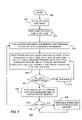
- FIG. 7 is a flow chart describing the operation of the host to FPGA interface in an embodiment consistent with the present invention.
- FIG. 8 is a block diagram illustrating the gatekeeper function of an ICE system consistent with certain embodiments of the present invention.
- FIG. 9 is a flow chart of a halt process used in certain embodiments consistent with the present invention.
- FIG. 10 is a flow chart of a watchdog process used in certain embodiments consistent with the present invention.
- these quantities take the form of electrical or magnetic signals capable of being stored, transferred, combined, compared, and otherwise manipulated in a computer system. It has proven convenient at times, principally for reasons of common usage, to refer to these signals as bits, values, elements, symbols, characters, terms, numbers, or the like.
- a commercial ICE system utilizing the present invention is available from Cypress Micro Systems, Inc., for the CY8C25xxx/26xxx series of microcontrollers. Detailed information regarding this commercial product is available from Cypress Micro Systems, Inc., 22027 17th Avenue SE, Suite 201, Bothell, Wash. 98021, in the form of version 1.11 of “PSoC Designer: Integrated Development Environment User Guide”, which is hereby incorporated by reference. While the present invention is described in terms of an ICE system for the above exemplary microcontroller device, the invention is equally applicable to other complex circuitry including microprocessors and other circuitry that is suitable for analysis and debugging using in-circuit emulation. Moreover, the invention is not limited to the exact implementation details of the exemplary embodiment used herein for illustrative purposes.
- a Host computer 210 e.g., a personal computer based on a PentiumTM class microprocessor
- a standard PC interface 214 such as a parallel printer port connection, a universal serial port (USB) connection, etc.
- the host computer 210 generally operates to run an ICE computer program to control the emulation process and further operates in the capacity of a logic analyzer to permit a user to view information provided from the base station 218 for use in analyzing and debugging a system under test or development.
- the base station 218 is based upon a general purpose programmable hardware device such as a gate array configured to function as a functionally equivalent “virtual microcontroller” 220 (or other device under test (DUT)). This is accomplished using an associated integral memory 222 which stores program instructions, data, trace information and other associated information.
- the base station is configured as an emulator of the internal microprocessor portion of the microcontroller 232 .
- a field programmable gate array FPGA (or other programmable logic device) is configured to function as the virtual microcontroller 220 .
- the FPGA and virtual microcontroller 220 will be referred to interchangeably herein.
- the base station 218 is coupled (e.g., using a four wire interface 226 ) to a standard production microcontroller 232 mounted in a mounting device referred to as a “pod”.
- the pod in certain embodiments, provides connections to the microcontroller 232 that permit external probing as well as interconnection with other circuitry as might be used to simulate a system under development.
- the FPGA of the base station 218 of the current embodiment is designed to emulate the core processor functionality (microprocessor functions, Arithmetic Logic Unit functions and RAM and ROM memory functions) of the Cypress CY8C25xxx/26xxx series microcontrollers.
- the CY8C25xxx/26xxx series of microcontrollers also incorporates I/O functions and an interrupt controller as well as programmable digital and analog circuitry. This circuitry need not be modeled using the FPGA 220 . Instead, the I/O read information, interrupt vectors and other information can be passed to the FPGA 220 from the microcontroller 232 over the interface 226 as will be described later.
- the FPGA 220 and associated circuitry of the base station 218 are designed to operate functionally in a manner identically to that of microprocessor portion of the production microcontroller, but to provide for access to extensive debug tools including readout of registers and memory locations to facilitate traces and other debugging operations.
- the base station 218 's virtual microcontroller 220 operates to execute the code programmed into the microcontroller 232 in lock-step operation with the microcontroller 232 .
- the actual microcontroller 232 is freed of any need to provide significant special facilities for ICE, since any such facilities can be provided in the virtual microcontroller 220 .
- the base station 218 's virtual microcontroller 220 and microcontroller 232 operate together such that I/O reads and interrupts are fully supported in real time. The combination of real and virtual microcontroller behave just as the microcontroller 232 would alone under normal operating conditions. I/O reads and interrupt vectors are transferred from the microcontroller 232 to the base station 218 as will be described later. Base station 218 is then able to provide the host computer 210 with the I/O reads and interrupt vectors as well as an array of information internal to the microcontroller 232 within memory and register locations that are otherwise inaccessible.
- the base station 218 of the current embodiment is based upon the commercially available SpartanTM series of FPGAs from Xilinx, Inc., 2100 Logic Drive, San Jose, Calif. 95124.
- the VerilogTM description can be used as the input to the FPGA design and synthesis tools available from the FPGA manufacturer to realize the virtual microcontroller 220 (generally after timing adjustments and other debugging).
- design and realization of the FPGA implementation of an emulator for the microcontroller (virtual microcontroller) or other device can be readily achieved by use of the VerilogTM description along with circuitry to provide interfacing to the base station and the device under test (DUT).
- the actual production microcontroller 232 carries out its normal functions in the intended application and passes I/O information and other information needed for debugging to the FPGA 220 .
- the virtual microcontroller 220 implemented within the FPGA of base station 218 serves to provide the operator with visibility into the core processor functions that are inaccessible in the production microcontroller 232 .
- the FPGA 220 by virtue of operating in lock-step operation with the microcontroller 232 provides an exact duplicate of internal registers, memory contents, interrupt vectors and other useful debug information.
- memory 222 can be used to store information useful in trace operations that is gathered by the FPGA 220 during execution of the program under test. This architecture, therefore, permits the operator to have visibility into the inner workings of the microcontroller 232 without need to provide special bondouts and expensive circuitry on the microcontroller itself.
- the base station 218 's FPGA based virtual microcontroller 220 operating under control of host computer 210 , carries out the core processor functions of microcontroller 232 and thus contains a functionally exact emulated copy of the contents of the registers and memory of the real microcontroller 232 .
- the ICE system starts both microcontrollers (real and virtual) at the same time and keeps them running in synchronization.
- the real microcontroller 232 sends I/O data to the base station 218 (and in turn to the ICE software operating on the host computer 210 if required) fast enough to keep the real microcontroller 232 and the virtual microcontroller 220 of base station 218 in synchronization.
- other information such as flash memory programming functions, test functions, etc. can be sent over the interface.
- the microcontroller 232 operates in synchronization with the virtual microcontroller 220 , less data needs to be sent over the four wire interface than would be required in an ICE system otherwise.
- the type of data sent over the lines is allowed to change depending on when the data is sent in the execution sequence. In other words, depending on the execution sequence time, the information over the data lines can be commands to the real microcontroller 232 or they can be data. Since the clock frequency of the real microcontroller 232 is programmable, it copies its current clock on one of the lines of the four wire interface.
- the lock-step operation of the microcontroller 232 and the virtual microcontroller 220 allows the virtual microcontroller 220 to not require certain resources of the microcontroller 232 such as timers, counters, amplifiers, etc.
- microcontroller 232 (or other DUT) can be debugged in real time without need for extensive debug logic residing on the microcontroller 232 , since all registers and memory locations, etc. are available through the virtual microcontroller 220 .
- the basic interface used is a four line interface between microcontroller 232 and base station 218 .
- This interface permits use of a standard Category Five patch cable to connect the microcontroller 232 and base station 218 in one embodiment, but of course, this is not to be considered limiting.
- the four wire interface 226 of the present embodiment can be functionally divided into two functional portions.
- a data transport portion 242 carries two data lines in the current embodiment.
- a clock portion 246 carries a debug system clock plus the microcontroller clock signal for the microcontroller 232 .
- Three additional lines are also provided (not shown) for supply, ground and a reset line. But, the data transport portion 242 and the clock portion 246 are of primary interest, since the supply and reset functions can be readily provided in any other suitable manner.
- the microcontroller clock signal can be varied by programming (even dynamically during execution of a program). Therefore, it is desirable to have two clock signals—the microcontroller clock to easily track the microcontroller clock timing as well as a system clock that regulates the data transfer and other operations.
- a single clock can be used. The single clock can be multiplied or divided as required to implement the required clocking signals.
- the present embodiment using an eight bit microcontroller that only reads eight bits at a time on any given I/O read.
- the present microcontroller 232 needs only to effect serializing and transferring a maximum of one eight bit I/O read for each instruction cycle. This is easily accommodated using two data lines transferring four bits each over four system clock cycles. However, using a clock which is two times faster, a single line could equally well transfer the data in the same time. Similarly, four lines could be used to transfer the same data in only two clock cycles.
- the objective is to transfer the data in a short enough time to permit the virtual microcontroller 220 to process the data and issue any needed response before the next instruction cycle begins. The time required to accomplish this is held at a minimum in the current invention, since the system synchronization eliminates need for any overhead protocol for transmission of the data.
- the current embodiment of the invention uses a four line communication interface and method of communicating between the FPGA within base station 218 (acting as. a “virtual microcontroller” 220 or ICE) and the real microcontroller device under test (microcontroller 232 ).
- the four line communication interface is time-dependent so that different information can be transferred at different times over a small number of communication lines.
- the two processors operate in lockstep, there is no need to provide bus arbitration, framing, or other protocol overhead to effect the communication between the microcontroller 232 and the virtual microcontroller 220 .
- This interface is used for, among other things, transferring of I/O data from the microcontroller 232 to the FPGA 220 (since the FPGA emulates only the core processor functions of the microcontroller in the current embodiment).
- a first interface line (Data 1 ) is a data line used by the microcontroller 232 to send I/O data to the FPGA based virtual microcontroller 220 . This line is also used to notify the FPGA 220 of pending interrupts. This Data 1 line is only driven by the real microcontroller 232 .
- a second data line (Data 2 ), which is bidirectional, is used by the microcontroller 232 to send I/O data to the FPGA based virtual microcontroller of base station 218 .
- the FPGA 220 uses the Data 2 line to convey halt requests (i.e., to implement simple or complex breakpoints) to the microcontroller 232 .
- a third interface line is a 24/48 Mhz debug system clock used to drive the virtual microcontroller 220 's communication state machines (the logic used within the state controller to communicate with the microcontroller 232 ). In the current embodiment, this clock always runs at 24 MHz unless the microcontroller 232 's internal clock is running at 24 Mhz. In this case the system clock switches to 48 Mhz. Of course, these exact clock speeds are not to be considered limiting, but are presented as illustrative of the current exemplary embodiment.
- the fourth interface line is the internal microcontroller clock from the microcontroller 232 .
- a fifth line can be used to provide a system reset signal to effect the simultaneous startup of both microcontrollers.
- This fifth line provides a convenient mechanism to reset the microcontrollers, but in most environments, the simultaneous startup can also be effected in other ways including switching of power.
- Sixth and Seventh lines are provided in the current interface to provide power and ground for power supply.
- the base station 218 's virtual microcontroller 220 communicates with the microcontroller 232 via four signal and clock lines forming a part of the four line interface 226 forming a part of a seven wire connection as described below.
- the interface signals travel over a short (e.g., one foot) of CAT5 network cable.
- the ICE transmits break commands to the microcontroller 232 via the base station 218 , along with register read/write commands when the microcontroller 232 is halted.
- the microcontroller 232 uses the interface to return register information when halted, and to send I/O read, interrupt vector, and watchdog information while running.
- the microcontroller 232 also sends a copy of its internal clocks for the ICE.
- the four lines of the four line interface are the first four entries in the table below. Each of the signals and their purpose is tabulated below in TABLE 1:
- U_HCLK In 24/48 MHz data clock driven (Data Clock, by microcontroller 232. HCLOCK) This clock is used to drive the ICE virtual microcontroller communication state machines. This clock always runs at 24 MHz, unless the U_CCLK clock is running at 24 MHz - then it switches to 48 MHz.
- U_CCLK In The internal microcontroller (microcontroller 232 CPU clock. Clock or CCLOCK)
- U_D1_IRQ In One of two data lines used by (Data1) the microcontroller 232 to send I/O data to the ICE. This line is also used to notify the ICE of pending interrupts.
- U_D0_BRQ In/Out One of two data lines used by (Data0) the microcontroller 232 to send I/O data to the ICE.
- the ICE uses this line to convey halt requests and other information to the microcontroller 232 This line is used for bi- directional communication.
- ICE_POD_RST Out Optional active high reset signal (RESET) to microcontroller 232.
- ICE_POD_GND Out Optional ground wire to micro- controller 232.
- Synchronization between the microcontroller 232 and the virtual microcontroller 220 is achieved by virtue of their virtually identical operation. They are both started simultaneously by a power on or reset signal. They then track each other's operation continuously executing the same instructions using the same clocking signals.
- the system clock signal and the microcontroller clock signal are shared between the two microcontrollers (real and virtual) so that even if the microprocessor clock is changed during operation, they remain in lock-step.
- a mechanism for allowing the FPGA 220 of base station 218 and the microcontroller 232 to stop at the same instruction in response to a breakpoint event (a break or halt).
- the FPGA 220 has the ability monitor the microcontroller states of microcontroller 232 for a breakpoint event, due to its lock-step operation with microcontroller 232 .
- an internal start of instruction cycle (SOI) signal is generated (by both microcontrollers) that indicates that the device is about to execute a next instruction. If a breakpoint signal (a halt or break signal—the terms “halt” and “break” are used synonymously herein) is generated by the FPGA, the execution of the microcontroller 232 can be stopped at the SOI signal point before the next instruction starts.
- the SOI signal is labeled as a signal indicating the start of an instruction
- the SOI signal is used for multiple purposes in the present microcontroller. It is not required that the SOI signal actually indicate a start of instruction for many purposes, merely that there be a convenient time reference on which to base certain actions. For example, any reference signal that always takes place prior to execution of an instruction can be used as a time reference for reading a halt command. Accordingly, any such available or generated reference signal can be used equivalently as a “halt read” signal without departing from the present invention. That not withstanding, the SOI signal is conveniently used in the current embodiment and will be used as a basis for the explanation that follows, but should not be considered limiting.
- Logic within the FPGA 220 of base station 218 allows not only for implementation of simple breakpoint events, but also for producing breakpoints as a result of very complex events.
- a breakpoint can be programmed to occur when a program counter reaches 0x0030, an I/O write is happening and the stack pointer is about to overflow.
- Other such complex breakpoints can readily be programmed to assist in the process of debugging.
- Complex breakpoints are allowed, in part, also because the virtual microcontroller 220 has time to carry out complex computations and comparisons after receipt of I/O data transfers from the microcontroller 232 and before the next instruction commences.
- the FPGA 220 of base station 218 After the receipt of I/O data from the microcontroller 232 , the FPGA 220 of base station 218 has a relatively long amount of computation time to determine if a breakpoint event has occurred or not. In the event a breakpoint has occurred, the microcontroller 232 can be halted and the host processor 210 is informed.
- An advantage of this process is that the FPGA 220 and the microcontroller 232 can be stopped at the same time in response to a breakpoint event. Another advantage is that complex and robust breakpoint events are allowed while still maintaining breakpoint synchronization between the two devices. These advantages are achieved with minimal specialized debugging logic (to send I/O data over the interface) and without special bond-out circuitry being required in the microcontroller device under test 232 .
- Normal operation of the current microcontroller is carried out in a cycle of two distinct stages or phases as illustrated in connection with FIG. 3 .
- the cycle begins with the initial startup or reset of both the microcontroller 232 and the virtual microcontroller 220 at 304 .
- the data phase 310 is entered in which serialized data is sent from the microcontroller to the virtual microcontroller.
- SOI start of instruction
- the internal start of instruction (SOI) signal signifies the beginning of this phase will commence with the next low to high transition of the system clock.
- this data phase lasts four system clock cycles, but this is only intended to be exemplary and not limiting.
- the SOI signal further indicates that any I/O data read on the previous instruction is now latched into a register and can be serialized and transmitted to the virtual microcontroller.
- any such I/O read data (eight bits of data in the current embodiment) is serialized into two four bit nibbles that are transmitted using the Data 0 and Data 1 lines of the current interface data portion 242 .
- One bit is transmitted per data line at the clock rate of the system clock. Thus, all eight bits are transmitted in the four clock cycles of the data transfer phase.
- the control phase 318 begins.
- this control phase which in the current embodiment may be as short as two microcontroller clock periods (or as long as about fourteen clock periods, depending upon the number of cycles required to execute an instruction)
- the microcontroller 232 can send interrupt requests, interrupt data, and watchdog requests.
- the virtual microcontroller 220 can issue halt (break) commands. If a halt command is issued, it is read by the microcontroller at the next SOI signal.
- the data transfer phase repeats. If there is no data to transfer, data 1 and data 2 remain idle (e.g., at a logic low state).
- I/O bus data are sent across the interface on every instruction, even if it is not a bus transfer. Since the virtual microcontroller 220 is operating in synchronization with microcontroller 232 and executing the same instructions, the emulation system knows that data transferred during non I/O read transfers can be ignored.
- FIG. 4 shows this operational cycle from the perspective of the virtual microcontroller 220 .
- the serialized data is received over Data 0 and Data 1 .
- the microcontroller 232 has already had access to this data for several clock cycles and has already taken action on the data.
- the virtual microcontroller 220 has not had access to the data.
- the virtual microcontroller 220 begins processing the data to catch up with the existing state of microcontroller 232 .
- the host computer 210 or virtual microcontroller 220 may determine that a complex or simple breakpoint has been reached and thus need to issue a break request.
- the virtual microcontroller should be able to process the data quickly enough to make such determinations and issue a break request prior to the next SOI. Break requests are read at the internal SOI signal, which also serves as a convenient reference time marker that indicates that I/O data has been read and is available for transmission by the microcontroller 232 to the virtual microcontroller 220 .
- any breakpoints can be guaranteed to occur in a manner such that both the virtual microcontroller 220 and the microcontroller 232 halt operation in an identical state.
- both microcontrollers are in complete synchronization by the time each SOI signal occurs.
- the virtual microcontroller 220 and the microcontroller 232 can be said to operate in lock-step with respect to a common time reference of the SOI signal as well as with respect to execution of any particular instruction within a set of instructions being executed by both virtual microcontroller 220 and the microcontroller 232 .
- a transfer of I/O data as just described is illustrated with reference to the timing diagram of FIG. 5 .
- the microcontroller 232 After the microcontroller 232 completes an I/O read instruction, it sends the read data back to the base station 218 to the virtual microcontroller, since the virtual microcontroller 220 of the present embodiment implements only the core processor functions (and not the I/O functions).
- the ICE system can expect the incoming data stream for an I/O read to commence with the first positive edge of U_HCLK (the debug or system clock) when SOI signal for the following instruction is at a predetermined logic level (e.g., a logic high).
- the SOI signal makes a transition to a logic high and one system clock cycle later at time T 2 , the data transfer phase 310 begins.
- This timing allows the ICE system to get the read data to the emulated accumulator of base station 218 before it is needed by the next instruction's execution.
- the first SOI pulse shown in FIG. 5 represents the first SOI following the I/O read instruction (but could be any suitable reference time signal).
- Transfer of the data from the microcontroller 232 is carried out using the two data lines (data 2 and data 1 , shown as U_D0_BRK and U_D1_IRQ) with each line carrying four bits of an eight bit word.
- an eight bit transfer representing the I/O read data can take place from the microcontroller 232 to the base station 210 in the four clock cycles between T 2 and T 3 .
- the control phase 318 starts at time T 3 and continues until the beginning of the next data transfer phase 310 .
- the SOI signal at T 4 indicates that the next data transfer phase is about to start and serves as a reference time to read the data 2 line to detect the presence of any halt signal from the virtual microcontroller 220 .
- the current control phase 318 ends at T 5 and the next data transfer phase 310 begins.
- the base station 218 only transmits break (halt) commands to the microcontroller 232 during the control phase.
- the interface can be used to implement memory/register read/write commands.
- the halt command is read at the SOI signal transition (T 1 or T 4 ).
- the microcontroller 232 uses the interface to return register information when halted, and to send I/O read, interrupt vector and watchdog timer information while running.
- a break is handled as follows: The ICE asserts U_D0_BRQ (break) to stop the microcontroller 232 .
- the microcontroller 232 reads it at the SOI transition to high and stops.
- the microcontroller 232 samples the U_D0_BRQ line at the rising edge of SOI (at T 4 ) to determine if a break is to take place.
- the ICE may issue commands over the U_D0_BRQ line to query the status of various registers and memory locations of the virtual microcontroller or carry out other functions.
- the system asserts U_D1_IRQ as an interrupt request during the control phase of the microcontroller 232 . Since the interrupt signal comes to the virtual microcontroller 220 from the microcontroller 232 during the control phase, the virtual microcontroller 220 knows the timing of the interrupt signal going forward. That is, the interrupt signal is the synchronizing event rather than the SOI signal. In case of an interrupt, there is no SOI, because the microcontroller 232 performs special interrupt processing including reading the current interrupt vector from the interrupt controller. Since program instructions are not being executed during the interrupt processing, there is no data/control phase.
- the virtual microcontroller 220 expects the interrupt vector to be passed at a deterministic time across the interface during this special interrupt processing and before execution of instructions proceeds. Since the virtual microcontroller 220 of the current embodiment does not implement an interrupt controller, interrupt vectors are read from the interrupt controller upon receipt of an interrupt request over the interface. The interrupt vector data is passed over the interface using the two data lines as with the I/O read data, following the assertion of an internal microcontroller IVR_N (active low) signal during the control phase. In the current embodiment, an interrupt cycle is approximately 10 clock cycles long. Since the interrupt service cycle is much longer than the time required to transfer the current interrupt vector, the data is easily transferred using the two data lines, with no particular timing issues.
- microcontroller 232 If the microcontroller 232 undergoes a watchdog reset, it asserts the IRQ (interrupt) and BRQ (break) lines indefinitely. The ICE detects this condition and further detects that the microcontroller clock has stopped. This is enough to establish that a watchdog reset has occurred. The ICE applies an external reset, and notifies the ICE software in the host computer 210 .
- the interface between the host processor 210 and the base station 218 of a preferred embodiment of the present invention is illustrated.
- the connection between the host processor 210 and the FPGA 220 is advantageously provided using a standard IEEE 1284 parallel printer cable 214 with communication carried out using a modification of standard EPP (enhanced parallel port) communication protocol.
- EPP enhanced parallel port
- the data strobe connection 412 the INIT (initialize) connection 416 and the eight data connections (data line 0 through data line 7 ) 420 .
- the data strobe line 412 is connected to the FPGA configuration clock input and the eight data lines 420 are connected to data input pins of the FPGA.
- the INIT connection 416 is driven by the host computer 210 to a logic low causing the FPGA to clear its configuration memory 424 and begin receiving configuration data.
- the configuration data is stored in configuration memory to define the functionality of the FPGA This configuration data is clocked in eight bits at a time over the data lines 420 using the data strobe signal as a clock signal. That is, an eight bit word is placed on the interface data lines 420 by host processor 210 followed by toggling the data strobe line to clock the data into the FPGA 220 .
- This unidirectional data transfer from the host computer incorporates a set of design parameters that configure the circuitry of the FPGA 220 to function, in part, as a standard IEEE 1284 EPP interface once the FPGA 220 is programmed and functional.
- This programming configures the FPGA 220 to have an IEEE 1284 EPP interface with the data lines 420 connected to the FPGA as bidirectional data lines, the configuration clock configured to operate as the IEEE 1284 data clock line connected to data strobe 412 and the INIT line 416 continues to drive the FPGA clear and reset function.
- communication is carried out using the eight data lines 420 as bidirectional data lines compliant with IEEE 1284 EPP parallel communication protocol with the data strobe line 412 used as a data clock and the INIT line 416 continuing to act as a clear and reset signal.
- INIT line 416 can thus be used to reinitialize the programming of the FPGA 220 , for example, to revise a design parameter or to simply restart the ICE system. TABLE 2 below summarizes the significant connections of this interface.
- the programming and communication process between the host 210 and the FPGA 220 is described in flow chart 500 of FIG. 7 starting at 502 .
- the host software is loaded and initialized at 506 , and asserts a logic low on the INIT line 416 to signal a reset and clearing of the FPGA 220 's configuration memory 424 at 510 .
- the FPGA 220 clears configuration memory 424 at 514 .
- the Host computer 210 then begins transferring a new set of configuration parameters to the FPGA 220 at 520 by strobing data into the FPGA's configuration memory 424 .
- This set of configuration parameters configures the FPGA 220 to have an IEEE 1284 EPP compliant communication interface.
- other modes of communication could also be used (e.g., extended communication port (ECP) or serial communications) could be used without departing from the invention.
- ECP extended communication port
- serial communications could be used without departing from the invention.
- This process continues at 526 until all data are transferred at 530 .
- the FPGA 220 then wakes up to operate with the new configuration parameters stored in configuration memory 424 at 534 .
- the FPGA 220 continues to operate as configured at 538 until such time as the INIT line 416 is again asserted by the Host computer 210 at 544 . Control then returns to 514 where the FPGA 220 is cleared and the reprogramming process proceeds as previously described.
- the FPGA 220 can be coupled to the host computer 210 using a single interface 214 for both programming the FPGA 220 and for later communication with the FPGA 220 operating as the virtual microcontroller. This avoids use of multiple interface connections and/or use of a separate processor to handle details associated with configuration programming and communication with the FPGA 220 .
- the present invention provides for full in-circuit emulation without need for a special bond-out version of a DUT. This is accomplished using a minimal amount of design embedded within the DUT itself.
- the only functionality required of the production microcontroller itself is to provide for transfer of data over two lines forming the data portion of the interface and reading commands for break, watchdog and interrupt functions received over the same two data lines.
- These provisions are simple to implement, and use minimal circuitry.
- the two additional pinouts used for this function were readily accommodated in the eight bit microcontroller of the current invention.
- the use of a single standard IEEE 1284 printer cable interface between the virtual microcontroller and the host computer to provide both FPGA programming and communication between the ICE system and the Host processor provides for a simple and versatile implementation.
- a halt can be carried out in either of two ways. Either a halt can be implemented as a break within the debug code, or a user can initiate a halt (generally due to belief that there is a problem in operation of the software.) In order to handle the halt functions as well as other functions, base station 218 incorporates a gatekeeper circuit 602 as illustrated in FIG. 8 . Gatekeeper 602 can communicate with the host computer 210 via interface 214 .
- Gatekeeper circuit 602 also receives inputs from the bus 226 such as data 0 and data 1 from data lines 242 , as well as clock signals 246 including CCLOCK and HCLOCK. Additionally, gatekeeper 602 receives signals from a breakpoint controller 606 which also forms a part of base station 218 to control programmed breaks in the operational code running on virtual microcontroller 220 and standard microcontroller 232 .
- Gatekeeper 602 is also able to send and receive messages to and from the host computer 210 via interface 214 and send reset signals to both the virtual microcontroller 220 and the microcontroller 232 under test. Gatekeeper 602 only permits queries to the virtual microcontroller 220 to ascertain the state of registers, memory, etc. when both the virtual microcontroller 220 and the real microcontroller 232 are both in a halted state. Thus, the gatekeeper 602 regulates the host computer 210 's debug software's access to the virtual microcontroller 220 to assure that emulation operations are not disrupted.
- gatekeeper 602 operates with an independent gatekeeper clock 610 that runs without regard for the functionality of any other clock in the system.
- this clock operates at 12.5 MHz, but other frequencies will also work so this is not to be considered limiting.
- FIG. 9 depicts the operation of gatekeeper 602 in handling a halt command (or a break command) in certain embodiments consistent with the present invention.
- Process 700 of FIG. 9 begins at 704 when a halt command is received by the gatekeeper 602 .
- the halt command at 704 may either be a manual halt command sent from a user at host computer 210 or may be a programmed breakpoint provided to the gatekeeper by breakpoint controller 606 .
- the halt command examines the clock signals on 246 and the data lines on 242 to determine their states at 708 . If the clocks are not functioning and both data 0 and data 1 lines are high, this is used within microcontroller 232 to indicate that the internal watchdog timer has expired. Handling of watchdog events is described later herein. If the clock signals are both absent, but either data 0 or data 1 is low, then the gatekeeper 602 can ascertain that the microcontroller 232 is operating in a “sleep” mode.
- the gatekeeper sends a message to the host computer informing the host computer debug software of the sleep mode of microcontroller 232 at 712 .
- the gatekeeper then queues a halt command at 716 so that the halt command can be implemented at the next opportunity.
- a timed event will cause the microcontroller to awaken and when that event occurs at 720 the microcontroller is halted at 724 .
- the gatekeeper then sends a message to the host computer indicating that the microcontrollers are halted at 728 .
- the host computer 210 then knows that debug operations can be carried out at 732 to ascertain register contents, memory information and carry out other such debug operations.
- the gatekeeper 602 In the event the halt command at 704 is a programmed breakpoint, and the microcontroller is thus not asleep at 708 , the gatekeeper 602 simply queues a halt command at 740 so that the microcontrollers halt at 724 . Control then passes to 728 and 732 as previously.
- the breakpoint control and halt commands are handled within the base station 218 by a gatekeeper circuit which may be either a hardware or software based circuit to regulate the halting operation whether originated from a programmed breakpoint or from a user initiated manual halt command.
- Gatekeeper 602 also controls the operation of the In-Circuit Emulation system in the even a watchdog timer expires within microcontroller 232 . Its operation in this capacity is depicted in FIG. 10 as process 800 starting at 804 .
- the microcontroller 232 is operating in a normal manner until a watchdog event occurs resulting in the watchdog timer internal to microcontroller 232 expires at 812 .
- the watchdog timer's expiration causes an internal reset to occur within microcontroller 232 at 816 .
- the watchdog event further turns off the clocks in microcontroller 232 at 832 so that the gatekeeper can determine from observing the clocks 246 that they are in the off state.
- the watchdog event also pulls both data 0 and data 1 of data lines 242 to logic high at 836 . The combination of no clock and data 0 at logic high and data 1 at logic is the signal that a watchdog event has occurred.
- the gatekeeper 602 When the gatekeeper detects that there is no clock being received and that data 0 and data 1 are at a logic high, the gatekeeper 602 is able to ascertain that a watchdog event has occurred at 840 . In response to this watchdog event, the gatekeeper crowbars the reset line to a logic high at 844 . This effectively freezes the state of the microcontroller 232 as well as virtual microcontroller 220 so that the currently available debug information is not disturbed. The gatekeeper then reroutes the gatekeeper clock to the virtual microcontroller in place of the normal microcontroller clock (CCLOCK) using switch 616 at 848 . This enables the virtual microcontroller 220 to continue operation under control of the debug software in host computer 210 so that debug operations can be carried out.
- CCLOCK normal microcontroller clock
- the gatekeeper then sends a message to the host computer at 852 notifying the host computer over bus 214 that a watchdog event has occurred and that the virtual microcontroller 220 is in a state wherein debug operations and queries of registers, memory locations, etc. can be carried out on the virtual microcontroller 220 at 860 .
- virtual microcontroller 220 remains accessible to host computer 210 even after a watchdog event has occurred within the microcontroller 232 . Therefore, the user is able to ascertain the state of the microcontroller by examining the virtual microcontroller 220 to determine what defect in the software caused the watchdog event to occur.
- the present invention is implemented using a programmed processor executing programming instructions that are broadly described above in flow chart form that can be stored on any suitable electronic storage medium or transmitted over any suitable electronic communication medium.
- programming instructions that are broadly described above in flow chart form that can be stored on any suitable electronic storage medium or transmitted over any suitable electronic communication medium.
- processes described above can be implemented in any number of variations and in many suitable programming languages without departing from the present invention.
- the order of certain operations carried out can often be varied, additional operations can be added or operations can be deleted without departing from the invention.
- Error trapping can be added and/or enhanced and variations can be made in user interface and information presentation without departing from the present invention. Such variations are contemplated and considered equivalent.
Abstract
Description
| TABLE 1 | |||
| Signal Direction | |||
| with Respect to | |||
| Signal | Base Station | 218 | Description |
| U_HCLK | In | 24/48 MHz data clock driven | |
| (Data Clock, | by |
||
| HCLOCK) | This clock is used to drive | ||
| the ICE virtual microcontroller | |||
| communication state machines. | |||
| This clock always runs at | |||
| 24 MHz, unless the U_CCLK | |||
| clock is running at 24 MHz - | |||
| then it switches to 48 MHz. | |||
| U_CCLK | In | The internal microcontroller | |
| ( |
232 CPU clock. | ||
| Clock or | |||
| CCLOCK) | |||
| U_D1_IRQ | In | One of two data lines used by | |
| (Data1) | the |
||
| I/O data to the ICE. This line is | |||
| also used to notify the ICE of | |||
| pending interrupts. This line is | |||
| only driven by the microcon- | |||
| troller 232 (i.e., unidirectional). | |||
| U_D0_BRQ | In/Out | One of two data lines used by | |
| (Data0) | the |
||
| I/O data to the ICE. The ICE | |||
| uses this line to convey halt | |||
| requests and other information | |||
| to the |
|||
| This line is used for bi- | |||
| directional communication. | |||
| ICE_POD_RST | Out | Optional active high reset signal | |
| (RESET) | to |
||
| ICE_POD_PW_R | Out | Optional power supply to | |
| (POWER) | |
||
| ICE_POD_GND | Out | Optional ground wire to micro- | |
| |
|||
| TABLE 2 | ||
| Interface | Program Mode | Free Running “Awake” |
| Lines | Function | Mode |
| Data bits | ||
| 0 | Unidirectional data | Bidirectional EPP |
| through 7 | into the FPGA | compliant communication |
| Data Strobe | Unidirectional | EPP Compliant Data |
| programming clock | Strobe | |
| INIT | Low signal indicates | Low signal indicates clear |
| clear configuration | configuration memory and | |
| memory and prepare | enter programming mode - | |
| to receive new | prepare to receive new | |
| configuration data | configuration data | |
Claims (13)
Priority Applications (1)
| Application Number | Priority Date | Filing Date | Title |
|---|---|---|---|
| US10/004,039 US7162410B1 (en) | 2000-10-26 | 2001-11-14 | In-circuit emulator with gatekeeper for watchdog timer |
Applications Claiming Priority (3)
| Application Number | Priority Date | Filing Date | Title |
|---|---|---|---|
| US24370800P | 2000-10-26 | 2000-10-26 | |
| US09/975,105 US7206733B1 (en) | 2000-10-26 | 2001-10-10 | Host to FPGA interface in an in-circuit emulation system |
| US10/004,039 US7162410B1 (en) | 2000-10-26 | 2001-11-14 | In-circuit emulator with gatekeeper for watchdog timer |
Related Parent Applications (1)
| Application Number | Title | Priority Date | Filing Date |
|---|---|---|---|
| US09/975,105 Continuation-In-Part US7206733B1 (en) | 2000-10-26 | 2001-10-10 | Host to FPGA interface in an in-circuit emulation system |
Publications (1)
| Publication Number | Publication Date |
|---|---|
| US7162410B1 true US7162410B1 (en) | 2007-01-09 |
Family
ID=37633565
Family Applications (3)
| Application Number | Title | Priority Date | Filing Date |
|---|---|---|---|
| US09/975,105 Expired - Fee Related US7206733B1 (en) | 2000-10-26 | 2001-10-10 | Host to FPGA interface in an in-circuit emulation system |
| US10/004,197 Expired - Fee Related US7236921B1 (en) | 2000-10-26 | 2001-11-14 | In-circuit emulator with gatekeeper based halt control |
| US10/004,039 Expired - Lifetime US7162410B1 (en) | 2000-10-26 | 2001-11-14 | In-circuit emulator with gatekeeper for watchdog timer |
Family Applications Before (2)
| Application Number | Title | Priority Date | Filing Date |
|---|---|---|---|
| US09/975,105 Expired - Fee Related US7206733B1 (en) | 2000-10-26 | 2001-10-10 | Host to FPGA interface in an in-circuit emulation system |
| US10/004,197 Expired - Fee Related US7236921B1 (en) | 2000-10-26 | 2001-11-14 | In-circuit emulator with gatekeeper based halt control |
Country Status (1)
| Country | Link |
|---|---|
| US (3) | US7206733B1 (en) |
Cited By (46)
| Publication number | Priority date | Publication date | Assignee | Title |
|---|---|---|---|---|
| US20060294523A1 (en) * | 2005-06-23 | 2006-12-28 | Paul Beard | Touch wake for electronic devices |
| US20080184055A1 (en) * | 2007-01-30 | 2008-07-31 | Freescale Semiconductor, Inc. | Instruction-based timer control during debug |
| US20080184056A1 (en) * | 2007-01-30 | 2008-07-31 | Freescale Semiconductor, Inc. | Selective timer control during single-step instruction execution |
| US20080258760A1 (en) * | 2007-04-17 | 2008-10-23 | Cypress Semiconductor Corporation | System level interconnect with programmable switching |
| US20080258804A1 (en) * | 2007-04-17 | 2008-10-23 | Cypress Semiconductor Corporation | Numerical band gap |
| US20080320290A1 (en) * | 2007-06-20 | 2008-12-25 | Freescale Semiconductor, Inc. | Exception-based timer control |
| US20090125756A1 (en) * | 2007-11-14 | 2009-05-14 | Arm Limited | Trace data timestamping |
| US7737724B2 (en) | 2007-04-17 | 2010-06-15 | Cypress Semiconductor Corporation | Universal digital block interconnection and channel routing |
| US7761845B1 (en) | 2002-09-09 | 2010-07-20 | Cypress Semiconductor Corporation | Method for parameterizing a user module |
| US7765095B1 (en) | 2000-10-26 | 2010-07-27 | Cypress Semiconductor Corporation | Conditional branching in an in-circuit emulation system |
| US7770113B1 (en) | 2001-11-19 | 2010-08-03 | Cypress Semiconductor Corporation | System and method for dynamically generating a configuration datasheet |
| US7774190B1 (en) * | 2001-11-19 | 2010-08-10 | Cypress Semiconductor Corporation | Sleep and stall in an in-circuit emulation system |
| US20100262811A1 (en) * | 2009-04-08 | 2010-10-14 | Moyer William C | Debug signaling in a multiple processor data processing system |
| US7825688B1 (en) | 2000-10-26 | 2010-11-02 | Cypress Semiconductor Corporation | Programmable microcontroller architecture(mixed analog/digital) |
| US7844437B1 (en) | 2001-11-19 | 2010-11-30 | Cypress Semiconductor Corporation | System and method for performing next placements and pruning of disallowed placements for programming an integrated circuit |
| US7893724B2 (en) | 2004-03-25 | 2011-02-22 | Cypress Semiconductor Corporation | Method and circuit for rapid alignment of signals |
| US8040266B2 (en) | 2007-04-17 | 2011-10-18 | Cypress Semiconductor Corporation | Programmable sigma-delta analog-to-digital converter |
| US8049569B1 (en) | 2007-09-05 | 2011-11-01 | Cypress Semiconductor Corporation | Circuit and method for improving the accuracy of a crystal-less oscillator having dual-frequency modes |
| US8069428B1 (en) | 2001-10-24 | 2011-11-29 | Cypress Semiconductor Corporation | Techniques for generating microcontroller configuration information |
| US8069405B1 (en) | 2001-11-19 | 2011-11-29 | Cypress Semiconductor Corporation | User interface for efficiently browsing an electronic document using data-driven tabs |
| US8069436B2 (en) | 2004-08-13 | 2011-11-29 | Cypress Semiconductor Corporation | Providing hardware independence to automate code generation of processing device firmware |
| US8067948B2 (en) | 2006-03-27 | 2011-11-29 | Cypress Semiconductor Corporation | Input/output multiplexer bus |
| US8078894B1 (en) | 2007-04-25 | 2011-12-13 | Cypress Semiconductor Corporation | Power management architecture, method and configuration system |
| US8078970B1 (en) | 2001-11-09 | 2011-12-13 | Cypress Semiconductor Corporation | Graphical user interface with user-selectable list-box |
| US8085067B1 (en) | 2005-12-21 | 2011-12-27 | Cypress Semiconductor Corporation | Differential-to-single ended signal converter circuit and method |
| US8085100B2 (en) | 2005-02-04 | 2011-12-27 | Cypress Semiconductor Corporation | Poly-phase frequency synthesis oscillator |
| US8092083B2 (en) | 2007-04-17 | 2012-01-10 | Cypress Semiconductor Corporation | Temperature sensor with digital bandgap |
| US8103497B1 (en) | 2002-03-28 | 2012-01-24 | Cypress Semiconductor Corporation | External interface for event architecture |
| US8120408B1 (en) | 2005-05-05 | 2012-02-21 | Cypress Semiconductor Corporation | Voltage controlled oscillator delay cell and method |
| US8149048B1 (en) | 2000-10-26 | 2012-04-03 | Cypress Semiconductor Corporation | Apparatus and method for programmable power management in a programmable analog circuit block |
| US8160864B1 (en) | 2000-10-26 | 2012-04-17 | Cypress Semiconductor Corporation | In-circuit emulator and pod synchronized boot |
| US8176296B2 (en) | 2000-10-26 | 2012-05-08 | Cypress Semiconductor Corporation | Programmable microcontroller architecture |
| US8286125B2 (en) | 2004-08-13 | 2012-10-09 | Cypress Semiconductor Corporation | Model for a hardware device-independent method of defining embedded firmware for programmable systems |
| US8402313B1 (en) | 2002-05-01 | 2013-03-19 | Cypress Semiconductor Corporation | Reconfigurable testing system and method |
| US8499270B1 (en) | 2007-04-25 | 2013-07-30 | Cypress Semiconductor Corporation | Configuration of programmable IC design elements |
| US8516025B2 (en) | 2007-04-17 | 2013-08-20 | Cypress Semiconductor Corporation | Clock driven dynamic datapath chaining |
| US8527949B1 (en) | 2001-11-19 | 2013-09-03 | Cypress Semiconductor Corporation | Graphical user interface for dynamically reconfiguring a programmable device |
| US8572448B1 (en) * | 2003-02-27 | 2013-10-29 | Marvell International Ltd. | Apparatus and method for testing and debugging an integrated circuit |
| US8626147B2 (en) * | 2007-07-30 | 2014-01-07 | Mobile Iron, Inc. | Virtual instance architecture for mobile device management systems |
| CN105388982A (en) * | 2015-11-16 | 2016-03-09 | 中国电子科技集团公司第十研究所 | Multiprocessor power-on reset circuit |
| US9448964B2 (en) | 2009-05-04 | 2016-09-20 | Cypress Semiconductor Corporation | Autonomous control in a programmable system |
| US9564902B2 (en) | 2007-04-17 | 2017-02-07 | Cypress Semiconductor Corporation | Dynamically configurable and re-configurable data path |
| US9720805B1 (en) | 2007-04-25 | 2017-08-01 | Cypress Semiconductor Corporation | System and method for controlling a target device |
| CN107423476A (en) * | 2017-05-10 | 2017-12-01 | 天津大学 | Active power distribution network real-time simulator parallel communication method based on more FPGA |
| US10698662B2 (en) | 2001-11-15 | 2020-06-30 | Cypress Semiconductor Corporation | System providing automatic source code generation for personalization and parameterization of user modules |
| US10838748B2 (en) * | 2017-08-17 | 2020-11-17 | AO Kaspersky Lab | System and method of emulating execution of files based on emulation time |
Families Citing this family (10)
| Publication number | Priority date | Publication date | Assignee | Title |
|---|---|---|---|---|
| US8103496B1 (en) | 2000-10-26 | 2012-01-24 | Cypress Semicondutor Corporation | Breakpoint control in an in-circuit emulation system |
| TW588238B (en) * | 2003-02-13 | 2004-05-21 | Micro Star Int Co Ltd | Program debugging method |
| JP4254577B2 (en) * | 2004-03-04 | 2009-04-15 | 株式会社デンソー | Control device |
| JP2006268727A (en) * | 2005-03-25 | 2006-10-05 | Seiko Epson Corp | Integrated circuit device, debugging system, microcomputer, and electronic equipment |
| US7681084B2 (en) * | 2005-05-13 | 2010-03-16 | Texas Instruments Incorporated | TOD or time stamp inserted into trace recording stream |
| US20070106877A1 (en) * | 2005-11-10 | 2007-05-10 | Tsan-Bih Tang | Single-chip multiple-microcontroller architecture and timing control method for the same |
| US7970971B2 (en) * | 2007-01-30 | 2011-06-28 | Finisar Corporation | Tapping systems and methods |
| US10203967B1 (en) | 2017-04-18 | 2019-02-12 | Amazon Technologies, Inc. | Client configurable hardware logic and corresponding data |
| US11550281B2 (en) * | 2017-05-12 | 2023-01-10 | Gowin Semiconductor Corporation | Method and system for providing programmable microcontroller unit (MCU) using two-phase configuration process |
| CN110471124A (en) * | 2019-07-24 | 2019-11-19 | 哈尔滨工业大学 | Virtual test photosignal Atmospheric propagating effects actively calculate method of servicing and system |
Citations (7)
| Publication number | Priority date | Publication date | Assignee | Title |
|---|---|---|---|---|
| US5371878A (en) * | 1990-12-24 | 1994-12-06 | Ball Corporation | System for analysis of embedded computer systems |
| US5572665A (en) * | 1994-04-21 | 1996-11-05 | Mitsubishi Denki Kabushiki Kaisha | Semiconductor integrated circuit for developing a system using a microprocessor |
| US5911059A (en) * | 1996-12-18 | 1999-06-08 | Applied Microsystems, Inc. | Method and apparatus for testing software |
| US6460172B1 (en) | 1996-10-10 | 2002-10-01 | Semiconductors Investigacion Diseno, S.A. (Sidsa) | Microprocessor based mixed signal field programmable integrated device and prototyping methodology |
| US6618854B1 (en) * | 1997-02-18 | 2003-09-09 | Advanced Micro Devices, Inc. | Remotely accessible integrated debug environment |
| US6922821B1 (en) * | 2001-11-15 | 2005-07-26 | Cypress Semiconductor Corp. | System and a method for checking lock step consistency between an in circuit emulation and a microcontroller while debugging process is in progress |
| US6957180B1 (en) * | 2001-11-15 | 2005-10-18 | Cypress Semiconductor Corp. | System and a method for communication between an ICE and a production microcontroller while in a halt state |
Family Cites Families (13)
| Publication number | Priority date | Publication date | Assignee | Title |
|---|---|---|---|---|
| US5127103A (en) * | 1987-10-14 | 1992-06-30 | North American Philips Corporation | Real-time tracing of dynamic local data in high level languages in the presence of process context switches |
| US5202687A (en) | 1991-06-12 | 1993-04-13 | Intellectual Property Development Associates Of Connecticut | Analog to digital converter |
| US5802290A (en) * | 1992-07-29 | 1998-09-01 | Virtual Computer Corporation | Computer network of distributed virtual computers which are EAC reconfigurable in response to instruction to be executed |
| US5684980A (en) * | 1992-07-29 | 1997-11-04 | Virtual Computer Corporation | FPGA virtual computer for executing a sequence of program instructions by successively reconfiguring a group of FPGA in response to those instructions |
| US5644593A (en) * | 1994-09-02 | 1997-07-01 | Microcom Systems, Inc. | High performance communications interface |
| US5691898A (en) * | 1995-09-27 | 1997-11-25 | Immersion Human Interface Corp. | Safe and low cost computer peripherals with force feedback for consumer applications |
| US6058263A (en) * | 1996-06-03 | 2000-05-02 | Microsoft Corporation | Interface hardware design using internal and external interfaces |
| US6144327A (en) | 1996-08-15 | 2000-11-07 | Intellectual Property Development Associates Of Connecticut, Inc. | Programmably interconnected programmable devices |
| DE19742577C1 (en) * | 1997-09-26 | 1998-11-12 | Siemens Ag | In-circuit emulation circuit for microcontroller |
| US6034538A (en) * | 1998-01-21 | 2000-03-07 | Lucent Technologies Inc. | Virtual logic system for reconfigurable hardware |
| KR100337006B1 (en) * | 1998-11-17 | 2002-05-17 | 김 만 복 | Method and apparatus for design verification of electronic circuits |
| US6967960B1 (en) * | 2000-03-31 | 2005-11-22 | Intel Corporation | Method and apparatus for emulating a local data port |
| US20020156885A1 (en) * | 2001-04-23 | 2002-10-24 | Thakkar Bina Kunal | Protocol emulator |
-
2001
- 2001-10-10 US US09/975,105 patent/US7206733B1/en not_active Expired - Fee Related
- 2001-11-14 US US10/004,197 patent/US7236921B1/en not_active Expired - Fee Related
- 2001-11-14 US US10/004,039 patent/US7162410B1/en not_active Expired - Lifetime
Patent Citations (7)
| Publication number | Priority date | Publication date | Assignee | Title |
|---|---|---|---|---|
| US5371878A (en) * | 1990-12-24 | 1994-12-06 | Ball Corporation | System for analysis of embedded computer systems |
| US5572665A (en) * | 1994-04-21 | 1996-11-05 | Mitsubishi Denki Kabushiki Kaisha | Semiconductor integrated circuit for developing a system using a microprocessor |
| US6460172B1 (en) | 1996-10-10 | 2002-10-01 | Semiconductors Investigacion Diseno, S.A. (Sidsa) | Microprocessor based mixed signal field programmable integrated device and prototyping methodology |
| US5911059A (en) * | 1996-12-18 | 1999-06-08 | Applied Microsystems, Inc. | Method and apparatus for testing software |
| US6618854B1 (en) * | 1997-02-18 | 2003-09-09 | Advanced Micro Devices, Inc. | Remotely accessible integrated debug environment |
| US6922821B1 (en) * | 2001-11-15 | 2005-07-26 | Cypress Semiconductor Corp. | System and a method for checking lock step consistency between an in circuit emulation and a microcontroller while debugging process is in progress |
| US6957180B1 (en) * | 2001-11-15 | 2005-10-18 | Cypress Semiconductor Corp. | System and a method for communication between an ICE and a production microcontroller while in a halt state |
Cited By (79)
| Publication number | Priority date | Publication date | Assignee | Title |
|---|---|---|---|---|
| US8149048B1 (en) | 2000-10-26 | 2012-04-03 | Cypress Semiconductor Corporation | Apparatus and method for programmable power management in a programmable analog circuit block |
| US10725954B2 (en) | 2000-10-26 | 2020-07-28 | Monterey Research, Llc | Microcontroller programmable system on a chip |
| US10261932B2 (en) | 2000-10-26 | 2019-04-16 | Cypress Semiconductor Corporation | Microcontroller programmable system on a chip |
| US10248604B2 (en) | 2000-10-26 | 2019-04-02 | Cypress Semiconductor Corporation | Microcontroller programmable system on a chip |
| US10020810B2 (en) | 2000-10-26 | 2018-07-10 | Cypress Semiconductor Corporation | PSoC architecture |
| US9843327B1 (en) | 2000-10-26 | 2017-12-12 | Cypress Semiconductor Corporation | PSOC architecture |
| US9766650B2 (en) | 2000-10-26 | 2017-09-19 | Cypress Semiconductor Corporation | Microcontroller programmable system on a chip with programmable interconnect |
| US8736303B2 (en) | 2000-10-26 | 2014-05-27 | Cypress Semiconductor Corporation | PSOC architecture |
| US8555032B2 (en) | 2000-10-26 | 2013-10-08 | Cypress Semiconductor Corporation | Microcontroller programmable system on a chip with programmable interconnect |
| US7765095B1 (en) | 2000-10-26 | 2010-07-27 | Cypress Semiconductor Corporation | Conditional branching in an in-circuit emulation system |
| US8358150B1 (en) | 2000-10-26 | 2013-01-22 | Cypress Semiconductor Corporation | Programmable microcontroller architecture(mixed analog/digital) |
| US8176296B2 (en) | 2000-10-26 | 2012-05-08 | Cypress Semiconductor Corporation | Programmable microcontroller architecture |
| US8160864B1 (en) | 2000-10-26 | 2012-04-17 | Cypress Semiconductor Corporation | In-circuit emulator and pod synchronized boot |
| US7825688B1 (en) | 2000-10-26 | 2010-11-02 | Cypress Semiconductor Corporation | Programmable microcontroller architecture(mixed analog/digital) |
| US8793635B1 (en) | 2001-10-24 | 2014-07-29 | Cypress Semiconductor Corporation | Techniques for generating microcontroller configuration information |
| US8069428B1 (en) | 2001-10-24 | 2011-11-29 | Cypress Semiconductor Corporation | Techniques for generating microcontroller configuration information |
| US10466980B2 (en) | 2001-10-24 | 2019-11-05 | Cypress Semiconductor Corporation | Techniques for generating microcontroller configuration information |
| US8078970B1 (en) | 2001-11-09 | 2011-12-13 | Cypress Semiconductor Corporation | Graphical user interface with user-selectable list-box |
| US10698662B2 (en) | 2001-11-15 | 2020-06-30 | Cypress Semiconductor Corporation | System providing automatic source code generation for personalization and parameterization of user modules |
| US8370791B2 (en) | 2001-11-19 | 2013-02-05 | Cypress Semiconductor Corporation | System and method for performing next placements and pruning of disallowed placements for programming an integrated circuit |
| US7774190B1 (en) * | 2001-11-19 | 2010-08-10 | Cypress Semiconductor Corporation | Sleep and stall in an in-circuit emulation system |
| US7770113B1 (en) | 2001-11-19 | 2010-08-03 | Cypress Semiconductor Corporation | System and method for dynamically generating a configuration datasheet |
| US8069405B1 (en) | 2001-11-19 | 2011-11-29 | Cypress Semiconductor Corporation | User interface for efficiently browsing an electronic document using data-driven tabs |
| US8527949B1 (en) | 2001-11-19 | 2013-09-03 | Cypress Semiconductor Corporation | Graphical user interface for dynamically reconfiguring a programmable device |
| US8533677B1 (en) | 2001-11-19 | 2013-09-10 | Cypress Semiconductor Corporation | Graphical user interface for dynamically reconfiguring a programmable device |
| US7844437B1 (en) | 2001-11-19 | 2010-11-30 | Cypress Semiconductor Corporation | System and method for performing next placements and pruning of disallowed placements for programming an integrated circuit |
| US8103497B1 (en) | 2002-03-28 | 2012-01-24 | Cypress Semiconductor Corporation | External interface for event architecture |
| US8402313B1 (en) | 2002-05-01 | 2013-03-19 | Cypress Semiconductor Corporation | Reconfigurable testing system and method |
| US7761845B1 (en) | 2002-09-09 | 2010-07-20 | Cypress Semiconductor Corporation | Method for parameterizing a user module |
| US9285421B1 (en) | 2003-02-27 | 2016-03-15 | Marvell International Ltd. | Serializer/deserializer and method for transferring data between an integrated circuit and a test interface |
| US8572448B1 (en) * | 2003-02-27 | 2013-10-29 | Marvell International Ltd. | Apparatus and method for testing and debugging an integrated circuit |
| US8713391B1 (en) | 2003-02-27 | 2014-04-29 | Marvell International Ltd. | System and method for testing an integrated circuit embedded in a system on a chip |
| US8977921B1 (en) | 2003-02-27 | 2015-03-10 | Marvell International Ltd. | System and method for providing a test result from an integrated to an analyzer |
| US9739834B1 (en) | 2003-02-27 | 2017-08-22 | Marvell International Ltd. | System and method for transferring serialized test result data from a system on a chip |
| US7893724B2 (en) | 2004-03-25 | 2011-02-22 | Cypress Semiconductor Corporation | Method and circuit for rapid alignment of signals |
| US8539398B2 (en) | 2004-08-13 | 2013-09-17 | Cypress Semiconductor Corporation | Model for a hardware device-independent method of defining embedded firmware for programmable systems |
| US8069436B2 (en) | 2004-08-13 | 2011-11-29 | Cypress Semiconductor Corporation | Providing hardware independence to automate code generation of processing device firmware |
| US8286125B2 (en) | 2004-08-13 | 2012-10-09 | Cypress Semiconductor Corporation | Model for a hardware device-independent method of defining embedded firmware for programmable systems |
| US8085100B2 (en) | 2005-02-04 | 2011-12-27 | Cypress Semiconductor Corporation | Poly-phase frequency synthesis oscillator |
| US8120408B1 (en) | 2005-05-05 | 2012-02-21 | Cypress Semiconductor Corporation | Voltage controlled oscillator delay cell and method |
| US8089461B2 (en) | 2005-06-23 | 2012-01-03 | Cypress Semiconductor Corporation | Touch wake for electronic devices |
| US20060294523A1 (en) * | 2005-06-23 | 2006-12-28 | Paul Beard | Touch wake for electronic devices |
| US8085067B1 (en) | 2005-12-21 | 2011-12-27 | Cypress Semiconductor Corporation | Differential-to-single ended signal converter circuit and method |
| US8717042B1 (en) | 2006-03-27 | 2014-05-06 | Cypress Semiconductor Corporation | Input/output multiplexer bus |
| US8067948B2 (en) | 2006-03-27 | 2011-11-29 | Cypress Semiconductor Corporation | Input/output multiplexer bus |
| US20080184056A1 (en) * | 2007-01-30 | 2008-07-31 | Freescale Semiconductor, Inc. | Selective timer control during single-step instruction execution |
| US7853834B2 (en) | 2007-01-30 | 2010-12-14 | Freescale Semiconductor, Inc. | Instruction-based timer control during debug |
| US20080184055A1 (en) * | 2007-01-30 | 2008-07-31 | Freescale Semiconductor, Inc. | Instruction-based timer control during debug |
| US7831862B2 (en) * | 2007-01-30 | 2010-11-09 | Freescale Semiconductor, Inc. | Selective timer control during single-step instruction execution |
| US8040266B2 (en) | 2007-04-17 | 2011-10-18 | Cypress Semiconductor Corporation | Programmable sigma-delta analog-to-digital converter |
| US8516025B2 (en) | 2007-04-17 | 2013-08-20 | Cypress Semiconductor Corporation | Clock driven dynamic datapath chaining |
| US20080258760A1 (en) * | 2007-04-17 | 2008-10-23 | Cypress Semiconductor Corporation | System level interconnect with programmable switching |
| US20080258804A1 (en) * | 2007-04-17 | 2008-10-23 | Cypress Semiconductor Corporation | Numerical band gap |
| US8026739B2 (en) | 2007-04-17 | 2011-09-27 | Cypress Semiconductor Corporation | System level interconnect with programmable switching |
| US8476928B1 (en) | 2007-04-17 | 2013-07-02 | Cypress Semiconductor Corporation | System level interconnect with programmable switching |
| US8092083B2 (en) | 2007-04-17 | 2012-01-10 | Cypress Semiconductor Corporation | Temperature sensor with digital bandgap |
| US7737724B2 (en) | 2007-04-17 | 2010-06-15 | Cypress Semiconductor Corporation | Universal digital block interconnection and channel routing |
| US8130025B2 (en) | 2007-04-17 | 2012-03-06 | Cypress Semiconductor Corporation | Numerical band gap |
| US9564902B2 (en) | 2007-04-17 | 2017-02-07 | Cypress Semiconductor Corporation | Dynamically configurable and re-configurable data path |
| US8909960B1 (en) | 2007-04-25 | 2014-12-09 | Cypress Semiconductor Corporation | Power management architecture, method and configuration system |
| US9720805B1 (en) | 2007-04-25 | 2017-08-01 | Cypress Semiconductor Corporation | System and method for controlling a target device |
| US8499270B1 (en) | 2007-04-25 | 2013-07-30 | Cypress Semiconductor Corporation | Configuration of programmable IC design elements |
| US8078894B1 (en) | 2007-04-25 | 2011-12-13 | Cypress Semiconductor Corporation | Power management architecture, method and configuration system |
| US7831818B2 (en) | 2007-06-20 | 2010-11-09 | Freescale Semiconductor, Inc. | Exception-based timer control |
| US20080320290A1 (en) * | 2007-06-20 | 2008-12-25 | Freescale Semiconductor, Inc. | Exception-based timer control |
| US8811970B2 (en) * | 2007-07-30 | 2014-08-19 | Mobile Iron, Inc. | Virtual instance architecture for mobile device management systems |
| US8626147B2 (en) * | 2007-07-30 | 2014-01-07 | Mobile Iron, Inc. | Virtual instance architecture for mobile device management systems |
| US20140087712A1 (en) * | 2007-07-30 | 2014-03-27 | Mobile Iron, Inc. | Virtual instance architecture for mobile device management systems |
| US8049569B1 (en) | 2007-09-05 | 2011-11-01 | Cypress Semiconductor Corporation | Circuit and method for improving the accuracy of a crystal-less oscillator having dual-frequency modes |
| US20090125756A1 (en) * | 2007-11-14 | 2009-05-14 | Arm Limited | Trace data timestamping |
| US7870437B2 (en) * | 2007-11-14 | 2011-01-11 | Arm Limited | Trace data timestamping |
| US8275977B2 (en) | 2009-04-08 | 2012-09-25 | Freescale Semiconductor, Inc. | Debug signaling in a multiple processor data processing system |
| US20100262811A1 (en) * | 2009-04-08 | 2010-10-14 | Moyer William C | Debug signaling in a multiple processor data processing system |
| US9448964B2 (en) | 2009-05-04 | 2016-09-20 | Cypress Semiconductor Corporation | Autonomous control in a programmable system |
| CN105388982B (en) * | 2015-11-16 | 2019-01-08 | 中国电子科技集团公司第十研究所 | Multiprocessor electrification reset circuit |
| CN105388982A (en) * | 2015-11-16 | 2016-03-09 | 中国电子科技集团公司第十研究所 | Multiprocessor power-on reset circuit |
| CN107423476A (en) * | 2017-05-10 | 2017-12-01 | 天津大学 | Active power distribution network real-time simulator parallel communication method based on more FPGA |
| CN107423476B (en) * | 2017-05-10 | 2020-07-31 | 天津大学 | Parallel communication method for real-time simulators of active power distribution network based on multiple FPGA |
| US10838748B2 (en) * | 2017-08-17 | 2020-11-17 | AO Kaspersky Lab | System and method of emulating execution of files based on emulation time |
Also Published As
| Publication number | Publication date |
|---|---|
| US7206733B1 (en) | 2007-04-17 |
| US7236921B1 (en) | 2007-06-26 |
Similar Documents
| Publication | Publication Date | Title |
|---|---|---|
| US7162410B1 (en) | In-circuit emulator with gatekeeper for watchdog timer | |
| US7089175B1 (en) | Combined in-circuit emulator and programmer | |
| US7188063B1 (en) | Capturing test/emulation and enabling real-time debugging using an FPGA for in-circuit emulation | |
| US7076420B1 (en) | Emulator chip/board architecture and interface | |
| US6957180B1 (en) | System and a method for communication between an ICE and a production microcontroller while in a halt state | |
| US6922821B1 (en) | System and a method for checking lock step consistency between an in circuit emulation and a microcontroller while debugging process is in progress | |
| US8112267B2 (en) | System and a method for checking lock-step consistency between an in circuit emulation and a microcontroller | |
| JP4456420B2 (en) | Network-based hierarchical emulation system | |
| US6189140B1 (en) | Debug interface including logic generating handshake signals between a processor, an input/output port, and a trace logic | |
| US8180620B2 (en) | Apparatus and method for performing hardware and software co-verification testing | |
| US6826717B1 (en) | Synchronization of hardware and software debuggers | |
| US6591369B1 (en) | System and method for communicating with an integrated circuit | |
| US6779145B1 (en) | System and method for communicating with an integrated circuit | |
| US6601189B1 (en) | System and method for communicating with an integrated circuit | |
| US6567932B2 (en) | System and method for communicating with an integrated circuit | |
| US6530047B1 (en) | System and method for communicating with an integrated circuit | |
| JP2752592B2 (en) | Microprocessor, signal transmission method between microprocessor and debug tool, and tracing method | |
| US6154856A (en) | Debug interface including state machines for timing synchronization and communication | |
| EP1797512B1 (en) | Accelerated hardware emulation environment for processor-based systems | |
| CN107111546B (en) | System and method for generating cross-core breakpoints in a multi-core microcontroller | |
| KR20010006193A (en) | Debug interface including a compact trace record storage | |
| US6665816B1 (en) | Data shift register | |
| US20170115348A1 (en) | Methods and circuits for debugging circuit designs | |
| US7765095B1 (en) | Conditional branching in an in-circuit emulation system | |
| US8103496B1 (en) | Breakpoint control in an in-circuit emulation system |
Legal Events
| Date | Code | Title | Description |
|---|---|---|---|
| AS | Assignment |
Owner name: CYPRESS SEMICONDUCTOR CORPORATION, CALIFORNIA Free format text: ASSIGNMENT OF ASSIGNORS INTEREST;ASSIGNORS:NEMECEK, CRAIG;ROE, STEVE;REEL/FRAME:012572/0580;SIGNING DATES FROM 20020102 TO 20020107 |
|
| STCF | Information on status: patent grant |
Free format text: PATENTED CASE |
|
| FEPP | Fee payment procedure |
Free format text: PAYOR NUMBER ASSIGNED (ORIGINAL EVENT CODE: ASPN); ENTITY STATUS OF PATENT OWNER: LARGE ENTITY |
|
| REMI | Maintenance fee reminder mailed | ||
| FPAY | Fee payment |
Year of fee payment: 4 |
|
| SULP | Surcharge for late payment | ||
| FPAY | Fee payment |
Year of fee payment: 8 |
|
| AS | Assignment |
Owner name: MORGAN STANLEY SENIOR FUNDING, INC., NEW YORK Free format text: SECURITY INTEREST;ASSIGNORS:CYPRESS SEMICONDUCTOR CORPORATION;SPANSION LLC;REEL/FRAME:035240/0429 Effective date: 20150312 |
|
| AS | Assignment |
Owner name: SPANSION LLC, CALIFORNIA Free format text: PARTIAL RELEASE OF SECURITY INTEREST IN PATENTS;ASSIGNOR:MORGAN STANLEY SENIOR FUNDING, INC., AS COLLATERAL AGENT;REEL/FRAME:039708/0001 Effective date: 20160811 Owner name: CYPRESS SEMICONDUCTOR CORPORATION, CALIFORNIA Free format text: PARTIAL RELEASE OF SECURITY INTEREST IN PATENTS;ASSIGNOR:MORGAN STANLEY SENIOR FUNDING, INC., AS COLLATERAL AGENT;REEL/FRAME:039708/0001 Effective date: 20160811 |
|
| FEPP | Fee payment procedure |
Free format text: PAYER NUMBER DE-ASSIGNED (ORIGINAL EVENT CODE: RMPN); ENTITY STATUS OF PATENT OWNER: LARGE ENTITY Free format text: PAYOR NUMBER ASSIGNED (ORIGINAL EVENT CODE: ASPN); ENTITY STATUS OF PATENT OWNER: LARGE ENTITY |
|
| AS | Assignment |
Owner name: MONTEREY RESEARCH, LLC, CALIFORNIA Free format text: ASSIGNMENT OF ASSIGNORS INTEREST;ASSIGNOR:CYPRESS SEMICONDUCTOR CORPORATION;REEL/FRAME:040911/0238 Effective date: 20160811 |
|
| MAFP | Maintenance fee payment |
Free format text: PAYMENT OF MAINTENANCE FEE, 12TH YEAR, LARGE ENTITY (ORIGINAL EVENT CODE: M1553) Year of fee payment: 12 |
|
| AS | Assignment |
Owner name: MORGAN STANLEY SENIOR FUNDING, INC., NEW YORK Free format text: CORRECTIVE ASSIGNMENT TO CORRECT THE 8647899 PREVIOUSLY RECORDED ON REEL 035240 FRAME 0429. ASSIGNOR(S) HEREBY CONFIRMS THE SECURITY INTERST;ASSIGNORS:CYPRESS SEMICONDUCTOR CORPORATION;SPANSION LLC;REEL/FRAME:058002/0470 Effective date: 20150312 |