US7170179B1 - Chip select method through double bonding - Google Patents
Chip select method through double bonding Download PDFInfo
- Publication number
- US7170179B1 US7170179B1 US10/134,764 US13476402A US7170179B1 US 7170179 B1 US7170179 B1 US 7170179B1 US 13476402 A US13476402 A US 13476402A US 7170179 B1 US7170179 B1 US 7170179B1
- Authority
- US
- United States
- Prior art keywords
- pad
- pads
- signal
- mode signal
- circuit
- Prior art date
- Legal status (The legal status is an assumption and is not a legal conclusion. Google has not performed a legal analysis and makes no representation as to the accuracy of the status listed.)
- Expired - Lifetime, expires
Links
Images


Classifications
-
- H—ELECTRICITY
- H01—ELECTRIC ELEMENTS
- H01L—SEMICONDUCTOR DEVICES NOT COVERED BY CLASS H10
- H01L24/00—Arrangements for connecting or disconnecting semiconductor or solid-state bodies; Methods or apparatus related thereto
- H01L24/01—Means for bonding being attached to, or being formed on, the surface to be connected, e.g. chip-to-package, die-attach, "first-level" interconnects; Manufacturing methods related thereto
- H01L24/02—Bonding areas ; Manufacturing methods related thereto
- H01L24/04—Structure, shape, material or disposition of the bonding areas prior to the connecting process
- H01L24/06—Structure, shape, material or disposition of the bonding areas prior to the connecting process of a plurality of bonding areas
-
- H—ELECTRICITY
- H01—ELECTRIC ELEMENTS
- H01L—SEMICONDUCTOR DEVICES NOT COVERED BY CLASS H10
- H01L23/00—Details of semiconductor or other solid state devices
- H01L23/48—Arrangements for conducting electric current to or from the solid state body in operation, e.g. leads, terminal arrangements ; Selection of materials therefor
- H01L23/50—Arrangements for conducting electric current to or from the solid state body in operation, e.g. leads, terminal arrangements ; Selection of materials therefor for integrated circuit devices, e.g. power bus, number of leads
-
- H—ELECTRICITY
- H01—ELECTRIC ELEMENTS
- H01L—SEMICONDUCTOR DEVICES NOT COVERED BY CLASS H10
- H01L24/00—Arrangements for connecting or disconnecting semiconductor or solid-state bodies; Methods or apparatus related thereto
- H01L24/01—Means for bonding being attached to, or being formed on, the surface to be connected, e.g. chip-to-package, die-attach, "first-level" interconnects; Manufacturing methods related thereto
- H01L24/42—Wire connectors; Manufacturing methods related thereto
- H01L24/47—Structure, shape, material or disposition of the wire connectors after the connecting process
- H01L24/49—Structure, shape, material or disposition of the wire connectors after the connecting process of a plurality of wire connectors
-
- H—ELECTRICITY
- H01—ELECTRIC ELEMENTS
- H01L—SEMICONDUCTOR DEVICES NOT COVERED BY CLASS H10
- H01L2224/00—Indexing scheme for arrangements for connecting or disconnecting semiconductor or solid-state bodies and methods related thereto as covered by H01L24/00
- H01L2224/01—Means for bonding being attached to, or being formed on, the surface to be connected, e.g. chip-to-package, die-attach, "first-level" interconnects; Manufacturing methods related thereto
- H01L2224/02—Bonding areas; Manufacturing methods related thereto
- H01L2224/04—Structure, shape, material or disposition of the bonding areas prior to the connecting process
- H01L2224/0401—Bonding areas specifically adapted for bump connectors, e.g. under bump metallisation [UBM]
-
- H—ELECTRICITY
- H01—ELECTRIC ELEMENTS
- H01L—SEMICONDUCTOR DEVICES NOT COVERED BY CLASS H10
- H01L2224/00—Indexing scheme for arrangements for connecting or disconnecting semiconductor or solid-state bodies and methods related thereto as covered by H01L24/00
- H01L2224/01—Means for bonding being attached to, or being formed on, the surface to be connected, e.g. chip-to-package, die-attach, "first-level" interconnects; Manufacturing methods related thereto
- H01L2224/02—Bonding areas; Manufacturing methods related thereto
- H01L2224/04—Structure, shape, material or disposition of the bonding areas prior to the connecting process
- H01L2224/05—Structure, shape, material or disposition of the bonding areas prior to the connecting process of an individual bonding area
- H01L2224/0554—External layer
- H01L2224/0555—Shape
- H01L2224/05552—Shape in top view
- H01L2224/05554—Shape in top view being square
-
- H—ELECTRICITY
- H01—ELECTRIC ELEMENTS
- H01L—SEMICONDUCTOR DEVICES NOT COVERED BY CLASS H10
- H01L2224/00—Indexing scheme for arrangements for connecting or disconnecting semiconductor or solid-state bodies and methods related thereto as covered by H01L24/00
- H01L2224/01—Means for bonding being attached to, or being formed on, the surface to be connected, e.g. chip-to-package, die-attach, "first-level" interconnects; Manufacturing methods related thereto
- H01L2224/42—Wire connectors; Manufacturing methods related thereto
- H01L2224/47—Structure, shape, material or disposition of the wire connectors after the connecting process
- H01L2224/48—Structure, shape, material or disposition of the wire connectors after the connecting process of an individual wire connector
- H01L2224/481—Disposition
- H01L2224/48151—Connecting between a semiconductor or solid-state body and an item not being a semiconductor or solid-state body, e.g. chip-to-substrate, chip-to-passive
- H01L2224/48221—Connecting between a semiconductor or solid-state body and an item not being a semiconductor or solid-state body, e.g. chip-to-substrate, chip-to-passive the body and the item being stacked
- H01L2224/48245—Connecting between a semiconductor or solid-state body and an item not being a semiconductor or solid-state body, e.g. chip-to-substrate, chip-to-passive the body and the item being stacked the item being metallic
- H01L2224/48247—Connecting between a semiconductor or solid-state body and an item not being a semiconductor or solid-state body, e.g. chip-to-substrate, chip-to-passive the body and the item being stacked the item being metallic connecting the wire to a bond pad of the item
-
- H—ELECTRICITY
- H01—ELECTRIC ELEMENTS
- H01L—SEMICONDUCTOR DEVICES NOT COVERED BY CLASS H10
- H01L2224/00—Indexing scheme for arrangements for connecting or disconnecting semiconductor or solid-state bodies and methods related thereto as covered by H01L24/00
- H01L2224/01—Means for bonding being attached to, or being formed on, the surface to be connected, e.g. chip-to-package, die-attach, "first-level" interconnects; Manufacturing methods related thereto
- H01L2224/42—Wire connectors; Manufacturing methods related thereto
- H01L2224/47—Structure, shape, material or disposition of the wire connectors after the connecting process
- H01L2224/49—Structure, shape, material or disposition of the wire connectors after the connecting process of a plurality of wire connectors
- H01L2224/491—Disposition
- H01L2224/4911—Disposition the connectors being bonded to at least one common bonding area, e.g. daisy chain
- H01L2224/49113—Disposition the connectors being bonded to at least one common bonding area, e.g. daisy chain the connectors connecting different bonding areas on the semiconductor or solid-state body to a common bonding area outside the body, e.g. converging wires
-
- H—ELECTRICITY
- H01—ELECTRIC ELEMENTS
- H01L—SEMICONDUCTOR DEVICES NOT COVERED BY CLASS H10
- H01L2224/00—Indexing scheme for arrangements for connecting or disconnecting semiconductor or solid-state bodies and methods related thereto as covered by H01L24/00
- H01L2224/01—Means for bonding being attached to, or being formed on, the surface to be connected, e.g. chip-to-package, die-attach, "first-level" interconnects; Manufacturing methods related thereto
- H01L2224/42—Wire connectors; Manufacturing methods related thereto
- H01L2224/47—Structure, shape, material or disposition of the wire connectors after the connecting process
- H01L2224/49—Structure, shape, material or disposition of the wire connectors after the connecting process of a plurality of wire connectors
- H01L2224/491—Disposition
- H01L2224/4912—Layout
- H01L2224/49171—Fan-out arrangements
-
- H—ELECTRICITY
- H01—ELECTRIC ELEMENTS
- H01L—SEMICONDUCTOR DEVICES NOT COVERED BY CLASS H10
- H01L24/00—Arrangements for connecting or disconnecting semiconductor or solid-state bodies; Methods or apparatus related thereto
- H01L24/01—Means for bonding being attached to, or being formed on, the surface to be connected, e.g. chip-to-package, die-attach, "first-level" interconnects; Manufacturing methods related thereto
- H01L24/42—Wire connectors; Manufacturing methods related thereto
- H01L24/47—Structure, shape, material or disposition of the wire connectors after the connecting process
- H01L24/48—Structure, shape, material or disposition of the wire connectors after the connecting process of an individual wire connector
-
- H—ELECTRICITY
- H01—ELECTRIC ELEMENTS
- H01L—SEMICONDUCTOR DEVICES NOT COVERED BY CLASS H10
- H01L2924/00—Indexing scheme for arrangements or methods for connecting or disconnecting semiconductor or solid-state bodies as covered by H01L24/00
- H01L2924/0001—Technical content checked by a classifier
- H01L2924/00014—Technical content checked by a classifier the subject-matter covered by the group, the symbol of which is combined with the symbol of this group, being disclosed without further technical details
-
- H—ELECTRICITY
- H01—ELECTRIC ELEMENTS
- H01L—SEMICONDUCTOR DEVICES NOT COVERED BY CLASS H10
- H01L2924/00—Indexing scheme for arrangements or methods for connecting or disconnecting semiconductor or solid-state bodies as covered by H01L24/00
- H01L2924/01—Chemical elements
- H01L2924/01004—Beryllium [Be]
-
- H—ELECTRICITY
- H01—ELECTRIC ELEMENTS
- H01L—SEMICONDUCTOR DEVICES NOT COVERED BY CLASS H10
- H01L2924/00—Indexing scheme for arrangements or methods for connecting or disconnecting semiconductor or solid-state bodies as covered by H01L24/00
- H01L2924/01—Chemical elements
- H01L2924/01005—Boron [B]
-
- H—ELECTRICITY
- H01—ELECTRIC ELEMENTS
- H01L—SEMICONDUCTOR DEVICES NOT COVERED BY CLASS H10
- H01L2924/00—Indexing scheme for arrangements or methods for connecting or disconnecting semiconductor or solid-state bodies as covered by H01L24/00
- H01L2924/01—Chemical elements
- H01L2924/01013—Aluminum [Al]
-
- H—ELECTRICITY
- H01—ELECTRIC ELEMENTS
- H01L—SEMICONDUCTOR DEVICES NOT COVERED BY CLASS H10
- H01L2924/00—Indexing scheme for arrangements or methods for connecting or disconnecting semiconductor or solid-state bodies as covered by H01L24/00
- H01L2924/01—Chemical elements
- H01L2924/01018—Argon [Ar]
-
- H—ELECTRICITY
- H01—ELECTRIC ELEMENTS
- H01L—SEMICONDUCTOR DEVICES NOT COVERED BY CLASS H10
- H01L2924/00—Indexing scheme for arrangements or methods for connecting or disconnecting semiconductor or solid-state bodies as covered by H01L24/00
- H01L2924/01—Chemical elements
- H01L2924/0102—Calcium [Ca]
-
- H—ELECTRICITY
- H01—ELECTRIC ELEMENTS
- H01L—SEMICONDUCTOR DEVICES NOT COVERED BY CLASS H10
- H01L2924/00—Indexing scheme for arrangements or methods for connecting or disconnecting semiconductor or solid-state bodies as covered by H01L24/00
- H01L2924/01—Chemical elements
- H01L2924/01023—Vanadium [V]
-
- H—ELECTRICITY
- H01—ELECTRIC ELEMENTS
- H01L—SEMICONDUCTOR DEVICES NOT COVERED BY CLASS H10
- H01L2924/00—Indexing scheme for arrangements or methods for connecting or disconnecting semiconductor or solid-state bodies as covered by H01L24/00
- H01L2924/01—Chemical elements
- H01L2924/01024—Chromium [Cr]
-
- H—ELECTRICITY
- H01—ELECTRIC ELEMENTS
- H01L—SEMICONDUCTOR DEVICES NOT COVERED BY CLASS H10
- H01L2924/00—Indexing scheme for arrangements or methods for connecting or disconnecting semiconductor or solid-state bodies as covered by H01L24/00
- H01L2924/01—Chemical elements
- H01L2924/01027—Cobalt [Co]
-
- H—ELECTRICITY
- H01—ELECTRIC ELEMENTS
- H01L—SEMICONDUCTOR DEVICES NOT COVERED BY CLASS H10
- H01L2924/00—Indexing scheme for arrangements or methods for connecting or disconnecting semiconductor or solid-state bodies as covered by H01L24/00
- H01L2924/01—Chemical elements
- H01L2924/01033—Arsenic [As]
-
- H—ELECTRICITY
- H01—ELECTRIC ELEMENTS
- H01L—SEMICONDUCTOR DEVICES NOT COVERED BY CLASS H10
- H01L2924/00—Indexing scheme for arrangements or methods for connecting or disconnecting semiconductor or solid-state bodies as covered by H01L24/00
- H01L2924/01—Chemical elements
- H01L2924/01041—Niobium [Nb]
-
- H—ELECTRICITY
- H01—ELECTRIC ELEMENTS
- H01L—SEMICONDUCTOR DEVICES NOT COVERED BY CLASS H10
- H01L2924/00—Indexing scheme for arrangements or methods for connecting or disconnecting semiconductor or solid-state bodies as covered by H01L24/00
- H01L2924/01—Chemical elements
- H01L2924/01047—Silver [Ag]
-
- H—ELECTRICITY
- H01—ELECTRIC ELEMENTS
- H01L—SEMICONDUCTOR DEVICES NOT COVERED BY CLASS H10
- H01L2924/00—Indexing scheme for arrangements or methods for connecting or disconnecting semiconductor or solid-state bodies as covered by H01L24/00
- H01L2924/01—Chemical elements
- H01L2924/01055—Cesium [Cs]
-
- H—ELECTRICITY
- H01—ELECTRIC ELEMENTS
- H01L—SEMICONDUCTOR DEVICES NOT COVERED BY CLASS H10
- H01L2924/00—Indexing scheme for arrangements or methods for connecting or disconnecting semiconductor or solid-state bodies as covered by H01L24/00
- H01L2924/01—Chemical elements
- H01L2924/01056—Barium [Ba]
-
- H—ELECTRICITY
- H01—ELECTRIC ELEMENTS
- H01L—SEMICONDUCTOR DEVICES NOT COVERED BY CLASS H10
- H01L2924/00—Indexing scheme for arrangements or methods for connecting or disconnecting semiconductor or solid-state bodies as covered by H01L24/00
- H01L2924/01—Chemical elements
- H01L2924/01058—Cerium [Ce]
-
- H—ELECTRICITY
- H01—ELECTRIC ELEMENTS
- H01L—SEMICONDUCTOR DEVICES NOT COVERED BY CLASS H10
- H01L2924/00—Indexing scheme for arrangements or methods for connecting or disconnecting semiconductor or solid-state bodies as covered by H01L24/00
- H01L2924/01—Chemical elements
- H01L2924/01074—Tungsten [W]
-
- H—ELECTRICITY
- H01—ELECTRIC ELEMENTS
- H01L—SEMICONDUCTOR DEVICES NOT COVERED BY CLASS H10
- H01L2924/00—Indexing scheme for arrangements or methods for connecting or disconnecting semiconductor or solid-state bodies as covered by H01L24/00
- H01L2924/01—Chemical elements
- H01L2924/01083—Bismuth [Bi]
-
- H—ELECTRICITY
- H01—ELECTRIC ELEMENTS
- H01L—SEMICONDUCTOR DEVICES NOT COVERED BY CLASS H10
- H01L2924/00—Indexing scheme for arrangements or methods for connecting or disconnecting semiconductor or solid-state bodies as covered by H01L24/00
- H01L2924/013—Alloys
- H01L2924/014—Solder alloys
-
- H—ELECTRICITY
- H01—ELECTRIC ELEMENTS
- H01L—SEMICONDUCTOR DEVICES NOT COVERED BY CLASS H10
- H01L2924/00—Indexing scheme for arrangements or methods for connecting or disconnecting semiconductor or solid-state bodies as covered by H01L24/00
- H01L2924/10—Details of semiconductor or other solid state devices to be connected
- H01L2924/11—Device type
- H01L2924/14—Integrated circuits
-
- H—ELECTRICITY
- H01—ELECTRIC ELEMENTS
- H01L—SEMICONDUCTOR DEVICES NOT COVERED BY CLASS H10
- H01L2924/00—Indexing scheme for arrangements or methods for connecting or disconnecting semiconductor or solid-state bodies as covered by H01L24/00
- H01L2924/19—Details of hybrid assemblies other than the semiconductor or other solid state devices to be connected
- H01L2924/1901—Structure
- H01L2924/1904—Component type
- H01L2924/19041—Component type being a capacitor
-
- H—ELECTRICITY
- H01—ELECTRIC ELEMENTS
- H01L—SEMICONDUCTOR DEVICES NOT COVERED BY CLASS H10
- H01L2924/00—Indexing scheme for arrangements or methods for connecting or disconnecting semiconductor or solid-state bodies as covered by H01L24/00
- H01L2924/19—Details of hybrid assemblies other than the semiconductor or other solid state devices to be connected
- H01L2924/1901—Structure
- H01L2924/1904—Component type
- H01L2924/19042—Component type being an inductor
-
- H—ELECTRICITY
- H01—ELECTRIC ELEMENTS
- H01L—SEMICONDUCTOR DEVICES NOT COVERED BY CLASS H10
- H01L2924/00—Indexing scheme for arrangements or methods for connecting or disconnecting semiconductor or solid-state bodies as covered by H01L24/00
- H01L2924/19—Details of hybrid assemblies other than the semiconductor or other solid state devices to be connected
- H01L2924/1901—Structure
- H01L2924/1904—Component type
- H01L2924/19043—Component type being a resistor
-
- H—ELECTRICITY
- H01—ELECTRIC ELEMENTS
- H01L—SEMICONDUCTOR DEVICES NOT COVERED BY CLASS H10
- H01L2924/00—Indexing scheme for arrangements or methods for connecting or disconnecting semiconductor or solid-state bodies as covered by H01L24/00
- H01L2924/30—Technical effects
- H01L2924/301—Electrical effects
- H01L2924/3011—Impedance
Definitions
- the present invention relates to a method and/or architecture for configurable chips generally and, more particularly, to a method and/or architecture for configurable chips having different pad configurations in different modes.
- Manufacturers of semiconductor devices commonly produce a family of devices based on a core set of functionality.
- the different members of the family vary by packaging, pin assignments and numbers of special purpose input and/or output pins that tailor the devices to specific applications.
- Production of the various family members commonly involves production of a unique chip for each distinct device.
- the unique chips often vary from each other by one or more masks used in the fabrication processes.
- each chip family has a unique fabrication, the devices incorporating the chips remain unique throughout the life cycles of the devices. Therefore, each device type in the family commonly has a unique production schedule, unique qualification and test procedures and a separate inventory. Treating each device of the family differently increases the costs of the devices.
- the present invention concerns a chip generally comprising a logic circuit and a plurality of pads.
- the logic circuit may be configured to operate in a plurality of modes in response to a mode signal.
- the pads may be configurable into a plurality of subsets such that one of the subsets is used by the logic circuit at a time in response to the mode signal.
- the objects, features and advantages of the present invention include providing a method and/or architecture for a configurable chip that may (i) be configured as one of several different devices, (ii) minimize overall costs, (iii) simplify qualification, (iv) simplify testing and/or (v) allow a single mask set to be used for multiple products.
- FIG. 1 is a package drawing of a first device
- FIG. 2 is a package drawing of a second device
- FIG. 3 is a wire bonding diagram of a first and a second part and a block diagram of a chip
- FIG. 4 is a wire bonding diagram of a third and a fourth part using the chip
- FIG. 5 is a block diagram of a logic circuit of the chip
- FIG. 6 is a block diagram of a mode signal source in the chip
- FIG. 7 is a block diagram of a pad circuit of the chip
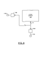
- FIG. 8 is a block diagram of two pad circuits sharing a signal.
- FIG. 9 is a flow diagram of a method of operation.
- each of the devices 100 A and 100 B generally includes multiple pins, balls, tabs, solder bumps or similar elements for externally interfacing to the devices 100 A and 100 B.
- the various pins, balls, tabs, solder bumps and the like may be referred to generally as a pin 102 , pins 102 and/or a specific pin X (where X is a pin number 1 ⁇ X ⁇ 64).
- Each device 100 A and 100 B may also include a package 104 .
- the device 100 A may be implemented as a 32-pin small outline integrated circuit (SOIC) package 104 A.
- SOIC small outline integrated circuit
- the device 100 B may be implemented as a 64-pin thin quad flat package (TQFP) 104 B.
- TQFP thin quad flat package
- the various package types 104 A and 104 B may be referred to generally as a package 104 and/or packages 104 .
- Other packages 104 and/or pin configurations may be implemented to meet the design criteria of a particular application using the invention.
- Both devices 100 A and 100 B may be implemented as processors. Functional differences between the device 100 A and the device 100 B may include, but are not limited to, a capability to interface to an external memory circuit (not shown) and/or a twisted pair transceiver capability. Other functions may be implemented within the device 100 A and/or the device 100 B to meet the design criteria of a particular application.
- the device 100 A may be implemented as two different devices or parts (e.g., P 1 and P 2 ).
- the device 100 B may be implemented as two different devices or parts (e.g., P 3 and P 4 ).
- the part P 1 may differ from the part P 2
- the part P 3 may differ from the part P 4 , based upon variations in signal assignments to one or more pins 102 .
- the part P 1 may assign a signal (e.g., CP 0 ) to a pin 19
- the part P 2 may assign another signal (e.g., T 1 ) to the same pin 19 .
- the part P 1 may assign a signal (e.g., CP 1 ) to a pin 20 and the part P 2 may assign another signal (e.g., T 2 ) to the pin 20 .
- the part P 3 may assign the signal CP 0 to a pin 28 and the part P 4 may assign the signal T 1 to the pin 28 .
- the part P 3 may assign the signal CP 1 to a pin 29 and the part P 4 may assign the signal T 2 to the pin 29 .
- the part P 1 generally comprises the package 104 A and a chip 106 .
- Other elements such as capacitors, resistors, inductors, and such may be included within the package 104 A along with the chip 106 .
- the chip 106 generally comprises a logic circuit 108 and a pad ring circuit 110 .
- the logic circuit 108 may provide the functionality of the devices 100 A–B and the parts P 1 –P 4 .
- the pad ring circuit 110 may provide for unidirectional inputs, unidirectional outputs, bidirectional input/outputs (IO), power, power returns or ground, clocks, reference signals and the like between the logic circuit 108 and the pins 102 .
- IO bidirectional input/outputs
- the pad ring circuit 110 generally comprises multiple pads 112 distributed along edges 114 A–D of the chip 106 . As shown in FIG. 3 , the edges 114 A–D may be referred to as a first edge 114 A, a second edge 114 B, a third edge 114 C and a fourth edge 114 D. Other number of edges and/or other edge references may be provided to meet the design criteria of a particular application.
- Each pad 112 along the first edge 114 A may be uniquely identified by reference letters AA through AR.
- the pads 112 along the second edge 114 B may be uniquely identified by reference letters BA through BR.
- the pads 112 along the third edge 114 C (e.g., a top edge in FIGS. 3 and 4 ) may be uniquely identified right to left by reference letters CA through CS.
- the pads 112 along the fourth edge 114 D (e.g., a left edge in FIGS. 3 and 4 ) may be uniquely identified by reference letters DA through DR.
- pads 112 along the edges 114 A–D may be implemented to meet the design criteria of a particular application. For example, a similar number of pads 112 may be positioned along each of the edges 114 A–D with the chip 106 having a generally square shape. In another example where the chip 106 has a generally rectangular shape, a greater number of pads 112 may be positioned along the longer edges 114 than along the shorter edges 114 .
- Wire bonds, tabs, solder bumps or similar elements may be used to connect the pads 112 to package traces 116 of the package 104 A. Each package trace 116 may be uniquely connected to a pin 102 .
- the wire bonds, tabs, solder bumps and such may be referred to generally as wire bonds 118 .
- references to connections between the pads 112 and the pins 102 may be inferred to include the wire bond 118 and the package trace 116 connections.
- pads 112 may be coupled to the same pins 102 for all four different parts P 1 –P 4 . Other pads 112 may be coupled to different pins 102 depending on the part P 1 –P 4 being implemented. Still other pads 112 may not be coupled to any pins 102 of any of the four parts P 1 –P 4 . Conversely, some of the pins 102 may not be coupled to any of the pads 112 . Various pads 112 may be coupled to the same pin 102 to help the logic circuit 108 and the pad ring circuit 110 identify the particular mode (e.g., M 1 or M 2 ), device 100 A– 100 B and/or part P 1 –P 4 being implemented. Example assignments of the pads 112 to the pins 102 for each of the modes M 1 –M 2 are shown in Tables I–IV as follows:
- the parts P 1 –P 4 may include a variety of signals, including power signals and ground signals.
- a list of the signals and associated functionality is generally provided in Table V as follows:
- the input to the configurable timer/counter 1 may be derived from pull-ups) one of the IO4–IO7.
- the input to the timer/counter 2 may be derived from the IO4.
- VDD Input Power input (5, 3.3 or 1.8 Vdc nominal)
- the chip 106 generally has a greater number of the pads 112 than a number of pins 102 for a largest package 104 being implemented.
- a first subset (e.g., S 1 ) of the pads 112 may be used to implement the part P 1 .
- a second subset (e.g., S 2 ) of the pads 112 may be used to implement the part P 2 .
- a third subset (e.g., S 3 ) of the pads 112 may be used to implement the part P 3 .
- a fourth subset (e.g., S 4 ) of the pads 112 may be used to implement the part P 4 .
- subsets may be defined to establish a different number of parts that may be created from the same chip 106 .
- two CHIP_SEL signals and three different packages 104 may define twelve subsets (four modes/package*three packages) for twelve different parts.
- only one subset S 1 –S 4 may be used at any time for fabricating the respective part P 1 –P 4 .
- the subsets S 1 and S 2 may bond a same number of the pads 112 to the pins 102 to implement the parts P 1 and P 2 .
- the first subset S 1 may include one or more pads 112 that are not within of the second subset S 2 .
- the second subset S 2 may also include one or more pads 112 that are not within of the first subset S 1 .
- the pins 19 and 20 may be bonded to the pads BN and BP for the part P 1 and to the pads BO and BQ for the part P 2 (dotted lines in FIG. 3 ).
- the pads BN and BP may be within the first subset S 1 but not the second subset S 2 .
- the pads BO and BP may be within the second subset S 2 but not the first subset S 1 .
- the subsets S 3 and S 4 may bond a same number of the pads 112 to the pins 102 to implement the parts P 3 and P 4 where the third subset S 3 is not identical to the fourth subset S 4 (dotted lines in FIG. 4 ).
- the subsets S 1 and S 3 may bond a different number of the pads 112 to the pins 102 to implement the parts P 1 and P 3 respectively.
- the subset S 3 may include address signals (e.g., A 0 –Al 5 ) not within the subset S 1 .
- the subset S 1 may include pads 112 not within the subset S 3 .
- the subset S 3 may include a power pad AQ (e.g., VDD) not within in the subset S 1 .
- the subsets S 2 and S 4 may bond a different number of the pads 112 to the pins 102 to implement the parts P 2 and P 4 respectively.
- the pads 112 may be used by multiple sets S 1 –S 4 to convey the same signal.
- the pad AD may be allocated to a signal (e.g., IO 1 ) for the parts P 1 , P 2 , P 3 and P 4 .
- Other pads 112 may be multiplexed to allocate different signals in the different modes M 1 –M 2 .
- the pad AC may be multiplexed to transfer a signal (e.g., IO 2 ) in the first mode M 1 and another signal (e.g., IO 0 ) in the second mode M 2 .
- a reset signal (e.g., /RESET) may be transferred on the pads AG and DO simultaneously.
- the signal /RESET may be coupled through the pad D 0 to the pin 1 and (ii) the pad AG may not be wire bonded to any pin 102 .
- the signal /RESET may be coupled through the pad AG to the pin 6 and (ii) the pad D 0 may not be wire bonded to any pin 102 .
- the particular pads 112 within each of the subsets S 1 –S 4 may be, but are not necessarily unique for a particular part P 1 –P 4 . Relationships among the subsets S 1 –S 4 may include intersections where one or more pads 112 are common to multiple subsets (e.g., non-empty intersections). Another relationship among the subsets S 1 –S 4 may include set differences where one or more pads 112 are included in a subset but not another subset. Still another relationship among the subsets S 1 –S 4 may include a minor subset being totally within a major subset where each pad 112 of the minor subset is also part of the major subset. Another relationship may be that two or more subsets are identical. Other subset relationships may be implemented to meet the design criteria of a particular application.
- wire bonding diagrams of the parts P 1 –P 4 respectively are shown. Connections between the pads 112 and the package traces 116 may be through wire bonds 118 or similar bonding methods. Each wire bond 118 may connect one or more pads 112 to a single package trace 116 of the package 104 .
- An example of a double bond among two pads 112 and one package trace 116 may be seen in FIG. 3 where the pads CI and CJ are both wire bonded to the package trace for the pin 23 coupleable to a ground or power return signal (e.g., VSS).
- VSS ground or power return signal
- pads CJ and CK are both wire bonded to the package trace for the pin 40 coupleable to a power signal (e.g., VDD).
- a power signal e.g., VDD.
- Some package traces 116 may not be wire bonded to any pad 112 .
- Some pads 112 may not be wire bonded to any package trace 116 .
- the logic circuit 108 generally comprises multiple processors 120 , 122 and 124 , multiple memory blocks 126 , 128 and 130 , a twisted pair transceiver 132 , a communications port 134 , a general purpose input/output (I/O) block 136 , a multiple timer/counter circuit 138 , an oscillator and clock and control circuit 140 , a memory map decoder (MMD) block 142 and a data/address bus 144 .
- An interface 146 may be provided by the parts P 3 and P 4 to couple to an external memory circuit (not shown).
- the logic circuit 108 may function as a node for a distributed intelligent control network. However, other appropriate logic functions may be executed by the chip 106 to meet the design criteria of a particular application.
- the MMD 142 may have an interface to receive a signal (e.g., MODE).
- the signal MODE may inform the logic circuit 108 of the package 104 A (e.g., 32-pin) or 104 B (e.g., 64-pin) being used. While the signal MODE is in the first mode M 1 (e.g., a logical LOW state), the logic circuit 108 may function as the parts P 1 or P 2 in the package 104 A. While the signal MODE is in the second mode M 2 (e.g., a logical HIGH state), the logic circuit 108 may function as the parts P 3 or P 4 in the package 104 B.
- a signal e.g., MODE
- Distinguishing between the parts P 1 and P 2 , and between the parts P 3 and P 4 may be accomplished by selectively wire bonding one or more predetermined signals (e.g., CP 0 and CP 1 or T 1 and T 2 ) to predetermined pins 102 .
- the signal MODE may have greater than two modes that may distinguish multiple parts and/or packages to meet the design criteria of a particular device family.
- the MMD 142 may establish a first memory mapping for the data/address bus 144 to map the addresses among the internal memory blocks 126 , 128 and 130 . While the signal MODE is in the second mode M 2 , the MMD 142 may establish another memory mapping for the data/address bus 144 to map the addresses among the internal memory blocks 126 , 128 and 130 and the external memory circuit (not shown) that may be coupled to the interface 146 .
- the circuit 148 generally comprises a source circuit 150 and a buffer circuit 152 .
- the source circuit 150 may generate and present a signal (e.g., CHIP_SEL) to the buffer circuit 152 .
- the buffer circuit 152 generally comprises one or more buffers 154 A–B.
- the buffers 154 A–B may buffer the signal CHIP_SEL to generate and present the signal MODE.
- the signal MODE may be distributed to the logic circuit 108 and/or throughout the pad ring circuit 110 .
- the source circuit 150 may be a pad 112 .
- the source circuit 150 may be the pad CJ.
- the pad CJ may be wire bonded to either a power signal VDD or a ground signal VSS to generate the signal CHIP_SEL. If the pad CJ is wire bonded to a ground signal VSS, the signal MODE may be in the first mode M 1 (e.g., the logical LOW state). If the pad CJ is wire bonded to a power signal VDD, the signal MODE may be in the second mode M 2 (e.g., the logical HIGH state).
- the pad CJ may be positioned between a pad 112 coupleable to a power signal VDD and another pad 112 coupleable to a ground signal VSS to make the double wire bonding to a nearby package trace 116 simple.
- the pad CJ may be adjacent to the ground pad CI that may be wire bonded to a ground signal VSS in the parts P 1 –P 4 .
- the pad CJ may also be positioned adjacent to the power pad CK that may be wire bonded to a power signal VDD in the parts P 3 and P 4 . (The pad CK may be unused in the parts P 1 and P 2 ).
- Multiple circuits 148 may be implemented to generate a multi-bit signal MODE that may represent greater than two possible modes or states.
- the pad CJ may be connected to the power signal VDD through tabs, solder bumps or the like in the parts P 3 and P 4 and to the signal VSS in the parts P 1 and P 2 .
- the source circuit 150 may be implemented as a programmable fuse, a register or a memory bit within the chip 106 .
- the source circuit 150 may be factory programmable and/or field programmable.
- the source circuit 150 may be a register, writeable through one or more processors 120 , 122 and 124 and/or pads 112 .
- the source circuit 150 may be a predetermined memory cell of the EEPROM memory circuit 128 or the ROM memory circuit 130 .
- the source circuit 150 may be a register that is part of a boundary-scan chain of registers.
- the register may be implemented in accordance with the Joint Test Action Group (JTAG) architecture defined by the Institute of Electrical and Electronics Engineering (IEEE) Standard 1149.1–1990, titled “IEEE Standard Test Access Port and Boundary-Scan Architecture”, published by the IEEE, New York, N.Y.
- JTAG Joint Test Action Group
- IEEE Institute of Electrical and Electronics Engineering
- CHIP_SEL Standard Test Access Port and Boundary-Scan Architecture
- the buffer circuit 152 may be implemented as a receive-only type of pad circuit. In another embodiment, the buffer circuit 152 may be implemented as a bidirectional type of pad circuit configured to receive at all times. Other designs for the buffer circuit 152 may be implemented to meet the design criteria of a particular application.
- the pad circuit 156 may be implemented as a bidirectional circuit that may drive a signal (e.g., DATA) onto a pad 112 and receive the signal DATA from the same pad 112 .
- the pad circuit 156 generally comprises a transceiver circuit 158 and an optional switching circuit 160 .
- the transceiver circuit 158 may be configured to amplify a signal (e.g., DOUT) to generate and present the signal DATA to the pad 112 .
- the signal DOUT may be implemented as a data output signal.
- Generation of the signal DATA may be performed in response to a controlling enable signal chosen from several enable signals (e.g., TXEN — 1–TXEN_N).
- the enable signals TXEN — 1–TXEN_N may be referred to generally as the enable signals TXEN.
- the enable signals TXEN may be generated by the logic circuit 108 . Some, all or none of the enable signals TXEN may be fixed to either the logical HIGH state or the logical LOW state instead of being controlled by the logic circuit 108 .
- Selection of a controlling enable signal TXEN_H may be determined by the signal MODE. While the controlling enable signal TXEN_H is asserted, the signal DATA may be generated with the same logical value as the signal DOUT. While the controlling enable signal TXEN_H is de-asserted, the transceiver circuit 158 may present a high impedance to the pad 112 .
- the transceiver circuit 158 may be configured to generate and present a signal (e.g., DIN) in response to receiving the signal DATA from the pad 112 .
- the signal DIN may be implemented as a data input signal. Generation of the signal DIN may be performed in response to a controlling enable signal chosen from several enable signals (e.g., RXEN — 1–RXEN_N).
- the enable signals RXEN — 1–RXEN_N may be referred to generally as the enable signals RXEN.
- the enable signals RXEN may be generated by the logic circuit 108 . Some, all or none of the enable signals RXEN may be fixed to the logical HIGH state or to the logical LOW state instead of being controlled by the logic circuit 108 .
- Selection of a controlling enable signal RXEN_H may be determined by the signal MODE. While the controlling enable signal RXEN_H is asserted, the signal DIN may be generated with the same logical state as the signal DATA. While the controlling enable signal RXEN_H is de-asserted, the transceiver circuit 158 may ignore the signal DATA.
- the switching circuit 160 may be configured to multiplex multiple signals (e.g., DOUT — 1–DOUT_N) to the signal DOUT and/or demultiplex the signal DIN to generate multiple signals (e.g., DIN — 1–DIN_N).
- Each of the signals DOUT — 1–DOUT_N may be implemented as a data output signal.
- Each of the signals DIN — 1–DIN_N may be implemented as a data input signal. Selections of the multiplexing and the demultiplexing functions are generally determined by the signal MODE.
- the switching circuit 158 may comprise a driver 162 , a receiver 164 , a multiplexer 166 and a multiplexer 168 .
- the driver 162 may be implemented as a tri-state driver that is generally enabled/disabled by an enable or control signal (e.g., TXCNT).
- the multiplexer 166 may multiplex the enable signals TXEN in response to the signal MODE to generate and present the signal TXCNT.
- the enable signals TXEN may be generated and presented by the logic circuit 108 . Some, all or none of the enable signals TXEN may be fixed to the logical HIGH state or the logical LOW state instead of being controlled by the logic circuit 108 .
- the receiver 164 may be implemented as a receiver that is generally enabled/disabled by an enable or control signal (e.g., RXCNT).
- the multiplexer 168 may multiplex the enable signals RXEN in response to the signal MODE to generate and present the signal RXCNT.
- the enable signals RXEN may be generated and presented by the logic circuit 108 . Some, all or none of the enable signals RXEN may be fixed to the logical HIGH state or the logical LOW state instead of being controlled by the logic circuit 108 .
- the switching circuit 160 generally comprises a multiplexer 170 and a demultiplexer 172 .
- the multiplexer 170 may be configured to multiplex the data output signals DOUT — 1–DOUT_N to generate and present the signal DOUT to the transceiver circuit 158 .
- the signal MODE may be used to control the multiplex selection of the multiplexer 170 .
- the demultiplexer 172 may be configured to demultiplex the signal DIN to present and generate the signals DIN — 1–DIN_N.
- the signal MODE may be used to control the demultiplex routing of the demultiplexer 172 .
- the pad circuit 156 may be configured as a transmit-only type of pad circuit. Transmit-only operations generally require the driver 162 , the multiplexer 166 and the multiplexer 170 . If there is only a single data output signal (e.g., DOUT — 1) in a particular design, the multiplexers 166 and 170 may be eliminated.
- DOUT — 1 data output signal
- the pad circuit 156 may be configured as a receive-only type of pad circuit. Receive-only operations generally require the receiver 164 , the multiplexer 168 and the demultiplexer 172 . If there is only a single data input signal (e.g., DIN — 1) in a particular design, the multiplexer 168 and the de-multiplexer 172 may be eliminated.
- a single data input signal e.g., DIN — 1
- a trace or signal line 174 may transfer a signal (e.g., X) between the logic circuit 108 and a first pad circuit 156 A.
- the first pad circuit 156 A may be connected to a first pad 112 A to allow the signal X to be transmitted or received externally from/to the device 100 .
- the signal line 174 may also carry the signal X to a second pad circuit 156 B located at a distance from the first pad circuit 156 A.
- the second pad circuit 156 B may be connected to a second pad 112 B to allow the signal X to be transmitted or received externally from/to the device 100 .
- the first and the second pad circuit 156 A–B may be configured such that the signal X may be passed between the logic circuit 108 and only one of the first or the second pads 112 A–B at a time.
- the second pad signal 156 B may block the signal X from the second pad 112 B.
- the signal X may be an I/O signal (e.g., IO 3 )
- the first pad 112 A may be the pad AA
- the second pad 112 B may be the pad AF.
- the first pad circuit 156 A may transfer the signal IO 3 between the logic circuit 108 and the pad AA while the second pad circuit 156 B blocks the signal IO 3 from the pad AF. While the signal MODE is in the second mode M 2 , the first pad circuit 156 A may block the signal IO 3 from the pad AA while the second pad circuit 156 B transfers the signal 103 between the logic circuit 108 and the pad AF.
- the first and the second pad circuits 156 A–B may be configured to pass the signal X between the logic circuit 108 and both the first and the second pads 112 A–B simultaneously.
- the signal X may be a service signal (e.g., /SERVICE)
- the first pad 112 A may be the pad AI
- the second pad 112 B may be the pad BC.
- the signal /SERVICE may alternate between simultaneous transmission and simultaneous reception at both pads AI and BC. Therefore, the parts P 1 and P 2 may wire bond the pad AI to the pin 8 to transfer the signal /SERVICE while the pad BC is left unconnected.
- the parts P 3 and P 4 may wire bond the pad BC to the pin 17 to transfer the signal /SERVICE while the pad AI is left unconnected.
- the method generally begins with a generation of the signal MODE (e.g., block 176 ).
- the logic circuit 108 may respond to the signal MODE by configuring to the appropriate device 100 A–B and/or part group P 1 /P 2 or P 3 /P 4 (e.g., block 178 ).
- the pads 112 and the pad circuit 156 may also respond to the signal MODE by configuring for to the indicated part group P 1 /P 2 or P 3 /P 4 (e.g., block 180 ).
- the adjoining pad circuit 156 A may buffer the data input signal (e.g., block 182 ).
- the same data input signal, or a different data input signal may simultaneously and independently be received by a second pad 112 B and buffered by a second pad circuit 156 B (e.g., block 184 ).
- the first pad circuit 156 A may demultiplex the data input signal onto an appropriate signal line coupled to the logic circuit 108 (e.g., block 186 ).
- the second pad circuit 156 B may demultiplex the data input signal onto a signal line determined by the signal MODE (e.g., block 188 ).
- the data input signal received by both pads 112 A and 112 B may be the same signal. Therefore, the first and the second pad circuits 156 A and 156 B may demultiplex the data input signal onto a shared or common signal line 174 coupled to the logic circuit 108 (e.g., block 190 ).
- the first pad circuit 156 A may multiplex one or more a data output signals presented by the logic circuit 108 as determined by the signal MODE (e.g., block 192 ).
- the second pad circuit 156 B may simultaneously and independently multiplex one or more data output signals presented by the logic circuit 108 as determined by the signal MODE (e.g., block 194 ).
- the first and the second pad circuits 156 A and 156 B may multiplex different signals received on different signal lines and/or the same signal received on a common signal line (e.g., block 190 ).
- the first pad circuit 156 A may then drive the selected data output signal onto the first pad 112 A (e.g., block 196 ).
- the second pad circuit 156 B may drive the selected data output signal onto the second pad 112 B (e.g., block 198 ).
- the sequence of receiving and transmitting signals on the various pads may be altered to meet the design criteria of a particular application.
- some pads 112 may be receiving data signals while other pads 112 are simultaneously transmitting other data signals.
- each pad 112 and pad circuit 156 pair may operate independently of all other pads 112 and pad circuit 156 pairs. Exceptions to the independent operation may exist for signals such as the signal /RESET an the signal /SERVICE that may be designed to operate with two pad circuits 156 and two pads 112 in parallel.
- the single chip design may be fabricated from a predetermined set of masks. Once fabricated, the chip 106 may be tested and qualified using a common set of procedures. An overall effect may be to reduce the cost of the parts P 1 –P 4 by using the single chip design instead of four unique designs.
- the various signals of the present invention are generally “on” (e.g., a digital HIGH, or 1) or “off” (e.g., a digital LOW, or 0).
- the particular polarities of the on (e.g., asserted) and off (e.g., de-asserted) states of the signals may be adjusted (e.g., reversed) accordingly to meet the design criteria of a particular implementation.
- inverters may be added to change a particular polarity of the signals.
- the term “simultaneously” is meant to describe events that share some common time period but the term is not meant to be limited to events that begin at the same point in time, end at the same point in time, or have the same duration.
Abstract
Description
| TABLE |
| First Edge |
| 114A |
| Pad | Mode M1 | Part P1 | Part P2 | Mode M2 | Part P3 | Part P4 |
| No. | Signal | Pin No. | Pin No. | Signal | Pin No. | Pin No. |
| | IO3 | 4 | 4 | |
64 | 64 | |
| AB | Not used | |
1 | 1 | |||
| | IO2 | 5 | 5 | |
2 | 2 | |
| | IO1 | 6 | 6 | |
3 | 3 | |
| | IO0 | 7 | 7 | |
4 | 4 | |
| AF | Not used | |
5 | 5 | |||
| AG | Not used | / |
6 | 6 | |||
| AH | Not used | |
7 | 7 | |||
| AI | / |
8 | 8 | Not used | |||
| | VSS | 9 | 9 | |
8 | 8 | |
| | VPP | 10 | 10 | |
9 | 9 | |
| AL | Not used | |
10 | 10 | |||
| AM | Not used | |
11 | 11 | |||
| AN | Not used | |
12 | 12 | |||
| | VDD | 11 | 11 | Not used | |||
| AP | Not used | |
13 | 13 | |||
| | VDD | 12 | 12 | Not used | |||
| AR | Not used | |
14 | 14 | |||
| TABLE |
| Second Edge |
| 114B |
| Pad | Mode M1 | Part P1 | Part P2 | Mode M2 | Part P3 | Part P4 |
| No. | Signal | Pin No. | Pin No. | Signal | Pin No. | Pin No. |
| BA | Not used | |
15 | 15 | |||
| BB | Not used | |
16 | 16 | |||
| BC | Not used | / |
17 | 17 | |||
| BD | Not used | |
18 | 18 | |||
| | VSS | 13 | 13 | |
19 | 19 | |
| BF | Not used | |
20 | 20 | |||
| BG | Not used | |
21 | 21 | |||
| BH | Not used | |
22 | 22 | |||
| | CLK2 | 14 | 14 | |
23 | 23 | |
| | CLK1 | 15 | 15 | CLK1 | 24 | 24 | |
| | VSS | 16 | 16 | |
25 | 25 | |
| | CP2 | 17 | 17 | Not used | |||
| | VDD | 18 | 18 | |
26 | 26 | |
| | CP0 | 19 | |
28 | |||
| | T1 | 19 | |
28 | |||
| | CP1 | 20 | |
29 | |||
| | T2 | 20 | |
29 | |||
| BR | Not used | |
30 | 30 | |||
| TABLE |
| Third Edge |
| 114C |
| Pad | Mode M1 | Part P1 | Part P2 | Mode M2 | Part P3 | Part P4 |
| No. | Signal | Pin No. | Pin No. | Signal | Pin No. | Pin No. |
| | CP3 | 21 | 21 | |
31 | 31 | |
| | CP4 | 22 | 22 | CP4 | 32 | 32 | |
| CC | Not used | |
33 | 33 | |||
| CD | Not used | |
34 | 34 | |||
| CE | Not used | |
35 | 35 | |||
| CF | Not used | |
36 | 36 | |||
| CG | Not used | |
37 | 37 | |||
| CH | Not used | |
38 | 38 | |||
| | VSS | 23 | 23 | |
39 | 39 | |
| | CHIP_SEL | 23 | 23 | |
40 | 40 | |
| CK | Not used | |
40 | 40 | |||
| CL | Not used | |
41 | 41 | |||
| CM | Not used | |
42 | 42 | |||
| | IO10 | 24 | 24 | |
43 | 43 | |
| | VDD | 25 | 25 | |
44 | 44 | |
| | IO9 | 26 | 26 | R/ |
45 | 45 | |
| | IO8 | 27 | 27 | / |
46 | 46 | |
| | IO7 | 28 | 28 | |
47 | 47 | |
| | IO6 | 29 | 29 | A14 | 50 | 50 | |
| TABLE |
| Fourth Edge |
| 114D |
| Pad | Mode M1 | Part P1 | Part P2 | Mode M2 | Part P3 | Part P4 |
| No. | Signal | Pin No. | Pin No. | Signal | Pin No. | Pin No. |
| | IO5 | 30 | 30 | |
51 | 51 | |
| DB | Not used | |
52 | 52 | |||
| | VSS | 31 | 31 | Not used | |||
| | VDD | 32 | 32 | Not used | |||
| DE | Not used | |
53 | 53 | |||
| DF | Not used | |
54 | 54 | |||
| DG | Not used | |
55 | 55 | |||
| DH | Not used | |
56 | 56 | |||
| DI | Not used | |
57 | 57 | |||
| DJ | Not used | |
58 | 58 | |||
| DK | Not used | |
59 | 59 | |||
| DL | Not used | |
60 | 60 | |||
| DM | Not used | |
61 | 61 | |||
| DN | Not used | |
62 | 62 | |||
| DO | / |
1 | 1 | Not used | |||
| | VDD | 2 | 2 | Not used | |||
| | IO4 | 3 | 3 | |
63 | 63 | |
| DR | Not used | Not used | |||||
| TABLE V |
| Signals |
| Signal | ||
| Name | Direction | Signal Function |
| CLK1 | Input | Oscillator connection or external |
| clock input | ||
| CLK2 | Output | Oscillator connection. Leave open |
| when external clock in input to CLK1. | ||
| /RESET | I/O (Built-in | Active LOW reset |
| pull-up) | ||
| /SERVICE | I/O (Built-in | Alternates between input and output |
| configurable | at a 76 Hz rate | |
| pull-up) | ||
| IO0–IO3 | I/O | General I/O ports with a large |
| current-sink capacity. The output of | ||
| the time/ |
||
| IO0. The output of timer/ |
||
| may be routed to IO1. | ||
| IO4–IO7 | I/O (Built-in | General I/O ports. The input to the |
| configurable | timer/ |
|
| pull-ups) | one of the IO4–IO7. The input to the | |
| timer/ |
||
| the IO4. | ||
| IO8–IO10 | I/O | General I/O port. May be used for |
| serial communications under firmware | ||
| control. | ||
| D0–D7 | I/O | Bidirectional memory data bus. |
| R/W | Output | Read/write control output for |
| external memory. | ||
| /E | Output | Enable clock control output for the |
| external memory. | ||
| A0–A15 | Output | Memory address output port. |
| VDD | Input | Power input (5, 3.3 or 1.8 Vdc |
| nominal) | ||
| VSS | Input | Power input (0 Vdc ground) |
| VPP | INPUT | In-circuit rest mode control. If VPP |
| is high when /RESET is asserted, the | ||
| I/O, addresses and data buses become | ||
| high-impedance. | ||
| CP0–CP4 | Communications | Bidirectional port supporting |
| Network | communications in three modes. | |
| Interface | ||
| T1–T2 | Bidirectional | Differential analog signals used to |
| interface with a free topology | ||
| network through a transformer. | ||
| NC | N/A | No connect. Must not be connected on |
| the user's board. | ||
Claims (19)
Priority Applications (1)
| Application Number | Priority Date | Filing Date | Title |
|---|---|---|---|
| US10/134,764 US7170179B1 (en) | 2002-04-29 | 2002-04-29 | Chip select method through double bonding |
Applications Claiming Priority (1)
| Application Number | Priority Date | Filing Date | Title |
|---|---|---|---|
| US10/134,764 US7170179B1 (en) | 2002-04-29 | 2002-04-29 | Chip select method through double bonding |
Publications (1)
| Publication Number | Publication Date |
|---|---|
| US7170179B1 true US7170179B1 (en) | 2007-01-30 |
Family
ID=37681874
Family Applications (1)
| Application Number | Title | Priority Date | Filing Date |
|---|---|---|---|
| US10/134,764 Expired - Lifetime US7170179B1 (en) | 2002-04-29 | 2002-04-29 | Chip select method through double bonding |
Country Status (1)
| Country | Link |
|---|---|
| US (1) | US7170179B1 (en) |
Cited By (6)
| Publication number | Priority date | Publication date | Assignee | Title |
|---|---|---|---|---|
| CN101510535B (en) * | 2009-04-03 | 2010-11-03 | 智原科技股份有限公司 | Output/input unit for implementing chip and method for manufacturing chip |
| US20100277150A1 (en) * | 2008-01-11 | 2010-11-04 | Ricoh Company, Ltd. | Semiconductor device and manufacturing method thereof |
| US8324929B1 (en) * | 2008-02-04 | 2012-12-04 | Netlogic Microsystems, Inc. | Integrated circuit with reconfigurable inputs/outputs |
| US20190007048A1 (en) * | 2017-06-28 | 2019-01-03 | Texas Instruments Incorporated | Integrated circuit and process for family of digital logic functions |
| CN110120877A (en) * | 2018-02-05 | 2019-08-13 | 大唐移动通信设备有限公司 | A kind of configuration method of the parameter of the configuration circuit and exchange chip of exchange chip |
| CN112927747A (en) * | 2021-04-22 | 2021-06-08 | 中科一芯科技(深圳)有限公司 | Method for solving chip failure caused by routing of embedded memory chip |
Citations (10)
| Publication number | Priority date | Publication date | Assignee | Title |
|---|---|---|---|---|
| US5181201A (en) | 1990-02-07 | 1993-01-19 | General Dynamics Land Systems Inc. | Interface chip device |
| US5796266A (en) * | 1996-03-18 | 1998-08-18 | Micron Technology, Inc. | Circuit and a method for configuring pad connections in an integrated device |
| US5872737A (en) * | 1996-11-01 | 1999-02-16 | Mitsubishi Denki Kabushiki Kaisha | Semiconductor integrated circuit device in which influence of power supply noise on internal circuitry during operation of input/output buffer is prevented |
| US5991232A (en) * | 1998-02-03 | 1999-11-23 | Mitsubishi Denki Kabushiki Kaisha | Clock synchronous memory embedded semiconductor integrated circuit device |
| US6038188A (en) * | 1993-06-17 | 2000-03-14 | Matsushita Electric Industrial Co., Ltd. | Data transmission circuit, data line driving circuit, amplifying circuit, semiconductor intergrated circuit, and semiconductor memory |
| US6180426B1 (en) * | 1999-03-01 | 2001-01-30 | Mou-Shiung Lin | High performance sub-system design and assembly |
| US6242737B1 (en) * | 1997-08-21 | 2001-06-05 | Japan Science And Technology Corporation | Microscopic system equipt with an electron microscope and a scanning probe microscope |
| US6353333B1 (en) * | 2000-06-16 | 2002-03-05 | Xilinx, Inc. | Simplified 5V tolerance circuit for 3.3V I/O design |
| US6586266B1 (en) * | 1999-03-01 | 2003-07-01 | Megic Corporation | High performance sub-system design and assembly |
| US6597602B2 (en) * | 2000-09-22 | 2003-07-22 | Kabushiki Kaisha Toshiba | Semiconductor memory device |
-
2002
- 2002-04-29 US US10/134,764 patent/US7170179B1/en not_active Expired - Lifetime
Patent Citations (10)
| Publication number | Priority date | Publication date | Assignee | Title |
|---|---|---|---|---|
| US5181201A (en) | 1990-02-07 | 1993-01-19 | General Dynamics Land Systems Inc. | Interface chip device |
| US6038188A (en) * | 1993-06-17 | 2000-03-14 | Matsushita Electric Industrial Co., Ltd. | Data transmission circuit, data line driving circuit, amplifying circuit, semiconductor intergrated circuit, and semiconductor memory |
| US5796266A (en) * | 1996-03-18 | 1998-08-18 | Micron Technology, Inc. | Circuit and a method for configuring pad connections in an integrated device |
| US5872737A (en) * | 1996-11-01 | 1999-02-16 | Mitsubishi Denki Kabushiki Kaisha | Semiconductor integrated circuit device in which influence of power supply noise on internal circuitry during operation of input/output buffer is prevented |
| US6242737B1 (en) * | 1997-08-21 | 2001-06-05 | Japan Science And Technology Corporation | Microscopic system equipt with an electron microscope and a scanning probe microscope |
| US5991232A (en) * | 1998-02-03 | 1999-11-23 | Mitsubishi Denki Kabushiki Kaisha | Clock synchronous memory embedded semiconductor integrated circuit device |
| US6180426B1 (en) * | 1999-03-01 | 2001-01-30 | Mou-Shiung Lin | High performance sub-system design and assembly |
| US6586266B1 (en) * | 1999-03-01 | 2003-07-01 | Megic Corporation | High performance sub-system design and assembly |
| US6353333B1 (en) * | 2000-06-16 | 2002-03-05 | Xilinx, Inc. | Simplified 5V tolerance circuit for 3.3V I/O design |
| US6597602B2 (en) * | 2000-09-22 | 2003-07-22 | Kabushiki Kaisha Toshiba | Semiconductor memory device |
Cited By (13)
| Publication number | Priority date | Publication date | Assignee | Title |
|---|---|---|---|---|
| US20100277150A1 (en) * | 2008-01-11 | 2010-11-04 | Ricoh Company, Ltd. | Semiconductor device and manufacturing method thereof |
| KR101224251B1 (en) * | 2008-01-11 | 2013-01-21 | 가부시키가이샤 리코 | Semiconductor device and testing method thereof |
| US8575904B2 (en) * | 2008-01-11 | 2013-11-05 | Ricoh Company, Ltd. | Semiconductor device and manufacturing method thereof |
| US8324929B1 (en) * | 2008-02-04 | 2012-12-04 | Netlogic Microsystems, Inc. | Integrated circuit with reconfigurable inputs/outputs |
| CN101510535B (en) * | 2009-04-03 | 2010-11-03 | 智原科技股份有限公司 | Output/input unit for implementing chip and method for manufacturing chip |
| US11251795B2 (en) | 2017-06-28 | 2022-02-15 | Texas Instruments Incorporated | IC with first and second functional circuits coupling only first circuits to output bond pads |
| US20190007048A1 (en) * | 2017-06-28 | 2019-01-03 | Texas Instruments Incorporated | Integrated circuit and process for family of digital logic functions |
| US10693468B2 (en) * | 2017-06-28 | 2020-06-23 | Texas Instruments Incorporated | Integrated circuit and process for family of digital logic functions |
| US20220140830A1 (en) * | 2017-06-28 | 2022-05-05 | Texas Instruments Incorporated | Ic with first and second functional circuits coupling only first circuits to output bond pads |
| CN110120877A (en) * | 2018-02-05 | 2019-08-13 | 大唐移动通信设备有限公司 | A kind of configuration method of the parameter of the configuration circuit and exchange chip of exchange chip |
| CN110120877B (en) * | 2018-02-05 | 2020-11-20 | 大唐移动通信设备有限公司 | Configuration circuit of exchange chip and configuration method of parameters of exchange chip |
| CN112927747B (en) * | 2021-04-22 | 2021-09-21 | 中科一芯科技(深圳)有限公司 | Method for solving chip failure caused by routing of embedded memory chip |
| CN112927747A (en) * | 2021-04-22 | 2021-06-08 | 中科一芯科技(深圳)有限公司 | Method for solving chip failure caused by routing of embedded memory chip |
Similar Documents
| Publication | Publication Date | Title |
|---|---|---|
| US6266797B1 (en) | Data transfer network on a computer chip using a re-configurable path multiple ring topology | |
| CN105679748B (en) | Method and apparatus for testing accessory in multi-chip encapsulation body | |
| CN100421174C (en) | Stacked layered type semiconductor memory device | |
| US8269524B2 (en) | General purpose input/output pin mapping | |
| US20080079148A1 (en) | Package for mixed signal mcu with minimal pin count | |
| US6275975B1 (en) | Scalable mesh architecture with reconfigurable paths for an on-chip data transfer network incorporating a network configuration manager | |
| KR20060079848A (en) | Multiplexing of digital signals at multiple supply voltages in integrated circuit | |
| US7818640B1 (en) | Test system having a master/slave JTAG controller | |
| CN111741601B (en) | Universal configurable active substrate circuit structure | |
| US7170179B1 (en) | Chip select method through double bonding | |
| US20130214389A1 (en) | Integrated circuit | |
| CN1937408A (en) | Programmable logic device architecture for accommodating specialized circuitry | |
| US6271587B1 (en) | Connection arrangement for enbaling the use of identical chips in 3-dimensional stacks of chips requiring address specific to each chip | |
| US7239260B2 (en) | Analog-to-digital interfacing device and method of analog-to-digital interfacing | |
| US7253660B1 (en) | Multiplexing device including a hardwired multiplexer in a programmable logic device | |
| JP2002057270A (en) | Stacked chip semiconductor device | |
| US5689462A (en) | Parallel output buffers in memory circuits | |
| US20050055618A1 (en) | Test arrangement and method for selecting a test mode output channel | |
| US20220109446A1 (en) | Systems And Methods For Configurable Interface Circuits | |
| US20040188853A1 (en) | Semiconductor device | |
| US6950324B2 (en) | Memory device composed of a plurality of memory chips in a single package | |
| US6452417B1 (en) | I/O cell architecture for CPLDs | |
| JP2011204821A (en) | Semiconductor device | |
| US7429794B2 (en) | Multi-chip packaged integrated circuit device for transmitting signals from one chip to another chip | |
| US20030122576A1 (en) | Pad system for an integrated circuit or device |
Legal Events
| Date | Code | Title | Description |
|---|---|---|---|
| AS | Assignment |
Owner name: CYPRESS SEMICONDUCTOR CORPORATION, CALIFORNIA Free format text: ASSIGNMENT OF ASSIGNORS INTEREST;ASSIGNOR:SHAH, SHAILESH;REEL/FRAME:012856/0352 Effective date: 20020428 |
|
| STCF | Information on status: patent grant |
Free format text: PATENTED CASE |
|
| FPAY | Fee payment |
Year of fee payment: 4 |
|
| FEPP | Fee payment procedure |
Free format text: PAYOR NUMBER ASSIGNED (ORIGINAL EVENT CODE: ASPN); ENTITY STATUS OF PATENT OWNER: LARGE ENTITY |
|
| FPAY | Fee payment |
Year of fee payment: 8 |
|
| AS | Assignment |
Owner name: MORGAN STANLEY SENIOR FUNDING, INC., NEW YORK Free format text: SECURITY INTEREST;ASSIGNORS:CYPRESS SEMICONDUCTOR CORPORATION;SPANSION LLC;REEL/FRAME:035240/0429 Effective date: 20150312 |
|
| MAFP | Maintenance fee payment |
Free format text: PAYMENT OF MAINTENANCE FEE, 12TH YEAR, LARGE ENTITY (ORIGINAL EVENT CODE: M1553) Year of fee payment: 12 |
|
| AS | Assignment |
Owner name: CYPRESS SEMICONDUCTOR CORPORATION, CALIFORNIA Free format text: PARTIAL RELEASE OF SECURITY INTEREST IN PATENTS;ASSIGNOR:MUFG UNION BANK, N.A., AS COLLATERAL AGENT;REEL/FRAME:050500/0112 Effective date: 20190925 Owner name: SPANSION LLC, CALIFORNIA Free format text: PARTIAL RELEASE OF SECURITY INTEREST IN PATENTS;ASSIGNOR:MUFG UNION BANK, N.A., AS COLLATERAL AGENT;REEL/FRAME:050500/0112 Effective date: 20190925 |
|
| AS | Assignment |
Owner name: MONTEREY RESEARCH, LLC, CALIFORNIA Free format text: ASSIGNMENT OF ASSIGNORS INTEREST;ASSIGNOR:CYPRESS SEMICONDUCTOR CORPORATION;REEL/FRAME:050829/0230 Effective date: 20190925 |
|
| AS | Assignment |
Owner name: MUFG UNION BANK, N.A., CALIFORNIA Free format text: ASSIGNMENT AND ASSUMPTION OF SECURITY INTEREST IN INTELLECTUAL PROPERTY;ASSIGNOR:MORGAN STANLEY SENIOR FUNDING, INC.;REEL/FRAME:050896/0366 Effective date: 20190731 |
|
| AS | Assignment |
Owner name: MORGAN STANLEY SENIOR FUNDING, INC., NEW YORK Free format text: CORRECTIVE ASSIGNMENT TO CORRECT THE 8647899 PREVIOUSLY RECORDED ON REEL 035240 FRAME 0429. ASSIGNOR(S) HEREBY CONFIRMS THE SECURITY INTERST;ASSIGNORS:CYPRESS SEMICONDUCTOR CORPORATION;SPANSION LLC;REEL/FRAME:058002/0470 Effective date: 20150312 |