US7171127B2 - Optical transmission controller - Google Patents
Optical transmission controller Download PDFInfo
- Publication number
- US7171127B2 US7171127B2 US10/717,283 US71728303A US7171127B2 US 7171127 B2 US7171127 B2 US 7171127B2 US 71728303 A US71728303 A US 71728303A US 7171127 B2 US7171127 B2 US 7171127B2
- Authority
- US
- United States
- Prior art keywords
- waveform
- section
- optical signal
- semiconductor laser
- bias current
- Prior art date
- Legal status (The legal status is an assumption and is not a legal conclusion. Google has not performed a legal analysis and makes no representation as to the accuracy of the status listed.)
- Expired - Fee Related, expires
Links
Images


Classifications
-
- H—ELECTRICITY
- H04—ELECTRIC COMMUNICATION TECHNIQUE
- H04B—TRANSMISSION
- H04B10/00—Transmission systems employing electromagnetic waves other than radio-waves, e.g. infrared, visible or ultraviolet light, or employing corpuscular radiation, e.g. quantum communication
- H04B10/50—Transmitters
- H04B10/501—Structural aspects
- H04B10/503—Laser transmitters
- H04B10/504—Laser transmitters using direct modulation
Definitions
- the present invention relates to an optical transmission controller. More particularly, the present invention relates to an optical transmission controller which has application in the field of optical communications and which employs a semiconductor laser as a light source for optical signal transmission.
- optical communications are finding increased use as a means for transmission of information. They are currently used mainly in trunk line systems, but are predicted to have application in apparatus-to-apparatus communications and in networked systems in correspondence with the computerization in offices and households as they are expected to be in widespread use.
- optical fibers as a communication medium and transmit/receive apparatuses for transmitting/receiving light.
- plastic fibers be used since they are inexpensive as a medium and excellent in their connectivity to apparatuses for a low-cost construction of optical communication systems.
- the use of plastic fibers is advantageous in that a red semiconductor laser (operated with ⁇ in the vicinity of 650 nm) is available as an inexpensive light source in the use of plastic fibers since recent years have seen a remarkable proliferation of the red semiconductor laser for use as a DVD device laser.
- an oscillation threshold current is constantly provided as a bias current to a semiconductor laser and a modulation current is superposed on the oscillation threshold current for generating modulation light.
- a modulation current is superposed on the oscillation threshold current for generating modulation light.
- One measure to meet the demand is considered to be to reduce the bias current in driving the semiconductor laser.
- the reduction of the bias current is achieved as follows. When the semiconductor laser is driven starting with a bias current not higher than the oscillation threshold value, an oscillation delay occurs in the laser. It is assumed, however, that this raises no problem as long as systems are used in a range permitted by the specifications of the systems or as long as the semiconductor laser is driven so as to compensate the delay in pulse width.
- an optical signal output hereafter, also referred to simply as “an optical output”.
- a modulation signal frequency is high, a modulation is effected before the relaxation oscillation does not subside yet.
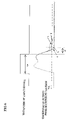
- a fall state of a waveform of the optical output is subject to the relaxation oscillation.
- the injection electron density n continues to increase beyond the threshold electron density nth, and then turns to decrease with increase in the photon density nph (with increase in light emission).
- the photon density nph turns to decrease.
- the photon density nph becomes sufficiently small when the injection electron density n, which once has decreased to a value not higher than the threshold electron density nth, again turns to increase to reach the threshold electron density nth.
- This transient phenomenon is called relaxation oscillation.
- the time to switch off the input current (input signal) will be examined.
- the fall portion of the waveform of the optical output is not subject to the relaxation oscillation.
- the input current is switched off during the relaxation oscillation, however, the fall portion of the optical output waveform is subject to the relaxation oscillation.
- the input current is switched off at times t 1 , t 2 , t 3 and t 4 .
- the times t 1 , t 2 , t 3 and t 4 are four typical times in one variation period of the injection electron density n (one period of the relaxation oscillation).
- the time t 1 is where the injection electron density n turns from increase to decrease
- the time t 2 is where the injection electron density n is on the decrease at the threshold electron density nth
- the time t 3 is where the injection electron density n turns from decrease to increase
- the time t 4 is where the injection electron density n is on the increase at the threshold electron density nth.
- waveforms ⁇ circle around ( 1 ) ⁇ to ⁇ circle around ( 4 ) ⁇ of FIG. 5 are ones obtained by switching off the input current (input signal) at the times t 1 , t 2 , t 3 and t 4 , respectively.
- the fall state of the waveform of the injection electron density n (optical output waveform) varies depending on when the input current is switched off.
- the waveforms ⁇ circle around ( 3 ) ⁇ and ⁇ circle around ( 4 ) ⁇ compared to the waveforms ⁇ circle around ( 1 ) ⁇ and ⁇ circle around ( 2 ) ⁇ increase the injection electron density n even after the input current is switched off so that light is emitted with the injection electron density n above the threshold electron density nth.
- the waveforms ⁇ circle around ( 3 ) ⁇ and ⁇ circle around ( 4 ) ⁇ have further oscillation crests after the input current is switched off. This serves to deteriorate the fall state of the waveform of the optical output and to prolong a fall time thereof. With such optical waveforms, an Eye Opening cannot be ensured in waveforms obtained during communication, and thereby the communication quality is significantly deteriorated. Further, lowering the communication speed becomes necessary for ensuring the communication quality.
- the fall portion of the optical output waveform is subject to the relaxation oscillation depending on when the input signal is switched off, and thereby the communication quality is deteriorated and the high-speed communication is impaired.
- the present invention has been made in view of the above circumstances and the purpose thereof is to improve a waveform of a fall portion of an optical output when a high-speed drive of a semiconductor laser is performed starting with a value not higher than an oscillation threshold value for its low power drive by appropriately selecting the switching-off timing of an input current with respect to a relaxation oscillation of the optical output.
- the present invention provides an optical transmission controller comprising: a semiconductor laser; a semiconductor laser drive section for allowing the semiconductor laser to output an optical signal; a monitor photoreceptor for monitoring the optical signal output from the semiconductor laser; a waveform detection means for detecting a fall state of a waveform of the optical signal output monitored by the monitor photoreceptor; and a phase relation adjustment means for adjusting a phase relation between a fall timing of an input current fed to the semiconductor laser and a variation timing of a relaxation oscillation of the waveform of the optical signal output in accordance with a detection result of the waveform detection means to reduce a relaxation oscillation of a fall portion of the waveform of the optical signal output.
- the phase relation between the fall timing of the input current fed to the semiconductor laser and the variation timing of the relaxation oscillation of the waveform of the optical signal output is adjusted to reduce the relaxation oscillation of the fall portion of the waveform of the optical signal output. This allows a flat waveform of the optical signal output to be obtained which is free from a transient oscillation otherwise occurring at the fall portion, thereby preventing deterioration in quality of communication that uses the optical signal.
- FIG. 1 is an explanatory view illustrating a construction of Embodiment 1 of the present invention
- FIG. 2 is an explanatory view illustrating a construction of Embodiment 2 of the present invention.
- FIG. 3 is an explanatory view illustrating a construction of Embodiment 3 of the present invention.
- FIG. 4 is an explanatory view illustrating a construction of Embodiment 4 of the present invention.
- FIG. 5 is an explanatory view for a relaxation oscillation of an optical output
- FIG. 6 is an explanatory view illustrating the phase relation between the switching-off timing of an input signal and the relaxation oscillation
- FIG. 7 is a flowchart illustrating a procedure for setting a bias current in Embodiment 1;
- FIG. 8 is a flowchart illustrating a procedure for setting a modulation current in Embodiment 2;
- FIG. 9 is a flowchart illustrating a procedure for setting the bias current and the modulation current in Embodiment 3.
- FIG. 10 is an explanatory view illustrating the details of an input signal control section of FIG. 4 ;
- FIG. 11 is a time chart for explaining a delay in the switching-off timing of an input signal in Embodiment 4.
- FIG. 12 is a flowchart illustrating a procedure for varying the switching-off timing of an input signal by means of the input signal control section.
- the present invention improves a fall portion of an optical output when a high-speed drive of a semiconductor laser is performed starting with a value not higher than an oscillation threshold value for its low power drive by appropriately selecting the switching-off timing of an input current with respect to a relaxation oscillation of the optical output.
- the phase relation adjustment means includes the following three means:
- a bias current setting means is for adjusting the bias current of the semiconductor laser within a range between values smaller than an oscillation threshold value to vary a delay time in the optical signal output against the input current to vary a phase of the relaxation oscillation of the waveform of the optical signal output with respect to the fall timing of the input current.
- the bias current setting means is for varying a rise timing of the input current (delay time in the optical signal output) with respect to a switching-on timing of the input signal (input current) to vary the phase of the relaxation oscillation of the waveform of the optical signal output with respect to a switching-off timing of the input signal.
- An appropriate period which the variation in the delay time in the optical signal output against the input current is caused by adjusting the bias current is not longer than one period of the relaxation oscillation of the optical signal output.
- a bias current setting means is for adjusting the input current to vary a frequency of the relaxation oscillation of the waveform of the optical signal output and thereby to vary the phase of the relaxation oscillation of the waveform of the optical signal output with respect to the fall timing of the input current.
- the bias current setting means is for varying the frequency of the relaxation oscillation of the output waveform of the optical signal to vary the phase of the relaxation oscillation with respect to the switching-off timing of the input current.
- the frequency of the relaxation oscillation becomes higher with a larger value I of the modulation current (input current).
- An input signal control means is for adjusting the switching-off timing of the input signal to vary the phase of the relaxation oscillation of the waveform of the optical signal output with respect to the fall timing of the input current.
- the input signal control means is for varying the switching-off timing of the input signal with respect to the relaxation oscillation of the waveform of the optical signal output to vary the phase of the switching-off timing of the input signal with respect to the relaxation oscillation.
- Embodiment 1 will be explained with reference to FIG. 1 .
- a bias current setting means is employed as a phase relation adjustment means.
- An input section 1 is an I/F (interface) section across which an optical transmission signal is exchanged in, for example, a PECL or a LVDS. From the input section 1 , a signal is output which is compliant in level (voltage or current) with a semiconductor laser diode drive section 2 , and input to the semiconductor laser diode drive section 2 .
- the LD drive section 2 is a circuit for driving an LD 3 in accordance with a set bias current and a set modulation current.
- a monitor PD section 4 is a circuit for receiving a portion of light emitted from the driven LD 3 and converting the optical signal into a voltage.
- the conversion of the light into a voltage may be carried out by using, for example, a PIN photodiode as a photoreceptor to convert an excitation current flowing through the PIN photodiode into a voltage.
- a waveform detection section 5 is a circuit for detecting a fall state of the output signal from the monitor PD section 4 . A detection process will be described later.
- the detection result from the waveform detection section 5 is input to a bias current setting section 6 .
- the bias current setting section 6 is a circuit for setting the bias current of the LD 3 that the LD drive section 2 drives.
- the bias current setting section 6 serves as a means for varying the delay time in the optical output.
- the bias current setting section 6 sets the bias current of the LD 3 in accordance with the detection result from the waveform detection section 5 .
- the LD drive section 2 drives the LD 3 starting with the bias current set by the bias current setting section 6 .
- a modulation current is previously set.
- the LD 3 emits light that is compliant with the LD drive section 2 .
- the emitted light from the LD 3 is guided to an optical fiber that serves as a sending medium, via an optical system not illustrated to be transmission light.
- a portion of the emitted light from the LD 3 is introduced to the monitor PD section 4 .
- the optical signal received by the monitor PD section 4 is converted into a voltage signal by means of a photoreceptor and a processing circuit contained in the monitor PD section 4 .
- a band limitation is imposed on the voltage signal due to the frequency band of the conversion sections. For monitoring of a waveform of the received light, it is necessary for the band to have at least a comparable bandwidth to that of a circuit in a receiver that receives the optical communication signal.
- a waveform of the voltage signal into which the optical signal is converted varies in accordance with the phase relation between the switching-off timing of the input signal and the relaxation oscillation. Varying waveforms at that time are shown in FIG. 6 .
- Waveforms a to d in the figure correspond to the waveforms ⁇ circle around ( 1 ) ⁇ to ⁇ circle around ( 4 ) ⁇ in the phase relation between the switching-off timing of the input signal and the relaxation oscillation.
- the waveforms a to d are more obtuse angled than the original optical Waveforms ⁇ circle around ( 1 ) ⁇ to ⁇ circle around ( 4 ) ⁇ due to the band limitation imposed by the monitor PD section 4 .
- the voltage signal is output from the monitor PD section 4 to the waveform detection section 5 .
- the waveform detection section 5 detects a fall state of the signal output from the monitor PD section 4 , in a manner as follows for example: Referring to FIG. 6 , when a predetermined reference input signal (pulse width: tw) is given, its voltage level is detected by an A/D converter or the like upon the lapse of the reference time tf after the switching off of the input signal. When the detected voltage level is not higher than a fixed reference voltage value Vth, the waveform detection section 5 regards the signal as having fallen within a predetermined time and outputs the detection result “OK”. When the detected voltage exceeds the reference voltage value Vth, the waveform detection section 5 regards the signal as not having fallen within the predetermined time and outputs the detection result “NG”. In FIG. 6 , the waveforms a and b are “OK”, while the waveforms c and d are “NG”. The output from the waveform detection section 5 is input to the bias current setting section 6 .
- a predetermined reference input signal pulse width: tw
- Vth
- the bias current setting section 6 varies the set bias current of the LD 3 that the LD drive section 2 drives, in accordance with the result from the waveform detection section 5 .
- FIG. 7 is a flowchart illustrating a procedure for setting the bias current.
- the LD drive section 2 is supplied with a reference input signal (for example, a constant periodic repetitive pulse) for setting the bias current, and the LD drive section 2 drives the LD 3 at a lower limit of the bias current (Steps S 1 to S 3 ).
- a reference input signal for example, a constant periodic repetitive pulse
- a portion of light emitted by the driven LD 3 is received by the monitor PD section 4 (Step S 4 ).
- the output from the LD 3 is then converted into a voltage by the monitor PD section 4 and given to the waveform detection section 5 .
- the waveform detection section 5 detects a fall state of the output and judges whether the fall state is “OK” or “NG” (Step S 5 ). If the waveform detection section 5 judges that it is “OK”, the bias current value is determined (Step S 6 ). If the waveform detection section 5 judges that it is “NG” in Step S 5 , the bias current setting section 6 sets the bias current at a value larger by a predetermined one (Step S 7 ).
- Step S 8 it is checked whether or not the value is an upper limit of the bias current. If the value is not the upper limit, LD 3 is further driven at the set bias current value (Step S 3 ). This continuous operation is repeated (Steps S 3 , S 4 , S 5 , S 7 and S 8 ) until a bias current value is determined. If it is judged in Step S 8 that the bias current value is the upper limit, it is decided that a system error as a device failure has occurred (Step S 9 ).
- the setting of the bias current may be carried out either while a transmit/receive apparatus that contains the present optical transmission controller is in communication or while it is not. If the setting is carried out while it is in communication, a communication signal is used in place of the reference input signal. At this time, when the fall state does not reach a predetermined level within a predetermined time, there is a possibility that the communication error will occur, though communication can be restored once a bias current value is determined. Further, if it is judged that the system error has occurred (Step S 9 ), a warning of it is given to the user by indicating it in a display section of a communication apparatus including the transmit/receive apparatus.
- a modulation current setting means is employed as the phase relation adjustment means.
- a modulation current setting section 7 is provided in place of the bias current setting section 6 of Embodiment 1.
- the modulation current setting section 7 is a circuit for setting the modulation current of the LD 3 that the LD drive section 2 drives.
- the modulation current setting section 7 serves as a means for varying the frequency of the relaxation oscillation.
- the modulation current setting section 7 sets the modulation current in accordance with the detection result from the waveform detection section 5 .
- the LD drive section 2 drives the LD 3 with the modulation current set by the modulation current setting section 7 .
- the bias current is previously set.
- the LD 3 emits light that is compliant with the LD drive section 2 .
- the emitted light from the LD 3 is guided to an optical fiber serving as a sending medium via an optical system not illustrated to be transmission light.
- a portion of the emitted light from the LD 3 is introduced to the monitor PD section 4 .
- the optical signal received by the monitor PD section 4 is converted into a voltage signal by means of a photoreceptor and a processing circuit contained in the monitor PD section 4 and is output to the waveform detection section 5 .
- the waveform detection section 5 detects a fall state of the output signal from the monitor PD section 4 and outputs the result.
- the modulation current setting section 7 varies the set modulation current value of the LD 3 that the LD drive section 2 drives.
- FIG. 8 is a flowchart illustrating a procedure for setting the modulation current.
- the LD drive section 2 is supplied with a reference input signal (for example, a constant periodic repetitive pulse) for setting the bias current, and the LD drive section 2 drives the LD 3 at a lower limit of the modulation current (Steps S 11 to S 13 ).
- a reference input signal for example, a constant periodic repetitive pulse
- the bias current is previously set.
- a portion of light emitted by the driven LD 3 is received by the monitor PD section 4 (Step S 14 ).
- the output from the LD 3 is then converted into a voltage by the monitor PD section 4 and given to the waveform detection section 5 .
- the waveform detection section 5 detects a fall state of the output and judges whether the fall state is “OK” or “NG” (Step S 15 ). If the waveform detection section 5 judges that it is “OK”, the modulation current value is determined (Step S 16 ). If the waveform detection section 5 judges that it is “NG” in Step S 15 , the modulation current setting section 6 sets the modulation current at a value larger by a predetermined one (Step S 17 ).
- Step S 18 it is checked whether or not the value is an upper limit of the modulation current. If the value is not the upper limit, the LD 3 is further driven at the set modulation current value (Step S 13 ). This continuous operation is repeated (Steps S 13 , S 14 , S 15 , S 17 and S 18 ) until a modulation value is determined. If it is judged in Step S 18 that the modulation value is the upper limit, it is decided that a system error as a device failure has occurred (Step S 19 ).
- the modulation current by setting the modulation current to be not higher than the oscillation threshold value, low power consumption in driving the LD 3 can be achieved.
- the setting of the modulation current may be carried out either while a transmit/receive apparatus that contains the present optical transmission controller is in communication or while it is not. If the setting is carried out while it is in communication, a communication signal is used in place of the reference input signal. At this time, when the fall state does not reach a predetermined level within a predetermined time, there is a possibility that the communication error will occur, though communication can be restored once a modulation current value is determined. Further, if it is judged that the system error has occurred (Step S 19 ), a warning of it is given to the user by indicating it in a display section of a communication apparatus including the transmit/receive apparatus.
- the bias current setting means and the modulation current setting means are employed as the phase relation adjustment means.
- the bias current has fixed upper and lower limits
- the modulation current has fixed upper and lower limits
- the bias current setting section 6 or the modulation current setting section 7 can vary a set value only within a fixed range. There may be a case, however, where with either one of the setting sections used, it is judged that the system error has occurred, while with both the setting sections used, it is judged that a fall state is “OK”. The present embodiment is intended to deal with this case.
- the bias current setting section 6 of Embodiment 1 is used in combination with the modulation current setting section 7 of Embodiment 2.
- the LD drive section 2 drives the LD 3 with the bias current set by the bias current setting section 6 and with the modulation current set by the modulation current setting section 7 .
- the LD 3 emits light that is compliant with the LD drive section 2 .
- the emitted light from the LD 3 is guided to an optical fiber serving as a sending medium via an optical system not illustrated to be transmission light.
- a portion of the light from the LD 3 is introduced to the monitor PD section 4 .
- the optical signal received by the monitor PD section 4 is converted into a voltage signal by means of a photoreceptor and a processing circuit contained in the monitor PD section 4 and is output to the waveform detection section 5 .
- the waveform detection section 5 detects a fall state of the output signal from the monitor PD section 4 and outputs the result.
- the bias current setting section 6 and the modulation current setting section 7 vary the set bias current value and the set modulation current value, respectively, in accordance with the detection result from the waveform detection section 5 .
- FIG. 9 is a flowchart illustrating a procedure for setting the bias current and the modulation current.
- the LD drive section 2 is supplied with a reference input signal (for example, a constant periodic repetitive pulse) for setting the bias current value, and the LD drive section 2 drives the LD 3 at a lower limit of the bias current and a lower limit of the modulation current (Steps S 21 to S 23 ).
- a reference input signal for example, a constant periodic repetitive pulse
- a portion of light emitted by the driven LD 3 is received by the monitor PD section 4 (Step S 24 ).
- the output from the LD 3 is converted into a voltage by the monitor PD section 4 and given to the waveform detection section 5 .
- the waveform detection section 5 detects a fall state of the output and judges whether the fall state is “OK” or “NG” (Step S 25 ). If the waveform detection section 5 judges that that it is “OK”, the bias current value and the modulation current value are determined (Step S 26 ). If the waveform detection section 5 judges that it is “NG” in Step S 25 , the bias current setting section 6 sets the bias current at a value larger by a predetermined one (Step S 27 ).
- Step S 28 it is checked whether or not the value is an upper limit of the bias current (Step S 28 ). If the value is not the upper limit, LD 3 is further driven at the bias current value (Step S 23 ). This continuous operation is repeated (Steps S 23 , S 24 , S 25 , S 27 and S 28 ) until a bias current value is determined. If it is judged in Step S 28 that the bias current value is the upper limit, the bias current value is returned to the lower limit and the modulation current is set at a value larger by a predetermined one (Step S 29 ).
- Step S 30 it is checked whether or not the value is an upper limit of the modulation current (Step S 30 ). If the value is not the upper limit, LD 3 is further driven at the bias current value (Step S 23 ). This continuous operation is repeated (Steps S 23 , S 24 , S 25 , S 27 , S 28 , S 29 and S 30 ) until a modulation value is determined. If it is judged in Step S 8 that the modulation current value is the upper limit, it is decided that a system error as a device failure has occurred (Step S 31 ).
- the setting of the bias current and the modulation current may be carried out either while a transmit/receive apparatus that contains the present optical transmission controller is in communication or while it is not. If the setting is carried out while it is in communication, a communication signal is used in place of the reference input signal. At this time, when the fall state does not reach a predetermined level within a predetermined time, there is a possibility that the communication error will occur, though communication can be restored once a bias current value and a modulation current value are determined. Further, if it is judged that the system error has occurred (Step S 31 ), a warning of it is given to the user by indicating it in a display section of a communication apparatus including the present transmit/receive apparatus.
- an input signal control means is employed as the phase relation adjustment means.
- an input signal control section 8 is provided between the input section 1 and the LD drive section 2 .
- the input signal control section 8 is a circuit for adjusting the switching-off timing of the input signal.
- the input signal control section 8 is used for adjusting the phase relation between the switching-off timing of the input signal and the relaxation oscillation of the optical output.
- FIG. 10 is an explanatory view illustrating the details of the input signal control section 8 of FIG. 4 .
- a signal from the input section 1 is broken into a signal which is to be directly input to an OR section 10 and a signal which is to be input via a delay section 9 to the OR section 10 .
- the delay section 9 coverts the latter signal, in accordance with the signal from the waveform detection section 5 , to a delay signal for providing a delay to the signal directly input to the OR section 10 .
- the OR section 10 outputs a logic OR of the two signals, i.e., the signal directly input to the OR section 10 and the delay signal.
- the delay signal derived from the input signal (pulse width: p 1 ) supplied to the input signal control section 8 provides a delay p 2 .
- the delay signal is output to the OR section 10 .
- the OR section 10 outputs the OR signal as the logic OR of the two signals, i.e., the signal directly input to the OR section 10 and the delay signal.
- the OR signal has a pulse width p 1 +p 2 .
- the OR signal is a signal of which the switching-off timing is varied by the delay p 2 from the original input signal.
- the input signal control section 8 inputs, to the LD drive section 2 , a signal of which the switching-off timing is varied.
- FIG. 12 is a flowchart illustrating a procedure for varying the switching-off timing of the input signal by means of the input signal control section 8 .
- the bias current and the modulation current are previously set.
- a portion of light emitted by the driven LD 3 is received by the monitor PD section 4 (Step S 44 ).
- the output from the LD 3 is then converted into a voltage by the monitor PD section 4 and given to the waveform detection section 5 .
- the waveform detection section 5 detects a fall state of the output and judges whether the fall state is “OK” or “NG” (Step S 45 ). If the waveform detection section 5 judges that it is “OK”, the delay quantity is determined (Step S 46 ). If the waveform detection section 5 judges that it is “NG” in Step S 45 , the input signal control section 8 sets the delay at a quantity larger by a predetermined one (Step S 47 ).
- Step S 48 it is checked whether or not the quantity is an upper limit of the delay. If the set delay quantity is not the upper limit, LD 3 is further driven at the set delay quantity (Step S 43 ) and this continuous operation is repeated (Steps S 43 , S 44 , S 45 , S 47 and S 48 ) until a delay quantity is determined. If it is judged in Step S 48 that the delay quantity is the upper limit, it is decided that a system error as a device failure has occurred (Step S 49 ).
- the lower limit of the bias current by setting the lower limit of the bias current to be not higher than the oscillation threshold value, low power consumption in driving the LD 3 can be achieved.
- the setting of the delay may be carried out either while a transmit/receive apparatus that contains the present optical transmission controller is in communication or while it is not. If the setting is carried out while it is in communication, a communication signal is input in place of the reference input signal. At this time, when the fall state does not reach a predetermined level within a predetermined time, there is a possibility that the communication error will occur, though communication can be restored once a delay quantity is determined. Further, when it is judged that the system error has occurred (Step S 49 ), a warning of it is given to the user by indicating it in a display section of a communication apparatus including the transmit/receive apparatus.
- the bias current, modulation current and delay may have any respective upper and lower limits as long as the phase relation between the switching-off timing of the input signal and the relaxation oscillation of the optical output of the LD 3 is adjusted.
- the switching-off timing of the input signal is adjusted within one period of the relaxation oscillation.
- the respective upper and lower limits of the bias current, modulation current and delay are set so that the phase relation between the relaxation oscillation of the optical output from the LD 3 and the switching-off timing of the input signal is adjusted within one period of the relaxation oscillation.
- a pulse width of light to be output, an extinction ratio and a peak power will change by varying the respective upper and lower limits of the bias current, modulation current and delay.
- the respective upper and lower limits of the bias current, modulation current and delay are set so that the pulse width of light to be output, extinction ratio and peak power can satisfy communication standards to be used (within permissible ranges of pulse width distortion, extinction ratio, optical output and the like) even after their changing.
- the above-mentioned reference input signal may be of one kind or of a plurality of kinds.
- the relaxation oscillation of the fall portion of the waveform of the optical output is reduced by adjusting the phase relation between the switching-off timing of the input signal and the relaxation oscillation of the optical output. This serves to suppress the transient oscillation of the fall portion of the waveform of the optical output, thereby preventing deterioration in quality of communication that uses the optical signal.
- the optical signal output is controlled so as to reduce the relaxation oscillation of the fall portion of the waveform of the optical signal output. This makes it possible to shorten the fall time of the optical signal output, to ensure an Eye Opening and to obtain excellent quality in optical signal, thereby providing stable communication. Further, with the semiconductor laser driven starting with a value not higher than the oscillation threshold value, the present optical transmission controller can achieve low power consumption, thereby making it possible to simplify a heat-dissipation design.
Abstract
Description
fr=1/(2π)×(1/(τn·τph))1/2×((I−Ith)/Ith)1/2 (i),
wherein τ ph is the lifetime of a photon in a resonator.
Claims (8)
Applications Claiming Priority (2)
| Application Number | Priority Date | Filing Date | Title |
|---|---|---|---|
| JP2002334234A JP2004172237A (en) | 2002-11-18 | 2002-11-18 | Optical transmission control unit |
| JP2002-334234 | 2002-11-18 |
Publications (2)
| Publication Number | Publication Date |
|---|---|
| US20040109696A1 US20040109696A1 (en) | 2004-06-10 |
| US7171127B2 true US7171127B2 (en) | 2007-01-30 |
Family
ID=32462562
Family Applications (1)
| Application Number | Title | Priority Date | Filing Date |
|---|---|---|---|
| US10/717,283 Expired - Fee Related US7171127B2 (en) | 2002-11-18 | 2003-11-18 | Optical transmission controller |
Country Status (2)
| Country | Link |
|---|---|
| US (1) | US7171127B2 (en) |
| JP (1) | JP2004172237A (en) |
Cited By (3)
| Publication number | Priority date | Publication date | Assignee | Title |
|---|---|---|---|---|
| US20070009267A1 (en) * | 2005-06-22 | 2007-01-11 | Crews Darren S | Driving a laser using an electrical link driver |
| US20110052211A1 (en) * | 2007-03-14 | 2011-03-03 | Phillip Watts | Optical wavelength division multiplexing (WDM) system including adaptive cross-talk cancellation |
| US8976828B1 (en) * | 2013-09-06 | 2015-03-10 | Etron Technology, Inc. | Driving circuit of a laser diode and driving method of a laser diode |
Families Citing this family (17)
| Publication number | Priority date | Publication date | Assignee | Title |
|---|---|---|---|---|
| KR100557142B1 (en) * | 2003-10-14 | 2006-03-03 | 삼성전자주식회사 | Rz-ami optical receiver module |
| US7630631B2 (en) * | 2004-04-14 | 2009-12-08 | Finisar Corporation | Out-of-band data communication between network transceivers |
| US20060221427A1 (en) * | 2005-03-31 | 2006-10-05 | Wu Xin M | Impedance matching circuit for optical transmitter |
| JP4464888B2 (en) * | 2005-08-05 | 2010-05-19 | 太陽誘電株式会社 | Optical communication transmitter, optical communication receiver, optical communication system, and communication apparatus |
| JP4669879B2 (en) * | 2005-09-14 | 2011-04-13 | パナソニック株式会社 | Laser image forming apparatus |
| GB2432468A (en) * | 2005-11-22 | 2007-05-23 | Seiko Epson Corp | An integrated optical SERDES transceiver circuit using LVDS amplifiers |
| US20070188951A1 (en) * | 2006-02-10 | 2007-08-16 | Crews Darren S | Optoelectronic device ESD protection |
| US8059972B2 (en) * | 2007-03-01 | 2011-11-15 | Taiyo Yuden Co., Ltd. | Optical receiver and visible light communication system |
| JP5293556B2 (en) * | 2009-04-03 | 2013-09-18 | 住友電気工業株式会社 | Laser diode drive circuit and optical transmitter |
| US8463137B2 (en) * | 2010-09-27 | 2013-06-11 | Titan Photonics, Inc. | System and method for transmissions via RF over glass |
| JP6454104B2 (en) * | 2014-08-22 | 2019-01-16 | 株式会社トプコン | Adjustment method of light emitting device |
| US9344192B1 (en) | 2014-11-20 | 2016-05-17 | Integra Research And Development, Llc | Driver chip for minimizing transmission impairments and for boosting signal transmission rates |
| US10277006B2 (en) | 2015-04-30 | 2019-04-30 | Topcon Corporation | Light-emitting device and distance measurement device |
| US10397190B2 (en) * | 2016-02-05 | 2019-08-27 | Huawei Technologies Co., Ltd. | System and method for generating an obfuscated optical signal |
| GB2541291B (en) * | 2016-07-08 | 2018-06-20 | Hilight Semiconductor Ltd | Laser power controller |
| US10749605B2 (en) * | 2016-07-08 | 2020-08-18 | Hilight Semiconductor Limited | Laser power controller |
| JP6738682B2 (en) * | 2016-08-01 | 2020-08-12 | 日本ルメンタム株式会社 | Optical transmitter/receiver, optical transmitter integrated circuit, and optical receiver integrated circuit |
Citations (13)
| Publication number | Priority date | Publication date | Assignee | Title |
|---|---|---|---|---|
| US5214666A (en) * | 1990-07-12 | 1993-05-25 | Brother Kogyo Kabushiki Kaisha | Solid state laser oscillator |
| US5253267A (en) * | 1991-05-31 | 1993-10-12 | Amoco Corporation | Laser multiple feedback control circuit and method |
| JPH05327617A (en) | 1992-05-22 | 1993-12-10 | Hitachi Ltd | Optical transmission module |
| US5475699A (en) * | 1993-06-10 | 1995-12-12 | Rohm Co., Ltd. | Method for selecting a semiconductor laser |
| US5513030A (en) * | 1992-12-23 | 1996-04-30 | Northern Telecom Limited | Optical pulse retiming and reshaping circuit |
| US5526164A (en) * | 1993-05-19 | 1996-06-11 | U.S. Philips Corporation | Optical transmission system comprising a laser diode |
| US5778017A (en) * | 1993-03-19 | 1998-07-07 | Fujitsu Limited | Method and device for controlling a semiconductor laser |
| US6044097A (en) * | 1993-06-30 | 2000-03-28 | Fujitsu Limited | Modulator integrated distributed feed-back laser diode module and device using the same |
| US6370175B1 (en) * | 1998-04-13 | 2002-04-09 | Fuji Xerox Co., Ltd. | Laser beam luminous energy correction method, laser driving apparatus, laser beam scanner and image recording device |
| US6480314B1 (en) * | 1998-04-27 | 2002-11-12 | Nec Corporation | Optical transmitter |
| US6496525B1 (en) * | 1998-09-21 | 2002-12-17 | Matsushita Electric Industrial Co., Ltd. | Laser driver and optical transceiver |
| US20030007525A1 (en) * | 2001-06-29 | 2003-01-09 | Chen Chih-Hao | Modulation current compensation of a laser for fixed extinction ratio using bias shifting |
| US6822987B2 (en) * | 2000-11-22 | 2004-11-23 | Optical Communication Products, Inc. | High-speed laser array driver |
-
2002
- 2002-11-18 JP JP2002334234A patent/JP2004172237A/en active Pending
-
2003
- 2003-11-18 US US10/717,283 patent/US7171127B2/en not_active Expired - Fee Related
Patent Citations (14)
| Publication number | Priority date | Publication date | Assignee | Title |
|---|---|---|---|---|
| US5214666A (en) * | 1990-07-12 | 1993-05-25 | Brother Kogyo Kabushiki Kaisha | Solid state laser oscillator |
| US5253267A (en) * | 1991-05-31 | 1993-10-12 | Amoco Corporation | Laser multiple feedback control circuit and method |
| JPH05327617A (en) | 1992-05-22 | 1993-12-10 | Hitachi Ltd | Optical transmission module |
| US5371755A (en) * | 1992-05-22 | 1994-12-06 | Hitachi, Ltd. | Optical transmission module |
| US5513030A (en) * | 1992-12-23 | 1996-04-30 | Northern Telecom Limited | Optical pulse retiming and reshaping circuit |
| US5778017A (en) * | 1993-03-19 | 1998-07-07 | Fujitsu Limited | Method and device for controlling a semiconductor laser |
| US5526164A (en) * | 1993-05-19 | 1996-06-11 | U.S. Philips Corporation | Optical transmission system comprising a laser diode |
| US5475699A (en) * | 1993-06-10 | 1995-12-12 | Rohm Co., Ltd. | Method for selecting a semiconductor laser |
| US6044097A (en) * | 1993-06-30 | 2000-03-28 | Fujitsu Limited | Modulator integrated distributed feed-back laser diode module and device using the same |
| US6370175B1 (en) * | 1998-04-13 | 2002-04-09 | Fuji Xerox Co., Ltd. | Laser beam luminous energy correction method, laser driving apparatus, laser beam scanner and image recording device |
| US6480314B1 (en) * | 1998-04-27 | 2002-11-12 | Nec Corporation | Optical transmitter |
| US6496525B1 (en) * | 1998-09-21 | 2002-12-17 | Matsushita Electric Industrial Co., Ltd. | Laser driver and optical transceiver |
| US6822987B2 (en) * | 2000-11-22 | 2004-11-23 | Optical Communication Products, Inc. | High-speed laser array driver |
| US20030007525A1 (en) * | 2001-06-29 | 2003-01-09 | Chen Chih-Hao | Modulation current compensation of a laser for fixed extinction ratio using bias shifting |
Cited By (5)
| Publication number | Priority date | Publication date | Assignee | Title |
|---|---|---|---|---|
| US20070009267A1 (en) * | 2005-06-22 | 2007-01-11 | Crews Darren S | Driving a laser using an electrical link driver |
| US20110052211A1 (en) * | 2007-03-14 | 2011-03-03 | Phillip Watts | Optical wavelength division multiplexing (WDM) system including adaptive cross-talk cancellation |
| US8086110B2 (en) * | 2007-03-14 | 2011-12-27 | Intel Corporation | Optical wavelength division multiplexing (WDM) system including adaptive cross-talk cancellation |
| US8976828B1 (en) * | 2013-09-06 | 2015-03-10 | Etron Technology, Inc. | Driving circuit of a laser diode and driving method of a laser diode |
| TWI549561B (en) * | 2013-09-06 | 2016-09-11 | 鈺創科技股份有限公司 | Driving circuit of a laser diode and driving method of a laser diode |
Also Published As
| Publication number | Publication date |
|---|---|
| US20040109696A1 (en) | 2004-06-10 |
| JP2004172237A (en) | 2004-06-17 |
Similar Documents
| Publication | Publication Date | Title |
|---|---|---|
| US7171127B2 (en) | Optical transmission controller | |
| US5502298A (en) | Apparatus and method for controlling an extinction ratio of a laser diode over temperature | |
| US7324572B2 (en) | Laser driver circuit for burst mode transmission and fabrication method thereof | |
| US7072582B2 (en) | Optical transmitter power setting using feedback | |
| US9276680B2 (en) | Adaptive sampling qualification for extinction ratio control | |
| US6014392A (en) | Drive circuit for electro-absorption modulator and optical transmitter employing the same | |
| US8554072B2 (en) | Optical transceiver including a plurality of transmitter units and a process to control the same | |
| US8116637B2 (en) | Optical transmitter with a chirp managed laser diode automatically adjusting emission wavelength thereof and its adjusting method | |
| US6678290B2 (en) | Optical output control circuit for obtaining stable optical output power | |
| US7068692B2 (en) | Laser driver circuit for burst mode transmission and manufacturing method | |
| US6961033B2 (en) | GaN green LED drive device and optical transmission device | |
| US7412174B2 (en) | Method and apparatus for distortion control for optical transmitters | |
| WO1993013577A1 (en) | Apparatus and method for controlling an extinction ratio of a laser diode over temperature | |
| US10630052B2 (en) | Efficiency improved driver for laser diode in optical communication | |
| JP4056927B2 (en) | Optical transmitter and method for determining its fixed bias current | |
| EP3692610A1 (en) | Efficiency improved driver for laser diode in optical communication | |
| US20110121742A1 (en) | Circuit arrangement and method for controlling light emitting components | |
| AU672188B2 (en) | Apparatus and method for controlling an extinction ratio of a laser diode over temperature | |
| JP2010093123A (en) | Optical transmission apparatus and control method of optical transmission signal | |
| JPH0548182A (en) | Laser diode optical output control device | |
| US20040208533A1 (en) | Synchronization of pulse and data sources | |
| JP2005057216A (en) | Laser diode driving circuit and optical transmitting device | |
| JP2002141606A (en) | Driving method and driver of semiconductor laser | |
| WO1992017007A1 (en) | Method and control circuit for controlling a laser diode transmitter | |
| JP2005116638A (en) | Optical transmission apparatus and method for controlling the same |
Legal Events
| Date | Code | Title | Description |
|---|---|---|---|
| AS | Assignment |
Owner name: SHARP KABUSHIKI KAISHA, JAPAN Free format text: ASSIGNMENT OF ASSIGNORS INTEREST;ASSIGNOR:MATSUO, TOSHIHISA;REEL/FRAME:014730/0911 Effective date: 20031111 |
|
| FEPP | Fee payment procedure |
Free format text: PAYER NUMBER DE-ASSIGNED (ORIGINAL EVENT CODE: RMPN); ENTITY STATUS OF PATENT OWNER: LARGE ENTITY Free format text: PAYOR NUMBER ASSIGNED (ORIGINAL EVENT CODE: ASPN); ENTITY STATUS OF PATENT OWNER: LARGE ENTITY |
|
| FPAY | Fee payment |
Year of fee payment: 4 |
|
| FEPP | Fee payment procedure |
Free format text: PAYER NUMBER DE-ASSIGNED (ORIGINAL EVENT CODE: RMPN); ENTITY STATUS OF PATENT OWNER: LARGE ENTITY Free format text: PAYOR NUMBER ASSIGNED (ORIGINAL EVENT CODE: ASPN); ENTITY STATUS OF PATENT OWNER: LARGE ENTITY |
|
| FPAY | Fee payment |
Year of fee payment: 8 |
|
| FEPP | Fee payment procedure |
Free format text: MAINTENANCE FEE REMINDER MAILED (ORIGINAL EVENT CODE: REM.); ENTITY STATUS OF PATENT OWNER: LARGE ENTITY |
|
| LAPS | Lapse for failure to pay maintenance fees |
Free format text: PATENT EXPIRED FOR FAILURE TO PAY MAINTENANCE FEES (ORIGINAL EVENT CODE: EXP.); ENTITY STATUS OF PATENT OWNER: LARGE ENTITY |
|
| STCH | Information on status: patent discontinuation |
Free format text: PATENT EXPIRED DUE TO NONPAYMENT OF MAINTENANCE FEES UNDER 37 CFR 1.362 |
|
| FP | Lapsed due to failure to pay maintenance fee |
Effective date: 20190130 |