US7187052B2 - Photoelectric conversion apparatus and image pick-up system using the photoelectric conversion apparatus - Google Patents
Photoelectric conversion apparatus and image pick-up system using the photoelectric conversion apparatus Download PDFInfo
- Publication number
- US7187052B2 US7187052B2 US10/971,151 US97115104A US7187052B2 US 7187052 B2 US7187052 B2 US 7187052B2 US 97115104 A US97115104 A US 97115104A US 7187052 B2 US7187052 B2 US 7187052B2
- Authority
- US
- United States
- Prior art keywords
- semiconductor region
- region
- photoelectric conversion
- conversion apparatus
- photodiode
- Prior art date
- Legal status (The legal status is an assumption and is not a legal conclusion. Google has not performed a legal analysis and makes no representation as to the accuracy of the status listed.)
- Expired - Fee Related
Links
- 238000006243 chemical reaction Methods 0.000 title claims abstract description 38
- 239000004065 semiconductor Substances 0.000 claims abstract description 62
- 238000009792 diffusion process Methods 0.000 claims abstract description 19
- 239000000969 carrier Substances 0.000 claims abstract description 10
- 238000002955 isolation Methods 0.000 claims description 18
- 239000000463 material Substances 0.000 claims description 10
- 229910021420 polycrystalline silicon Inorganic materials 0.000 claims description 9
- 229920005591 polysilicon Polymers 0.000 claims description 6
- 239000012535 impurity Substances 0.000 claims description 4
- 238000009825 accumulation Methods 0.000 claims description 3
- 230000000694 effects Effects 0.000 abstract description 5
- 239000007787 solid Substances 0.000 description 19
- 108091006146 Channels Proteins 0.000 description 17
- 230000006870 function Effects 0.000 description 8
- 230000003321 amplification Effects 0.000 description 6
- 238000003199 nucleic acid amplification method Methods 0.000 description 6
- 229910052710 silicon Inorganic materials 0.000 description 6
- 239000010703 silicon Substances 0.000 description 6
- 239000000758 substrate Substances 0.000 description 6
- 239000003990 capacitor Substances 0.000 description 5
- XUIMIQQOPSSXEZ-UHFFFAOYSA-N Silicon Chemical compound [Si] XUIMIQQOPSSXEZ-UHFFFAOYSA-N 0.000 description 4
- 230000005684 electric field Effects 0.000 description 4
- 238000010586 diagram Methods 0.000 description 3
- 108010075750 P-Type Calcium Channels Proteins 0.000 description 2
- 230000008901 benefit Effects 0.000 description 2
- 230000015572 biosynthetic process Effects 0.000 description 2
- 230000008859 change Effects 0.000 description 2
- 239000007772 electrode material Substances 0.000 description 2
- 229910021332 silicide Inorganic materials 0.000 description 2
- FVBUAEGBCNSCDD-UHFFFAOYSA-N silicide(4-) Chemical compound [Si-4] FVBUAEGBCNSCDD-UHFFFAOYSA-N 0.000 description 2
- 229910052782 aluminium Inorganic materials 0.000 description 1
- XAGFODPZIPBFFR-UHFFFAOYSA-N aluminium Chemical compound [Al] XAGFODPZIPBFFR-UHFFFAOYSA-N 0.000 description 1
- 230000004888 barrier function Effects 0.000 description 1
- 238000013144 data compression Methods 0.000 description 1
- 230000006866 deterioration Effects 0.000 description 1
- 230000007246 mechanism Effects 0.000 description 1
- 238000000034 method Methods 0.000 description 1
- 230000003287 optical effect Effects 0.000 description 1
- 230000008569 process Effects 0.000 description 1
- 230000001012 protector Effects 0.000 description 1
- 230000003313 weakening effect Effects 0.000 description 1
Images


Classifications
-
- H—ELECTRICITY
- H01—ELECTRIC ELEMENTS
- H01L—SEMICONDUCTOR DEVICES NOT COVERED BY CLASS H10
- H01L27/00—Devices consisting of a plurality of semiconductor or other solid-state components formed in or on a common substrate
- H01L27/14—Devices consisting of a plurality of semiconductor or other solid-state components formed in or on a common substrate including semiconductor components sensitive to infrared radiation, light, electromagnetic radiation of shorter wavelength or corpuscular radiation and specially adapted either for the conversion of the energy of such radiation into electrical energy or for the control of electrical energy by such radiation
- H01L27/144—Devices controlled by radiation
- H01L27/146—Imager structures
- H01L27/14601—Structural or functional details thereof
- H01L27/14609—Pixel-elements with integrated switching, control, storage or amplification elements
-
- H—ELECTRICITY
- H01—ELECTRIC ELEMENTS
- H01L—SEMICONDUCTOR DEVICES NOT COVERED BY CLASS H10
- H01L27/00—Devices consisting of a plurality of semiconductor or other solid-state components formed in or on a common substrate
- H01L27/14—Devices consisting of a plurality of semiconductor or other solid-state components formed in or on a common substrate including semiconductor components sensitive to infrared radiation, light, electromagnetic radiation of shorter wavelength or corpuscular radiation and specially adapted either for the conversion of the energy of such radiation into electrical energy or for the control of electrical energy by such radiation
- H01L27/144—Devices controlled by radiation
- H01L27/146—Imager structures
- H01L27/14601—Structural or functional details thereof
- H01L27/14603—Special geometry or disposition of pixel-elements, address-lines or gate-electrodes
-
- H—ELECTRICITY
- H01—ELECTRIC ELEMENTS
- H01L—SEMICONDUCTOR DEVICES NOT COVERED BY CLASS H10
- H01L27/00—Devices consisting of a plurality of semiconductor or other solid-state components formed in or on a common substrate
- H01L27/14—Devices consisting of a plurality of semiconductor or other solid-state components formed in or on a common substrate including semiconductor components sensitive to infrared radiation, light, electromagnetic radiation of shorter wavelength or corpuscular radiation and specially adapted either for the conversion of the energy of such radiation into electrical energy or for the control of electrical energy by such radiation
- H01L27/144—Devices controlled by radiation
- H01L27/146—Imager structures
- H01L27/14601—Structural or functional details thereof
- H01L27/1463—Pixel isolation structures
-
- H—ELECTRICITY
- H01—ELECTRIC ELEMENTS
- H01L—SEMICONDUCTOR DEVICES NOT COVERED BY CLASS H10
- H01L27/00—Devices consisting of a plurality of semiconductor or other solid-state components formed in or on a common substrate
- H01L27/14—Devices consisting of a plurality of semiconductor or other solid-state components formed in or on a common substrate including semiconductor components sensitive to infrared radiation, light, electromagnetic radiation of shorter wavelength or corpuscular radiation and specially adapted either for the conversion of the energy of such radiation into electrical energy or for the control of electrical energy by such radiation
- H01L27/144—Devices controlled by radiation
- H01L27/146—Imager structures
- H01L27/14643—Photodiode arrays; MOS imagers
Definitions
- the present invention relates to a photoelectric conversion apparatus and an amplification solid state image pick-up apparatus and system using the same.
- the invention relates to a photoelectric conversion apparatus, and an image pick-up apparatus and system such as a digital camera, a video camera, a copying machine, or a facsimile machine.
- An image sensor has been installed in many kinds of apparatuses such as a digital camera, a video camera, a copying machine, and a facsimile machine, where solid state image pick-up devices including photoelectric conversion devices are arranged in a one- or two-dimensional array.
- solid state image pick-up devices include a CCD image pick-up device and an amplification solid state image pick-up device.
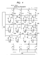
- FIG. 4 shows a circuit configuration example of an amplification solid state image pick-up device.
- the amplification solid state image pick-up device includes at least in a unit pixel: a photodiode; and an amplifying transistor that amplifies light signals accumulated in the photodiode.
- the unit pixels are arranged in a two-dimensional array.
- FIG. 5 is a plan view showing a pixel structure in a unit cell in a conventional amplification MOS sensor.
- reference numeral 2101 denotes a photodiode for photoelectric conversion
- 2102 a reset transistor for resetting the photodiode 2101 and a floating diffusion (FD) region 2106
- 2103 a transfer MOS transistor for transferring (reading out) signal charges in the photodiode 2101
- 2104 a source follower amplifier for converting the transferred (read-out) charges into a voltage, with its gate electrode connected to the FD region 2106 ;
- 2105 a row selection MOS transistor that connects an output of the source follower amplifier to a signal line.
- the FD region 2106 is constituted of an L-shaped diffusion layer in order to minimize its capacitance value C FD , in order to improve a charge-voltage conversion efficiency.
- a depletion layer region 2208 is formed between the FD region 2106 constituted of an n + layer and a p-type substrate.
- FIG. 6 is a plan view of a unit cell of a solid state image pick-up device disclosed in JP H10-150182 A.
- gate wirings 23 and 24 of a readout transistor are not discrete for each pixel and are not arranged close to a drain 25 of the readout transistor.
- the transfer MOS transistor 2103 of the transistors in FIG. 5 is an NMOS transistor, and has a gate electrode formed of a material including N-type polycrystalline silicon.
- FIG. 7 is a sectional view taken along the line 7 — 7 of FIG. 5 .
- reference numeral 2201 denotes an N-type silicon substrate; 2202 , a P-type well; 2203 , a P + type channel stop layer that is formed below a local-oxidation-of-silicon (LOCOS) oxide film 2204 in a self-aligned manner; 2205 , an N + type diffusion layer that constitutes part of the FD region 2106 ; 2206 , a gate electrode that is formed of high-concentration N-type polysilicon or silicide thereof; and 2207 , a gate insulating film of the transfer MOS transistor 2103 .
- LOC local-oxidation-of-silicon
- the circuit is shifted from a state where the reset MOS transistor 2102 is turned ON to a state where the transfer MOS transistor 2103 is turned ON for resetting the photodiode 2101 of FIG. 8 .
- the transfer MOS transistor 2103 is turned OFF to reset the photodiode 2101 .
- the photodiode in the reset state is then put into a charge accumulating state.
- the reset MOS transistor 2102 is turned OFF and the row selection MOS transistor 2105 is turned ON.
- the source follower amplifier 2104 is activated.
- the transfer MOS transistor 2103 is turned ON again, thereby to transfer signal charges in the photo diode 2101 to the FD region 2106 .
- a potential change corresponding to the transferred signal charges appears in the time chart of FD
- a voltage value of the vertical output line 2108 at the time of transferring the signal charges to the FD region 2106 is input (written) to a signal readout storage capacitor (Cts) 2110 by turning ON a transfer transistor 2111 .
- the transfer transistor 2111 is turned OFF.
- a differential amplifier, etc. (not shown) are used for generating a voltage corresponding to a difference between the output charge of the storage capacitor Cts and that of the storage capacitor Ctn. This makes it possible to eliminate noise generated at the reset time of the reset MOS transistor 2102 of the pixel or variation in threshold voltage of the source follower amplifier 2104 .
- a leak current is more likely to flow between the FD region and the substrate. If the leak current is generated in this portion, as indicated by the dotted line in the time chart of FD of FIG. 9 , the voltage of the FD region changes. As a result, the voltage values input (written) to the storage capacitors Ctn and Cts are different from the original (correct) ones, leading to a deterioration in image quality.
- this publication has no description about an influence that may be exerted on how the depletion layer spreads by a concentration of a semiconductor layer close to the drain 25 or a concentration of a semiconductor region just below the gate wirings 23 , 24 but excluding a channel formation region, or a work function of a material for each gate wiring.
- a difference in work function between the gate electrode and the semiconductor region just below the gate wirings 23 , 24 but excluding the channel formation region takes a positive value or zero, as explained below, even if the channel stop is disposed close to the FD region, a leak current will not increase. Accordingly, the use of a structure of the present invention provides not noticeable but substantial advantage at least rather than the prior art.
- a photoelectric conversion apparatus has a photodiode for converting light into a signal charge, a first semiconductor region having a first conductivity type, and a floating diffusion region formed from a second semiconductor region having a second conductivity type for converting the signal charge generated by the photodiode into a signal voltage, the second semiconductor region being formed in the first semiconductor region.
- the apparatus also comprises a depletion region formed in a border area between the first semiconductor region and the floating diffusion region, and an electrode is formed above the first semiconductor region and spaced from the first semiconductor region by an interposed insulating film, to increase the concentration of majority carriers in the first semiconductor region.
- an isolation region disposed in the periphery of the photodiode, the electrode extending to overlap with the isolation region, and a third semiconductor region of the first conductivity type disposed beneath the isolation region.
- the impurity concentration of the third semiconductor region is higher than that of the semiconductor region, and in addition, the electrode on the isolation region extends above at least part of the third semiconductor region, but does not extend above the depletion region.
- a photoelectric conversion apparatus comprises a plurality of pixels, each pixel of which comprises a first semiconductor region of a first conductivity type, a photodiode provided with a second semiconductor region of a second conductivity type disposed in the first semiconductor region for converting light into electron charge, and a transfer transistor for transfer the electron charge from the photodiode. Also provided are a third semiconductor region of the second conductivity type to which the electron charge from the photodiode is transferred through the transfer transistor, and an isolation region disposed in the periphery of the photodiode.
- the transfer transistor has a gate electrode that extends so as to overlap with the isolation region.
- a fourth semiconductor region of the first conductivity type disposed beneath the isolation region, the impurity concentration of the fourth semiconductor region being higher than that of the first semiconductor region.
- the gate electrode of the transfer transistor (which is discrete for every pixel) extends above at least part of the fourth semiconductor region with the isolation region interposed therebetween, and the third semiconductor region is formed adjacent to the gate electrode of the transfer transistor, but does not extend to be adjacent to a laminated portion of the fourth semiconductor region, the isolation region and the gate electrode.
- a photoelectric conversion apparatus comprising a plurality of pixels, where each pixel comprises a first semiconductor region of a first conductivity type, a photodiode provided with a second semiconductor region of a second conductivity type disposed in the first semiconductor region for converting light into electron charge, and a transfer transistor for transfer the electron charge from the photodiode.
- a third semiconductor region of the second conductivity type receives the electron charge from the photodiode when the charge is transferred through the transfer transistor.
- an isolation region is disposed in the periphery of the photodiode, a gate electrode of the transfer transistor extending to overlap with the isolation region.
- a fourth semiconductor region of the first conductivity type is disposed beneath the isolation region, and has an impurity concentration higher than that of the first semiconductor region.
- the gate electrode of the transfer transistor (which again is discrete for each pixel) extends above at least part of the fourth semiconductor region with the isolation region interposed therebetween, the pixel includes two laminated portions of the fourth semiconductor region, the isolation region and the gate electrode, and the width of the third semiconductor region in a side adjacent to the gate electrode is equal to or shorter than the distance between the two laminated portions.
- the present invention can provide a photoelectric conversion apparatus capable of reducing a leak current in a floating diffusion region with a high S/N ratio, and a solid state image pick-up apparatus using the same.
- FIG. 1 is a plan view showing a photoelectric conversion apparatus according to an embodiment of the present invention
- FIG. 2 is a sectional view taken along the line A-B-C-D of FIG. 1 , which shows the photoelectric conversion apparatus according to the embodiment of the present invention
- FIG. 3 is a block diagram showing a structure of an image pick-up apparatus according to an embodiment of the present invention.
- FIG. 4 is a plan view showing a circuit configuration example of an amplification solid state image pick-up device
- FIG. 5 is a plan view showing a conventional photoelectric conversion apparatus
- FIG. 6 is a plan view showing another conventional photoelectric conversion apparatus
- FIG. 7 is a sectional view taken along the line 7 — 7 of FIG. 5 , which shows the conventional photoelectric conversion apparatus;
- FIG. 8 is a circuit diagram showing an equivalent circuit of a photoelectric conversion apparatus.
- FIG. 9 is a timing chart showing operations of a photoelectric conversion apparatus.
- FIG. 1 is a plan view showing a photoelectric conversion apparatus according to Embodiment 1 of the present invention.
- reference numeral 101 denotes a photo diode for photoelectrical conversion
- 102 a reset transistor for resetting the photodiode 101 and a floating diffusion (FD) region 106
- 103 a transfer MOS transistor for transferring (reading out) signal charges in the photodiode 101
- 104 a source follower amplifier for converting the transferred (read-out) charges into a voltage, which has a gate electrode connected to the FD region 106 ;
- 105 a row selection MOS transistor that connects an output of the source follower amplifier to a signal line.
- FIG. 2 is a sectional view taken along the line A-B-C-D of FIG. 1 .
- reference numeral 201 denotes an N-type silicon substrate; 202 , a P-type well; 203 , a P + type channel stop layer formed below a local-oxidation-of-silicon (LOCOS) oxide film 204 in a self-aligned manner; 205 , an N + type diffusion layer that forms part of the FD region 106 ; and 206 , a gate electrode.
- the gate electrode 206 is formed of high-concentration N-type polysilicon or silicide thereof.
- Reference numeral 207 denotes a gate insulating film of the transfer MOS transistor 103 .
- Reference numeral 208 denotes a depletion layer constituted of the N + type diffusion layer 205 forming the FD region, the P-type well 202 , and the P + type channel stop layer.
- the mechanism of generating a leak current in the region is as follows. First, in a portion where the FD region 2205 , a high-concentration N + type layer, and the channel stop layer 2203 , a P + type layer, are formed close to each other, as for a voltage in the FD region 2205 , during an operation of reading out signals, a PN junction is reverse-biased in terms of operation since a positive voltage is applied to the P-type well 2202 . Also, the region includes a gate electrode 2206 made of N + type polysilicon and formed across a LOCOS oxide film from a P-type channel stop layer 2203 . The gate electrode 2206 and the P-type channel stop layer 2203 have a difference in work function therebetween.
- the channel stop layer 2203 effectively increases a concentration of majority carriers by the work function difference, thereby changing its conductivity type to P + .
- the region in a depletion layer 2208 formed between the FD region 2205 and the P-type well 2202 has a depletion layer width smaller than that of the region not including the gate electrode 2206 (that is, d 1 ⁇ d 2 ).
- a high electric field is applied between the N + type diffusion layer 2205 and the P + type channel stop layer 2203 , and thus a leak current is easily generated.
- N-type polysilicon or aluminum as a material having such a work function that causes majority carriers of a P-type region to effectively increase their concentration
- P-type polysilicon as a material having such a work function that causes majority carriers of an N-type region to effectively increase their concentration
- this phenomenon essentially occurs when a concentration of the majority carriers in the semiconductor region having an opposite conductivity type that forms the junction with the FD region to constitute the depletion layer is effectively increased as mentioned above. Therefore, for example, when a gate electrode potential of the transfer MOS transistor 103 close to the FD region or a gate potential of the reset MOS transistor 102 is negative one, a leak current is easily generated irrespective of a gate electrode material.
- the depletion layer width is shortened, leading to generation of a high electric field and increase in leak current in the FD region. Therefore, although not shown, even if no channel stop layer is formed, it is necessary not to form the electrode directly above the depletion layer derived from the FD region in arranging the above electrode. More specifically, the electrode needs to be formed 0.1 to 0.5 mm, preferably 0.2 to 0.4 mm apart from the FD region.
- JP H10-150182 A shows a case where a concentration of majority carrier in the channel stop is increased due to the work function difference so that an electric field in depletion layer (between the diffusion layer (FD region) and the channel stop) is strengthened and thus a leak current increases when a reverse bias is applied between the well region and diffusion region.
- the use of the structure shown in FIG. 2 according to the present invention, provides not noticeable but substantial advantage at least rather than the prior art.
- FIG. 3 shows a system configuration of an image pick-up apparatus using the photoelectric conversion apparatus of the above embodiment, as an image pick-up apparatus according to the present invention.
- an image pick-up apparatus includes: a barrier or shutter 1 serving as both a protector of a lens and a main switch thereof; a lens 2 for focusing an optical image of an object on a solid state image pick-up device 4 ; a diaphragm 3 for adjusting how much of the light that has passed through the lens 2 is allowed to reach the solid state image pick-up device 4 (corresponding to the photoelectric conversion apparatus as described in the above embodiment) for taking in the formed object image through the lens 2 as an image signal; a circuit 5 processing image pick-up signal for effecting various types of correction or clamping on the image signal output from the solid state image pick-up device 4 ; an A/D converter 6 for effecting analog-digital conversion on the image signal output from the solid state image pick-up device 4 ; a signal processor 7 for effecting various types of correction or data compression on image data
- a solid state image pick-up system is configured by an arithmetic operation unit controlling unit 9 for performing various arithmetic operations and controlling the whole still video camera; a memory 10 for temporarily storing image data; an interface (I/F) controlling a recording medium 11 for recording or reading out data on/from a recording medium; a removably insertable recording medium 12 for recording or reading out image data, such as a semiconductor memory; and an external interface (I/F) 13 for communicating with an external computer, etc.
- an arithmetic operation unit controlling unit 9 for performing various arithmetic operations and controlling the whole still video camera
- a memory 10 for temporarily storing image data
- an interface (I/F) controlling a recording medium 11 for recording or reading out data on/from a recording medium
- a removably insertable recording medium 12 for recording or reading out image data, such as a semiconductor memory
- an external interface (I/F) 13 for communicating with an external computer, etc.
- a main power source is turned ON, and then the control system is powered on, as is the image pick-up system circuit including the A/D converter 6 .
- the arithmetic operation unit controlling unit 9 opens the diaphragm 3 for controlling an exposure amount and signals output from the solid state image pick-up device 4 directly pass through the circuit 5 processing image pick-up signal to be output to the A/D converter 6 .
- the A/D converter 6 effects A/D conversion on the signals to be output to the signal processor 7 .
- the signal processor 7 calculates the exposure amount based on the input data with the arithmetic operation unit controlling unit 9 .
- Lightness is judged based on results of the exposure metering and the arithmetic operation unit controlling unit 9 controls the diaphragm according to the judgment result.
- a high-frequency component is extracted based on signals output from the solid state image pick-up device 4 and the arithmetic operation unit controlling unit 9 calculates a distance to an object.
- the lens 2 is driven, and a judgment is made a to whether or not focusing is obtained. If it is judged that the system is not focused, the lens 2 is driven again to measure the distance to the object.
- the main exposure starts.
- the image signals output from the solid state image pick-up device 4 undergo correction, etc., with the circuit 5 processing image pick-up signal and A/D conversion with the A/D converter 6 , and then pass through the signal processor 7 to be stored in the memory 10 with the arithmetic operation unit controlling whole 9 .
- data stored in the memory 10 is recorded on the removably insertable recording medium 12 such as a semiconductor memory, through the I/F controlling recording medium 11 under the control of the arithmetic operation unit controlling unit 9 .
- the data may be directly input to a computer, etc., through the external I/F 13 for image processing.
- the present invention can be used for taking an image.
Abstract
Description
Claims (6)
Priority Applications (1)
| Application Number | Priority Date | Filing Date | Title |
|---|---|---|---|
| US11/608,073 US7531885B2 (en) | 2003-11-10 | 2006-12-07 | Photoelectric conversion apparatus and image pick-up system using the photoelectric conversion apparatus |
Applications Claiming Priority (2)
| Application Number | Priority Date | Filing Date | Title |
|---|---|---|---|
| JP2003-380090 | 2003-11-10 | ||
| JP2003380090A JP4514188B2 (en) | 2003-11-10 | 2003-11-10 | Photoelectric conversion device and imaging device |
Related Child Applications (1)
| Application Number | Title | Priority Date | Filing Date |
|---|---|---|---|
| US11/608,073 Division US7531885B2 (en) | 2003-11-10 | 2006-12-07 | Photoelectric conversion apparatus and image pick-up system using the photoelectric conversion apparatus |
Publications (2)
| Publication Number | Publication Date |
|---|---|
| US20050098805A1 US20050098805A1 (en) | 2005-05-12 |
| US7187052B2 true US7187052B2 (en) | 2007-03-06 |
Family
ID=34544543
Family Applications (2)
| Application Number | Title | Priority Date | Filing Date |
|---|---|---|---|
| US10/971,151 Expired - Fee Related US7187052B2 (en) | 2003-11-10 | 2004-10-25 | Photoelectric conversion apparatus and image pick-up system using the photoelectric conversion apparatus |
| US11/608,073 Expired - Fee Related US7531885B2 (en) | 2003-11-10 | 2006-12-07 | Photoelectric conversion apparatus and image pick-up system using the photoelectric conversion apparatus |
Family Applications After (1)
| Application Number | Title | Priority Date | Filing Date |
|---|---|---|---|
| US11/608,073 Expired - Fee Related US7531885B2 (en) | 2003-11-10 | 2006-12-07 | Photoelectric conversion apparatus and image pick-up system using the photoelectric conversion apparatus |
Country Status (2)
| Country | Link |
|---|---|
| US (2) | US7187052B2 (en) |
| JP (1) | JP4514188B2 (en) |
Cited By (50)
| Publication number | Priority date | Publication date | Assignee | Title |
|---|---|---|---|---|
| US20060158543A1 (en) * | 2005-01-14 | 2006-07-20 | Canon Kabushiki Kaisha | Solid state image pickup device, camera, and driving method of solid state image pickup device |
| US20060157759A1 (en) * | 2005-01-14 | 2006-07-20 | Canon Kabushiki Kaisha | Image pickup device, its control method, and camera |
| US20060158539A1 (en) * | 2005-01-14 | 2006-07-20 | Canon Kabushiki Kaisha | Solid-state image pickup device and control method thereof, and camera |
| US20060208291A1 (en) * | 2005-03-18 | 2006-09-21 | Canon Kabushiki Kaisha | Solid state image pickup device and camera |
| US20060208161A1 (en) * | 2005-03-18 | 2006-09-21 | Canon Kabushiki Kaisha | Solid state image pickup device and camera |
| US20070085110A1 (en) * | 2003-11-10 | 2007-04-19 | Canon Kabushiki Kaisha | Photoelectric conversion apparatus and image pick-up system using the photoelectric conversion apparatus |
| US20070205439A1 (en) * | 2006-03-06 | 2007-09-06 | Canon Kabushiki Kaisha | Image pickup apparatus and image pickup system |
| US20080006892A1 (en) * | 2006-07-10 | 2008-01-10 | Canon Kabushiki Kaisha | Photoelectric conversion device and image pickup system with photoelectric conversion device |
| US20080024630A1 (en) * | 2006-07-26 | 2008-01-31 | Canon Kabushiki Kaisha | Photoelectric conversion device and image capturing device |
| US20080062294A1 (en) * | 2006-09-07 | 2008-03-13 | Canon Kabushiki Kaisha | Signal reading apparatus and image pickup system using the signal reading apparatus |
| US20080174688A1 (en) * | 2003-12-03 | 2008-07-24 | Canon Kabushiki Kaisha | Solid state image pickup device, method for producing the same, and image pickup system comprising the solid state image pickup device |
| US7408210B2 (en) | 2005-03-18 | 2008-08-05 | Canon Kabushiki Kaisha | Solid state image pickup device and camera |
| US20090033781A1 (en) * | 2007-08-02 | 2009-02-05 | Canon Kabushiki Kaisha | Image sensing apparatus and image capturing system |
| US20090085142A1 (en) * | 2005-01-05 | 2009-04-02 | Sony Corporation | Solid-state imaging device and method for fabricating same |
| US20090147117A1 (en) * | 2007-12-05 | 2009-06-11 | Canon Kabushiki Kaisha | Photoelectric conversion device and imaging system |
| US20090218477A1 (en) * | 2008-02-29 | 2009-09-03 | Canon Kabushiki Kaisha | Image sensing apparatus and image sensing system |
| US20090218479A1 (en) * | 2008-02-29 | 2009-09-03 | Canon Kabushiki Kaisha | Image sensing apparatus and imaging system |
| US20090237543A1 (en) * | 2008-03-19 | 2009-09-24 | Canon Kabushiki Kaisha | Solid-state image pickup apparatus |
| US20100060762A1 (en) * | 2008-09-10 | 2010-03-11 | Canon Kabushiki Kaisha | Photoelectric conversion apparatus and imaging system |
| US20100149394A1 (en) * | 2008-12-17 | 2010-06-17 | Canon Kabushiki Kaisha | Solid-state imaging apparatus and imaging system using the solid-state imaging apparatus |
| US20100182465A1 (en) * | 2009-01-21 | 2010-07-22 | Canon Kabushiki Kaisha | Solid-state imaging apparatus |
| US20110068252A1 (en) * | 2009-09-24 | 2011-03-24 | Canon Kabushiki Kaisha | Photoelectric conversion apparatus and imaging system using the same |
| US20110068253A1 (en) * | 2009-09-24 | 2011-03-24 | Canon Kabushiki Kaisha | Photoelectric conversion apparatus and imaging system using the photoelectric conversion apparatus |
| US8208055B2 (en) | 2008-03-27 | 2012-06-26 | Canon Kabushiki Kaisha | Solid-state imaging apparatus and imaging system |
| US8218050B2 (en) | 2008-02-28 | 2012-07-10 | Canon Kabushiki Kaisha | Solid-state imaging apparatus, method of driving solid-state imaging apparatus, and imaging system |
| US8598901B2 (en) | 2011-10-07 | 2013-12-03 | Canon Kabushiki Kaisha | Photoelectric conversion system |
| US8711259B2 (en) | 2011-10-07 | 2014-04-29 | Canon Kabushiki Kaisha | Solid-state imaging apparatus |
| US8836838B2 (en) | 2011-09-05 | 2014-09-16 | Canon Kabushiki Kaisha | Solid-state imaging apparatus and method of driving the same |
| US8928786B2 (en) | 2011-10-07 | 2015-01-06 | Canon Kabushiki Kaisha | Solid-state imaging apparatus and method of driving the same |
| US9029752B2 (en) | 2011-07-28 | 2015-05-12 | Canon Kabushiki Kaisha | Solid state imaging apparatus including reference signal generator with a slope converting circuit |
| US9053996B2 (en) | 2012-02-29 | 2015-06-09 | Canon Kabushiki Kaisha | Solid-state imaging apparatus with a plurality of processing portions |
| US9147708B2 (en) | 2012-01-18 | 2015-09-29 | Canon Kabushiki Kaisha | Solid-state image sensor and camera |
| US9232165B2 (en) | 2011-09-08 | 2016-01-05 | Canon Kabushiki Kaisha | Solid-state imaging apparatus and method for driving solid-state imaging apparatus |
| US9270913B2 (en) | 2013-04-25 | 2016-02-23 | Canon Kabushiki Kaisha | Photoelectric conversion apparatus and imaging system |
| US9288415B2 (en) | 2013-09-17 | 2016-03-15 | Canon Kabushiki Kaisha | Solid-state imaging apparatus and imaging system |
| US9300884B2 (en) | 2011-10-03 | 2016-03-29 | Canon Kabushiki Kaisha | Solid-state image sensor and camera having a plurality of photoelectric converters under a microlens |
| US9438839B2 (en) | 2013-12-27 | 2016-09-06 | Canon Kabushiki Kaisha | Solid state imaging apparatus and imaging system using the same |
| US9497403B2 (en) | 2013-05-10 | 2016-11-15 | Canon Kabushiki Kaisha | Solid-state imaging apparatus and camera |
| US9509931B2 (en) | 2014-04-01 | 2016-11-29 | Canon Kabushiki Kaisha | Solid-state imaging apparatus and camera |
| US9549139B2 (en) | 2013-08-28 | 2017-01-17 | Canon Kabushiki Kaisha | Imaging apparatus, imaging system, and method for driving imaging apparatus |
| US9942497B2 (en) | 2013-04-18 | 2018-04-10 | Canon Kabushiki Kaisha | Solid-state imaging apparatus and imaging with a limiting circuit for limiting an amplifier output in first and second periods to first and second ranges |
| US9948877B2 (en) | 2014-08-20 | 2018-04-17 | Canon Kabushiki Kaisha | Solid-state imaging apparatus and imaging system having first and second metal members arranged in different directions |
| US9979916B2 (en) | 2014-11-21 | 2018-05-22 | Canon Kabushiki Kaisha | Imaging apparatus and imaging system |
| US10319765B2 (en) | 2016-07-01 | 2019-06-11 | Canon Kabushiki Kaisha | Imaging device having an effective pixel region, an optical black region and a dummy region each with pixels including a photoelectric converter |
| US10347679B2 (en) | 2016-05-26 | 2019-07-09 | Canon Kabushiki Kaisha | Imaging device |
| US10382707B2 (en) | 2016-11-15 | 2019-08-13 | Canon Kabushiki Kaisha | Imaging device |
| US10992886B2 (en) | 2018-09-10 | 2021-04-27 | Canon Kabushiki Kaisha | Solid state imaging device, imaging system, and drive method of solid state imaging device |
| US11310453B2 (en) | 2018-12-06 | 2022-04-19 | Canon Kabushiki Kaisha | Photoelectric conversion device and imaging system |
| US11336844B2 (en) | 2018-08-23 | 2022-05-17 | Canon Kabushiki Kaisha | Imaging device, imaging system, and movable object |
| US11425365B2 (en) | 2018-12-14 | 2022-08-23 | Canon Kabushiki Kaisha | Photoelectric conversion device, method of manufacturing photoelectric conversion device, and method of manufacturing semiconductor device |
Families Citing this family (18)
| Publication number | Priority date | Publication date | Assignee | Title |
|---|---|---|---|---|
| JP3793202B2 (en) * | 2004-02-02 | 2006-07-05 | キヤノン株式会社 | Solid-state imaging device |
| JP3890333B2 (en) * | 2004-02-06 | 2007-03-07 | キヤノン株式会社 | Solid-state imaging device |
| JP4067054B2 (en) * | 2004-02-13 | 2008-03-26 | キヤノン株式会社 | Solid-state imaging device and imaging system |
| US7294818B2 (en) * | 2004-08-24 | 2007-11-13 | Canon Kabushiki Kaisha | Solid state image pickup device and image pickup system comprising it |
| JP2006073736A (en) * | 2004-09-01 | 2006-03-16 | Canon Inc | Photoelectric converter, solid state imaging device and system |
| JP4916101B2 (en) * | 2004-09-01 | 2012-04-11 | キヤノン株式会社 | Photoelectric conversion device, solid-state imaging device, and solid-state imaging system |
| JP4971586B2 (en) | 2004-09-01 | 2012-07-11 | キヤノン株式会社 | Solid-state imaging device |
| JP5089017B2 (en) * | 2004-09-01 | 2012-12-05 | キヤノン株式会社 | Solid-state imaging device and solid-state imaging system |
| JP4794877B2 (en) * | 2005-03-18 | 2011-10-19 | キヤノン株式会社 | Solid-state imaging device and camera |
| JP2007035674A (en) * | 2005-07-22 | 2007-02-08 | Nikon Corp | Solid state imaging device |
| US7833819B2 (en) * | 2008-07-23 | 2010-11-16 | Aptina Imaging Corporation | Method and apparatus for decreasing storage node parasitic charge in active pixel image sensors |
| JP5688540B2 (en) * | 2010-02-26 | 2015-03-25 | パナソニックIpマネジメント株式会社 | Solid-state imaging device and camera |
| JP5651982B2 (en) | 2010-03-31 | 2015-01-14 | ソニー株式会社 | Solid-state imaging device, method for manufacturing solid-state imaging device, and electronic apparatus |
| US8294077B2 (en) * | 2010-12-17 | 2012-10-23 | Omnivision Technologies, Inc. | Image sensor having supplemental capacitive coupling node |
| JP2012182377A (en) * | 2011-03-02 | 2012-09-20 | Sony Corp | Solid-state imaging device |
| JP2015023117A (en) * | 2013-07-18 | 2015-02-02 | 株式会社ニコン | Solid-state imaging element, and imaging device |
| US9443758B2 (en) | 2013-12-11 | 2016-09-13 | Taiwan Semiconductor Manufacturing Co., Ltd. | Connecting techniques for stacked CMOS devices |
| US9787928B2 (en) * | 2015-01-06 | 2017-10-10 | Forza Silicon Corporation | Layout and timing schemes for ping-pong readout architecture |
Citations (12)
| Publication number | Priority date | Publication date | Assignee | Title |
|---|---|---|---|---|
| JPH10150182A (en) | 1996-09-19 | 1998-06-02 | Toshiba Corp | Solid-state image sensing device and solid-state image sensing device application system |
| US6188094B1 (en) | 1998-03-19 | 2001-02-13 | Canon Kabushiki Kaisha | Solid-state image pickup device |
| US20020079518A1 (en) | 2000-12-22 | 2002-06-27 | Mitsubishi Denki Kabushiki Kaisha | Solid imaging device and production method thereof |
| US6423993B1 (en) | 1999-02-09 | 2002-07-23 | Sony Corporation | Solid-state image-sensing device and method for producing the same |
| JP2002353430A (en) | 2001-05-22 | 2002-12-06 | Canon Inc | Photoelectric transducer and imaging device |
| JP2003087663A (en) | 2001-06-28 | 2003-03-20 | Victor Co Of Japan Ltd | Solid-state imaging apparatus |
| US20030160295A1 (en) | 2002-02-28 | 2003-08-28 | Canon Kabushiki Kaisha | Semiconductor device, image pickup device using the same, and photoelectric conversion device |
| US20030164887A1 (en) | 2002-02-27 | 2003-09-04 | Canon Kabushiki Kaisha | Signal processing device and image pickup apparatus using the same |
| US20030218117A1 (en) | 2002-02-27 | 2003-11-27 | Canon Kabushiki Kaisha | Photoelectric conversion device |
| US6670990B1 (en) | 1997-09-29 | 2003-12-30 | Canon Kabushiki Kaisha | Image sensing device using MOS-type image sensing element whose threshold voltage of charge transfer switch and reset switch is different from that of signal output transistor |
| US6674470B1 (en) | 1996-09-19 | 2004-01-06 | Kabushiki Kaisha Toshiba | MOS-type solid state imaging device with high sensitivity |
| US20050176167A1 (en) * | 2002-12-27 | 2005-08-11 | Hynix Semiconductor Inc. | Method for fabricating image sensor including isolation layer having trench structure |
Family Cites Families (6)
| Publication number | Priority date | Publication date | Assignee | Title |
|---|---|---|---|---|
| JPS62277764A (en) * | 1986-05-26 | 1987-12-02 | Mitsubishi Electric Corp | Solid-state image sensing element |
| JPH11261046A (en) | 1998-03-12 | 1999-09-24 | Canon Inc | Solid-state image pickup device |
| JP2001196572A (en) * | 2000-01-13 | 2001-07-19 | Canon Inc | Photoelectric conversion device |
| JP4514188B2 (en) * | 2003-11-10 | 2010-07-28 | キヤノン株式会社 | Photoelectric conversion device and imaging device |
| JP4508619B2 (en) | 2003-12-03 | 2010-07-21 | キヤノン株式会社 | Method for manufacturing solid-state imaging device |
| KR100560389B1 (en) | 2004-07-05 | 2006-03-13 | 한국전자통신연구원 | Optimal Base Station Selecting Method in Wireless Network |
-
2003
- 2003-11-10 JP JP2003380090A patent/JP4514188B2/en not_active Expired - Fee Related
-
2004
- 2004-10-25 US US10/971,151 patent/US7187052B2/en not_active Expired - Fee Related
-
2006
- 2006-12-07 US US11/608,073 patent/US7531885B2/en not_active Expired - Fee Related
Patent Citations (17)
| Publication number | Priority date | Publication date | Assignee | Title |
|---|---|---|---|---|
| US6674470B1 (en) | 1996-09-19 | 2004-01-06 | Kabushiki Kaisha Toshiba | MOS-type solid state imaging device with high sensitivity |
| JPH10150182A (en) | 1996-09-19 | 1998-06-02 | Toshiba Corp | Solid-state image sensing device and solid-state image sensing device application system |
| US6670990B1 (en) | 1997-09-29 | 2003-12-30 | Canon Kabushiki Kaisha | Image sensing device using MOS-type image sensing element whose threshold voltage of charge transfer switch and reset switch is different from that of signal output transistor |
| US6605850B1 (en) | 1998-03-19 | 2003-08-12 | Canon Kabushiki Kaisha | Solid-state image pickup device using layers having different refractive indices |
| US6188094B1 (en) | 1998-03-19 | 2001-02-13 | Canon Kabushiki Kaisha | Solid-state image pickup device |
| US6423993B1 (en) | 1999-02-09 | 2002-07-23 | Sony Corporation | Solid-state image-sensing device and method for producing the same |
| US6492668B2 (en) | 2000-12-22 | 2002-12-10 | Mitsubishi Denki Kabushiki Kaisha | Solid imaging device and production method thereof |
| JP2002190586A (en) | 2000-12-22 | 2002-07-05 | Mitsubishi Electric Corp | Solid-state image pickup device and method of manufacturing the same |
| US20020079518A1 (en) | 2000-12-22 | 2002-06-27 | Mitsubishi Denki Kabushiki Kaisha | Solid imaging device and production method thereof |
| JP2002353430A (en) | 2001-05-22 | 2002-12-06 | Canon Inc | Photoelectric transducer and imaging device |
| JP2003087663A (en) | 2001-06-28 | 2003-03-20 | Victor Co Of Japan Ltd | Solid-state imaging apparatus |
| US20030164887A1 (en) | 2002-02-27 | 2003-09-04 | Canon Kabushiki Kaisha | Signal processing device and image pickup apparatus using the same |
| US20030218117A1 (en) | 2002-02-27 | 2003-11-27 | Canon Kabushiki Kaisha | Photoelectric conversion device |
| US20030160295A1 (en) | 2002-02-28 | 2003-08-28 | Canon Kabushiki Kaisha | Semiconductor device, image pickup device using the same, and photoelectric conversion device |
| JP2003258229A (en) | 2002-02-28 | 2003-09-12 | Canon Inc | Semiconductor device, photoelectric converter and imaging device |
| US6774453B2 (en) | 2002-02-28 | 2004-08-10 | Canon Kabushiki Kaisha | Semiconductor device, image pickup device using the same, and photoelectric conversion device |
| US20050176167A1 (en) * | 2002-12-27 | 2005-08-11 | Hynix Semiconductor Inc. | Method for fabricating image sensor including isolation layer having trench structure |
Cited By (103)
| Publication number | Priority date | Publication date | Assignee | Title |
|---|---|---|---|---|
| US20070085110A1 (en) * | 2003-11-10 | 2007-04-19 | Canon Kabushiki Kaisha | Photoelectric conversion apparatus and image pick-up system using the photoelectric conversion apparatus |
| US7531885B2 (en) * | 2003-11-10 | 2009-05-12 | Canon Kabushiki Kaisha | Photoelectric conversion apparatus and image pick-up system using the photoelectric conversion apparatus |
| US20080174688A1 (en) * | 2003-12-03 | 2008-07-24 | Canon Kabushiki Kaisha | Solid state image pickup device, method for producing the same, and image pickup system comprising the solid state image pickup device |
| US7646493B2 (en) | 2003-12-03 | 2010-01-12 | Canon Kabushiki Kaisha | Solid state image pickup device, method for producing the same, and image pickup system comprising the solid state image pickup device |
| US20090085142A1 (en) * | 2005-01-05 | 2009-04-02 | Sony Corporation | Solid-state imaging device and method for fabricating same |
| US8421894B2 (en) | 2005-01-14 | 2013-04-16 | Canon Kabushiki Kaisha | Solid-state image pickup device and control method thereof, and camera |
| US8089545B2 (en) | 2005-01-14 | 2012-01-03 | Canon Kabushiki Kaisha | Solid-state image pickup device and control method thereof, and camera |
| US20110074993A1 (en) * | 2005-01-14 | 2011-03-31 | Canon Kabushiki Kaisha | Image pickup device, its control method, and camera |
| US7872286B2 (en) | 2005-01-14 | 2011-01-18 | Canon Kabushiki Kaisha | Image pickup device, its control method, and camera |
| US7466003B2 (en) | 2005-01-14 | 2008-12-16 | Canon Kabushiki Kaisha | Solid state image pickup device, camera, and driving method of solid state image pickup device |
| US8883526B2 (en) | 2005-01-14 | 2014-11-11 | Canon Kabushiki Kaisha | Image pickup device, its control method, and camera |
| US20090213260A1 (en) * | 2005-01-14 | 2009-08-27 | Canon Kabushiki Kaisha | Solid-state image pickup device and control method thereof, and camera |
| US20060158543A1 (en) * | 2005-01-14 | 2006-07-20 | Canon Kabushiki Kaisha | Solid state image pickup device, camera, and driving method of solid state image pickup device |
| US7538810B2 (en) | 2005-01-14 | 2009-05-26 | Canon Kabushiki Kaisha | Solid-state image pickup device and control method thereof, and camera |
| US20060158539A1 (en) * | 2005-01-14 | 2006-07-20 | Canon Kabushiki Kaisha | Solid-state image pickup device and control method thereof, and camera |
| US20060157759A1 (en) * | 2005-01-14 | 2006-07-20 | Canon Kabushiki Kaisha | Image pickup device, its control method, and camera |
| US8896029B2 (en) | 2005-03-18 | 2014-11-25 | Canon Kabushiki Kaisha | Solid state image pickup device and camera |
| US20060208161A1 (en) * | 2005-03-18 | 2006-09-21 | Canon Kabushiki Kaisha | Solid state image pickup device and camera |
| US7321110B2 (en) | 2005-03-18 | 2008-01-22 | Canon Kabushiki Kaisha | Solid state image pickup device and camera |
| US7460162B2 (en) * | 2005-03-18 | 2008-12-02 | Canon Kabushiki Kaisha | Solid state image pickup device and camera |
| US8063958B2 (en) | 2005-03-18 | 2011-11-22 | Canon Kabushiki Kaisha | Solid state image pickup device with first and second photoelectric conversion regions and carrier accumulating units connected in parallel to each input portion of plural amplifying units |
| US7408210B2 (en) | 2005-03-18 | 2008-08-05 | Canon Kabushiki Kaisha | Solid state image pickup device and camera |
| US20060208291A1 (en) * | 2005-03-18 | 2006-09-21 | Canon Kabushiki Kaisha | Solid state image pickup device and camera |
| US20080068480A1 (en) * | 2005-03-18 | 2008-03-20 | Canon Kabushiki Kaisha | Solid state image pickup device and camera |
| US8390708B2 (en) | 2005-03-18 | 2013-03-05 | Canon Kabushiki Kaisha | Solid state image pickup device and camera utilizing carrier holding unit and floating diffusion region |
| US8441558B2 (en) | 2005-03-18 | 2013-05-14 | Canon Kabushiki Kaisha | Solid state image pickup device and camera having arrayed pixels including amplifying units |
| US7978241B2 (en) | 2005-03-18 | 2011-07-12 | Canon Kabushiki Kaisha | Solid state image pickup device and camera which can prevent color mixture |
| US20110157441A1 (en) * | 2005-03-18 | 2011-06-30 | Canon Kabushiki Kaisha | Solid state image pickup device and camera |
| US8698935B2 (en) | 2005-03-18 | 2014-04-15 | Canon Kabushiki Kaisha | Solid-state image pickup device and camera having arrayed pixels including amplifying units |
| US8749675B2 (en) | 2005-03-18 | 2014-06-10 | Canon Kabushiki Kaisha | Solid state image pickup device and camera which can prevent color mixture |
| US20070205439A1 (en) * | 2006-03-06 | 2007-09-06 | Canon Kabushiki Kaisha | Image pickup apparatus and image pickup system |
| US7749790B2 (en) | 2006-07-10 | 2010-07-06 | Canon Kabushiki Kaisha | Photoelectric conversion device and image pickup system with photoelectric conversion device |
| US20080006892A1 (en) * | 2006-07-10 | 2008-01-10 | Canon Kabushiki Kaisha | Photoelectric conversion device and image pickup system with photoelectric conversion device |
| US7459760B2 (en) | 2006-07-10 | 2008-12-02 | Canon Kabushiki Kaisha | Photoelectric conversion device and image pickup system with photoelectric conversion device |
| US20090053849A1 (en) * | 2006-07-10 | 2009-02-26 | Canon Kabushiski Kaisha | Photoelectric conversion device and image pickup system with photoelectric conversion device |
| US20080024630A1 (en) * | 2006-07-26 | 2008-01-31 | Canon Kabushiki Kaisha | Photoelectric conversion device and image capturing device |
| US20100314530A1 (en) * | 2006-07-26 | 2010-12-16 | Canon Kabushiki Kaisha | Photoelectric conversion device and image capturing device |
| US7812876B2 (en) | 2006-07-26 | 2010-10-12 | Canon Kabushiki Kaisha | Photoelectric conversion device and image capturing device with variable amplifier for amplifying signal by a selected gain |
| US8823849B2 (en) | 2006-07-26 | 2014-09-02 | Canon Kabushiki Kaisha | Photoelectric conversion device and image capturing device having circuit for reducing offset generated by amplifiers |
| US20080062294A1 (en) * | 2006-09-07 | 2008-03-13 | Canon Kabushiki Kaisha | Signal reading apparatus and image pickup system using the signal reading apparatus |
| US7948541B2 (en) | 2006-09-07 | 2011-05-24 | Canon Kabushiki Kaisha | Signal reading apparatus and image pickup system using the signal reading apparatus |
| US20110194005A1 (en) * | 2006-09-07 | 2011-08-11 | Canon Kabushiki Kaisha | Signal reading apparatus and image pickup system using the signal reading apparatus |
| US8797435B2 (en) | 2006-09-07 | 2014-08-05 | Canon Kabushiki Kaisha | Signal reading apparatus and image pickup system using the signal reading apparatus |
| US8009213B2 (en) | 2007-08-02 | 2011-08-30 | Canon Kabushiki Kaisha | Image sensing apparatus and image capturing system |
| US8427567B2 (en) | 2007-08-02 | 2013-04-23 | Canon Kabushiki Kaisha | Image sensing apparatus and image capturing system |
| US20090033781A1 (en) * | 2007-08-02 | 2009-02-05 | Canon Kabushiki Kaisha | Image sensing apparatus and image capturing system |
| US8159573B2 (en) | 2007-12-05 | 2012-04-17 | Canon Kabushiki Kaisha | Photoelectric conversion device and imaging system |
| US20090147117A1 (en) * | 2007-12-05 | 2009-06-11 | Canon Kabushiki Kaisha | Photoelectric conversion device and imaging system |
| US8218050B2 (en) | 2008-02-28 | 2012-07-10 | Canon Kabushiki Kaisha | Solid-state imaging apparatus, method of driving solid-state imaging apparatus, and imaging system |
| US8278613B2 (en) | 2008-02-29 | 2012-10-02 | Canon Kabushiki Kaisha | Image sensing apparatus and image sensing system |
| US20090218477A1 (en) * | 2008-02-29 | 2009-09-03 | Canon Kabushiki Kaisha | Image sensing apparatus and image sensing system |
| US20090218479A1 (en) * | 2008-02-29 | 2009-09-03 | Canon Kabushiki Kaisha | Image sensing apparatus and imaging system |
| US8106343B2 (en) | 2008-02-29 | 2012-01-31 | Canon Kabushiki Kaisha | Image sensing system interposing light shielding portion between color filter and pixel arrays |
| US8120686B2 (en) | 2008-03-19 | 2012-02-21 | Canon Kabushiki Kaisha | Solid-state image pickup apparatus |
| US20090237543A1 (en) * | 2008-03-19 | 2009-09-24 | Canon Kabushiki Kaisha | Solid-state image pickup apparatus |
| US8427565B2 (en) | 2008-03-27 | 2013-04-23 | Canon Kabushiki Kaisha | Solid-state imaging apparatus and imaging system |
| US8208055B2 (en) | 2008-03-27 | 2012-06-26 | Canon Kabushiki Kaisha | Solid-state imaging apparatus and imaging system |
| US8493487B2 (en) | 2008-09-10 | 2013-07-23 | Canon Kabushiki Kaisha | Photoelectric conversion apparatus and imaging system using floating light shielding portions |
| US20100060762A1 (en) * | 2008-09-10 | 2010-03-11 | Canon Kabushiki Kaisha | Photoelectric conversion apparatus and imaging system |
| US8325260B2 (en) | 2008-12-17 | 2012-12-04 | Canon Kabushiki Kaisha | Solid-state imaging apparatus including pixel matrix with selectable blocks of output lines and imaging system using the solid-state imaging apparatus |
| US20100149394A1 (en) * | 2008-12-17 | 2010-06-17 | Canon Kabushiki Kaisha | Solid-state imaging apparatus and imaging system using the solid-state imaging apparatus |
| US8810706B2 (en) | 2008-12-17 | 2014-08-19 | Canon Kabushiki Kaisha | Solid-state imaging apparatus and imaging system using the solid-state imaging apparatus |
| US9214491B2 (en) | 2009-01-21 | 2015-12-15 | Canon Kabushiki Kaisha | Solid-state imaging apparatus for causing an FD capacitor value to be variable without increasing a number of elements |
| US8913166B2 (en) | 2009-01-21 | 2014-12-16 | Canon Kabushiki Kaisha | Solid-state imaging apparatus |
| US20100182465A1 (en) * | 2009-01-21 | 2010-07-22 | Canon Kabushiki Kaisha | Solid-state imaging apparatus |
| US8466401B2 (en) | 2009-09-24 | 2013-06-18 | Canon Kabushiki Kaisha | Photoelectric conversion apparatus and imaging system using the photoelectric conversion apparatus |
| US8796609B2 (en) | 2009-09-24 | 2014-08-05 | Canon Kabushiki Kaisha | Photoelectric conversion apparatus and imaging system using the photoelectric conversion apparatus |
| US8519316B2 (en) | 2009-09-24 | 2013-08-27 | Canon Kabushiki Kaisha | Photoelectric conversion apparatus and imaging system using the same |
| US9040895B2 (en) | 2009-09-24 | 2015-05-26 | Canon Kabushiki Kaisha | Photoelectric conversion apparatus and imaging system using the same |
| US20110068252A1 (en) * | 2009-09-24 | 2011-03-24 | Canon Kabushiki Kaisha | Photoelectric conversion apparatus and imaging system using the same |
| US20110068253A1 (en) * | 2009-09-24 | 2011-03-24 | Canon Kabushiki Kaisha | Photoelectric conversion apparatus and imaging system using the photoelectric conversion apparatus |
| US9029752B2 (en) | 2011-07-28 | 2015-05-12 | Canon Kabushiki Kaisha | Solid state imaging apparatus including reference signal generator with a slope converting circuit |
| US8836838B2 (en) | 2011-09-05 | 2014-09-16 | Canon Kabushiki Kaisha | Solid-state imaging apparatus and method of driving the same |
| US9232165B2 (en) | 2011-09-08 | 2016-01-05 | Canon Kabushiki Kaisha | Solid-state imaging apparatus and method for driving solid-state imaging apparatus |
| US9773827B2 (en) | 2011-10-03 | 2017-09-26 | Canon Kabushiki Kaisha | Solid-state image sensor and camera where the plurality of pixels form a pixel group under a single microlens |
| US9300884B2 (en) | 2011-10-03 | 2016-03-29 | Canon Kabushiki Kaisha | Solid-state image sensor and camera having a plurality of photoelectric converters under a microlens |
| US10504947B2 (en) | 2011-10-03 | 2019-12-10 | Canon Kabushiki Kaisha | Solid-state image sensor and camera |
| US11348953B2 (en) | 2011-10-03 | 2022-05-31 | Canon Kabushiki Kaisha | Solid-state image sensor and camera |
| US8598901B2 (en) | 2011-10-07 | 2013-12-03 | Canon Kabushiki Kaisha | Photoelectric conversion system |
| US8928786B2 (en) | 2011-10-07 | 2015-01-06 | Canon Kabushiki Kaisha | Solid-state imaging apparatus and method of driving the same |
| US8711259B2 (en) | 2011-10-07 | 2014-04-29 | Canon Kabushiki Kaisha | Solid-state imaging apparatus |
| US9147708B2 (en) | 2012-01-18 | 2015-09-29 | Canon Kabushiki Kaisha | Solid-state image sensor and camera |
| US9276027B2 (en) | 2012-01-18 | 2016-03-01 | Canon Kabushiki Kaisha | Solid-state image sensor and camera |
| US9818794B2 (en) | 2012-01-18 | 2017-11-14 | Canon Kabushiki Kaisha | Solid-state image sensor and camera |
| US9053996B2 (en) | 2012-02-29 | 2015-06-09 | Canon Kabushiki Kaisha | Solid-state imaging apparatus with a plurality of processing portions |
| US9942497B2 (en) | 2013-04-18 | 2018-04-10 | Canon Kabushiki Kaisha | Solid-state imaging apparatus and imaging with a limiting circuit for limiting an amplifier output in first and second periods to first and second ranges |
| US9270913B2 (en) | 2013-04-25 | 2016-02-23 | Canon Kabushiki Kaisha | Photoelectric conversion apparatus and imaging system |
| US9497403B2 (en) | 2013-05-10 | 2016-11-15 | Canon Kabushiki Kaisha | Solid-state imaging apparatus and camera |
| US9549139B2 (en) | 2013-08-28 | 2017-01-17 | Canon Kabushiki Kaisha | Imaging apparatus, imaging system, and method for driving imaging apparatus |
| US9288415B2 (en) | 2013-09-17 | 2016-03-15 | Canon Kabushiki Kaisha | Solid-state imaging apparatus and imaging system |
| US9438841B2 (en) | 2013-09-17 | 2016-09-06 | Canon Kabushiki Kaisha | Solid-state imaging apparatus and imaging system |
| US9438839B2 (en) | 2013-12-27 | 2016-09-06 | Canon Kabushiki Kaisha | Solid state imaging apparatus and imaging system using the same |
| US9509931B2 (en) | 2014-04-01 | 2016-11-29 | Canon Kabushiki Kaisha | Solid-state imaging apparatus and camera |
| US9948877B2 (en) | 2014-08-20 | 2018-04-17 | Canon Kabushiki Kaisha | Solid-state imaging apparatus and imaging system having first and second metal members arranged in different directions |
| US10404933B2 (en) | 2014-08-20 | 2019-09-03 | Canon Kabushiki Kaisha | Solid-state imaging apparatus and imaging system |
| US9979916B2 (en) | 2014-11-21 | 2018-05-22 | Canon Kabushiki Kaisha | Imaging apparatus and imaging system |
| US10347679B2 (en) | 2016-05-26 | 2019-07-09 | Canon Kabushiki Kaisha | Imaging device |
| US10319765B2 (en) | 2016-07-01 | 2019-06-11 | Canon Kabushiki Kaisha | Imaging device having an effective pixel region, an optical black region and a dummy region each with pixels including a photoelectric converter |
| US10382707B2 (en) | 2016-11-15 | 2019-08-13 | Canon Kabushiki Kaisha | Imaging device |
| US11336844B2 (en) | 2018-08-23 | 2022-05-17 | Canon Kabushiki Kaisha | Imaging device, imaging system, and movable object |
| US10992886B2 (en) | 2018-09-10 | 2021-04-27 | Canon Kabushiki Kaisha | Solid state imaging device, imaging system, and drive method of solid state imaging device |
| US11310453B2 (en) | 2018-12-06 | 2022-04-19 | Canon Kabushiki Kaisha | Photoelectric conversion device and imaging system |
| US11425365B2 (en) | 2018-12-14 | 2022-08-23 | Canon Kabushiki Kaisha | Photoelectric conversion device, method of manufacturing photoelectric conversion device, and method of manufacturing semiconductor device |
Also Published As
| Publication number | Publication date |
|---|---|
| US7531885B2 (en) | 2009-05-12 |
| US20050098805A1 (en) | 2005-05-12 |
| US20070085110A1 (en) | 2007-04-19 |
| JP4514188B2 (en) | 2010-07-28 |
| JP2005142503A (en) | 2005-06-02 |
Similar Documents
| Publication | Publication Date | Title |
|---|---|---|
| US7187052B2 (en) | Photoelectric conversion apparatus and image pick-up system using the photoelectric conversion apparatus | |
| US10404932B2 (en) | Photoelectric conversion device and image-pickup apparatus | |
| US8134190B2 (en) | Image pickup apparatus and image pickup system | |
| US7456880B2 (en) | Photoelectric conversion element having a plurality of semiconductor regions and including conductive layers provided on each isolation element region | |
| US7939868B2 (en) | Image pickup device and camera | |
| JP4208559B2 (en) | Photoelectric conversion device | |
| US8183604B2 (en) | Solid state image pickup device inducing an amplifying MOS transistor having particular conductivity type semiconductor layers, and camera using the same device | |
| JP5505709B2 (en) | Solid-state imaging device, manufacturing method thereof, and electronic device | |
| JP4165250B2 (en) | Solid-state imaging device | |
| JP5414781B2 (en) | Method for manufacturing photoelectric conversion device | |
| JP2003324191A (en) | Photoelectric conversion device and image pickup unit | |
| JP4921345B2 (en) | Solid-state imaging device and camera | |
| JP2000022126A (en) | Solid-state image-pickup device |
Legal Events
| Date | Code | Title | Description |
|---|---|---|---|
| AS | Assignment |
Owner name: CANON KABUSHIKI KAISHA, JAPAN Free format text: ASSIGNMENT OF ASSIGNORS INTEREST;ASSIGNORS:OKITA, AKIRA;SAKURAI, KATSUHITO;HIYAMA, HIROKI;AND OTHERS;REEL/FRAME:015927/0773 Effective date: 20041014 |
|
| STCF | Information on status: patent grant |
Free format text: PATENTED CASE |
|
| FPAY | Fee payment |
Year of fee payment: 4 |
|
| FPAY | Fee payment |
Year of fee payment: 8 |
|
| FEPP | Fee payment procedure |
Free format text: MAINTENANCE FEE REMINDER MAILED (ORIGINAL EVENT CODE: REM.); ENTITY STATUS OF PATENT OWNER: LARGE ENTITY |
|
| LAPS | Lapse for failure to pay maintenance fees |
Free format text: PATENT EXPIRED FOR FAILURE TO PAY MAINTENANCE FEES (ORIGINAL EVENT CODE: EXP.); ENTITY STATUS OF PATENT OWNER: LARGE ENTITY |
|
| STCH | Information on status: patent discontinuation |
Free format text: PATENT EXPIRED DUE TO NONPAYMENT OF MAINTENANCE FEES UNDER 37 CFR 1.362 |
|
| FP | Lapsed due to failure to pay maintenance fee |
Effective date: 20190306 |