US7189650B2 - Method and apparatus for copper film quality enhancement with two-step deposition - Google Patents

Method and apparatus for copper film quality enhancement with two-step deposition Download PDF

Info

Publication number
US7189650B2
US7189650B2 US10/987,713 US98771304A US7189650B2 US 7189650 B2 US7189650 B2 US 7189650B2 US 98771304 A US98771304 A US 98771304A US 7189650 B2 US7189650 B2 US 7189650B2
Authority
US
United States
Prior art keywords
layer
depositing
copper
trench
substrate
Prior art date
Legal status (The legal status is an assumption and is not a legal conclusion. Google has not performed a legal analysis and makes no representation as to the accuracy of the status listed.)
Expired - Fee Related
Application number
US10/987,713
Other versions
US20060105565A1 (en
Inventor
Chi-Wen Liu
Hsien-Ping Feng
Jung-Chih Tsao
Current Assignee (The listed assignees may be inaccurate. Google has not performed a legal analysis and makes no representation or warranty as to the accuracy of the list.)
Taiwan Semiconductor Manufacturing Co TSMC Ltd
Original Assignee
Taiwan Semiconductor Manufacturing Co TSMC Ltd
Priority date (The priority date is an assumption and is not a legal conclusion. Google has not performed a legal analysis and makes no representation as to the accuracy of the date listed.)
Filing date
Publication date
Application filed by Taiwan Semiconductor Manufacturing Co TSMC Ltd filed Critical Taiwan Semiconductor Manufacturing Co TSMC Ltd
Priority to US10/987,713 priority Critical patent/US7189650B2/en
Assigned to TAIWAN SEMICONDUCTOR MANUFACTURING CO., LTD. reassignment TAIWAN SEMICONDUCTOR MANUFACTURING CO., LTD. ASSIGNMENT OF ASSIGNORS INTEREST (SEE DOCUMENT FOR DETAILS). Assignors: FENG, HSIEN-PING, LIU, CHI-WEN, TSAO, JUNG-CHIH
Priority to TW094137274A priority patent/TWI287246B/en
Priority to CNB2005101159603A priority patent/CN100378954C/en
Publication of US20060105565A1 publication Critical patent/US20060105565A1/en
Application granted granted Critical
Publication of US7189650B2 publication Critical patent/US7189650B2/en
Expired - Fee Related legal-status Critical Current
Anticipated expiration legal-status Critical

Links

Images

Classifications

    • HELECTRICITY
    • H01ELECTRIC ELEMENTS
    • H01LSEMICONDUCTOR DEVICES NOT COVERED BY CLASS H10
    • H01L21/00Processes or apparatus adapted for the manufacture or treatment of semiconductor or solid state devices or of parts thereof
    • H01L21/70Manufacture or treatment of devices consisting of a plurality of solid state components formed in or on a common substrate or of parts thereof; Manufacture of integrated circuit devices or of parts thereof
    • H01L21/71Manufacture of specific parts of devices defined in group H01L21/70
    • H01L21/768Applying interconnections to be used for carrying current between separate components within a device comprising conductors and dielectrics
    • H01L21/76838Applying interconnections to be used for carrying current between separate components within a device comprising conductors and dielectrics characterised by the formation and the after-treatment of the conductors
    • H01L21/76877Filling of holes, grooves or trenches, e.g. vias, with conductive material
    • CCHEMISTRY; METALLURGY
    • C25ELECTROLYTIC OR ELECTROPHORETIC PROCESSES; APPARATUS THEREFOR
    • C25DPROCESSES FOR THE ELECTROLYTIC OR ELECTROPHORETIC PRODUCTION OF COATINGS; ELECTROFORMING; APPARATUS THEREFOR
    • C25D3/00Electroplating: Baths therefor
    • C25D3/02Electroplating: Baths therefor from solutions
    • C25D3/38Electroplating: Baths therefor from solutions of copper
    • CCHEMISTRY; METALLURGY
    • C25ELECTROLYTIC OR ELECTROPHORETIC PROCESSES; APPARATUS THEREFOR
    • C25DPROCESSES FOR THE ELECTROLYTIC OR ELECTROPHORETIC PRODUCTION OF COATINGS; ELECTROFORMING; APPARATUS THEREFOR
    • C25D5/00Electroplating characterised by the process; Pretreatment or after-treatment of workpieces
    • C25D5/10Electroplating with more than one layer of the same or of different metals
    • CCHEMISTRY; METALLURGY
    • C25ELECTROLYTIC OR ELECTROPHORETIC PROCESSES; APPARATUS THEREFOR
    • C25DPROCESSES FOR THE ELECTROLYTIC OR ELECTROPHORETIC PRODUCTION OF COATINGS; ELECTROFORMING; APPARATUS THEREFOR
    • C25D5/00Electroplating characterised by the process; Pretreatment or after-treatment of workpieces
    • C25D5/48After-treatment of electroplated surfaces
    • C25D5/50After-treatment of electroplated surfaces by heat-treatment
    • CCHEMISTRY; METALLURGY
    • C25ELECTROLYTIC OR ELECTROPHORETIC PROCESSES; APPARATUS THEREFOR
    • C25DPROCESSES FOR THE ELECTROLYTIC OR ELECTROPHORETIC PRODUCTION OF COATINGS; ELECTROFORMING; APPARATUS THEREFOR
    • C25D7/00Electroplating characterised by the article coated
    • C25D7/12Semiconductors
    • C25D7/123Semiconductors first coated with a seed layer or a conductive layer
    • HELECTRICITY
    • H01ELECTRIC ELEMENTS
    • H01LSEMICONDUCTOR DEVICES NOT COVERED BY CLASS H10
    • H01L21/00Processes or apparatus adapted for the manufacture or treatment of semiconductor or solid state devices or of parts thereof
    • H01L21/02Manufacture or treatment of semiconductor devices or of parts thereof
    • H01L21/04Manufacture or treatment of semiconductor devices or of parts thereof the devices having at least one potential-jump barrier or surface barrier, e.g. PN junction, depletion layer or carrier concentration layer
    • H01L21/18Manufacture or treatment of semiconductor devices or of parts thereof the devices having at least one potential-jump barrier or surface barrier, e.g. PN junction, depletion layer or carrier concentration layer the devices having semiconductor bodies comprising elements of Group IV of the Periodic System or AIIIBV compounds with or without impurities, e.g. doping materials
    • H01L21/28Manufacture of electrodes on semiconductor bodies using processes or apparatus not provided for in groups H01L21/20 - H01L21/268
    • H01L21/283Deposition of conductive or insulating materials for electrodes conducting electric current
    • H01L21/288Deposition of conductive or insulating materials for electrodes conducting electric current from a liquid, e.g. electrolytic deposition
    • H01L21/2885Deposition of conductive or insulating materials for electrodes conducting electric current from a liquid, e.g. electrolytic deposition using an external electrical current, i.e. electro-deposition

Definitions

  • the disclosure generally relates to a method and apparatus for providing copper interconnects with improved performance.
  • Copper has been used extensively in the electronics industry. Indeed, copper has been replacing aluminum as the basic metallization for integrated circuits (ICs). Copper provides a higher electroconductivity as compared, for example, with aluminum. Copper also has a higher resistance to electro-migration than aluminum, making copper a desirable replacement for aluminum. The higher electrical conductivity reduces resistive losses and provides for faster switching needed for advanced ICs.
  • a well established process for fabricating copper circuitry on semiconductor chips is the so-called Damascene process. Under this process, vias are etched through and trenches are etched in the chip's dielectric material (typically silicon dioxide) although materials with lower dielectric constants are desirable.
  • a barrier layer such as titanium nitride (TiN) or tantalum nitride (TaN), is then deposited into the trenches and vias by reactive sputtering to prevent Cu migration into the dielectric material and degradation of the device performance.
  • a thin sputtered copper seed layer is next deposited to facilitate copper electrodeposition. Copper is then electrodeposited into the trenches and vias. Copper deposited on the outer surface, i.e., outside of the trenches and vias, is removed by chemical mechanical polishing (CMP).
  • CMP chemical mechanical polishing
  • Integrated circuits typically include metal wirings connecting different regions of the circuit.
  • the metal wirings are insulated by a dielectric material in order to prevent capacitance coupling, leakage or cross-talk between the electrical pathways.
  • Metal wirings forming the interlevel connection are commonly referred to as interconnects and are formed by depositing a metal in an opening such as a via, a hole or a trench.
  • the metallic interconnect is typically deposited using damascene or a dual damascene technique.
  • a diffusion barrier is formed on the sidewalls of the dielectric layer in the via before depositing the metal interconnect.
  • the barrier layers prevent the metal from corrosion.
  • the barrier layers also prevent migration of metal ions into the dielectric layer.
  • Another concern in depositing the metallic interconnect is the purity of the metallic interconnect. As the width of vias and trenches shrink, voids occur in the interconnect. Voids can form within vias during metal deposition and cause reliability issues. Purity in the interconnect ensures reliability and high performance. Copper is commonly deposited by electroless or electroplating techniques that typically include a solution containing sulfate and chloride ions. Small amounts of these ions are frequently trapped inside the deposited copper layer and the resulting S and Cl impurity can lead to corrosion and reduced performance. Therefore, a copper deposition method is needed to minimize interconnect impurities.
  • the disclosure relates to a method for providing copper film quality enhancement with two-step deposition.
  • the method includes providing a substrate; forming a trench in said substrate and depositing a conductive layer on said substrate.
  • a diffusion-barrier layer can be interposed between the substrate and the conductive layer that fills the trench.
  • an etch-stop layer can be deposited on the substrate followed by a dielectric layer.
  • a trench having a via can be formed in the dielectric layer.
  • the via can be extended through the etch-stop layer to expose the conductive layer.
  • a diffusion barrier layer is formed to cover the exposed first conductive layer as well as the walls of the via and the trench.
  • a copper seed layer is then deposited in the via.
  • the first copper layer can be deposited to fill the via followed by a first anneal process.
  • a second copper layer may be applied using a second ECP processes to fill the trench.
  • the second ECP process may be followed by a second anneal process.
  • FIG. 1 is a schematic illustration of a substrate having a dielectric layer deposited thereon
  • FIG. 2 shows the substrate of FIG. 1 having a first copper layer deposited thereon
  • FIG. 3 shows the substrate of FIG. 2 having a second copper layer deposited thereon
  • FIG. 4 schematically illustrates a semiconductor device prepared according to a two-step deposition process
  • FIG. 5 shows a schematic representation of a conventional electroplating mechanism
  • FIG. 6 shows copper film quality enhancement with two-step deposition according to one embodiment of the disclosure
  • FIG. 7 comparatively shows enhancement obtained by a two-step deposition according to one embodiment of the disclosure.
  • FIG. 8 shows exemplary grain sizes of copper.
  • FIG. 1 is a schematic illustration of a substrate having a dielectric layer deposited thereon.
  • a substrate 10 is provided that typically includes active and passive devices as well as conductive and dielectric layers that are not shown in order to simplify the drawing.
  • Substrate 10 may include silicon or silicon-germanium, gallium-arsenide, or silicon-on-insulator technology.
  • a conductive layer 11 is formed on substrate 10 by conventional means.
  • Conductive layer 11 may include a metal such as Al, Cu, W, or an Al/Cu alloy.
  • conductive layer 11 is deposited on a diffusion barrier layer (not shown) within substrate 10 in order to protect the conductive layer from trace amounts of impurities in substrate 10 that may cause corrosion or oxidation of conductive layer 11 .
  • a diffusion barrier layer can also prevent metal ions in conductive layer 11 from diffusing into substrate 10 and diminishing the insulating capability of adjacent dielectric layers.
  • the surface of conductive layer 11 can be planarized to be coplanar with substrate 10 .
  • Etch stop layer 12 can optionally be deposited on substrate 10 .
  • Etch stop layer 12 can be silicon carbide, silicon oxynitride or silicon nitride.
  • the etch-stop layer can be deposited using a conventional chemical vapor deposition (CVD) process or by a plasma enhanced CVD technique.
  • a dielectric layer 13 is then formed on the etch-stop layer 12 by a CVD, plasma enhanced CVD, or by a spin-on method and is comprised of SiO 2 , phosphosilicate glass (PSG), borophosphosilicate glass (BPSG), or a material with a low dielectric constant (“k”) such as fluorine doped SiO 2 , carbon doped SiO 2 , a polysilsesquioxane, a poly(aryl ether), or a fluorinated polyimide.
  • the dielectric layer 13 may be subjected to further processing such as heating or a plasma treatment to increase the density of the layer.
  • a cap layer such as silicon oxynitride or silicon nitride can be deposited on dielectric layer 13 to form the top layer in a dielectric stack of layers.
  • the dielectric stack of layers can be formed by sequentially depositing a first etch stop layer, a first dielectric layer, a second etch stop layer (not shown), a second dielectric layer (not shown) and a cap layer as previously described.
  • a conventional sequence of steps that includes patterning a photoresist layer (not shown) and using the photoresist as an etch mask while transferring the pattern into the underlying dielectric layer can also be employed to produce a via 14 .
  • a similar sequence of steps can be carried out to fabricate a trench 15 overlying via 14 .
  • other dual damascene designs are possible in addition to a trench 15 that is centered over a via 14 as in FIG. 1 .
  • one trench may be aligned above two or more vias.
  • the trench 15 may not be centered over the via 14 but offset to one side of the via 14 while still uncovering the entire via opening.
  • via 14 extends through etch stop layer 12 to expose underlying conductive layer 11 .
  • a standard cleaning process may be performed after the etch steps that form via 14 and trench 15 in order to remove any residue on conductive layer 11 or on etch stop layer 12 and dielectric layer 13 .
  • a conformal diffusion barrier layer 16 can be deposited on the sidewalls and bottom of via 14 and trench 15 .
  • Diffusion barrier layer 16 can be deposited by a CVD, plasma enhanced CVD, or an atomic layer deposition (ALD) method.
  • the diffusion barrier layer 16 may include Ta, TaN, Ti, TiN, TaSiN, W, or WN or a composite layer of two or more of the aforementioned materials.
  • a copper seed layer 17 can then be formed on diffusion barrier layer 16 in order to promote the deposition of a thicker first copper layer 18 in a subsequent step.
  • the copper seed layer 17 can be deposited by a physical vapor deposition (PVD) process or by an ionized metal plasma (IMP) sputtering method.
  • the copper seed layer 17 can have a uniform thickness to conform to the shape of diffusion barrier layer 16 .
  • a first copper layer 18 can be deposited by a first electrochemical plating (ECP) process on copper seed layer 17 .
  • ECP electrochemical plating
  • An exemplary ECP process involves an electroplating composition having current density of about 3–60 A/cm 2 .
  • the plating bath can include CuSO 4 , HCl, H 2 SO 4 , suppressor(s) and additives.
  • the ECP solution is maintained at a temperature of about 20–40° C. and a pH in the range of about 1–7.
  • the current density of the ECP solution can be about 3–60 mA/cm 2 .
  • the first ECP process may be continued for a duration of time or until via 14 is completely filled with a first copper layer 18 that also forms on the sidewalls and bottom of trench 15 but does not completely fill trench 15 .
  • the thickness “t 1 ” of first copper layer 18 (see FIG. 2 ) within trench 15 can be devised to accommodate a desired outcome.
  • the first copper layer 18 within trench 15 may conform to the shape of the copper seed layer 17 .
  • thickness t 1 of first copper layer 18 is equivalent to the distance from the top of seed layer 17 shown as dashed line A to a level indicated by dashed line B.
  • a similar thickness t 1 can be formed on the sidewalls of trench 15 .
  • FIG. 5 shows a schematic representation of a conventional electroplating system. Different types conventionally known electroplating cells may be employed for the first ECP process.
  • DC current 50 is applied to a copper anode 51 in the electroplating solution 52 within the electroplating cell 53 where Cu is converted to Cu 2+ ions that migrate to the cathode 54 .
  • cathode 54 may be the copper seed layer 17 .
  • the cathode 54 is where Cu 2+ ions react with the electrons to form and subsequently deposit Cu.
  • the following reaction is conducted: Cu ⁇ Cu 2+ +2 e ⁇ (At anode) Cu 2+ +2 e ⁇ ⁇ Cu (At cathode)
  • a first annealing step is performed by heating substrate 10 to about 180–200° C. for about 30 seconds to remove S, Cl and C impurities from first copper layer 18 .
  • the disclosure is that the trench 15 and via 14 are not simultaneously filled in the first ECP process.
  • the incomplete fill of trench 15 enables impurities in via 14 to be more easily removed in the first anneal step.
  • a small grain size of equal or less than about 1 micron can be formed in the first ECP process to improve via fill capability.
  • the first anneal step can increase the copper grain size in first copper layer 18 to equal or less than about 1 microns. The larger grain size after the first anneal step is desirable as it improves the electrical properties of first copper layer 18 .
  • a second ECP process is used to deposit a second copper film.
  • FIG. 3 shows the substrate of FIG. 2 having a second copper layer deposited thereon.
  • second copper layer 19 is deposited on first copper layer 18 , for example using an ECP process or a sputtering technique.
  • the second ECP process can be performed with an electroplating solution that does not contain HCl or a carbon based additive to avoid contaminants in copper layer 19 .
  • the duration and the intensity of the second ECP process can be adjusted according to the desired outcome.
  • the top surface of second copper layer 19 may be uneven having a low section 20 above trench 15 (in a plane indicated by dashed line D.)
  • the bottom surface is used to refer to the surface of a layer formed first in a deposition process while a top surface is understood to refer to the surface of a layer that is formed last in a deposition process.
  • a top or bottom surface may be formed in a plane parallel or perpendicular to the substrate 10 .
  • a top or bottom surface may be divided into a plurality of sections in which one or more sections are in a plane perpendicular to substrate 10 and one or more sections are in a plane parallel to substrate 10 .
  • Thickness “t 2 ” of section 20 in the top surface of second copper layer 19 above the level of dielectric layer 13 is the distance between dashed line D and dashed line C where C is a plane that is coplanar with the top surface of dielectric layer 13 . Thickness t 2 can be devised to ensure that trench 15 is completely filled by second copper layer 19 above first copper layer 18 .
  • a second annealing process may be performed.
  • the device shown in FIG. 3 can be annealed at about 180–200° C. for a duration to remove trace amounts of Cl, C and S impurities as well as any other impurity.
  • the second anneal step may also decrease the copper grain size in second copper layer 19 to about 2 microns. The smaller grain size improves the electrical properties of copper layer 19 .
  • the first and second annealing steps can be varied so as to obtain different grain sizes for each of copper layers 18 and 19 .
  • a copper sputtering process may be used to deposit one or both of the copper layers 18 and 19 .
  • Copper sputtering is also known as physical vapor deposition (PVD).
  • PVD physical vapor deposition
  • a PVD method has the advantage of forming second copper layer 19 without introducing impurities identified above.
  • PVD typically has a lower deposition rate than an ECP process.
  • a second anneal step can be performed at a temperature of about 180–200° C. for about 30 seconds to increase copper grain size of copper layer 19 and to form a smooth interface between first and second copper layers 18 and 19 , respectively.
  • the dual damascene scheme is completed by a planarization method that may be a chemical-mechanical polishing (CMP) process.
  • the CMP process may involve more than one step.
  • a first CMP step may be used to remove first copper layer 18 , second copper layer 19 and copper seed layer 17 above dielectric layer 13 .
  • a second CMP step may be employed to remove diffusion barrier layer 16 above dielectric layer 13 .
  • a third CMP step called a buffing step may be used to polish dielectric layer 13 and the exposed top surfaces of diffusion barrier 16 , copper seed layer 17 , first copper layer 18 and second copper layer 19 within trench 15 to form a smoother exposed top surface for each of the aforementioned layers and remove scratches from previous CMP steps.
  • diffusion barrier layer 16 As a result of the CMP process, the exposed top surfaces of diffusion barrier layer 16 , copper seed layer 17 , first copper layer 18 and second copper layer 19 become coplanar with dielectric layer 13 .
  • copper seed layer 17 may be too thin to be distinguishable from first copper layer 18 when the device is cross-sectioned to provide a view as in FIG. 4 during analysis by a scanning electron microscope (SEM) technique.
  • diffusion barrier layer 16 and copper seed layer 17 can have a top surface within via 14 and trench 15 and first copper layer has a top surface within trench 15 .
  • second copper layer 19 can have a bottom surface comprised of sections that are essentially perpendicular to the surface of substrate 10 and a section that is parallel to the surface of substrate 10 .
  • Second copper layer 19 has a thickness t 3 of a desired range within trench 15 .
  • the thickness t 3 represents the distance between the planarized top surface and the section of the bottom surface that is parallel to the surface of substrate 10 .
  • the disclosure provides a smaller grain size in first copper layer 18 and second copper layer 19 produced as a result of the two step deposition sequence.
  • a small grain size after the second anneal step enables the CMP process to have a wider process window which reduces the cost of the polishing process.
  • the CMP process is able to produce smoother top surface of first copper layer 18 and of second copper layer 19 by reducing the copper grain size on the exposed sections of the top surface of the aforementioned copper layers to less than 2 microns compared with approximately 2 microns in prior art.
  • Another advantage is that the interconnect comprised of copper seed layer 17 , first copper layer 18 and second copper layer 19 has a lower impurity content than copper interconnects fabricated by conventional ECP processes.
  • the interconnect of the present invention may have a fewer copper defects than an interconnect formed by conventional dual damascene methods.
  • the present invention is directed to a copper interconnect structure formed on a semiconductor substrate 10 as depicted in FIG. 4 .
  • Substrate 10 has a surface or side on which a semiconductor device will be fabricated.
  • the copper interconnect structure is formed in a via 14 and an overlying trench 15 that are lined with a conformal diffusion barrier layer 16 .
  • the via 14 and trench 15 are formed in a stack of dielectric layers that in one embodiment encompasses a dielectric layer 13 formed on an etch stop layer 12 .
  • Via 14 and trench 15 each have a bottom, sidewalls and a top. The bottom of via 14 contacts the upper surface of an underlying conductive layer 11 in substrate 10 .
  • the bottom surface is the surface of a layer that is formed first in a deposition process and a top surface is the surface of a layer that is formed last in a deposition process, or alternatively, by a CMP process.
  • a top or bottom surface may be formed in a plane that is parallel or perpendicular to the surface of substrate 10 .
  • a top or bottom surface may be divided into a plurality of sections in which one or more sections are in a plane that is perpendicular to the surface of substrate 10 and one or more sections are in a plane that is parallel to the surface of substrate 10 .
  • the sidewalls of the via 14 and trench 15 are preferably vertical (i.e., perpendicular to the surface of substrate 10 ) and are lined with a conformal diffusion barrier layer 16 that also covers the bottom of via 14 and trench 15 .
  • the bottom of trench 15 is preferably parallel to the surface of substrate 10 and can be interrupted only by an opening for via 14 .
  • the via 14 and trench 15 are formed in a stack of dielectric layers comprised of an upper cap layer (not shown) such as silicon carbide, silicon oxynitride, or silicon nitride, a middle dielectric layer 13 and a lower etch stop layer 12 .
  • the stack of dielectric layers is formed by sequentially coating a first etch stop layer, a first dielectric layer, a second etch stop layer, a second dielectric layer and a cap layer on substrate 10 .
  • the overlying trench is formed in the cap layer and extends through the second dielectric layer while the via extends from the second etch stop layer through the first dielectric layer and through the first etch stop layer.
  • Substrate 10 is preferably silicon but may also be based on silicon-germanium, gallium-arsenide, or silicon-on-insulator technology.
  • Conductive layer 11 may include a metal such as Al, Cu, W, or an Al/Cu alloy. In an alternative embodiment, conductive layer 11 is enclosed on the sides and bottom by a diffusion barrier layer (not shown) within substrate 10 .
  • Etch stop layer 12 is preferably comprised of silicon nitride, silicon carbide, or silicon oxynitride.
  • Dielectric layer 13 may include SiO2, PSG, BPSG, or a material having a low dielectric constant such as fluorine doped SiO2, carbon doped SiO2, a poly (arylether), a polysilsesquioxane, or a fluorinated polyimide.
  • the copper interconnect structure may include a conformal copper seed layer 17 formed on the diffusion barrier layer 16 , a first copper layer 18 formed on the copper seed layer 17 and which fills the via 14 and partially fills the trench 15 and a second copper layer 19 formed on the first copper layer 18 that fills the trench 15 .
  • the copper interconnect structure has vertical sidewalls, a first planar bottom that coincides with the bottom of the via 14 , a second planar bottom that coincides with the bottom of the trench 15 , and a planar top that is coplanar with the top surface of the dielectric layer 13 .
  • the top of the copper interconnect is comprised of planarized exposed top surfaces of diffusion barrier 16 , copper seed layer 17 , first copper layer 18 , and second copper layer 19 .
  • the copper interconnect is coplanar with the top surface of the cap layer.
  • Diffusion barrier layer 16 is preferably comprised of one or more of Ta, TaN, Ti, TiN, TaSiN, W, or WN.
  • diffusion barrier layer 16 may have a top surface within via 14 and within trench 15 .
  • Copper seed layer 17 can have a thickness between about 600–2000 Angstroms and can be formed as a conformal layer on the top surface of diffusion barrier layer 16 . In one embodiment, the copper seed layer 17 may be thin enough so that it is not distinguishable from first copper layer 18 when the interconnect is cross-sectioned to provide a cross-sectional view as illustrated in FIG. 4 .
  • copper seed layer 17 may have a top surface within via 14 and trench 15 .
  • the first copper layer 18 may partially fill trench 15 and have a thickness equivalent to the distance between the top surface of copper seed layer 17 (indicated by dashed line A to a level represented by dashed line B.) As shown in FIG. 4 , the first copper layer 18 within trench 15 can be formed as a conformal layer on the top surface of the copper seed layer 17 . Thus, a similar thickness t 1 of first copper layer 18 can be formed on copper seed layer 17 along the sidewalls of trench 15 . In addition to an exposed top surface, first copper layer 18 can have a top surface within trench 15 .
  • first copper layer 18 within trench 15 forms a smooth interface with the bottom surface of the second copper layer 19 .
  • Second copper layer 19 has a planarized and exposed top surface that is coplanar with the top surface of dielectric layer 13 and has a bottom surface comprised of sections that are essentially perpendicular to the surface of substrate 10 and a section that is parallel to the surface of substrate 10 .
  • the grain sizes for first copper layer 18 & the second copper layer 19 can be about 1 micron.
  • FIG. 6 shows Copper film quality enhancement with two-step deposition according to one embodiment of the disclosure.
  • a defect forming mechanism is numbered consistent with schematic representations of FIGS. 1–4 .
  • substrate 10 is shown to have copper interconnect line 11 , in electromagnetic communication with via 14 and trench 15 .
  • the first copper layer 18 has undergone ECP deposition and annealing as disclosed with respect to FIGS. 1–4 . Consequently, defect 25 is sparse and small.
  • trench 15 is deposited with second copper layer 19 and includes larger copper grains 25 and more defects.
  • FIG. 6B shows grain boundary for the various copper layers of FIG. 6A . The figure demonstrate the Cu grain size profile in the metal line after two-step electro-plating.
  • FIG. 7 comparatively shows enhancement obtained by a two-step deposition according to one embodiment of the disclosure.
  • a conventional deposition is performed wherein conductive layer 11 has I10 copper while each of via 14 and trench 15 have deposited therein, respectively, I40 and I60 copper.
  • the embodiment of FIG. 7A was prepared through a single ECP deposition (i.e., only one bath usage). The result was a copper film having high impurity, a poor polish window for CMP and a relatively high cost for the Cu CMP.
  • the Cu film of FIG. 7B was deposited with a two-step deposition in accordance with the embodiments disclosed herein.
  • the copper seed layer 11 was deposited and annealed.
  • via 14 was filled by sputtering (CVD), followed by filling trench 15 through ECP.
  • the principles disclosed herein may be applied with similar benefits for the fabrication of interconnects in logic devices, memory devices, microelectromechanical devices and other related technologies.
  • the method of the present invention may be repeated a plurality of times on the same substrate to form a succession of copper interconnect layers that are stacked in various designs.
  • FIG. 8 shows exemplary grain sizes of copper.
  • circuit 80 is shown to have twelve chips numbered 1 – 13 .
  • FIG. 8B is an enlarged representations of chip No. 2 of FIG. 8A .
  • FIG. 8C shows chip No. 2 prepared according to conventional methods of Copper deposit and CMP. The smallest grains are about 2 ⁇ m and the surface is relatively smooth.
  • chip No. 2 is prepared according to the principles disclosed herein. The largest grain size is greater than 5 ⁇ m and the surface us rough.
  • copper is deposited in accordance with the principles disclosed herein and the deposition is followed by CMP. The grain size of the largest copper particles of FIG. 8E is less than 2 ⁇ m and the surface is smooth. Comparing the grain size shown in FIG. 8E and that of FIG. 8C , it can be readily seen that the embodiments disclosed herein provide substantially smaller grain size and smoothers surface.

Abstract

The disclosure relates to a method and apparatus for enhancing copper film quality with a two-step deposition. The two step deposition may include depositing a first copper film by electrochemical plating, annealing the first copper film at a desired temperature for a duration of time to remove any impurities, depositing a second copper film and annealing the second copper film for a duration of time to remove impurities. The second copper film can be deposited by electrochemical plating without HCl/C-based additive. The second copper film can also be deposited by sputtering to avoid impurities including C, Cl and S.

Description

The disclosure generally relates to a method and apparatus for providing copper interconnects with improved performance.
BACKGROUND
Copper has been used extensively in the electronics industry. Indeed, copper has been replacing aluminum as the basic metallization for integrated circuits (ICs). Copper provides a higher electroconductivity as compared, for example, with aluminum. Copper also has a higher resistance to electro-migration than aluminum, making copper a desirable replacement for aluminum. The higher electrical conductivity reduces resistive losses and provides for faster switching needed for advanced ICs.
A well established process for fabricating copper circuitry on semiconductor chips is the so-called Damascene process. Under this process, vias are etched through and trenches are etched in the chip's dielectric material (typically silicon dioxide) although materials with lower dielectric constants are desirable. A barrier layer such as titanium nitride (TiN) or tantalum nitride (TaN), is then deposited into the trenches and vias by reactive sputtering to prevent Cu migration into the dielectric material and degradation of the device performance. A thin sputtered copper seed layer is next deposited to facilitate copper electrodeposition. Copper is then electrodeposited into the trenches and vias. Copper deposited on the outer surface, i.e., outside of the trenches and vias, is removed by chemical mechanical polishing (CMP). The “dual Damascene” process involves deposition in both trenches and vias at the same time.
Integrated circuits (ICs) typically include metal wirings connecting different regions of the circuit. The metal wirings are insulated by a dielectric material in order to prevent capacitance coupling, leakage or cross-talk between the electrical pathways. Metal wirings forming the interlevel connection are commonly referred to as interconnects and are formed by depositing a metal in an opening such as a via, a hole or a trench. The metallic interconnect is typically deposited using damascene or a dual damascene technique.
In depositing the metallic interconnect, a diffusion barrier is formed on the sidewalls of the dielectric layer in the via before depositing the metal interconnect. The barrier layers prevent the metal from corrosion. The barrier layers also prevent migration of metal ions into the dielectric layer.
Another concern in depositing the metallic interconnect is the purity of the metallic interconnect. As the width of vias and trenches shrink, voids occur in the interconnect. Voids can form within vias during metal deposition and cause reliability issues. Purity in the interconnect ensures reliability and high performance. Copper is commonly deposited by electroless or electroplating techniques that typically include a solution containing sulfate and chloride ions. Small amounts of these ions are frequently trapped inside the deposited copper layer and the resulting S and Cl impurity can lead to corrosion and reduced performance. Therefore, a copper deposition method is needed to minimize interconnect impurities.
SUMMARY OF THE DISCLOSURE
In one embodiment, the disclosure relates to a method for providing copper film quality enhancement with two-step deposition. The method includes providing a substrate; forming a trench in said substrate and depositing a conductive layer on said substrate. Optionally, a diffusion-barrier layer can be interposed between the substrate and the conductive layer that fills the trench. Next, an etch-stop layer can be deposited on the substrate followed by a dielectric layer. A trench having a via can be formed in the dielectric layer. The via can be extended through the etch-stop layer to expose the conductive layer. Next, a diffusion barrier layer is formed to cover the exposed first conductive layer as well as the walls of the via and the trench. A copper seed layer is then deposited in the via. Using a first ECP process, the first copper layer can be deposited to fill the via followed by a first anneal process. A second copper layer may be applied using a second ECP processes to fill the trench. The second ECP process may be followed by a second anneal process.
BRIEF DESCRIPTION OF THE DRAWINGS
FIG. 1 is a schematic illustration of a substrate having a dielectric layer deposited thereon;
FIG. 2 shows the substrate of FIG. 1 having a first copper layer deposited thereon;
FIG. 3 shows the substrate of FIG. 2 having a second copper layer deposited thereon;
FIG. 4 schematically illustrates a semiconductor device prepared according to a two-step deposition process;
FIG. 5 shows a schematic representation of a conventional electroplating mechanism;
FIG. 6 shows copper film quality enhancement with two-step deposition according to one embodiment of the disclosure;
FIG. 7 comparatively shows enhancement obtained by a two-step deposition according to one embodiment of the disclosure; and
FIG. 8 shows exemplary grain sizes of copper.
DETAILED DESCRIPTION OF THE DISCLOSURE
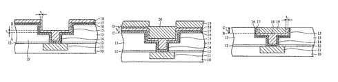
FIG. 1 is a schematic illustration of a substrate having a dielectric layer deposited thereon. In FIG. 1, a substrate 10 is provided that typically includes active and passive devices as well as conductive and dielectric layers that are not shown in order to simplify the drawing. Substrate 10 may include silicon or silicon-germanium, gallium-arsenide, or silicon-on-insulator technology. A conductive layer 11 is formed on substrate 10 by conventional means. Conductive layer 11 may include a metal such as Al, Cu, W, or an Al/Cu alloy. Optionally, conductive layer 11 is deposited on a diffusion barrier layer (not shown) within substrate 10 in order to protect the conductive layer from trace amounts of impurities in substrate 10 that may cause corrosion or oxidation of conductive layer 11. A diffusion barrier layer can also prevent metal ions in conductive layer 11 from diffusing into substrate 10 and diminishing the insulating capability of adjacent dielectric layers. The surface of conductive layer 11 can be planarized to be coplanar with substrate 10.
An etch-stop layer 12 can optionally be deposited on substrate 10. Etch stop layer 12 can be silicon carbide, silicon oxynitride or silicon nitride. The etch-stop layer can be deposited using a conventional chemical vapor deposition (CVD) process or by a plasma enhanced CVD technique. A dielectric layer 13 is then formed on the etch-stop layer 12 by a CVD, plasma enhanced CVD, or by a spin-on method and is comprised of SiO2, phosphosilicate glass (PSG), borophosphosilicate glass (BPSG), or a material with a low dielectric constant (“k”) such as fluorine doped SiO2, carbon doped SiO2, a polysilsesquioxane, a poly(aryl ether), or a fluorinated polyimide. When dielectric layer 13 contains a porous, low k dielectric material, the dielectric layer 13 may be subjected to further processing such as heating or a plasma treatment to increase the density of the layer.
Optionally, a cap layer (not shown) such as silicon oxynitride or silicon nitride can be deposited on dielectric layer 13 to form the top layer in a dielectric stack of layers. In an alternative embodiment, the dielectric stack of layers can be formed by sequentially depositing a first etch stop layer, a first dielectric layer, a second etch stop layer (not shown), a second dielectric layer (not shown) and a cap layer as previously described.
A conventional sequence of steps that includes patterning a photoresist layer (not shown) and using the photoresist as an etch mask while transferring the pattern into the underlying dielectric layer can also be employed to produce a via 14. A similar sequence of steps can be carried out to fabricate a trench 15 overlying via 14. It is also noted that other dual damascene designs are possible in addition to a trench 15 that is centered over a via 14 as in FIG. 1. For example, one trench may be aligned above two or more vias. Furthermore, the trench 15 may not be centered over the via 14 but offset to one side of the via 14 while still uncovering the entire via opening. Note that via 14 extends through etch stop layer 12 to expose underlying conductive layer 11. A standard cleaning process may be performed after the etch steps that form via 14 and trench 15 in order to remove any residue on conductive layer 11 or on etch stop layer 12 and dielectric layer 13.
Referring to FIG. 2, a conformal diffusion barrier layer 16 can be deposited on the sidewalls and bottom of via 14 and trench 15. Diffusion barrier layer 16 can be deposited by a CVD, plasma enhanced CVD, or an atomic layer deposition (ALD) method. The diffusion barrier layer 16 may include Ta, TaN, Ti, TiN, TaSiN, W, or WN or a composite layer of two or more of the aforementioned materials.
A copper seed layer 17 can then be formed on diffusion barrier layer 16 in order to promote the deposition of a thicker first copper layer 18 in a subsequent step. The copper seed layer 17 can be deposited by a physical vapor deposition (PVD) process or by an ionized metal plasma (IMP) sputtering method. The copper seed layer 17 can have a uniform thickness to conform to the shape of diffusion barrier layer 16.
A first copper layer 18 can be deposited by a first electrochemical plating (ECP) process on copper seed layer 17. An exemplary ECP process involves an electroplating composition having current density of about 3–60 A/cm2. The plating bath can include CuSO4, HCl, H2SO4, suppressor(s) and additives. In one embodiment, the ECP solution is maintained at a temperature of about 20–40° C. and a pH in the range of about 1–7. The current density of the ECP solution can be about 3–60 mA/cm2.
The first ECP process may be continued for a duration of time or until via 14 is completely filled with a first copper layer 18 that also forms on the sidewalls and bottom of trench 15 but does not completely fill trench 15. The thickness “t1” of first copper layer 18 (see FIG. 2) within trench 15 can be devised to accommodate a desired outcome. The first copper layer 18 within trench 15 may conform to the shape of the copper seed layer 17. In one embodiment, thickness t1 of first copper layer 18 is equivalent to the distance from the top of seed layer 17 shown as dashed line A to a level indicated by dashed line B. A similar thickness t1 can be formed on the sidewalls of trench 15.
FIG. 5 shows a schematic representation of a conventional electroplating system. Different types conventionally known electroplating cells may be employed for the first ECP process. In one embodiment, DC current 50 is applied to a copper anode 51 in the electroplating solution 52 within the electroplating cell 53 where Cu is converted to Cu2+ ions that migrate to the cathode 54. Put in the context of the embodiment of FIG. 2, cathode 54 may be the copper seed layer 17. The cathode 54 is where Cu2+ ions react with the electrons to form and subsequently deposit Cu. Thus, the following reaction is conducted:
Cu→Cu2++2e (At anode)
Cu2++2e →Cu (At cathode)
Conventional electroplating solutions contain sulfur (S) in the form of sulfates, chlorine (Cl) from hydrochloric acid “HCL” or other chlorine-containing additives and C from carbon-containing additives. Trace amounts of S, Cl, and C are easily trapped within first copper layer 18 and become a source of contamination unless removed.
According to one embodiment of the disclosure, a first annealing step is performed by heating substrate 10 to about 180–200° C. for about 30 seconds to remove S, Cl and C impurities from first copper layer 18. According to one embodiment of the disclosure, the disclosure is that the trench 15 and via 14 are not simultaneously filled in the first ECP process. The incomplete fill of trench 15 enables impurities in via 14 to be more easily removed in the first anneal step. A small grain size of equal or less than about 1 micron can be formed in the first ECP process to improve via fill capability. The first anneal step can increase the copper grain size in first copper layer 18 to equal or less than about 1 microns. The larger grain size after the first anneal step is desirable as it improves the electrical properties of first copper layer 18.
According to another embodiment, a second ECP process is used to deposit a second copper film. FIG. 3 shows the substrate of FIG. 2 having a second copper layer deposited thereon. Referring to FIG. 3, second copper layer 19 is deposited on first copper layer 18, for example using an ECP process or a sputtering technique. The second ECP process can be performed with an electroplating solution that does not contain HCl or a carbon based additive to avoid contaminants in copper layer 19. The duration and the intensity of the second ECP process can be adjusted according to the desired outcome.
The top surface of second copper layer 19 may be uneven having a low section 20 above trench 15 (in a plane indicated by dashed line D.) As used herein, the bottom surface is used to refer to the surface of a layer formed first in a deposition process while a top surface is understood to refer to the surface of a layer that is formed last in a deposition process. A top or bottom surface may be formed in a plane parallel or perpendicular to the substrate 10. Furthermore, a top or bottom surface may be divided into a plurality of sections in which one or more sections are in a plane perpendicular to substrate 10 and one or more sections are in a plane parallel to substrate 10. Thickness “t2” of section 20 in the top surface of second copper layer 19 above the level of dielectric layer 13 is the distance between dashed line D and dashed line C where C is a plane that is coplanar with the top surface of dielectric layer 13. Thickness t2 can be devised to ensure that trench 15 is completely filled by second copper layer 19 above first copper layer 18.
To remove any impurity, a second annealing process may be performed. The device shown in FIG. 3, can be annealed at about 180–200° C. for a duration to remove trace amounts of Cl, C and S impurities as well as any other impurity. The second anneal step may also decrease the copper grain size in second copper layer 19 to about 2 microns. The smaller grain size improves the electrical properties of copper layer 19. The first and second annealing steps can be varied so as to obtain different grain sizes for each of copper layers 18 and 19.
In an alternative embodiment, a copper sputtering process may be used to deposit one or both of the copper layers 18 and 19. Copper sputtering is also known as physical vapor deposition (PVD). A PVD method has the advantage of forming second copper layer 19 without introducing impurities identified above. However, PVD typically has a lower deposition rate than an ECP process.
In an embodiment of the disclosure where PVD technique is employed to deposit copper layer 19, a second anneal step can be performed at a temperature of about 180–200° C. for about 30 seconds to increase copper grain size of copper layer 19 and to form a smooth interface between first and second copper layers 18 and 19, respectively.
Referring to FIG. 4, the dual damascene scheme is completed by a planarization method that may be a chemical-mechanical polishing (CMP) process. The CMP process may involve more than one step. For example, a first CMP step may be used to remove first copper layer 18, second copper layer 19 and copper seed layer 17 above dielectric layer 13. A second CMP step may be employed to remove diffusion barrier layer 16 above dielectric layer 13. A third CMP step called a buffing step may be used to polish dielectric layer 13 and the exposed top surfaces of diffusion barrier 16, copper seed layer 17, first copper layer 18 and second copper layer 19 within trench 15 to form a smoother exposed top surface for each of the aforementioned layers and remove scratches from previous CMP steps. As a result of the CMP process, the exposed top surfaces of diffusion barrier layer 16, copper seed layer 17, first copper layer 18 and second copper layer 19 become coplanar with dielectric layer 13. Note that copper seed layer 17 may be too thin to be distinguishable from first copper layer 18 when the device is cross-sectioned to provide a view as in FIG. 4 during analysis by a scanning electron microscope (SEM) technique. In addition to an exposed top surface, diffusion barrier layer 16 and copper seed layer 17 can have a top surface within via 14 and trench 15 and first copper layer has a top surface within trench 15.
As shown, second copper layer 19 can have a bottom surface comprised of sections that are essentially perpendicular to the surface of substrate 10 and a section that is parallel to the surface of substrate 10. Second copper layer 19 has a thickness t3 of a desired range within trench 15. The thickness t3 represents the distance between the planarized top surface and the section of the bottom surface that is parallel to the surface of substrate 10.
In one embodiment, the disclosure provides a smaller grain size in first copper layer 18 and second copper layer 19 produced as a result of the two step deposition sequence. A small grain size after the second anneal step enables the CMP process to have a wider process window which reduces the cost of the polishing process. In addition, the CMP process is able to produce smoother top surface of first copper layer 18 and of second copper layer 19 by reducing the copper grain size on the exposed sections of the top surface of the aforementioned copper layers to less than 2 microns compared with approximately 2 microns in prior art. Another advantage is that the interconnect comprised of copper seed layer 17, first copper layer 18 and second copper layer 19 has a lower impurity content than copper interconnects fabricated by conventional ECP processes. In addition, the interconnect of the present invention may have a fewer copper defects than an interconnect formed by conventional dual damascene methods.
In another embodiment, the present invention is directed to a copper interconnect structure formed on a semiconductor substrate 10 as depicted in FIG. 4. Substrate 10 has a surface or side on which a semiconductor device will be fabricated. The copper interconnect structure is formed in a via 14 and an overlying trench 15 that are lined with a conformal diffusion barrier layer 16. The via 14 and trench 15 are formed in a stack of dielectric layers that in one embodiment encompasses a dielectric layer 13 formed on an etch stop layer 12. Via 14 and trench 15 each have a bottom, sidewalls and a top. The bottom of via 14 contacts the upper surface of an underlying conductive layer 11 in substrate 10. The bottom surface is the surface of a layer that is formed first in a deposition process and a top surface is the surface of a layer that is formed last in a deposition process, or alternatively, by a CMP process. A top or bottom surface may be formed in a plane that is parallel or perpendicular to the surface of substrate 10. Furthermore, a top or bottom surface may be divided into a plurality of sections in which one or more sections are in a plane that is perpendicular to the surface of substrate 10 and one or more sections are in a plane that is parallel to the surface of substrate 10.
The sidewalls of the via 14 and trench 15 are preferably vertical (i.e., perpendicular to the surface of substrate 10) and are lined with a conformal diffusion barrier layer 16 that also covers the bottom of via 14 and trench 15. The bottom of trench 15 is preferably parallel to the surface of substrate 10 and can be interrupted only by an opening for via 14. Optionally, the via 14 and trench 15 are formed in a stack of dielectric layers comprised of an upper cap layer (not shown) such as silicon carbide, silicon oxynitride, or silicon nitride, a middle dielectric layer 13 and a lower etch stop layer 12. In yet another embodiment (not illustrated) the stack of dielectric layers is formed by sequentially coating a first etch stop layer, a first dielectric layer, a second etch stop layer, a second dielectric layer and a cap layer on substrate 10. In this embodiment, the overlying trench is formed in the cap layer and extends through the second dielectric layer while the via extends from the second etch stop layer through the first dielectric layer and through the first etch stop layer.
Substrate 10 is preferably silicon but may also be based on silicon-germanium, gallium-arsenide, or silicon-on-insulator technology. Conductive layer 11 may include a metal such as Al, Cu, W, or an Al/Cu alloy. In an alternative embodiment, conductive layer 11 is enclosed on the sides and bottom by a diffusion barrier layer (not shown) within substrate 10. Etch stop layer 12 is preferably comprised of silicon nitride, silicon carbide, or silicon oxynitride. Dielectric layer 13 may include SiO2, PSG, BPSG, or a material having a low dielectric constant such as fluorine doped SiO2, carbon doped SiO2, a poly (arylether), a polysilsesquioxane, or a fluorinated polyimide.
The copper interconnect structure may include a conformal copper seed layer 17 formed on the diffusion barrier layer 16, a first copper layer 18 formed on the copper seed layer 17 and which fills the via 14 and partially fills the trench 15 and a second copper layer 19 formed on the first copper layer 18 that fills the trench 15. Thus, the copper interconnect structure has vertical sidewalls, a first planar bottom that coincides with the bottom of the via 14, a second planar bottom that coincides with the bottom of the trench 15, and a planar top that is coplanar with the top surface of the dielectric layer 13. The top of the copper interconnect is comprised of planarized exposed top surfaces of diffusion barrier 16, copper seed layer 17, first copper layer 18, and second copper layer 19. Optionally, when a cap layer is included in the stack of dielectric layers the copper interconnect is coplanar with the top surface of the cap layer.
Diffusion barrier layer 16 is preferably comprised of one or more of Ta, TaN, Ti, TiN, TaSiN, W, or WN. In addition to an exposed top surface, diffusion barrier layer 16 may have a top surface within via 14 and within trench 15. Copper seed layer 17 can have a thickness between about 600–2000 Angstroms and can be formed as a conformal layer on the top surface of diffusion barrier layer 16. In one embodiment, the copper seed layer 17 may be thin enough so that it is not distinguishable from first copper layer 18 when the interconnect is cross-sectioned to provide a cross-sectional view as illustrated in FIG. 4. In addition to an exposed top surface, copper seed layer 17 may have a top surface within via 14 and trench 15.
In one embodiment, the first copper layer 18 may partially fill trench 15 and have a thickness equivalent to the distance between the top surface of copper seed layer 17 (indicated by dashed line A to a level represented by dashed line B.) As shown in FIG. 4, the first copper layer 18 within trench 15 can be formed as a conformal layer on the top surface of the copper seed layer 17. Thus, a similar thickness t1 of first copper layer 18 can be formed on copper seed layer 17 along the sidewalls of trench 15. In addition to an exposed top surface, first copper layer 18 can have a top surface within trench 15.
The top surface of first copper layer 18 within trench 15 forms a smooth interface with the bottom surface of the second copper layer 19. Second copper layer 19 has a planarized and exposed top surface that is coplanar with the top surface of dielectric layer 13 and has a bottom surface comprised of sections that are essentially perpendicular to the surface of substrate 10 and a section that is parallel to the surface of substrate 10. In one embodiment, the grain sizes for first copper layer 18 & the second copper layer 19 can be about 1 micron.
FIG. 6 shows Copper film quality enhancement with two-step deposition according to one embodiment of the disclosure. Referring to FIG. 6A, a defect forming mechanism is numbered consistent with schematic representations of FIGS. 1–4. In FIG. 6A, substrate 10 is shown to have copper interconnect line 11, in electromagnetic communication with via 14 and trench 15. The first copper layer 18 has undergone ECP deposition and annealing as disclosed with respect to FIGS. 1–4. Consequently, defect 25 is sparse and small. On the other hand, trench 15 is deposited with second copper layer 19 and includes larger copper grains 25 and more defects. FIG. 6B shows grain boundary for the various copper layers of FIG. 6A. The figure demonstrate the Cu grain size profile in the metal line after two-step electro-plating.
FIG. 7 comparatively shows enhancement obtained by a two-step deposition according to one embodiment of the disclosure. Referring to embodiment of FIG. 7A, a conventional deposition is performed wherein conductive layer 11 has I10 copper while each of via 14 and trench 15 have deposited therein, respectively, I40 and I60 copper. The embodiment of FIG. 7A was prepared through a single ECP deposition (i.e., only one bath usage). The result was a copper film having high impurity, a poor polish window for CMP and a relatively high cost for the Cu CMP. On the other hand, the Cu film of FIG. 7B was deposited with a two-step deposition in accordance with the embodiments disclosed herein. The copper seed layer 11 was deposited and annealed. Then, via 14 was filled by sputtering (CVD), followed by filling trench 15 through ECP. The results included reduced impurity, excellent polish for Cu CMP and a relatively lower CMP cost.
The principles disclosed herein may be applied with similar benefits for the fabrication of interconnects in logic devices, memory devices, microelectromechanical devices and other related technologies. Moreover, the method of the present invention may be repeated a plurality of times on the same substrate to form a succession of copper interconnect layers that are stacked in various designs.
FIG. 8 shows exemplary grain sizes of copper. In FIG. 8A, circuit 80 is shown to have twelve chips numbered 113. FIG. 8B is an enlarged representations of chip No. 2 of FIG. 8A. FIG. 8C shows chip No. 2 prepared according to conventional methods of Copper deposit and CMP. The smallest grains are about 2 μm and the surface is relatively smooth. In FIG. 8D chip No. 2 is prepared according to the principles disclosed herein. The largest grain size is greater than 5 μm and the surface us rough. In FIG. 8E, copper is deposited in accordance with the principles disclosed herein and the deposition is followed by CMP. The grain size of the largest copper particles of FIG. 8E is less than 2 μm and the surface is smooth. Comparing the grain size shown in FIG. 8E and that of FIG. 8C, it can be readily seen that the embodiments disclosed herein provide substantially smaller grain size and smoothers surface.
While the disclosure has been discussed in reference to embodiments shown herein, it is important to note that the principles of the disclosure are not limited thereto and include permutations and modifications not specifically disclosed.

Claims (28)

1. In a process for forming a copper interconnect in a semiconductor substrate having a via and a trench in a dual damascene structure, the process comprising:
forming a via and a trench on the semiconductor substrate;
using a first electrochemical plating process, depositing a first copper layer in the via;
annealing the first copper layer in the via to remove impurities including carbon;
depositing a second copper layer in the trench, the second copper layer substantially free of HCl/C-based additives; and
annealing the second copper layer to improve grain size and surface roughness.
2. The process of claim 1, wherein the step of depositing a second copper layer further comprises performing an electrochemical plating substantially free from HCl/C to avoid impurities caused by chlorine or carbon.
3. The process of claim 1, wherein the step of depositing a second copper layer further comprises sputtering the second copper layer in the trench.
4. In a process for forming one or more copper (Cu) film on a substrate the Cu film substantially free from defects and impurities, the process comprising:
providing a substrate (10) having formed therein a first conductive layer (11);
depositing an etch stop layer and a dielectric layer over the substrate, the etch-stop layer and the dielectric having a via (14) and a trench (15) positioned to expose the first conductive layer (11);
depositing a diffusion barrier layer (16) and a Cu seed layer (17) to cover at least a portion of the via (14) and the trench (15);
depositing a first Cu layer (17) to at least partially fill the via (14);
annealing the first Cu layer (17) at about 180–200° C. to remove a first impurity;
depositing a second Cu layer (19) to at least partially fill the trench (15); and
annealing the first Cu layer (17) and the second Cu layer (19) at about 180–200° C. to remove a second impurity;
wherein the step of depositing a second Cu layer includes electrochemical plating copper substantially free of HCl and C-based additives to avoid carbon and chlorine impurities.
5. The method of claim 4, wherein the step of depositing a second Cu layer further comprises electrochemical plating copper.
6. The method of claim 4, wherein the step of depositing a second Cu layer further comprises sputtering.
7. The method of claim 4, wherein the step of depositing a second Cu layer further comprises sputtering, the sputtering process substantially free of C, Cl and S impurities.
8. The method of claim 4, wherein the step of annealing the first Cu layer is carried out for about 1–10 minutes.
9. The method of claim 4, wherein the step of annealing the first and the second Cu layer is carried out for about 1–10 minutes.
10. The method of claim 4, wherein the first conductive layer (11) is selected from the group consisting of Al, Cu, W and alloys thereof.
11. A semiconductor device prepared according to the method of claim 4.
12. A process for forming one or more Cu film substantially free from defects and impurities on a substrate, the process comprising:
providing a substrate (10) having formed therein a first conductive layer (11);
depositing an etch stop layer and a dielectric layer over the substrate, the etch-stop layer and the dielectric having a via (14) and a trench (15) positioned to expose the conductive layer (11);
depositing a diffusion barrier layer (16) and a Cu seed layer (17) to cover at least a portion of the via (14) and the trench (15);
depositing a first Cu layer (17) to at least partially fill the via (14);
annealing the first Cu layer (17) at about 180–200° C. to remove a carbon impurity;
depositing a second Cu layer (19) to at least partially fill the trench (15), the second Cu layer deposited through electrochemical plating free of HCL and C-based additive; and
annealing the first Cu layer (17) and the second Cu layer (19) at about 180–200° C. to removed additional impurities.
13. The process of claim 12, further comprising depositing a seed layer.
14. The process of claim 13, wherein the seed layer further comprises copper.
15. The process of claim 12, wherein the conductive layer further comprises aluminum, copper, tungsten or an alloy of aluminum and copper.
16. A process for forming one or more Cu film substantially free from defects and impurities on a substrate, the process comprising:
providing a substrate (10) having formed therein a first conductive layer (11);
depositing an etch stop layer and a dielectric layer over the substrate, the etch-stop layer and the dielectric having a via (14) and a trench (15) positioned to expose the conductive layer (11);
depositing a diffusion barrier layer (16) and a Cu seed layer (17) to cover at least a portion of the via (14) and the trench (15);
depositing a first Cu layer (17) to at least partially fill the via (14);
annealing the first Cu layer (17) at about 180–200° C. to remove a carbon impurity;
depositing a second Cu layer (19) to at least partially fill the trench (15), the second Cu layer deposited through sputtering free of C, Cl and S; and
annealing the first Cu layer (17) and the second Cu layer (19) at about 180–200° C. to removed additional impurities.
17. The process of claim 16, further comprising depositing a seed layer.
18. The process of claim 17, wherein the seed layer further comprises copper.
19. The process of claim 16, wherein the conductive layer further comprises aluminum, copper, tungsten or an alloy of aluminum and copper.
20. A semiconductor device prepared according to the process of claim 16.
21. A method for forming a copper interconnect in a damascene structure comprising:
forming an opening on a substrate;
depositing a first copper layer in the opening using a first plating electrolyte, wherein the electrolyte further comprises chloride ion and carbon-containing additive; and
depositing a second copper layer in the opening using a second plating electrolyte, wherein the second electrolyte is substantially free from chloride ion and carbon-containing additives.
22. The method of claim 21, further comprising annealing the opening after depositing a first copper layer in the opening.
23. The method of claim 21, further comprising annealing the opening after depositing a second copper layer in the opening.
24. The method of claim 21, wherein the step of depositing a second copper layer further comprises sputtering the second copper layer in the opening.
25. A semiconductor device prepared according to the process of claim 21.
26. In a process for forming a copper interconnect in a semiconductor substrate having a via and a trench in a dual damascene structure, the process comprising:
forming a via and a trench on the semiconductor substrate;
using a first electrochemical plating process, depositing a first copper layer in the via,
annealing the via to remove impurities including carbon;
depositing a second copper layer in the trench, the second copper layer substantially free of HCl/C-based additives; and
annealing the via to improve grain size and sufface roughness;
wherein the step of depositing a second copper layer further comprises performing an electrochemical plating substantially free from HCl/C to avoid impurities caused by chlorine or carbon.
27. In a process for forming one or more copper (Cu) film on a substrate the Cu film substantially free from defects and impurities, the process comprising:
providing a substrate (10) having formed therein a first conductive layer (11);
depositing an etch stop layer and a dielectric layer over the substrate, the etch-stop layer and the dielectric having a via (14) and a trench (15) positioned to expose the first conductive layer (11);
depositing a diffusion barrier layer (16) and a Cu seed layer (17) to cover at least a portion of the via (14) and the trench (15);
depositing a first Cu layer (17) to at least partially fill the via (14);
annealing the first Cu layer (17) at about 180–200° C. to remove a first impurity;
depositing a second Cu layer (19) to at least partially fill the trench (15); and
annealing the first Cu layer (17) and the second Cu layer (19) at about 180–200° C. to remove a second impurity;
wherein the step of depositing a second Cu layer further comprises sputtering, the sputtering process substantially free of C, Cl and S impurities.
28. A process for forming one or more Cu film substantially free from defects and impurities on a substrate, the process comprising:
providing a substrate (10) having formed therein a first conductive layer (11);
depositing an etch stop layer and a dielectric layer over the substrate, the etch-stop layer and the dielectric having a via (14) and a trench (15) positioned to expose the conductive layer (11);
depositing a diffusion barrier layer (16) and a Cu seed layer (17) to cover at least a portion of the via (14) and the trench (15);
depositing a first Cu layer (17) to at least partially fill the via (14);
annealing the first Cu layer (17) at about 180–200° C. to remove a carbon impurity;
depositing a second Cu layer (19) to at least partially fill the trench (15), the second Cu layer deposited through sputtering free of C, Cl and 5; and
annealing the first Cu layer (17) and the second Cu layer (19) at about 180–200° C. to removed additional impurities;
wherein the step of depositing a second Cu layer further comprises sputtering, the sputtering process substantially free of C, Cl and S impurities.
US10/987,713 2004-11-12 2004-11-12 Method and apparatus for copper film quality enhancement with two-step deposition Expired - Fee Related US7189650B2 (en)

Priority Applications (3)

Application Number Priority Date Filing Date Title
US10/987,713 US7189650B2 (en) 2004-11-12 2004-11-12 Method and apparatus for copper film quality enhancement with two-step deposition
TW094137274A TWI287246B (en) 2004-11-12 2005-10-25 Method for copper film quality enhancement with two-step deposition
CNB2005101159603A CN100378954C (en) 2004-11-12 2005-11-11 Semiconductor component and method for manufacture copper lead

Applications Claiming Priority (1)

Application Number Priority Date Filing Date Title
US10/987,713 US7189650B2 (en) 2004-11-12 2004-11-12 Method and apparatus for copper film quality enhancement with two-step deposition

Publications (2)

Publication Number Publication Date
US20060105565A1 US20060105565A1 (en) 2006-05-18
US7189650B2 true US7189650B2 (en) 2007-03-13

Family

ID=36386940

Family Applications (1)

Application Number Title Priority Date Filing Date
US10/987,713 Expired - Fee Related US7189650B2 (en) 2004-11-12 2004-11-12 Method and apparatus for copper film quality enhancement with two-step deposition

Country Status (3)

Country Link
US (1) US7189650B2 (en)
CN (1) CN100378954C (en)
TW (1) TWI287246B (en)

Cited By (12)

* Cited by examiner, † Cited by third party
Publication number Priority date Publication date Assignee Title
US20060113669A1 (en) * 2004-11-26 2006-06-01 Nitto Denko Corporation Printed circuit board and manufacturing method thereof
US20080079156A1 (en) * 2006-09-29 2008-04-03 Hynix Semiconductor Inc. Metal line in semiconductor device and method for forming the same
US20080197506A1 (en) * 2007-02-21 2008-08-21 Fujitsu Limited Semiconductor device manufacturing method, semiconductor device, and semiconductor wafer structure
US20090261477A1 (en) * 2006-12-27 2009-10-22 Ji-Ho Hong Semiconductor device and method of manufacturing the same
US20140138239A1 (en) * 2011-04-15 2014-05-22 Novellus Systems, Inc. Method and apparatus for filling interconnect structures
US8890262B2 (en) * 2012-11-29 2014-11-18 Globalfoundries Inc. Semiconductor device having a metal gate recess
US8975531B2 (en) 2013-01-22 2015-03-10 International Business Machines Corporation Composite copper wire interconnect structures and methods of forming
US20150206840A1 (en) * 2014-01-23 2015-07-23 Taiwan Semiconductor Manufacturing Co., Ltd Semiconductor device structure and method of manufacturing the same
US20180151523A1 (en) * 2013-08-29 2018-05-31 Taiwan Semiconductor Manufacturing Company Ltd. Method for manufacturing interconnect structure
WO2018190817A1 (en) * 2017-04-12 2018-10-18 Intel Corporation Integrated circuit interconnects
US10825727B2 (en) 2017-04-28 2020-11-03 Taiwan Semiconductor Manufacturing Company, Ltd. Metal gates of transistors having reduced resistivity
US10985061B2 (en) 2017-04-20 2021-04-20 Taiwan Semiconductor Manufacturing Company, Ltd. Methods for forming contact plugs with reduced corrosion

Families Citing this family (30)

* Cited by examiner, † Cited by third party
Publication number Priority date Publication date Assignee Title
JP2006019708A (en) * 2004-06-04 2006-01-19 Toshiba Corp Method of manufacturing semiconductor device, and the semiconductor device
US7229918B2 (en) * 2005-02-14 2007-06-12 Infineon Technologies Ag Nitrogen rich barrier layers and methods of fabrication thereof
KR100729126B1 (en) * 2005-11-15 2007-06-14 동부일렉트로닉스 주식회사 Metal line formation of semiconductor device and manufacturing method thereof
KR100739975B1 (en) * 2005-12-20 2007-07-16 주식회사 하이닉스반도체 Method of manufacturing a semiconductor device
US7723237B2 (en) * 2006-12-15 2010-05-25 Tokyo Electron Limited Method for selective removal of damaged multi-stack bilayer films
CN101736375B (en) * 2008-11-24 2012-05-23 中芯国际集成电路制造(北京)有限公司 Plating method
CN102044477A (en) * 2009-10-13 2011-05-04 中芯国际集成电路制造(上海)有限公司 Making method of metal plug adapter
CN101694835A (en) * 2009-10-13 2010-04-14 上海宏力半导体制造有限公司 Manufacture method of metal layer
CN102044478B (en) * 2009-10-13 2013-01-30 中芯国际集成电路制造(上海)有限公司 Method for making metal plug
CN102136452B (en) * 2010-01-27 2013-06-12 中芯国际集成电路制造(上海)有限公司 Method for forming copper interconnected structure and CMP (Chemical Mechanical Polishing) equipment for same
JP6039886B2 (en) 2011-04-08 2016-12-07 富士通株式会社 Manufacturing method of semiconductor device
US20140117550A1 (en) * 2012-10-29 2014-05-01 International Business Machines Corporation Semiconductor device including an insulating layer, and method of forming the semiconductor device
US8518825B1 (en) * 2012-12-24 2013-08-27 Shanghai Huali Microelectronics Corporation Method to manufacture trench-first copper interconnection
US9425092B2 (en) * 2013-03-15 2016-08-23 Applied Materials, Inc. Methods for producing interconnects in semiconductor devices
US9349636B2 (en) 2013-09-26 2016-05-24 Intel Corporation Interconnect wires including relatively low resistivity cores
US9496282B2 (en) * 2013-12-02 2016-11-15 International Business Machines Corporation Structure and method to reduce crystal defects in epitaxial fin merge using nitride deposition
US9312273B2 (en) 2013-12-02 2016-04-12 International Business Machines Corporation Structure and method to reduce crystal defects in epitaxial fin merge using nitride deposition
US9496145B2 (en) * 2014-03-19 2016-11-15 Applied Materials, Inc. Electrochemical plating methods
CN103943556A (en) * 2014-04-28 2014-07-23 上海集成电路研发中心有限公司 Method for processing electrocoppering film used for semiconductor copper connection process
CN105084303A (en) * 2014-05-21 2015-11-25 上海蓝沛新材料科技股份有限公司 Micro-nano copper wire and preparation method thereof
US9828687B2 (en) 2014-05-30 2017-11-28 Applied Materials, Inc. Method for electrochemically depositing metal on a reactive metal film
US9840788B2 (en) 2014-05-30 2017-12-12 Applied Materials, Inc. Method for electrochemically depositing metal on a reactive metal film
JP6713809B2 (en) * 2016-03-31 2020-06-24 株式会社荏原製作所 Substrate manufacturing method and substrate
CN108321503B (en) * 2017-01-16 2020-05-15 群创光电股份有限公司 Liquid crystal antenna device
US11121025B2 (en) * 2018-09-27 2021-09-14 Taiwan Semiconductor Manufacturing Company, Ltd. Layer for side wall passivation
CN113363152A (en) * 2020-03-06 2021-09-07 长鑫存储技术有限公司 Semiconductor structure and manufacturing method thereof
CN111293079B (en) * 2020-03-17 2023-06-16 浙江大学 Manufacturing method of ultra-thick adapter plate
CN114477779B (en) * 2021-12-30 2023-09-08 厦门云天半导体科技有限公司 Multi-layer glass substrate process and structure based on heterogeneous bonding
CN117747573A (en) * 2022-09-13 2024-03-22 华为技术有限公司 Chip packaging structure, manufacturing method thereof and electronic equipment
CN116722093B (en) * 2023-08-04 2023-12-08 季华实验室 Display substrate and manufacturing method thereof

Citations (17)

* Cited by examiner, † Cited by third party
Publication number Priority date Publication date Assignee Title
US5948467A (en) 1998-07-24 1999-09-07 Sharp Laboratories Of America, Inc. Enhanced CVD copper adhesion by two-step deposition process
US6022808A (en) * 1998-03-16 2000-02-08 Advanced Micro Devices, Inc. Copper interconnect methodology for enhanced electromigration resistance
US6077780A (en) 1997-12-03 2000-06-20 Advanced Micro Devices, Inc. Method for filling high aspect ratio openings of an integrated circuit to minimize electromigration failure
US6221765B1 (en) 1998-08-31 2001-04-24 Nec Corporation Method for manufacturing a semiconductor device
US6245670B1 (en) 1999-02-19 2001-06-12 Advanced Micro Devices, Inc. Method for filling a dual damascene opening having high aspect ratio to minimize electromigration failure
US6350688B1 (en) * 2000-08-01 2002-02-26 Taiwan Semiconductor Manufacturing Company Via RC improvement for copper damascene and beyond technology
US6350364B1 (en) 2000-02-18 2002-02-26 Taiwan Semiconductor Manufacturing Company Method for improvement of planarity of electroplated copper
US6358840B1 (en) * 2000-09-06 2002-03-19 Advanced Micro Devices, Inc. Forming and filling a recess in interconnect with alloy to minimize electromigration
US6380084B1 (en) * 2000-10-02 2002-04-30 Chartered Semiconductor Manufacturing Inc. Method to form high performance copper damascene interconnects by de-coupling via and metal line filling
US6391777B1 (en) 2001-05-02 2002-05-21 Taiwan Semiconductor Manufacturing Company Two-stage Cu anneal to improve Cu damascene process
US6451682B1 (en) 1998-11-02 2002-09-17 Ulvac, Inc. Method of forming interconnect film
US20020130046A1 (en) * 2001-03-15 2002-09-19 Applied Materials, Inc. Method of forming copper interconnects
US6582569B1 (en) 1999-10-08 2003-06-24 Applied Materials, Inc. Process for sputtering copper in a self ionized plasma
US20030140988A1 (en) 2002-01-28 2003-07-31 Applied Materials, Inc. Electroless deposition method over sub-micron apertures
US20040072423A1 (en) * 2001-01-12 2004-04-15 Jacob Jorne Methods and systems for electro-or electroless-plating of metal in high-aspect ratio features
US20050095847A1 (en) 2002-07-08 2005-05-05 Nec Electronics Corporation Semiconductor device and manufacturing method thereof
US7030016B2 (en) 2004-03-30 2006-04-18 Taiwan Semiconductor Manufacturing Co., Ltd. Post ECP multi-step anneal/H2 treatment to reduce film impurity

Family Cites Families (3)

* Cited by examiner, † Cited by third party
Publication number Priority date Publication date Assignee Title
US6350384B1 (en) * 2000-08-14 2002-02-26 Dow Corning Corporation Silicon containing multi-arm star polymers
US6548395B1 (en) * 2000-11-16 2003-04-15 Advanced Micro Devices, Inc. Method of promoting void free copper interconnects
US6469387B1 (en) * 2000-11-30 2002-10-22 Advanced Micro Devices, Inc. Semiconductor device formed by calcium doping a copper surface using a chemical solution

Patent Citations (17)

* Cited by examiner, † Cited by third party
Publication number Priority date Publication date Assignee Title
US6077780A (en) 1997-12-03 2000-06-20 Advanced Micro Devices, Inc. Method for filling high aspect ratio openings of an integrated circuit to minimize electromigration failure
US6022808A (en) * 1998-03-16 2000-02-08 Advanced Micro Devices, Inc. Copper interconnect methodology for enhanced electromigration resistance
US5948467A (en) 1998-07-24 1999-09-07 Sharp Laboratories Of America, Inc. Enhanced CVD copper adhesion by two-step deposition process
US6221765B1 (en) 1998-08-31 2001-04-24 Nec Corporation Method for manufacturing a semiconductor device
US6451682B1 (en) 1998-11-02 2002-09-17 Ulvac, Inc. Method of forming interconnect film
US6245670B1 (en) 1999-02-19 2001-06-12 Advanced Micro Devices, Inc. Method for filling a dual damascene opening having high aspect ratio to minimize electromigration failure
US6582569B1 (en) 1999-10-08 2003-06-24 Applied Materials, Inc. Process for sputtering copper in a self ionized plasma
US6350364B1 (en) 2000-02-18 2002-02-26 Taiwan Semiconductor Manufacturing Company Method for improvement of planarity of electroplated copper
US6350688B1 (en) * 2000-08-01 2002-02-26 Taiwan Semiconductor Manufacturing Company Via RC improvement for copper damascene and beyond technology
US6358840B1 (en) * 2000-09-06 2002-03-19 Advanced Micro Devices, Inc. Forming and filling a recess in interconnect with alloy to minimize electromigration
US6380084B1 (en) * 2000-10-02 2002-04-30 Chartered Semiconductor Manufacturing Inc. Method to form high performance copper damascene interconnects by de-coupling via and metal line filling
US20040072423A1 (en) * 2001-01-12 2004-04-15 Jacob Jorne Methods and systems for electro-or electroless-plating of metal in high-aspect ratio features
US20020130046A1 (en) * 2001-03-15 2002-09-19 Applied Materials, Inc. Method of forming copper interconnects
US6391777B1 (en) 2001-05-02 2002-05-21 Taiwan Semiconductor Manufacturing Company Two-stage Cu anneal to improve Cu damascene process
US20030140988A1 (en) 2002-01-28 2003-07-31 Applied Materials, Inc. Electroless deposition method over sub-micron apertures
US20050095847A1 (en) 2002-07-08 2005-05-05 Nec Electronics Corporation Semiconductor device and manufacturing method thereof
US7030016B2 (en) 2004-03-30 2006-04-18 Taiwan Semiconductor Manufacturing Co., Ltd. Post ECP multi-step anneal/H2 treatment to reduce film impurity

Non-Patent Citations (1)

* Cited by examiner, † Cited by third party
Title
U.S. Appl. No. 11/347,949, filed Feb. 6, 2006, Feng et al.

Cited By (26)

* Cited by examiner, † Cited by third party
Publication number Priority date Publication date Assignee Title
US20060113669A1 (en) * 2004-11-26 2006-06-01 Nitto Denko Corporation Printed circuit board and manufacturing method thereof
US7521779B2 (en) * 2004-11-26 2009-04-21 Nitto Denko Corporation Roughened printed circuit board
US20090106975A1 (en) * 2004-11-26 2009-04-30 Nitto Denko Corporation Roughened Printed Circuit Board And Manufacturing Method Thereof
US8522427B2 (en) 2004-11-26 2013-09-03 Nitto Denko Corporation Method of manufacturing a printed circuit board
US20080079156A1 (en) * 2006-09-29 2008-04-03 Hynix Semiconductor Inc. Metal line in semiconductor device and method for forming the same
US7648904B2 (en) * 2006-09-29 2010-01-19 Hynix Semiconductor Inc. Metal line in semiconductor device and method for forming the same
US20100117235A1 (en) * 2006-09-29 2010-05-13 Hynix Semiconductor Inc. Metal line in semiconductor device
US8120113B2 (en) 2006-09-29 2012-02-21 Hynix Semiconductor Inc. Metal line in semiconductor device
US20090261477A1 (en) * 2006-12-27 2009-10-22 Ji-Ho Hong Semiconductor device and method of manufacturing the same
US20080197506A1 (en) * 2007-02-21 2008-08-21 Fujitsu Limited Semiconductor device manufacturing method, semiconductor device, and semiconductor wafer structure
US8008189B2 (en) * 2007-02-21 2011-08-30 Fujitsu Semiconductor Limited Semiconductor device manufacturing method, semiconductor device, and semiconductor wafer structure
US10006144B2 (en) * 2011-04-15 2018-06-26 Novellus Systems, Inc. Method and apparatus for filling interconnect structures
US20140138239A1 (en) * 2011-04-15 2014-05-22 Novellus Systems, Inc. Method and apparatus for filling interconnect structures
US8890262B2 (en) * 2012-11-29 2014-11-18 Globalfoundries Inc. Semiconductor device having a metal gate recess
US9466676B2 (en) 2012-11-29 2016-10-11 Globalfoundries Inc. Method for forming a semiconductor device having a metal gate recess
US8975531B2 (en) 2013-01-22 2015-03-10 International Business Machines Corporation Composite copper wire interconnect structures and methods of forming
US11121104B2 (en) * 2013-08-29 2021-09-14 Taiwan Semiconductor Manufacturing Company Ltd. Method for manufacturing interconnect structure
US20180151523A1 (en) * 2013-08-29 2018-05-31 Taiwan Semiconductor Manufacturing Company Ltd. Method for manufacturing interconnect structure
US9184134B2 (en) * 2014-01-23 2015-11-10 Taiwan Semiconductor Manufacturing Co., Ltd. Method of manufacturing a semiconductor device structure
US20150206840A1 (en) * 2014-01-23 2015-07-23 Taiwan Semiconductor Manufacturing Co., Ltd Semiconductor device structure and method of manufacturing the same
WO2018190817A1 (en) * 2017-04-12 2018-10-18 Intel Corporation Integrated circuit interconnects
US11018054B2 (en) 2017-04-12 2021-05-25 Intel Corporation Integrated circuit interconnects
US10985061B2 (en) 2017-04-20 2021-04-20 Taiwan Semiconductor Manufacturing Company, Ltd. Methods for forming contact plugs with reduced corrosion
US10825727B2 (en) 2017-04-28 2020-11-03 Taiwan Semiconductor Manufacturing Company, Ltd. Metal gates of transistors having reduced resistivity
US11430694B2 (en) 2017-04-28 2022-08-30 Taiwan Semiconductor Manufacturing Company, Ltd. Metal gates of transistors having reduced resistivity
US11810819B2 (en) 2017-04-28 2023-11-07 Taiwan Semiconductor Manufacturing Company, Ltd. Metal gates of transistors having reduced resistivity

Also Published As

Publication number Publication date
TW200616017A (en) 2006-05-16
US20060105565A1 (en) 2006-05-18
CN100378954C (en) 2008-04-02
TWI287246B (en) 2007-09-21
CN1790663A (en) 2006-06-21

Similar Documents

Publication Publication Date Title
US7189650B2 (en) Method and apparatus for copper film quality enhancement with two-step deposition
US7030016B2 (en) Post ECP multi-step anneal/H2 treatment to reduce film impurity
US6657304B1 (en) Conformal barrier liner in an integrated circuit interconnect
US7129165B2 (en) Method and structure to improve reliability of copper interconnects
US6566250B1 (en) Method for forming a self aligned capping layer
US7405157B1 (en) Methods for the electrochemical deposition of copper onto a barrier layer of a work piece
US7348672B2 (en) Interconnects with improved reliability
US20080223724A1 (en) Apparatuses for electrochemical deposition, conductive layer, and fabrication methods thereof
JP3116897B2 (en) Fine wiring formation method
US6506668B1 (en) Utilization of annealing enhanced or repaired seed layer to improve copper interconnect reliability
US7374584B2 (en) Interconnects forming method and interconnects forming apparatus
US6340633B1 (en) Method for ramped current density plating of semiconductor vias and trenches
US7253097B2 (en) Integrated circuit system using dual damascene process
US20040121583A1 (en) Method for forming capping barrier layer over copper feature
US20060091551A1 (en) Differentially metal doped copper damascenes
US6482755B1 (en) HDP deposition hillock suppression method in integrated circuits
US6531780B1 (en) Via formation in integrated circuit interconnects
US6368965B1 (en) Method for low stress plating of semiconductor vias and channels
CN101074485B (en) Method of manufacturing electronic component
US20070148967A1 (en) Method for Manufacturing Semiconductor Device
CN116130411A (en) Semiconductor manufacturing method with copper diffusion preventing structure
US11081390B2 (en) Multi-pass plating process with intermediate rinse and dry
US6479898B1 (en) Dielectric treatment in integrated circuit interconnects
US7597787B2 (en) Methods and apparatuses for electrochemical deposition
US20050236181A1 (en) Novel ECP method for preventing the formation of voids and contamination in vias

Legal Events

Date Code Title Description
AS Assignment

Owner name: TAIWAN SEMICONDUCTOR MANUFACTURING CO., LTD., TAIW

Free format text: ASSIGNMENT OF ASSIGNORS INTEREST;ASSIGNORS:LIU, CHI-WEN;FENG, HSIEN-PING;TSAO, JUNG-CHIH;REEL/FRAME:015997/0452

Effective date: 20041101

STCF Information on status: patent grant

Free format text: PATENTED CASE

CC Certificate of correction
FPAY Fee payment

Year of fee payment: 4

FPAY Fee payment

Year of fee payment: 8

FEPP Fee payment procedure

Free format text: MAINTENANCE FEE REMINDER MAILED (ORIGINAL EVENT CODE: REM.); ENTITY STATUS OF PATENT OWNER: LARGE ENTITY

LAPS Lapse for failure to pay maintenance fees

Free format text: PATENT EXPIRED FOR FAILURE TO PAY MAINTENANCE FEES (ORIGINAL EVENT CODE: EXP.); ENTITY STATUS OF PATENT OWNER: LARGE ENTITY

STCH Information on status: patent discontinuation

Free format text: PATENT EXPIRED DUE TO NONPAYMENT OF MAINTENANCE FEES UNDER 37 CFR 1.362

FP Lapsed due to failure to pay maintenance fee

Effective date: 20190313