US7193088B2 - Iridium complexes as light emitting materials and organic light emitting diode device - Google Patents
Iridium complexes as light emitting materials and organic light emitting diode device Download PDFInfo
- Publication number
- US7193088B2 US7193088B2 US10/992,594 US99259404A US7193088B2 US 7193088 B2 US7193088 B2 US 7193088B2 US 99259404 A US99259404 A US 99259404A US 7193088 B2 US7193088 B2 US 7193088B2
- Authority
- US
- United States
- Prior art keywords
- light emitting
- alkyl
- emitting diode
- diode device
- organic light
- Prior art date
- Legal status (The legal status is an assumption and is not a legal conclusion. Google has not performed a legal analysis and makes no representation as to the accuracy of the status listed.)
- Active, expires
Links
- 0 *N1C2=C(C=CC=C2)N2=C1C(=C)C(=C)C2.*N1C2=C(C=CC=C2)N2=C1C(=C)C(=C)[Ir]2.CC.CC.CC.CC Chemical compound *N1C2=C(C=CC=C2)N2=C1C(=C)C(=C)C2.*N1C2=C(C=CC=C2)N2=C1C(=C)C(=C)[Ir]2.CC.CC.CC.CC 0.000 description 6
- AWXGSYPUMWKTBR-UHFFFAOYSA-N C1=CC=C2C(=C1)C1=C(C=CC=C1)N2C1=CC=C(N(C2=CC=C(N3C4=CC=CC=C4C4=C3C=CC=C4)C=C2)C2=CC=C(N3C4=C(C=CC=C4)C4=C3C=CC=C4)C=C2)C=C1 Chemical compound C1=CC=C2C(=C1)C1=C(C=CC=C1)N2C1=CC=C(N(C2=CC=C(N3C4=CC=CC=C4C4=C3C=CC=C4)C=C2)C2=CC=C(N3C4=C(C=CC=C4)C4=C3C=CC=C4)C=C2)C=C1 AWXGSYPUMWKTBR-UHFFFAOYSA-N 0.000 description 3
- JZFQJBXWDZQQQX-UHFFFAOYSA-N C1=CC=C(CN2C3=C(C=CC=C3)N3=C2C2=CC=CC=C2C3)C=C1.CCN1C2=C(C=CC=C2)N2=C1C1=CC=CC=C1C2.COC1=CC=C(CN2C3=C(C=CC=C3)N3=C2C2=CC=C(OC)C=C2C3)C=C1.FC1=CC=C(CN2C3=C(C=CC=C3)N3=C2C2=C(F)C=C(F)C=C2C3)C(F)=C1 Chemical compound C1=CC=C(CN2C3=C(C=CC=C3)N3=C2C2=CC=CC=C2C3)C=C1.CCN1C2=C(C=CC=C2)N2=C1C1=CC=CC=C1C2.COC1=CC=C(CN2C3=C(C=CC=C3)N3=C2C2=CC=C(OC)C=C2C3)C=C1.FC1=CC=C(CN2C3=C(C=CC=C3)N3=C2C2=C(F)C=C(F)C=C2C3)C(F)=C1 JZFQJBXWDZQQQX-UHFFFAOYSA-N 0.000 description 2
- KDOQMLIRFUVJNT-UHFFFAOYSA-N C1=CC=C(N(C2=CC=C(N(C3=CC=C(N(C4=CC=CC=C4)C4=CC5=C(C=CC=C5)C=C4)C=C3)C3=CC=C(N(C4=CC=CC=C4)C4=CC5=C(C=CC=C5)C=C4)C=C3)C=C2)C2=CC=C3C=CC=CC3=C2)C=C1 Chemical compound C1=CC=C(N(C2=CC=C(N(C3=CC=C(N(C4=CC=CC=C4)C4=CC5=C(C=CC=C5)C=C4)C=C3)C3=CC=C(N(C4=CC=CC=C4)C4=CC5=C(C=CC=C5)C=C4)C=C3)C=C2)C2=CC=C3C=CC=CC3=C2)C=C1 KDOQMLIRFUVJNT-UHFFFAOYSA-N 0.000 description 2
- AAAWRMTYUOYENF-UHFFFAOYSA-N CC1=CC2=C(C=C1C)N1=C(C3=CC=CC=C3C1)N2CC1=CC=CC=C1.CC1=CC=C(CN2C3=C(C=CC=C3)N3=C2C2=CC=C(C)C=C2C3)C=C1.FC(F)(F)C1=CC=CC=C1CN1C2=C(C=CC=C2)N2=C1C1=C(C(F)(F)F)C=CC=C1C2 Chemical compound CC1=CC2=C(C=C1C)N1=C(C3=CC=CC=C3C1)N2CC1=CC=CC=C1.CC1=CC=C(CN2C3=C(C=CC=C3)N3=C2C2=CC=C(C)C=C2C3)C=C1.FC(F)(F)C1=CC=CC=C1CN1C2=C(C=CC=C2)N2=C1C1=C(C(F)(F)F)C=CC=C1C2 AAAWRMTYUOYENF-UHFFFAOYSA-N 0.000 description 2
- GEYOCULIXLDCMW-UHFFFAOYSA-N Nc1ccccc1N Chemical compound Nc1ccccc1N GEYOCULIXLDCMW-UHFFFAOYSA-N 0.000 description 2
- LCFXRSKBJWQHON-UHFFFAOYSA-N C(c1ccccc1)[n]1c(-c2ccccc2)nc2ccccc12 Chemical compound C(c1ccccc1)[n]1c(-c2ccccc2)nc2ccccc12 LCFXRSKBJWQHON-UHFFFAOYSA-N 0.000 description 1
- CNZNHEZEMHFMCO-UHFFFAOYSA-K C.C1=CC2=C3C(=C1)O[Al]14(OC5=CC=CC6=C5N1=CC=C6)(OC1=CC=CC5=C1/N4=C\C=C/5)N3=CC=C2 Chemical compound C.C1=CC2=C3C(=C1)O[Al]14(OC5=CC=CC6=C5N1=CC=C6)(OC1=CC=CC5=C1/N4=C\C=C/5)N3=CC=C2 CNZNHEZEMHFMCO-UHFFFAOYSA-K 0.000 description 1
- MFKUBHGRFKSPAC-UHFFFAOYSA-N C.C1=CC=C(N(C2=CC=C(C3=CC=C(N(C4=CC=CC=C4)C4=C5C=CC=CC5=CC=C4)C=C3)C=C2)C2=C3C=CC=CC3=CC=C2)C=C1 Chemical compound C.C1=CC=C(N(C2=CC=C(C3=CC=C(N(C4=CC=CC=C4)C4=C5C=CC=CC5=CC=C4)C=C3)C=C2)C2=C3C=CC=CC3=CC=C2)C=C1 MFKUBHGRFKSPAC-UHFFFAOYSA-N 0.000 description 1
- PLVZVAXONYSQFX-UHFFFAOYSA-N C.C1=CC=C(N2C(C3=CC(C4=NC5=C(C=CC=C5)N4C4=CC=CC=C4)=CC(C4=NC5=C(C=CC=C5)N4C4=CC=CC=C4)=C3)=NC3=C2C=CC=C3)C=C1 Chemical compound C.C1=CC=C(N2C(C3=CC(C4=NC5=C(C=CC=C5)N4C4=CC=CC=C4)=CC(C4=NC5=C(C=CC=C5)N4C4=CC=CC=C4)=C3)=NC3=C2C=CC=C3)C=C1 PLVZVAXONYSQFX-UHFFFAOYSA-N 0.000 description 1
- UGDZSQVVIMJNHG-UHFFFAOYSA-N C.C1=CC=C2C(=C1)C1=C(C=CC=C1)N2C1=CC=C(C2=CC=C(N3C4=C(C=CC=C4)C4=C3C=CC=C4)C=C2)C=C1 Chemical compound C.C1=CC=C2C(=C1)C1=C(C=CC=C1)N2C1=CC=C(C2=CC=C(N3C4=C(C=CC=C4)C4=C3C=CC=C4)C=C2)C=C1 UGDZSQVVIMJNHG-UHFFFAOYSA-N 0.000 description 1
- LJMASXKIUJDDHT-UHFFFAOYSA-N C.C1=CC=C2C(=C1)C1=C(C=CC=C1)N2C1=CC=C(N2C3=C(C=CC=C3)C3=C2C=CC=C3)C=C1 Chemical compound C.C1=CC=C2C(=C1)C1=C(C=CC=C1)N2C1=CC=C(N2C3=C(C=CC=C3)C3=C2C=CC=C3)C=C1 LJMASXKIUJDDHT-UHFFFAOYSA-N 0.000 description 1
- RPMKHARCJXGPPV-UHFFFAOYSA-K C1=CC2=C3C(=C1)O[Al]14(OC5=CC=CC6=C5N1=CC=C6)(OC1=CC=CC5=C1/N4=C\C=C/5)N3=CC=C2.C1=CC=C(C2=CC=NC3=C2C=CC2=C3N=CC=C2C2=CC=CC=C2)C=C1 Chemical compound C1=CC2=C3C(=C1)O[Al]14(OC5=CC=CC6=C5N1=CC=C6)(OC1=CC=CC5=C1/N4=C\C=C/5)N3=CC=C2.C1=CC=C(C2=CC=NC3=C2C=CC2=C3N=CC=C2C2=CC=CC=C2)C=C1 RPMKHARCJXGPPV-UHFFFAOYSA-K 0.000 description 1
- FTYQBMSMSWUNRS-UHFFFAOYSA-N C1=CC=C(C2=NC3=C(C=CC=C3)N2)C=C1.CCI.CCN1C(C2=CC=CC=C2)=NC2=C1C=CC=C2 Chemical compound C1=CC=C(C2=NC3=C(C=CC=C3)N2)C=C1.CCI.CCN1C(C2=CC=CC=C2)=NC2=C1C=CC=C2 FTYQBMSMSWUNRS-UHFFFAOYSA-N 0.000 description 1
- ZMOYYODMASQOEB-UHFFFAOYSA-N C1=CC=C(C2=NC3=C(C=CC=C3)N2)C=C1.CI.CN1C(C2=CC=CC=C2)=NC2=C1C=CC=C2 Chemical compound C1=CC=C(C2=NC3=C(C=CC=C3)N2)C=C1.CI.CN1C(C2=CC=CC=C2)=NC2=C1C=CC=C2 ZMOYYODMASQOEB-UHFFFAOYSA-N 0.000 description 1
- KJNIFUZTVXRVMB-UHFFFAOYSA-N C1=CC=C(C2=NC3=C(C=CC=C3)N2C2=CC=CC=C2)C=C1.NC1=C(NC2=CC=CC=C2)C=CC=C1.O=CC1=CC=CC=C1 Chemical compound C1=CC=C(C2=NC3=C(C=CC=C3)N2C2=CC=CC=C2)C=C1.NC1=C(NC2=CC=CC=C2)C=CC=C1.O=CC1=CC=CC=C1 KJNIFUZTVXRVMB-UHFFFAOYSA-N 0.000 description 1
- LHIZWYJJXVQUEW-UHFFFAOYSA-N C1=CC=C(C2=NN=C(C3=CC=CC=C3)N2C2=C3C=CC=CC3=CC=C2)C=C1.C1=CC=C(C2=NN=C(C3=CC=CC=C3)N2C2=CC=CC=C2)C=C1.C1=CC=C(N2C(C3=CC(C4=NC5=C(C=CC=C5)N4C4=CC=CC=C4)=CC(C4=NC5=C(C=CC=C5)N4C4=CC=CC=C4)=C3)=NC3=C2C=CC=C3)C=C1.CC(C)(C)C1=CC=C(C2=NN=C(C3=CC=C(C4=CC=CC=C4)C=C3)N2C2=CC=CC=C2)C=C1.CC(C)(C)C1=CC=C(C2=NN=C(C3=CC=C(C4=CC=CC=C4)C=C3)O2)C=C1 Chemical compound C1=CC=C(C2=NN=C(C3=CC=CC=C3)N2C2=C3C=CC=CC3=CC=C2)C=C1.C1=CC=C(C2=NN=C(C3=CC=CC=C3)N2C2=CC=CC=C2)C=C1.C1=CC=C(N2C(C3=CC(C4=NC5=C(C=CC=C5)N4C4=CC=CC=C4)=CC(C4=NC5=C(C=CC=C5)N4C4=CC=CC=C4)=C3)=NC3=C2C=CC=C3)C=C1.CC(C)(C)C1=CC=C(C2=NN=C(C3=CC=C(C4=CC=CC=C4)C=C3)N2C2=CC=CC=C2)C=C1.CC(C)(C)C1=CC=C(C2=NN=C(C3=CC=C(C4=CC=CC=C4)C=C3)O2)C=C1 LHIZWYJJXVQUEW-UHFFFAOYSA-N 0.000 description 1
- YUZFSPNRHNHRSE-UHFFFAOYSA-N C1=CC=C(CN2C(C3=CC=CC=C3)=NC3=C2C=CC=C3)C=C1.CCO.NC1=CC=CC=C1N.O=CC1=CC=CC=C1 Chemical compound C1=CC=C(CN2C(C3=CC=CC=C3)=NC3=C2C=CC=C3)C=C1.CCO.NC1=CC=CC=C1N.O=CC1=CC=CC=C1 YUZFSPNRHNHRSE-UHFFFAOYSA-N 0.000 description 1
- APDKBGLXQLAAAO-UHFFFAOYSA-N C1=CC=C(CN2C3=C(C=CC=C3)N3=C2C2=CC=CC=C2C3)C=C1.C1=CC=C(N2C3=C(C=CC=C3)N3=C2C2=CC=CC=C2C3)C=C1.CCN1C2=C(C=CC=C2)N2=C1C1=CC=CC=C1C2.CN1C2=C(C=CC=C2)N2=C1C1=CC=CC=C1C2 Chemical compound C1=CC=C(CN2C3=C(C=CC=C3)N3=C2C2=CC=CC=C2C3)C=C1.C1=CC=C(N2C3=C(C=CC=C3)N3=C2C2=CC=CC=C2C3)C=C1.CCN1C2=C(C=CC=C2)N2=C1C1=CC=CC=C1C2.CN1C2=C(C=CC=C2)N2=C1C1=CC=CC=C1C2 APDKBGLXQLAAAO-UHFFFAOYSA-N 0.000 description 1
- GMOGQBYIYONDSG-UHFFFAOYSA-N C1=CC=C(N(C2=CC=C(C3=CC=C(N(C4=CC=CC=C4)C4=C5C=CC=CC5=C5/C=C\C=C/C5=C4)C=C3)C=C2)C2=C3C=CC=CC3=C3C=CC=CC3=C2)C=C1.C1=CC=C(N(C2=CC=C(C3=CC=C(N(C4=CC=CC=C4)C4=C5C=CC=CC5=CC=C4)C=C3)C=C2)C2=C3C=CC=CC3=CC=C2)C=C1.C1=CC=C(N(C2=CC=C(C3=CC=C(N4C5=CC=CC=C5C5=C4C=CC=C5)C=C3)C=C2)C2=C3C=CC=CC3=CC=C2)C=C1.CC1=CC=CC(N(C2=CC=CC=C2)C2=CC=C(C3=CC=C(N(C4=CC=CC=C4)C4=CC(C)=CC=C4)C=C3)C=C2)=C1 Chemical compound C1=CC=C(N(C2=CC=C(C3=CC=C(N(C4=CC=CC=C4)C4=C5C=CC=CC5=C5/C=C\C=C/C5=C4)C=C3)C=C2)C2=C3C=CC=CC3=C3C=CC=CC3=C2)C=C1.C1=CC=C(N(C2=CC=C(C3=CC=C(N(C4=CC=CC=C4)C4=C5C=CC=CC5=CC=C4)C=C3)C=C2)C2=C3C=CC=CC3=CC=C2)C=C1.C1=CC=C(N(C2=CC=C(C3=CC=C(N4C5=CC=CC=C5C5=C4C=CC=C5)C=C3)C=C2)C2=C3C=CC=CC3=CC=C2)C=C1.CC1=CC=CC(N(C2=CC=CC=C2)C2=CC=C(C3=CC=C(N(C4=CC=CC=C4)C4=CC(C)=CC=C4)C=C3)C=C2)=C1 GMOGQBYIYONDSG-UHFFFAOYSA-N 0.000 description 1
- OISUMYVIIZHNQH-UHFFFAOYSA-N C1=CC=C(N(C2=CC=C(N(C3=CC=C(N(C4=CC=CC=C4)C4=CC5=C(C=CC=C5)C=C4)C=C3)C3=CC=C(N(C4=CC=CC=C4)C4=CC5=C(C=C4)/C=C\C=C/5)C=C3)C=C2)C2=CC=C3C=CC=CC3=C2)C=C1.C1=CC=C2C(=C1)C1=N3/C2=N\C2=C4C=CC=CC4=C4/N=C5/C6=CC=CC=C6C6=N5[Cu@@]3(N24)N2C(=N1)C1C=CC=CC1/C2=N/6.CC1=CC=CC(N(C2=CC=CC=C2)C2=CC=C(N(C3=CC=C(N(C4=CC=CC=C4)C4=CC(C)=CC=C4)C=C3)C3=CC=C(N(C4=CC=CC=C4)C4=CC(C)=CC=C4)C=C3)C=C2)=C1 Chemical compound C1=CC=C(N(C2=CC=C(N(C3=CC=C(N(C4=CC=CC=C4)C4=CC5=C(C=CC=C5)C=C4)C=C3)C3=CC=C(N(C4=CC=CC=C4)C4=CC5=C(C=C4)/C=C\C=C/5)C=C3)C=C2)C2=CC=C3C=CC=CC3=C2)C=C1.C1=CC=C2C(=C1)C1=N3/C2=N\C2=C4C=CC=CC4=C4/N=C5/C6=CC=CC=C6C6=N5[Cu@@]3(N24)N2C(=N1)C1C=CC=CC1/C2=N/6.CC1=CC=CC(N(C2=CC=CC=C2)C2=CC=C(N(C3=CC=C(N(C4=CC=CC=C4)C4=CC(C)=CC=C4)C=C3)C3=CC=C(N(C4=CC=CC=C4)C4=CC(C)=CC=C4)C=C3)C=C2)=C1 OISUMYVIIZHNQH-UHFFFAOYSA-N 0.000 description 1
- GEQBRULPNIVQPP-UHFFFAOYSA-N C1=CC=C(N2C(C3=CC(C4=NC5=C(C=CC=C5)N4C4=CC=CC=C4)=CC(C4=NC5=C(C=CC=C5)N4C4=CC=CC=C4)=C3)=NC3=C2C=CC=C3)C=C1 Chemical compound C1=CC=C(N2C(C3=CC(C4=NC5=C(C=CC=C5)N4C4=CC=CC=C4)=CC(C4=NC5=C(C=CC=C5)N4C4=CC=CC=C4)=C3)=NC3=C2C=CC=C3)C=C1 GEQBRULPNIVQPP-UHFFFAOYSA-N 0.000 description 1
- DVNOWTJCOPZGQA-UHFFFAOYSA-N C1=CC=C2C(=C1)C1=C(C=CC=C1)N2C1=CC(N2C3=CC=CC=C3C3=C2C=CC=C3)=CC(N2C3=CC=CC=C3C3=C2/C=C\C=C/3)=C1 Chemical compound C1=CC=C2C(=C1)C1=C(C=CC=C1)N2C1=CC(N2C3=CC=CC=C3C3=C2C=CC=C3)=CC(N2C3=CC=CC=C3C3=C2/C=C\C=C/3)=C1 DVNOWTJCOPZGQA-UHFFFAOYSA-N 0.000 description 1
- PEFQUVAWPXADGI-UHFFFAOYSA-N C1=CC=C2C(=C1)C1=C(C=CC=C1)N2C1=CC(N2C3=CC=CC=C3C3=C2C=CC=C3)=CC(N2C3=CC=CC=C3C3=C2C=CC=C3)=C1.C1=CC=C2C(=C1)C1=C(C=CC=C1)N2C1=CC=C(C2=CC(C3=CC=C(N4C5=CC=CC=C5C5=C4C=CC=C5)C=C3)=CC(C3=CC=C(N4C5=CC=CC=C5C5=C4C=CC=C5)C=C3)=C2)C=C1.C1=CC=C2C(=C1)C1=C(C=CC=C1)N2C1=CC=C(C2=CC=C(N3C4=C(C=CC=C4)C4=C3C=CC=C4)C=C2)C=C1.C1=CC=C2C(=C1)C1=C(C=CC=C1)N2C1=CC=CC(N2C3=CC=CC=C3C3=C2C=CC=C3)=C1 Chemical compound C1=CC=C2C(=C1)C1=C(C=CC=C1)N2C1=CC(N2C3=CC=CC=C3C3=C2C=CC=C3)=CC(N2C3=CC=CC=C3C3=C2C=CC=C3)=C1.C1=CC=C2C(=C1)C1=C(C=CC=C1)N2C1=CC=C(C2=CC(C3=CC=C(N4C5=CC=CC=C5C5=C4C=CC=C5)C=C3)=CC(C3=CC=C(N4C5=CC=CC=C5C5=C4C=CC=C5)C=C3)=C2)C=C1.C1=CC=C2C(=C1)C1=C(C=CC=C1)N2C1=CC=C(C2=CC=C(N3C4=C(C=CC=C4)C4=C3C=CC=C4)C=C2)C=C1.C1=CC=C2C(=C1)C1=C(C=CC=C1)N2C1=CC=CC(N2C3=CC=CC=C3C3=C2C=CC=C3)=C1 PEFQUVAWPXADGI-UHFFFAOYSA-N 0.000 description 1
- KZHMVZCFWLFIIO-UHFFFAOYSA-N C1=CC=C2C(=C1)C1=C(C=CC=C1)N2C1=CC=C(N(C2=CC=C(N3C4=CC=CC=C4C4=C3C=CC=C4)C=C2)C2=CC=C(N3C4=C(C=CC=C4)C4=C3C=CC=C4)C=C2)C=C1.CC1=CC=CC(N(C2=CC=CC(C)=C2)C2=CC=C(C3=CC=C(N(C4=CC=CC(C)=C4)C4=CC(C)=CC=C4)C(C)=C3)C=C2C)=C1.CCN(CC)C1=CC=C(C(C2=CC=C(C)C=C2)C2=C(C)C=C(N(CC)CC)C=C2)C(C)=C1 Chemical compound C1=CC=C2C(=C1)C1=C(C=CC=C1)N2C1=CC=C(N(C2=CC=C(N3C4=CC=CC=C4C4=C3C=CC=C4)C=C2)C2=CC=C(N3C4=C(C=CC=C4)C4=C3C=CC=C4)C=C2)C=C1.CC1=CC=CC(N(C2=CC=CC(C)=C2)C2=CC=C(C3=CC=C(N(C4=CC=CC(C)=C4)C4=CC(C)=CC=C4)C(C)=C3)C=C2C)=C1.CCN(CC)C1=CC=C(C(C2=CC=C(C)C=C2)C2=C(C)C=C(N(CC)CC)C=C2)C(C)=C1 KZHMVZCFWLFIIO-UHFFFAOYSA-N 0.000 description 1
- VUBWEGBUHKIPSB-UHFFFAOYSA-N C1=CC=C2C(=C1)C1=C(C=CC=C1)N2C1=CC=C(N2C3=C(C=CC=C3)C3=C2C=CC=C3)C=C1.CC1=CC(N2C3=C(C=CC=C3)C3=C2C=CC=C3)=CC=C1C1=C(C)C=C(N2C3=CC=CC=C3C3=C2C=CC=C3)C=C1 Chemical compound C1=CC=C2C(=C1)C1=C(C=CC=C1)N2C1=CC=C(N2C3=C(C=CC=C3)C3=C2C=CC=C3)C=C1.CC1=CC(N2C3=C(C=CC=C3)C3=C2C=CC=C3)=CC=C1C1=C(C)C=C(N2C3=CC=CC=C3C3=C2C=CC=C3)C=C1 VUBWEGBUHKIPSB-UHFFFAOYSA-N 0.000 description 1
- SEKZYDPIURDWCT-UHFFFAOYSA-N C1=CC=C2C(=C1)C1=NC3=C4C=CC=CC4=C4/N=C5/C6=CC=CC=C6C6=N5[Cu@@]5(N34)N3/C(=N\C2=N15)C1C=CC=CC1/C3=N/6 Chemical compound C1=CC=C2C(=C1)C1=NC3=C4C=CC=CC4=C4/N=C5/C6=CC=CC=C6C6=N5[Cu@@]5(N34)N3/C(=N\C2=N15)C1C=CC=CC1/C3=N/6 SEKZYDPIURDWCT-UHFFFAOYSA-N 0.000 description 1
- FEGRJKSRSXQQEA-UHFFFAOYSA-N C1=CC=C2C(=C1)CN1=C2NC2=C1C=CC=C2.FC(F)(F)C1=CC=C2C(=C1)CN1=C2N(C2=CC=CC=C2)C2=C1C=CC=C2.FC1=CC(F)=C2C(=C1)CN1=C2N(C2=CC=CC=C2)C2=C1C=CC=C2.FC1=CC=C2C(=C1)CN1=C2N(C2=CC=CC=C2)C2=C1C=CC=C2 Chemical compound C1=CC=C2C(=C1)CN1=C2NC2=C1C=CC=C2.FC(F)(F)C1=CC=C2C(=C1)CN1=C2N(C2=CC=CC=C2)C2=C1C=CC=C2.FC1=CC(F)=C2C(=C1)CN1=C2N(C2=CC=CC=C2)C2=C1C=CC=C2.FC1=CC=C2C(=C1)CN1=C2N(C2=CC=CC=C2)C2=C1C=CC=C2 FEGRJKSRSXQQEA-UHFFFAOYSA-N 0.000 description 1
- UOKGEUYIJLWCPZ-UHFFFAOYSA-N CC1=CC(N)=C(N)C=C1C.CC1=CC2=C(C=C1C)N(CC1=CC=CC=C1)C(C1=CC=CC=C1)=N2.CCO.O=CC1=CC=CC=C1 Chemical compound CC1=CC(N)=C(N)C=C1C.CC1=CC2=C(C=C1C)N(CC1=CC=CC=C1)C(C1=CC=CC=C1)=N2.CCO.O=CC1=CC=CC=C1 UOKGEUYIJLWCPZ-UHFFFAOYSA-N 0.000 description 1
- OTHPXLKWBBVJMY-UHFFFAOYSA-N CC1=CC2=C(C=C1C)N1=C(C3=CC=CC=C3C1)N2CC1=CC=CC=C1 Chemical compound CC1=CC2=C(C=C1C)N1=C(C3=CC=CC=C3C1)N2CC1=CC=CC=C1 OTHPXLKWBBVJMY-UHFFFAOYSA-N 0.000 description 1
- DUENOQCDRJCDCL-UHFFFAOYSA-N CC1=CC=C(C=O)C=C1.CC1=CC=C(CN2C(C3=CC=C(C)C=C3)=NC3=C2C=CC=C3)C=C1.CCO.NC1=CC=CC=C1N Chemical compound CC1=CC=C(C=O)C=C1.CC1=CC=C(CN2C(C3=CC=C(C)C=C3)=NC3=C2C=CC=C3)C=C1.CCO.NC1=CC=CC=C1N DUENOQCDRJCDCL-UHFFFAOYSA-N 0.000 description 1
- FWVHYYVOGXKISO-UHFFFAOYSA-N CC1=CC=C(CN2C3=C(C=CC=C3)N3=C2C2=CC=C(C)C=C2C3)C=C1.COC1=CC=C(CN2C3=C(C=CC=C3)N3=C2C2=CC=C(C)C=C2C3)C=C1.FC(F)(F)C1=CC=CC=C1CN1C2=C(C=CC=C2)N2=C1C1=C(C(F)(F)F)C=CC=C1C2.FC1=CC=C(CN2C3=C(C=CC=C3)N3=C2C2=C(F)C=C(F)C=C2C3)C(F)=C1 Chemical compound CC1=CC=C(CN2C3=C(C=CC=C3)N3=C2C2=CC=C(C)C=C2C3)C=C1.COC1=CC=C(CN2C3=C(C=CC=C3)N3=C2C2=CC=C(C)C=C2C3)C=C1.FC(F)(F)C1=CC=CC=C1CN1C2=C(C=CC=C2)N2=C1C1=C(C(F)(F)F)C=CC=C1C2.FC1=CC=C(CN2C3=C(C=CC=C3)N3=C2C2=C(F)C=C(F)C=C2C3)C(F)=C1 FWVHYYVOGXKISO-UHFFFAOYSA-N 0.000 description 1
- UFVXQDWNSAGPHN-UHFFFAOYSA-K CC1=N2C3=C(C=CC=C3O[AlH]23(OC2=CC=C(C4=CC=CC=C4)C=C2)OC2=CC=CC4=C2N3=C(C)C=C4)C=C1 Chemical compound CC1=N2C3=C(C=CC=C3O[AlH]23(OC2=CC=C(C4=CC=CC=C4)C=C2)OC2=CC=CC4=C2N3=C(C)C=C4)C=C1 UFVXQDWNSAGPHN-UHFFFAOYSA-K 0.000 description 1
- VCZYLIUDXOJZLL-UHFFFAOYSA-F CC1=N2C3=C(C=CC=C3O[AlH]23(OC2=CC=C(C4=CC=CC=C4)C=C2)OC2=CC=CC4=C2N3=C(C)C=C4)C=C1.CC1=N2C3=C(C=CC=C3O[AlH]23(OC2=CC=CC=C2)OC2=CC=CC4=C2N3=C(C)C=C4)C=C1.CC1=N2C3=C(C=CC=C3O[AlH]23(O[Si](C2=CC=CC=C2)(C2=CC=CC=C2)C2=CC=CC=C2)OC2=CC=CC4=C2N3=C(C)C=C4)C=C1.CC1=NC2=C(C=CC3=C2N=C(C)C=C3C2=CC=CC=C2)C(C2=CC=CC=C2)=C1 Chemical compound CC1=N2C3=C(C=CC=C3O[AlH]23(OC2=CC=C(C4=CC=CC=C4)C=C2)OC2=CC=CC4=C2N3=C(C)C=C4)C=C1.CC1=N2C3=C(C=CC=C3O[AlH]23(OC2=CC=CC=C2)OC2=CC=CC4=C2N3=C(C)C=C4)C=C1.CC1=N2C3=C(C=CC=C3O[AlH]23(O[Si](C2=CC=CC=C2)(C2=CC=CC=C2)C2=CC=CC=C2)OC2=CC=CC4=C2N3=C(C)C=C4)C=C1.CC1=NC2=C(C=CC3=C2N=C(C)C=C3C2=CC=CC=C2)C(C2=CC=CC=C2)=C1 VCZYLIUDXOJZLL-UHFFFAOYSA-F 0.000 description 1
- STTGYIUESPWXOW-UHFFFAOYSA-N CC1=NC2=C(C=CC3=C2N=C(C)C=C3C2=CC=CC=C2)C(C2=CC=CC=C2)=C1 Chemical compound CC1=NC2=C(C=CC3=C2N=C(C)C=C3C2=CC=CC=C2)C(C2=CC=CC=C2)=C1 STTGYIUESPWXOW-UHFFFAOYSA-N 0.000 description 1
- IRNMAOABXDRHRL-UHFFFAOYSA-N CCO.COC1=CC=C(C=O)C=C1.COC1=CC=C(CN2C(C3=CC=C(OC)C=C3)=NC3=C2C=CC=C3)C=C1.NC1=CC=CC=C1N Chemical compound CCO.COC1=CC=C(C=O)C=C1.COC1=CC=C(CN2C(C3=CC=C(OC)C=C3)=NC3=C2C=CC=C3)C=C1.NC1=CC=CC=C1N IRNMAOABXDRHRL-UHFFFAOYSA-N 0.000 description 1
- HKJLCTRXYFYESZ-UHFFFAOYSA-N CCO.FC(F)(F)C1=CC=CC=C1CN1C(C2=CC=CC=C2C(F)(F)F)=NC2=C1C=CC=C2.NC1=CC=CC=C1N.O=CC1=CC=CC=C1C(F)(F)F Chemical compound CCO.FC(F)(F)C1=CC=CC=C1CN1C(C2=CC=CC=C2C(F)(F)F)=NC2=C1C=CC=C2.NC1=CC=CC=C1N.O=CC1=CC=CC=C1C(F)(F)F HKJLCTRXYFYESZ-UHFFFAOYSA-N 0.000 description 1
- WTZGMZSDHTUBED-UHFFFAOYSA-N CCO.FC1=CC=C(CN2C(C3=C(F)C=C(F)C=C3)=NC3=C2C=CC=C3)C(F)=C1.NC1=CC=CC=C1N.O=CC1=CC=C(F)C=C1F Chemical compound CCO.FC1=CC=C(CN2C(C3=C(F)C=C(F)C=C3)=NC3=C2C=CC=C3)C(F)=C1.NC1=CC=CC=C1N.O=CC1=CC=C(F)C=C1F WTZGMZSDHTUBED-UHFFFAOYSA-N 0.000 description 1
- QZHSOBQECJGFKW-UHFFFAOYSA-N FC(F)(F)C1=CC=C(C2=NC3=C(C=CC=C3)N2C2=CC=CC=C2)C=C1.NC1=CC=CC=C1NC1=CC=CC=C1.[H]C(=O)C1=CC=C(C(F)(F)F)C=C1 Chemical compound FC(F)(F)C1=CC=C(C2=NC3=C(C=CC=C3)N2C2=CC=CC=C2)C=C1.NC1=CC=CC=C1NC1=CC=CC=C1.[H]C(=O)C1=CC=C(C(F)(F)F)C=C1 QZHSOBQECJGFKW-UHFFFAOYSA-N 0.000 description 1
- LTKIOPQDTPRNLA-UHFFFAOYSA-N FC1=CC=C(C2=NC3=C(C=CC=C3)N2C2=CC=CC=C2)C(F)=C1.NC1=CC=CC=C1NC1=CC=CC=C1.[H]C(=O)C1=C(F)C=C(F)C=C1 Chemical compound FC1=CC=C(C2=NC3=C(C=CC=C3)N2C2=CC=CC=C2)C(F)=C1.NC1=CC=CC=C1NC1=CC=CC=C1.[H]C(=O)C1=C(F)C=C(F)C=C1 LTKIOPQDTPRNLA-UHFFFAOYSA-N 0.000 description 1
- RKJJHNSTVYSTCH-UHFFFAOYSA-N FC1=CC=C(C2=NC3=C(C=CC=C3)N2C2=CC=CC=C2)C=C1.NC1=CC=CC=C1NC1=CC=CC=C1.[H]C(=O)C1=CC=C(F)C=C1 Chemical compound FC1=CC=C(C2=NC3=C(C=CC=C3)N2C2=CC=CC=C2)C=C1.NC1=CC=CC=C1NC1=CC=CC=C1.[H]C(=O)C1=CC=C(F)C=C1 RKJJHNSTVYSTCH-UHFFFAOYSA-N 0.000 description 1
- FUDCGUXFJVMOGC-UHFFFAOYSA-N Fc1cc(F)c(C[n]2c(-c(ccc(F)c3)c3F)nc3ccccc23)cc1 Chemical compound Fc1cc(F)c(C[n]2c(-c(ccc(F)c3)c3F)nc3ccccc23)cc1 FUDCGUXFJVMOGC-UHFFFAOYSA-N 0.000 description 1
- WCGPCBACLBHDCI-UHFFFAOYSA-N O=Cc(ccc(F)c1)c1F Chemical compound O=Cc(ccc(F)c1)c1F WCGPCBACLBHDCI-UHFFFAOYSA-N 0.000 description 1
- HUMNYLRZRPPJDN-UHFFFAOYSA-N O=Cc1ccccc1 Chemical compound O=Cc1ccccc1 HUMNYLRZRPPJDN-UHFFFAOYSA-N 0.000 description 1
Images


Classifications
-
- C—CHEMISTRY; METALLURGY
- C07—ORGANIC CHEMISTRY
- C07F—ACYCLIC, CARBOCYCLIC OR HETEROCYCLIC COMPOUNDS CONTAINING ELEMENTS OTHER THAN CARBON, HYDROGEN, HALOGEN, OXYGEN, NITROGEN, SULFUR, SELENIUM OR TELLURIUM
- C07F15/00—Compounds containing elements of Groups 8, 9, 10 or 18 of the Periodic System
- C07F15/0006—Compounds containing elements of Groups 8, 9, 10 or 18 of the Periodic System compounds of the platinum group
- C07F15/0033—Iridium compounds
-
- C—CHEMISTRY; METALLURGY
- C09—DYES; PAINTS; POLISHES; NATURAL RESINS; ADHESIVES; COMPOSITIONS NOT OTHERWISE PROVIDED FOR; APPLICATIONS OF MATERIALS NOT OTHERWISE PROVIDED FOR
- C09K—MATERIALS FOR MISCELLANEOUS APPLICATIONS, NOT PROVIDED FOR ELSEWHERE
- C09K11/00—Luminescent, e.g. electroluminescent, chemiluminescent materials
- C09K11/06—Luminescent, e.g. electroluminescent, chemiluminescent materials containing organic luminescent materials
-
- H—ELECTRICITY
- H05—ELECTRIC TECHNIQUES NOT OTHERWISE PROVIDED FOR
- H05B—ELECTRIC HEATING; ELECTRIC LIGHT SOURCES NOT OTHERWISE PROVIDED FOR; CIRCUIT ARRANGEMENTS FOR ELECTRIC LIGHT SOURCES, IN GENERAL
- H05B33/00—Electroluminescent light sources
- H05B33/12—Light sources with substantially two-dimensional radiating surfaces
- H05B33/14—Light sources with substantially two-dimensional radiating surfaces characterised by the chemical or physical composition or the arrangement of the electroluminescent material, or by the simultaneous addition of the electroluminescent material in or onto the light source
-
- H—ELECTRICITY
- H10—SEMICONDUCTOR DEVICES; ELECTRIC SOLID-STATE DEVICES NOT OTHERWISE PROVIDED FOR
- H10K—ORGANIC ELECTRIC SOLID-STATE DEVICES
- H10K85/00—Organic materials used in the body or electrodes of devices covered by this subclass
- H10K85/30—Coordination compounds
- H10K85/341—Transition metal complexes, e.g. Ru(II)polypyridine complexes
- H10K85/342—Transition metal complexes, e.g. Ru(II)polypyridine complexes comprising iridium
-
- C—CHEMISTRY; METALLURGY
- C09—DYES; PAINTS; POLISHES; NATURAL RESINS; ADHESIVES; COMPOSITIONS NOT OTHERWISE PROVIDED FOR; APPLICATIONS OF MATERIALS NOT OTHERWISE PROVIDED FOR
- C09K—MATERIALS FOR MISCELLANEOUS APPLICATIONS, NOT PROVIDED FOR ELSEWHERE
- C09K2211/00—Chemical nature of organic luminescent or tenebrescent compounds
- C09K2211/10—Non-macromolecular compounds
- C09K2211/1018—Heterocyclic compounds
- C09K2211/1025—Heterocyclic compounds characterised by ligands
- C09K2211/1044—Heterocyclic compounds characterised by ligands containing two nitrogen atoms as heteroatoms
-
- C—CHEMISTRY; METALLURGY
- C09—DYES; PAINTS; POLISHES; NATURAL RESINS; ADHESIVES; COMPOSITIONS NOT OTHERWISE PROVIDED FOR; APPLICATIONS OF MATERIALS NOT OTHERWISE PROVIDED FOR
- C09K—MATERIALS FOR MISCELLANEOUS APPLICATIONS, NOT PROVIDED FOR ELSEWHERE
- C09K2211/00—Chemical nature of organic luminescent or tenebrescent compounds
- C09K2211/18—Metal complexes
- C09K2211/185—Metal complexes of the platinum group, i.e. Os, Ir, Pt, Ru, Rh or Pd
-
- H—ELECTRICITY
- H10—SEMICONDUCTOR DEVICES; ELECTRIC SOLID-STATE DEVICES NOT OTHERWISE PROVIDED FOR
- H10K—ORGANIC ELECTRIC SOLID-STATE DEVICES
- H10K2101/00—Properties of the organic materials covered by group H10K85/00
- H10K2101/10—Triplet emission
-
- H—ELECTRICITY
- H10—SEMICONDUCTOR DEVICES; ELECTRIC SOLID-STATE DEVICES NOT OTHERWISE PROVIDED FOR
- H10K—ORGANIC ELECTRIC SOLID-STATE DEVICES
- H10K50/00—Organic light-emitting devices
- H10K50/10—OLEDs or polymer light-emitting diodes [PLED]
- H10K50/11—OLEDs or polymer light-emitting diodes [PLED] characterised by the electroluminescent [EL] layers
-
- H—ELECTRICITY
- H10—SEMICONDUCTOR DEVICES; ELECTRIC SOLID-STATE DEVICES NOT OTHERWISE PROVIDED FOR
- H10K—ORGANIC ELECTRIC SOLID-STATE DEVICES
- H10K85/00—Organic materials used in the body or electrodes of devices covered by this subclass
- H10K85/30—Coordination compounds
- H10K85/311—Phthalocyanine
-
- H—ELECTRICITY
- H10—SEMICONDUCTOR DEVICES; ELECTRIC SOLID-STATE DEVICES NOT OTHERWISE PROVIDED FOR
- H10K—ORGANIC ELECTRIC SOLID-STATE DEVICES
- H10K85/00—Organic materials used in the body or electrodes of devices covered by this subclass
- H10K85/30—Coordination compounds
- H10K85/321—Metal complexes comprising a group IIIA element, e.g. Tris (8-hydroxyquinoline) gallium [Gaq3]
- H10K85/324—Metal complexes comprising a group IIIA element, e.g. Tris (8-hydroxyquinoline) gallium [Gaq3] comprising aluminium, e.g. Alq3
-
- H—ELECTRICITY
- H10—SEMICONDUCTOR DEVICES; ELECTRIC SOLID-STATE DEVICES NOT OTHERWISE PROVIDED FOR
- H10K—ORGANIC ELECTRIC SOLID-STATE DEVICES
- H10K85/00—Organic materials used in the body or electrodes of devices covered by this subclass
- H10K85/60—Organic compounds having low molecular weight
- H10K85/615—Polycyclic condensed aromatic hydrocarbons, e.g. anthracene
-
- H—ELECTRICITY
- H10—SEMICONDUCTOR DEVICES; ELECTRIC SOLID-STATE DEVICES NOT OTHERWISE PROVIDED FOR
- H10K—ORGANIC ELECTRIC SOLID-STATE DEVICES
- H10K85/00—Organic materials used in the body or electrodes of devices covered by this subclass
- H10K85/60—Organic compounds having low molecular weight
- H10K85/631—Amine compounds having at least two aryl rest on at least one amine-nitrogen atom, e.g. triphenylamine
-
- H—ELECTRICITY
- H10—SEMICONDUCTOR DEVICES; ELECTRIC SOLID-STATE DEVICES NOT OTHERWISE PROVIDED FOR
- H10K—ORGANIC ELECTRIC SOLID-STATE DEVICES
- H10K85/00—Organic materials used in the body or electrodes of devices covered by this subclass
- H10K85/60—Organic compounds having low molecular weight
- H10K85/649—Aromatic compounds comprising a hetero atom
- H10K85/656—Aromatic compounds comprising a hetero atom comprising two or more different heteroatoms per ring
- H10K85/6565—Oxadiazole compounds
-
- Y—GENERAL TAGGING OF NEW TECHNOLOGICAL DEVELOPMENTS; GENERAL TAGGING OF CROSS-SECTIONAL TECHNOLOGIES SPANNING OVER SEVERAL SECTIONS OF THE IPC; TECHNICAL SUBJECTS COVERED BY FORMER USPC CROSS-REFERENCE ART COLLECTIONS [XRACs] AND DIGESTS
- Y10—TECHNICAL SUBJECTS COVERED BY FORMER USPC
- Y10S—TECHNICAL SUBJECTS COVERED BY FORMER USPC CROSS-REFERENCE ART COLLECTIONS [XRACs] AND DIGESTS
- Y10S428/00—Stock material or miscellaneous articles
- Y10S428/917—Electroluminescent
Definitions
- This disclosure relates to iridium complexes and light emitting devices comprising iridium complexes as phosphorescent bodies. More particularly, the present disclosure relates to iridium complexes and light emitting devices using iridium complexes that can be used, for example, in display elements, displays, backlights, illumination light sources, and the like.
- Electroluminescent (“EL”) devices using organic luminescent materials are being actively researched recently because of the ability of displays fabricated using EL devices to exhibit wider viewing angles and faster response times than conventional liquid crystal displays. More particularly, flat panel displays fabricated using EL devices made from organic luminescent materials are expected to use spontaneous light emission. Furthermore, EL devices using organic luminescent materials can exhibit advantages such as low power consumption, high brightness, and light and thin design, which can be useful in consumer electronic devices such as digital cameras, personal digital assistants, and videophones.
- An example of a light-emitting device is an organic light-emitting diode (OLED).
- An OLED device can include an organic thin film containing a luminescent material formed between an optically transparent anode and a metallic cathode which emits light when an electric current is applied.
- a luminescent material formed between an optically transparent anode and a metallic cathode which emits light when an electric current is applied.
- OLEDs exhibiting high luminance efficiency can be fabricated using electroluminescent materials containing heavy metal complexes.
- electroluminescent materials comprising complexes of platinum, iridium, and osmium can be used to form OLEDs with high luminance efficiency, with the iridium complexes exhibiting the highest efficiency.
- Iridium complexes exhibiting high luminance efficiency typically have an octahedral structure with the iridium center in a +3 oxidation state.
- the mechanism of luminance emission of these iridium complexes is based on a triplet- 3 MLCT (metal to ligand charge transfer) transition between the metal and ligand, or a triplet- 3 ⁇ - ⁇ * ligand-centered luminescence.
- the strong spin-orbit coupling of the heavy metal complexes produces high phosphorescence efficiency.
- Certain aspects of the present disclosure provide phosphorescent iridium complexes that can be used in a light emitting layer of a light emitting device.
- Light emitting devices comprising at least one iridium complex disclosed herein exhibit high brightness, high external quantum efficiency, high current efficiency, and excellent CIE coordinates.
- a second aspect of the present disclosure provides phosphorescent iridium complexes that can be used in a light emitting layer of a light emitting device capable of emitting light having a peak wavelength ranging from the blue to green regions of the electromagnetic spectrum.
- a third aspect of the present disclosure provides six-coordinated octahedral phosphorescent iridium complexes formed from three bidentate ligands.
- Phosphorescent iridium complexes disclosed herein have structural Formula (I) or Formula (II):
- X is chosen from a monoanionic bidentate ligand
- Z is chosen from a group wherein Z together with the buta-1,3-diene group to which Z is attached form an aryl group or a heteroaryl group
- R, R 1 and R 2 are independently chosen from H, halogen, C 1 –C 20 alkyl, C 2 –C 20 alkenyl , C 2 –C 20 alkynyl, halogen-substituted C 1 –C 20 alkyl, C 1 –C 20 alkoxy, C 1 –C 20 substituted amino, C 1 –C 20 acyl group, C 1 –C 20 ester, C 1 –C 20 amide, aryl, halogen-substituted aryl, halogen-substituted alkenyl, haloalkyl-substituted aryl, haloalkyl-substituted alkenyl, aryl-substituted C 1
- a fourth aspect of the present disclosure provides light emitting devices made using at least one compound of Formula (I) or Formula (II).
- acyl refers to a radical —C(O)R′, where R′ is hydrogen or alkyl, as defined herein. In certain embodiments, an acyl group has from 1 to 20 carbon atoms.
- Alkenyl refers to an unsaturated branched, straight-chain or cyclic alkyl group having at least one carbon-carbon double bond derived by the removal of one hydrogen atom from a single carbon atom of a parent alkene.
- the group may be in either the cis or trans conformation about the double bond(s).
- Typical alkenyl groups include, but are not limited to, ethenyl; propenyls such as prop-1-en-1-yl, prop-1-en-2-yl, prop-2-en-1-yl (allyl), prop-2-en-2-yl, cycloprop-1-en-1-yl; cycloprop-2-en-1-yl; butenyls such as but-1-en-1-yl, but-1-en-2-yl, 2-methyl-prop-1-en-1-yl, but-2-en-1-yl, but-2-en-1-yl, but-2-en-2-yl, buta-1,3-dien-1-yl, buta-1,3-dien-2-yl, cyclobut-1-en-1-yl, cyclobut-1-en-3-yl, cyclobuta-1,3-dien-1-yl; and the like.
- an alkenyl group has from 2 to 20 carbon atoms and in other embodiments, from 2 to
- Alkoxy refers to a radical —OR′ where R′ represents an alkyl group, as defined herein. Representative examples include, but are not limited to, methoxy, ethoxy, propoxy, butoxy, cyclohexyloxy, and the like. In certain embodiments, an alkoxy group has from 1 to 20 carbon atoms.
- Alkyl refers to a saturated or unsaturated, branched, straight-chain or cyclic monovalent hydrocarbon group derived by the removal of one hydrogen atom from a single carbon atom of a parent alkane, alkene or alkyne.
- Typical alkyl groups include, but are not limited to, methyl; ethyls such as ethanyl, ethenyl, ethynyl; propyls such as propan-1-yl, propan-2-yl, cyclopropan-1-yl, prop-1-en-1-yl, prop-1-en-2-yl, prop-2-en-1-yl (allyl), cycloprop-1-en-1-yl; cycloprop-2-en-1-yl, prop-1-yn-1-yl, prop-2-yn-1-yl; butyls such as butan-1-yl, butan-2-yl, 2-methyl-propan-1-yl, 2-methyl-propan-2-yl, cyclobutan-1-yl, but-1-en-1-yl, but-1-en-2-yl, 2-methyl-prop-1-en-1-yl, but-2-en-2-yl, buta-1, 3-dien
- alkyl is specifically intended to include groups having any degree or level of saturation, i.e., groups having exclusively single carbon-carbon bonds, groups having one or more double carbon-carbon bonds, groups having one or more triple carbon-carbon bonds and groups having mixtures of single, double and triple carbon-carbon bonds. Where a specific level of saturation is intended, the expressions “alkanyl,” “alkenyl,” and “alkynyl” are used.
- an alkyl group comprises from 1 to 20 carbon atoms. In other embodiments, an alkyl group comprises from 1 to 6 carbon atoms, and is referred to as a lower alkyl group.
- Alkynyl refers to an unsaturated branched, straight-chain or cyclic alkyl group having at least one carbon-carbon triple bond derived by the removal of one hydrogen atom from a single carbon atom of a parent alkyne.
- Typical alkynyl groups include, but are not limited to, ethynyl; propynyls such as prop-1-yn-1-yl, prop-2-yn-1-yl; butynyls such as but-1-yn-1-yl, but-1-yn-3-yl, but-3-yn-1-yl; and the like.
- an alkynyl group has from 2 to 20 carbon atoms and in other embodiments, from 3 to 6 carbon atoms.
- “Amide” refers to the group —C(O)NR′R′′ where R′ and R′′ are independently chosen from hydrogen, and alkyl. In certain embodiments, R′ and R′′ are independently chosen from an alkyl group having from 1 to 20 carbon atoms.
- amino acid refers to a naturally occurring or synthetic compound having an amino group and a carboxyl group and a side chain attached to an ⁇ carbon atom and which can form a polypeptide and/or protein.
- Aryl refers to a monovalent aromatic hydrocarbon group derived by the removal of one hydrogen atom from a single carbon atom of a parent aromatic ring system.
- aryl groups include, but are not limited to, groups derived from phenyl, naphthyl, diphenyl, anthryl, pyrenyl, phenanthryl, and fluorene, and the like.
- an aryl group can comprise from 6 to 21 carbon atoms.
- Aryl-substituted alkyl refers to an acyclic alkyl group in which one of the hydrogen atoms bonded to a carbon atom, typically a terminal or sp 3 carbon atom, is replaced with an aryl group.
- aryl-substituted alkyl groups include, but are not limited to, benzyl, 2-phenylethan-1-yl, 2-phenylethen-1-yl, naphthylmethyl, 2-naphthylethan-1-yl, 2-naphthylethen-1-yl, naphthobenzyl, 2-naphthophenylethan-1-yl and the like.
- the alkyl portion of the aryl substituted alkyl includes from 1 to 20 carbon atoms.
- the aryl portion of an aryl substituted alkyl can be any aryl group as defined herein.
- “Cyano” refers to the radical —CN.
- Ester refers to a radical —C(O)OR where R represents hydrogen or an alkyl group, as defined herein. In certain embodiments, an ester group has from 2 to 20 carbon atoms.
- Halogen refers to a fluoro, chloro, bromo, or iodo group.
- Halogen-substituted alkyl refers to an alkyl group as defined herein, in which one or more hydrogen atoms are substituted with a halogen.
- Halogen-substituted aryl refers to an aryl group as defined herein, in which one or more hydrogen atoms are substituted with a halogen.
- Halogen-substituted alkenyl refers to an alkenyl group as defined herein, in which one or more hydrogen atoms are substituted with a halogen.
- Haloalkyl-substituted aryl refers to an aryl group as defined herein, in which one or more hydrogen atoms are substituted with a halogen-substituted alkyl group.
- Haloalkyl-substituted alkenyl refers to an alkenyl group as defined herein, in which one or more hydrogen atoms are substituted with a halogen-substituted alkyl group.
- Heteroaryl refers to a monovalent heteroaromatic group derived by the removal of one hydrogen atom from a single atom of a parent heteroaromatic ring system.
- heteroaryl groups include, but are not limited to, groups derived from benzofuran, thiophene, pyridine, quinoline, isoquinoline, pyrazine, pyrimidine, pyrrole, pyrazole, imidazole, indole, thiazole, isothiazole, oxazole, isoxazole, benzothiazole, benzoxazole, and phenanthroline, and the like.
- the heteroaryl group can be between 5 to 20 membered heteroaryl, such as, for example, a 5 to 10 membered heteroaryl.
- Maximum possible number of substituents on Z refers to number of substituents that can be substituted on Z.
- Z is an atomic group attached to a buta-1,3-diene group. The maximum number of possible substituents on Z will depend on valency of the atoms comprising Z.
- the maximum number of possible substituents when Z together with the buta-1,3-diene group to which Z is attached form a benzene ring, the maximum number of possible substituents will be 4; when Z together with the buta-1,3-diene group to which Z is attached form a naphthalene ring, the maximum number of possible substituents will be 6; and when Z together with the buta-1,3-diene group to which Z is attached form a benzofuran ring, the maximum number of substituents will be 4.
- Niro refers to the radical —NO 2 .
- Substituted amino refers to a radical —NR′R′′ where R′ and R′′ are independently chosen from hydrogen, and alkyl. In certain embodiments, R′ and R′′ are independently chosen from an alkyl group having from 1 to 20 carbon atoms.
- FIG. 1 is a schematic sectional view of an organic light emitting diode device according to certain embodiments
- FIG. 2 represents the X-ray structure of the complex II-1
- FIG. 3 represents the UV absorption spectrum (represented by the solid line, left y-axis) and the phosphorescence emission spectrum (represented by the dotted line, right y-axis) of the complex II-1 dissolved in dichloromethane;
- FIG. 4 represents the UV absorption spectrum (represented by the solid line, left y-axis) and the phosphorescence emission spectrum (represented by the dotted line, right y-axis) of the complex II-2 dissolved in dichloromethane;
- FIG. 5 represents the UV absorption spectrum (represented by the solid line, left y-axis) and the phosphorescence emission spectrum (represented by the dotted line, right y-axis) of the complex II-3 dissolved in dichloromethane;
- FIG. 6 represents the UV absorption spectrum (represented by the solid line, left y-axis) and the phosphorescence emission spectrum (represented by the dotted line, right y-axis) of the complex II-4 dissolved in dichloromethane;
- FIG. 7 represents the UV absorption spectrum (represented by the solid line, left y-axis) and the phosphorescence emission spectrum (represented by the dotted line, right y-axis) of the complex II-5 dissolved in dichloromethane;
- FIG. 8 represents the UV absorption spectrum (represented by the solid line, left y-axis) and the phosphorescence emission spectrum (represented by the dotted line, right y-axis) of the complex II-6 dissolved in dichloromethane;
- FIG. 9 represents the UV absorption spectrum (represented by the solid line, left y-axis) and the phosphorescence emission spectrum (represented by the dotted line, right y-axis) of the complex II-7 dissolved in dichloromethane;
- FIG. 10 represents the X-ray structure of the complex II-10
- FIG. 11 represents the UV absorption spectrum (represented by the solid line, left y-axis) and the phosphorescence emission spectrum (represented by the dotted line, right y-axis) of the complex II-10 dissolved in dichloromethane;
- FIG. 12 represents the UV absorption spectrum (represented by the solid line, left y-axis) and the phosphorescence emission spectrum (represented by the dotted line, right y-axis) of the complex II-11 dissolved in dichloromethane;
- FIG. 13 represents the UV absorption spectrum (represented by the solid line, left y-axis) and the phosphorescence emission spectrum (represented by the dotted line, right y-axis) of the complex II-12 dissolved in dichloromethane;
- FIG. 14 represents the UV absorption spectrum (represented by the solid line, left y-axis) and the phosphorescence emission spectrum (represented by the dotted line, right y-axis) of the complex II-13 dissolved in dichloromethane.
- the present disclosure is generally directed to light-emitting materials comprising at least one phosphorescent iridium complex.
- a phosphorescent iridium complex is a six-coordinated octahedral complex formed from three bidentate ligands of Formula (I) or Formula (II):
- X is chosen from a monoanionic bidentate ligand
- Z is chosen from an atomic group wherein Z together with the buta-1,3-diene group to which Z is attached form an aryl group or a heteroaryl group
- R, R 1 , and R 2 are independently chosen from H, halogen, C 1 –C 20 alkyl, C 2 –C 20 alkenyl , C 2 –C 20 alkynyl, halogen-substituted C 1 –C 20 alkyl, C 1 –C 20 alkoxy, C 1 –C 20 substituted amino, C 1 C 20 acyl group, C 1 –C 20 ester, C 1 –C 20 amide, aryl, halogen-substituted aryl, halogen-substituted alkenyl, haloalkyl-substituted aryl, haloalkyl-substituted alkenyl, aryl-substituted C
- R 1 , R 2 and R 3 are independently chosen from H, halogen (e.g., fluorine, chlorine, bromine, or iodine), C 1 –C 20 alkyl (e.g., methyl, ethyl, butyl, or cyclohexyl), C 2 –C 20 alkenyl, C 2 –C 20 alkynyl, halogen-substituted C 1 –C 20 alkyl (such as trifluoromethyl), C 1 –C 20 alkoxy, C 1 –C 20 substituted amino, C 1 –C 20 acyl, C 1 –C 20 ester, C 1 –C 20 amide, aryl, halogen-substituted aryl, halogen-substituted alkenyl, haloalkyl-substituted aryl, haloalkyl-substituted alkenyl, haloalkyl-substituted aryl
- R is chosen from H, C 1 –C 20 alkyl, aryl, aryl-substituted C 1 –C 20 alkyl, halogen-substituted aryl, haloalkyl-substituted aryl, haloalkyl-substituted alkenyl, and halogen-substituted alkenyl.
- R is chosen from H, C 1 –C 20 alkyl, aryl, aryl-substituted C 1 –C 20 alkyl, halogen-substituted aryl, haloalkyl-substituted aryl, haloalkyl-substituted alkenyl, and halogen-substituted alkenyl, and R 1 is chosen from H, and C 1 –C 20 alkyl.
- R is chosen from H, C 1 –C 20 alkyl, aryl, aryl-substituted C 1 –C 20 alkyl, halogen-substituted aryl, haloalkyl-substituted aryl, haloalkyl-substituted alkenyl, and halogen-substituted alkenyl
- R 1 is chosen from H, and C 1 –C 20 alkyl
- R 2 is chosen from H, halogen, C 1 –C 20 alkyl, halogen-substituted C 1 –C 20 alkyl, and C 1 –C 20 alkoxy.
- n is an integer from 0 to the maximum number of possible substituents on Z.
- Z together with the buta-1,3-diene group to which Z is attached form an aryl group chosen from phenyl, naphthyl, diphenyl, anthryl, pyrenyl, phenanthryl, and fluorene.
- Z together with the buta-1,3-diene group to which Z is attached form a heteroaryl group chosen from benzofurane, thiophene, pyridine, quinoline, isoquinoline, pyrazine, pyrimidine, pyrrole, pyrazole, imidazole, indole, thiazole, isothiazole, oxazole, isoxazole, benzothiazole, benzoxazole, and phenanthroline.
- a heteroaryl group chosen from benzofurane, thiophene, pyridine, quinoline, isoquinoline, pyrazine, pyrimidine, pyrrole, pyrazole, imidazole, indole, thiazole, isothiazole, oxazole, isoxazole, benzothiazole, benzoxazole, and phenanthroline.
- X is chosen from acetylacetonate, an amino acid anion, salicylaldehyde anion, 2-picolinate, 8-hydroxyquinoline anion, and iminoacetonate.
- X is acetylacetonate.
- a phosphorescent iridium complex is chosen from Formula II-1, II-2, II-3, II-4, II-5, II-6, II-7, II-8, II-9, II-10, II-11, II-12, and II-13:
- Phosphorescent iridium complexes of the present disclosure can be used to form a luminescent layer in an OLED device.
- An OLED device of the present disclosure can comprise a light-emitting layer, or a plurality of organic compound layers including the light-emitting layer disposed between a pair of electrodes comprising an anode and a cathode.
- a light-emitting device can comprise a luminescent layer comprising at least one phosphorescent iridium complex of the present disclosure disposed between an electron transporting layer and a hole transporting layer.
- a light-emitting device of the present disclosure is not specifically limited in its system, driving method, and/or form of utilization so far as it comprises at least one compound of the present disclosure.
- An example of a light-emitting device is an OLED device.
- a phosphorescent iridium complex of the present disclosure can be used as a phosphorescent material in an OLED device.
- the structure of OLED devices can be classified as bottom emission devices, and top emission devices.
- a bottom emission device can have an anode made of a transparent material such as indium tin oxide (ITO) and a cathode made of an opaque or reflective low work function metal, such as Al or a Mg:Ag alloy, wherein light is emitted through the transparent anode.
- a top emission device can have an anode made of an opaque or reflective metal, such as Al/Ni or Al/TiO, and a cathode made of a low work function metal such as Ca, Al, a Mg:Ag alloy, or ITO, which is transparent for small thickness, wherein light is emitted through the transparent cathode.
- a bottom emission device can be manufactured using the following method.
- a glass substrate is used to form the device.
- a transparent anode, a hole injection modification layer (optional), a hole transporting layer, a light-emitting layer, a hole blocking layer, an electron transporting layer, an election injection layer of potassium fluoride(optional), and a cathode are sequentially formed on the glass substrate.
- the glass substrate and anode is cleaned in commercially available detergent solution and organic solvent, and treated using a UV-ozone cleaner.
- FIG. 1 shows a bottom emission OLED device according to certain embodiments of the disclosure.
- the dimensions shown in FIG. 1 do not necessarily represent the actual or relative thickness of each layer.
- the OLED device includes a substrate 100 , an anode 102 , a hole injection modification layer 110 , a hole transporting layer 120 , an electron blocking layer (not shown), a light-emitting layer 130 , a hole blocking layer 140 , an electron transporting layer 150 , and a cathode 104 . It is optional to include or not include an electron blocking layer and hole injection modification layer 110 in the device structure, as dictated by the desired characteristics of a particular device.
- the layers disposed between the anode and the cathode constitutes the electroluminescent medium 400 of the device.
- electroluminescent medium 400 comprises hole injection modification layer 110 , hole transporting layer 120 , optional electron blocking layer (not shown), light-emitting layer 130 , hole blocking layer 140 , and electron transporting layer 150 .
- Light-emitting layer 130 comprises a host material in which at least one phosphorescent iridium complex of the present disclosure resides as a dopant.
- Substrate 100 may be made of glass, plastic or other appropriate materials.
- Anode 102 may be made of an electrically-conductive metal oxide such as indium tin oxide (ITO), a mixture of electrically-conductive metal oxides, or a laminate of one or more electrically-conductive metal oxides.
- ITO indium tin oxide
- the electrically-conductive metal oxide is ITO from the standpoint of producibility, electrical conductivity, and transparency.
- the material forming cathode 104 can be a metal, an alloy or mixture thereof. Examples of cathode materials include gold, silver, lead, aluminum, magnesium-silver alloys, and mixture thereof. Cathode 104 can be in the form of a single layer structure comprising one of the foregoing cathode materials, a mixture of the foregoing cathode materials, or can be in the form of a laminated structure in which each layer comprises one or more of the foregoing cathode materials.
- a top emission device can be manufactured using the following method.
- a glass substrate is used for forming the device.
- An opaque and reflective anode, a hole injection modification layer (optional), a hole transporting layer, a light-emitting layer, a hole blocking layer, an electron transporting layer, and an election injection layer of potassium fluoride (optional), and a transparent cathode are sequentially formed on the substrate.
- the anode can be made of electrically conductive Al/Ni or Al/TiO with an overall thickness of about 100 nanometers.
- the light-emitting layer comprises a host material in which at least one phosphorescent iridium complex of the disclosure resides as a dopant.
- An opaque and reflective anode can be produced by sequentially depositing Al and Ni (or Al and TiO) on the glass substrate by thermal evaporation in high vacuum. Before the anode layer is further processed, the surface of the anode can be treated with oxygen plasma or UV—O 3 .
- the cathode of a top emission device can be made of a low work function metal such as, for example, Ca or Mg, with an overall thickness of about 20 nanometers.
- An organic or inorganic material with high refractive index can be deposited on the cathode comprising a low work function metal as a protection layer.
- the protection layer can increase the amount of emitted light and thereby improve the emission efficiency and lifetime of the device. Examples of high refractive index materials suitable for forming a protection layer include inorganic materials such as ZnSe, ZnS, TiO 2 , ITO, and organic materials such as aromatic amines (e.g., 2-TNATA and IDE320).
- a hole injection modification layer of the present disclosure can comprise, for example, m-MTDATA (4,4′,4′′-tris [N-(3-methylphenyl)-N-phenylamino] triphenylamine), 2-TNATA (4,4′,4′′-tris [2-naphthylphenylamino] triphenylamine), CuPc (copper phthalocyanine) or IDE406 (commercially available from Idemitsu Kosen).
- a hole transporting layer of the present disclosure can comprise, for example, NPB (4,4′-bis[1-naphthylphenylamino]biphenyl), TPD (4,4′-bis [m-tolylphenylamino]biphenyl), NCB (4-[N-carbazolyl]-4′-[N-phenylnaphthylamino] biphenyl), PPB (4,4′-bis [9-phenanthrylphenylamino]biphenyl), TCTA (4,4′,4′′-tri[N-carbazolyl] triphenylamine), MPMP (bis ⁇ 4-[N,N-diethylamino]-2-[methylphenyl] ⁇ -[4-methylphenyl]methane), HMTPD (4,4,-bis ⁇ N, N′-[3-tolyl]amino ⁇ -3,3′-dimethylbiphenyl) or IDE320 (commercially available from Idem
- host materials include TCTA shown in group G2, hole-transporting materials (e.g., CBP (4,4′-N,N′-dicarbazole-biphenyl), CCP (1,4-bis [carbazolyl]benzene), TCPB (1,3,5-tris [4-(N-carbazolyl)phenyl]benzene), mCP (N, N′-dicarbazolyl-3,5-benzene), TCB (1,3,5-tris[carbazolyl]benzene), and CDBP (4,4′-bis[9-carbazolyl]-2,2′-dimethyl-biphenyl) which has the Formula shown in the structural Formula group G3), and electron-transporting materials (e.g., TPBI (1,3,5-tris [N-phenylbenzimidazol-2-yl]benzene), TAZ-1 (3-phenyl-4-[1′-naphthyl]-5-phenyl-1,
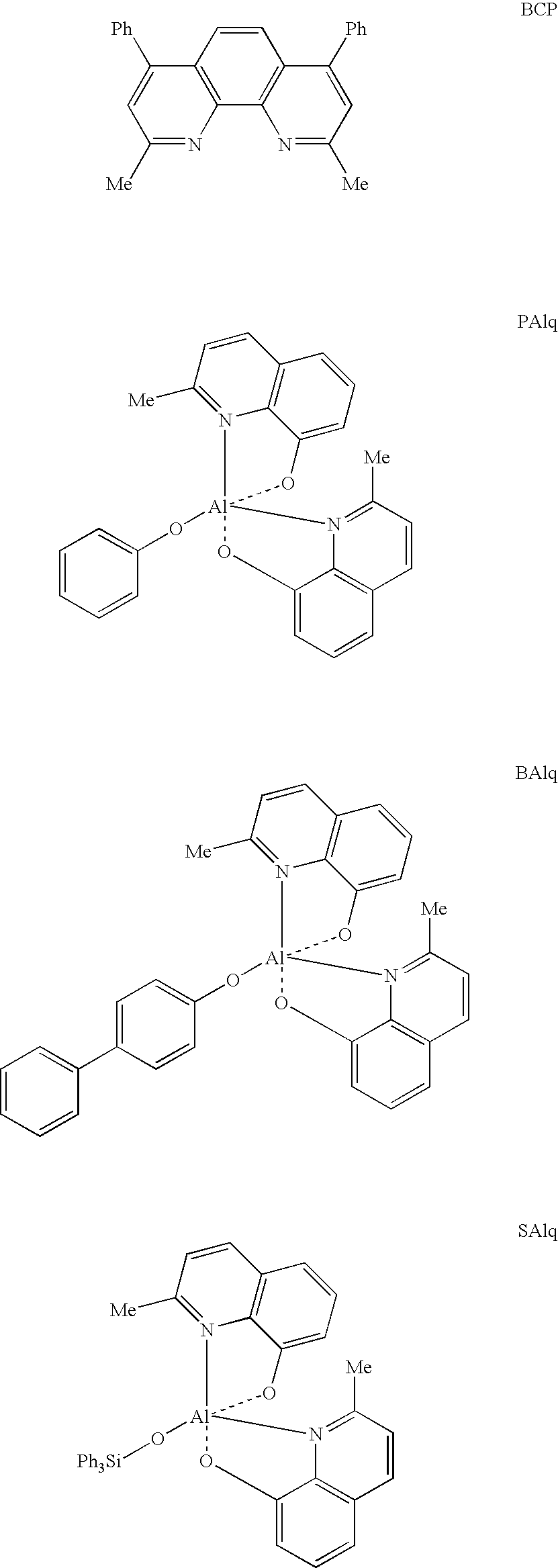
- a hole blocking modification layer of the present disclosure can comprise, for example, TPBI as shown in group G4, BCP (2,9-dimethyl-4,7-diphenyl-1,10-phenanthroline), BAlq (aluminum[III]bis[2-methyl-8-quinolinato][4-phenylphenolate]), PAlq (aluminum[III]bis[2-methyl-8-quinolinato]-[4-phenolate]), or SAlq (aluminum[III]bis[2-methyl-8-quinolinato][triphenylsilanolate]) which has the Formula shown in group G5.
- BCP 2,9-dimethyl-4,7-diphenyl-1,10-phenanthroline
- BAlq aluminum[III]bis[2-methyl-8-quinolinato][4-phenylphenolate]
- PAlq aluminum[III]bis[2-methyl-8-quinolinato]-[4-phenolate]
- SAlq aluminum[III]
- electron-transporting materials examples include TPBI, TAZ-1, TAZ-2, TAZ-3, PBD shown in group G4, Alq 3 (tris[8-hydroxyquinolinato]aluminum), DPA (4,7-diphenyl-1,10-phenanthroline) which has the Formula shown in group G5, and TYE704 (commercially available from Toyo Ink).
- Ph represents a phenyl group
- Me represents a methyl group
- Et represents an ethyl group
- Bu represents a butyl group.
- Embodiments of the present disclosure can be further defined by reference to the following examples, which describe in detail preparation of iridium compounds and light-emitting elements of the present disclosure and procedures for characterizing iridium compounds and light-emitting elements of the present disclosure. It will be apparent to those skilled in the art that many modifications, both to materials and methods, may be practiced without departing from the scope of the present disclosure.
- cd/m 2 brightness, luminance efficiency, candela per square meter
- ITO indium tin oxide
- Example 1 Mpb obtained in Example 1 was used as the ligand (L) to produce the title complex II-1 in a yield of 76% according to the detailed steps described in Example 13.
- the X-ray structure of complex II-1 is shown in FIG. 2 .
- the UV absorption spectrum and the phosphorescence emission spectrum of complex II-1 in dichloromethane are shown in FIG. 3 .
- the complex II-1 emits a green light having a peak wavelength of 510 nm.
- Epb obtained in Example 2 was used as the ligand (L) to produce the title complex II-2 in a yield of 71 % according to the detailed steps described in Example 13.
- the UV absorption spectrum and the phosphorescence emission spectrum of complex II-2 in dichloromethane are shown in FIG. 4 .
- the complex II-2 emits a green light having a peak wavelength of 510 nm.
- the complex II-3 emits a green light having a peak wavelength of 518 nm.
- 1 H NMR (CDCl 3 , ⁇ ): 1.86 (s, 6 H), 5.27 (s, 1 H), 6.58–6.44 (m, 8 H), 7.32–7.26 (m, 4 H), 7.66–7.57 (m, 12 H), 7.77–7.72 (m, 2 H).
- Example 4 Bpb obtained in Example 4 was used as the ligand (L) to produce the title complex II-4 in a yield of 75% according to the detailed steps described in Example 13.
- the UV absorption spectrum and the phosphorescence emission spectrum of complex II-4 in dichloromethane are shown in FIG. 6 .
- the complex II-4 emits a green light having a peak wavelength of 516 nm.
- Example 5 Dfbpb obtained in Example 5 was used as the ligand (L) to produce the title complex II-5 according to the detailed steps described in Example 13.
- the UV absorption spectrum and the phosphorescence emission spectrum of the complex II-5 in dichloromethane are shown in FIG. 7 .
- the complex II-5 emits a blue-green light having a peak wavelength of 496 nm.
- MObpb obtained in Example 6 was used as the ligand (L) to produce the title complex II-6 in a yield of 83% according to the detailed steps described in Example 13.
- the UV absorption spectrum and the phosphorescence emission spectrum of the complex II-6 in dichloromethane are shown in FIG. 8 .
- the complex II-6 emits a blue-green light having a wavelength of 496 nm.
- Example 7 Mbpb obtained in Example 7 was used as the ligand (L) to produce the title complex II-7 in a yield of 80% according to the detailed steps described in Example 13.
- the UV absorption spectrum and the phosphorescence emission spectrum of the complex II-7 in dichloromethane are shown in FIG. 9 .
- the complex II-7 emits a green light having a peak wavelength of 508 nm.
- Tbtpb obtained in Example 8 was used as the ligand (L) to produce the title complex II-8 according to the detailed steps described in Example 13.
- Example 9 Dfppb obtained in Example 9 was used as the ligand (L) instead of Dpb to produce the title complex II-10 in a yield of 83% according to the detailed steps described in Example 16.
- the X-ray structure of the complex II-10 is shown in FIG. 10 .
- the UV absorption spectrum and the phosphorescence emission spectrum of complex II-10 in dichloromethane are shown in FIG. 11 .
- the complex II-10 emits a green light having a peak wavelength of 502 nm.
- Example 10 Fppb obtained in Example 10 was used as the ligand (L) instead of Dpb to produce the title complex II-11 in a yield of 74% according to the detailed steps described in Example 16.
- the UV absorption spectrum and the phosphorescence emission spectrum of the complex II-11 in dichloromethane are shown in FIG. 12 .
- the complex II-11 emits a green light having a peak wavelength of 504 nm.
- Example 11 Ptpb obtained in Example 11 was used as the ligand (L) instead of Dpb to produce the complex II-12 in a yield of 92% according to the detailed steps described in Example 16.
- the UV absorption spectrum and the phosphorescence emission spectrum of the complex II-12 in dichloromethane are shown in FIG. 13 .
- the complex II-12 emits a green light having a peak wavelength of 536 nm.
- Example 12 Bdmpb obtained in Example 12 was used as the ligand (L) to produce the title complex II-13 in a yield of 83% according to the detailed steps described in Example 13.
- the UV absorption spectrum and the phosphorescence emission spectrum of the complex II-13 in dichloromethane are shown in FIG. 14 .
- the complex II-11 emits a green light having a peak wavelength of 514 nm.
- a hole injection modification layer has a thickness ranging from about 10 to about 35 nanometers. In certain embodiments, a hole transporting layer has a thickness ranging from about 10 to about 50 nanometers.
- a hole blocking layer has a thickness ranging from about 10 to about 20 nanometers.
- a electron transporting layer has a thickness ranging from about 10 to about 50 nanometers.
- an election injection layer such as potassium fluoride, has a thickness of about 0.5 nanometer.
- the deposition rate was about 5 angstroms per second, and the thickness of the deposited cathode layer ranged from about 10 to about 55 nanometers.
- the layer when silver was deposited and aromatic amine (such as 2-TNATA or IDE320 was deposited as a protection layer, the layer had a thickness ranging from about 30 to about 150 nanometers.
- Certain device configurations are set forth in Examples 25–51, and corresponding characteristics are provided in Table 1.
- the composition and thickness of the layers comprising a device are provided in the following order: anode layer//hole injection layer///light emitting layer//hole blocking layer//electron transport layer//and cathode layer.
- ITO//NPB (50 nm)//II-1: CBP (7.3%, 30 nm)//BCP (10 nm)//Alq (40 nm)//Mg:Ag 10:1.
- ITO//NPB (50 nm)//II-1: TCTA (6.3%, 30 nm)//BCP (10 nm)//Alq (40 nm)//Mg:Ag 10:1.
- ITO//TCTA (30 nm)//II-1: TCTA (6.3%, 30 nm)//BCP (10 nm)//Alq (40 nm)//Mg:Ag 10:1.
- ITO//NPB (30 nm)//II-2: CBP (7.3%, 30 nm)//BCP (10 nm)//Alq.(40 nm)//Mg:Ag 10:1.
- ITO//TCTA (30 nm)//II-2: CBP (7%, 30 nm)//BCP (10 nm)//Alq (40 nm)//Mg:Ag 10:1.
- ITO//NPB (50 nm)//II-3: CBP (7%, 30 nm)//BCP (10 nm)//Alq (40 nm)//Mg:Ag 10:1.
- ITO//NPB (30 nm)//II-3: CBP (9%, 30 nm)//BCP (10 nm)//Alq (40 nm)//Mg:Ag 10:1.
- ITO//TCTA (30 nm)//II-3: TCTA (6.7%, 30 nm)//BCP (10 nm)//Alq (40 nm)//Mg:Ag 10:1.
- ITO//TCTA (30 nm)//II-3: CBP (6.3%, 30 nm)//BCP (10 nm)//Alq (40 nm)//Mg:Ag 10:1.
- ITO//CuPc (10 nm)//NPB (30 nm)//II-3: CBP (5.7%, 30 nm)//BCP (10 nm)//Alq (40 nm)//Mg:Ag 10:1.
- ITO//TCTA (30 nm)//II-3: CBP (7%, 30 nm)//BAlq (30 nm)//Mg:Ag 10:1.
- Al/Ni/NiO//IDE406 35 nm)//IDE320 (10 nm)//II-3: TMM004 (7%, 25 nm)//BAlq (10 nm)//TYE704 (20 nm)//Ca (15 nm)//Mg (8 nm)//IDE320 (50 nm).
- ITO//NPB (50 nm)//II-4: CBP (4.7%, 30 nm)//BCP (10 nm)//Alq (40 nm)//Mg:Ag 10:1.
- ITO//NPB (50 nm)//II-4: CBP (6.7%, 30 nm)//BCP (10 nm)//Alq (40 nm)//Mg:Ag 10:1.
- ITO//NPB (50 nm)//II-4: CBP (8.7%, 30 nm)//BCP (10 nm)//Alq (40 nm)//Mg:Ag 10:1.
- ITO//NPB (50 nm)//II-4: TCTA (7%, 30 nm)//BCP (10 nm)//Alq (40 nm)//Mg:Ag 10:1.
- ITO//NPB (30 nm)//TCTA (20 nm)//II-4: TCTA (7%, 30 nm)//BCP (10 nm)//Alq (40 nm)//Mg:Ag 10:1.
- ITO//NPB (30 nm)//II-5: CCP (9.7%, 30 nm)//BCP (10 nm)//Alq (40 nm)//Mg:Ag 10:1.
- ITO//m-MTDATA (30 nm)//II-5: CCP (10.3%, 30 nm)//BCP (10 nm)//Alq (40 nm)//Mg:Ag 10:1.
- ITO//TCTA (30 nm)//II-5: TCB (6.3%, 30 nm)//BCP (10 nm)//Alq (40 nm)//Mg:Ag 10:1.
- ITO//TCTA (30 nm)//II-10: CBP (7%, 30 nm)//BCP (10 nm)//Alq (40 nm)//Mg:Ag 10:1.
- ITO//TCTA (30 nm)//II-11: CBP (6.7%, 30 nm)//BCP (10 nm)//Alq (40 nm)//Mg:Ag 10:1.
- ITO//NPB (50 nm)//II-13: CBP (7%, 30 nm)//BCP (10 nm)//Alq (40 nm)//Mg:Ag 10:1.
- the phosphorescent iridium complexes disclosed in the present disclosure are suitable for use in forming an OLED device.
- An OLED device formed using the phosphorescent iridium complexes of the present disclosure can emit light having a color ranging from blue-green through green, high brightness, high current efficiency, and excellent CIE coordinates.
- a wavelength ranging from about 470 nm to about 570 nm corresponds to the blue-green to green region of the electromagnetic spectrum.
- an OLED device comprising at least one phosphorescent iridium complex of the disclosure emits light having a peak wavelength ranging from about 490 nm to 530 mn.
Abstract

wherein X is chosen from a monoanionic bidentate ligand; Z is chosen from an atomic group wherein Z together with the buta-1,3-diene to which Z is attached form an aryl group or heteroaryl group; R, R1, and R2 are independently chosen from a hydrogen atom or a substituent; m is an integer from 0 to 4; and n is an integer from 0 to the maximum number of possible substituents on Z, are disclosed. Light emitting devices using the phosphorescent iridium complexes are also disclosed.
Description


give the title compound.
| TABLE 1 | ||||||
| External | Maximum | Peak | CIE | Peak | ||
| Voltage | Quantum | Brightness | Efficiency | Coordinates | Wavelength | |
| Example | (V) | Efficiency (%) | (cd/m2 (V)) | (cd/A (V)) | (8 V) (x, y) | λmax (nm) |
| 27 | 3.1 | 11.10 (7.5) | 100126 (14.0) | 40.85 (7.5) | (0.24, 0.66) | 512 |
| 28 | 2.9 | 9.38 (8.0) | 98799 (13.0) | 35.29 (8.0) | (0.27, 0.64) | 514 |
| 29 | 2.8 | 10.66 (6.0) | 89343 (13.0) | 39.59 (6.0) | (0.26, 0.65) | 512 |
| 30 | 2.7 | 9.14 (6.5) | 72045 (12.5) | 33.73 (6.5) | (0.26, 0.64) | 512 |
| 31 | 3.0 | 9.54 (6.5) | 101622 (13.0) | 35.89 (6.5) | (0.27, 0.65) | 514 |
| 32 | 2.7 | 7.88 (7.5) | 105202 (13.0) | 29.58 (7.5) | (0.28, 0.64) | 514 |
| 33 | 3.0 | 14.69 (6.0) | 140407 (14.5) | 57.44 (6.0) | (0.30, 0.64) | 520 |
| 34 | 2.7 | 11.71 (6.5) | 130455 (13.5) | 45.29 (6.5) | (0.31, 0.63) | 520 |
| 35 | 2.7 | 7.58 (5.5) | 65773 (11.5) | 29.21 (5.5) | (0.29, 0.64) | 520 |
| 36 | 3.0 | 10.50 (7.0) | 143374 (13.5) | 41.17 (7.0) | (0.31, 0.64) | 522 |
| 37 | 2.7 | 13.46 (7.5) | 136208 (14.5) | 52.61 (7.5) | (0.31, 0.64) | 522 |
| 38 | 3.5 | 15.53 (7.5) | 119615 (17.5) | 61.77 (7.5) | (0.30, 0.65) | 522 |
| 39 | 4.5 | 4.54 (8.5) | 66466 (13.5) | 17.77 (8.5) | (0.32, 0.63) | 520 |
| 40 | 2.5 | 15.86 (3.5) | 56140 (10.0) | 63.11 (3.5) | (0.35, 0.61) | 525 |
| 41 | 3.0 | 11.02 (8.0) | 88080 (14.5) | 42.10 (8.0) | (0.29, 0.64) | 516 |
| 42 | 2.8 | 14.02 (7.5) | 114309 (14.0) | 54.73 (7.5) | (0.30, 0.64) | 518 |
| 43 | 2.8 | 11.89 (8.5) | 104291 (14.0) | 46.10 (8.5) | (0.29, 0.65) | 516 |
| 44 | 2.7 | 10.15 (5.5) | 62776 (12.0) | 38.52 (5.5) | (0.27, 0.65) | 514 |
| 45 | 3.1 | 9.61 (7.5) | 70540 (12.5) | 36.76 (7.5) | (0.28, 0.65) | 516 |
| 46 | 3.9 | 3.77 (8.0) | 17614 (12.5) | 12.61 (8.0) | (0.26, 0.57) | 496 |
| 47 | 4.1 | 4.73 (8.5) | 16769 (15.5) | 15.74 (8.5) | (0.24, 0.57) | 496 |
| 48 | 3.7 | 5.04 (8.0) | 19111 (12.5) | 16.29 (8.0) | (0.23, 0.57) | 494 |
| 49 | 4.5 | 4.29 (8.5) | 13610 (12.0) | 13.72 (8.5) | (0.23, 0.58) | 498 |
| 50 | 3.7 | 10.44 (9.0) | 47584 (13.0) | 34.91 (9.0) | (0.23, 0.60) | 502 |
| 51 | 2.8 | 9.37 (8.0) | 58180 (13.2) | 36.89 (8.0) | (0.31, 0.64) | 520 |
Claims (39)


Applications Claiming Priority (2)
| Application Number | Priority Date | Filing Date | Title |
|---|---|---|---|
| TW092132297 | 2003-11-18 | ||
| TW092132297A TWI245068B (en) | 2003-11-18 | 2003-11-18 | Iridium complex as light emitting material and organic light emitting diode device |
Publications (2)
| Publication Number | Publication Date |
|---|---|
| US20050116626A1 US20050116626A1 (en) | 2005-06-02 |
| US7193088B2 true US7193088B2 (en) | 2007-03-20 |
Family
ID=34617986
Family Applications (1)
| Application Number | Title | Priority Date | Filing Date |
|---|---|---|---|
| US10/992,594 Active 2025-05-28 US7193088B2 (en) | 2003-11-18 | 2004-11-17 | Iridium complexes as light emitting materials and organic light emitting diode device |
Country Status (3)
| Country | Link |
|---|---|
| US (1) | US7193088B2 (en) |
| JP (1) | JP4543136B2 (en) |
| TW (1) | TWI245068B (en) |
Cited By (18)
| Publication number | Priority date | Publication date | Assignee | Title |
|---|---|---|---|---|
| US20090062542A1 (en) * | 2007-07-24 | 2009-03-05 | Gracel Display Inc. | Novel red electroluminescent compounds and organic electroluminescent device using the same |
| US20090078317A1 (en) * | 2007-09-07 | 2009-03-26 | Gracel Display Inc. | Organometalic compounds for electroluminescence and organic electroluminescent device using the same |
| US20090149653A1 (en) * | 2007-12-03 | 2009-06-11 | Chien-Hong Cheng | Transition metal complexes with carbene ligands and their application |
| US20090145483A1 (en) * | 2007-11-12 | 2009-06-11 | Gracel Display Inc. | Novel electroluminescent compounds and organic electroluminescent device suing the same |
| US20090153040A1 (en) * | 2007-11-22 | 2009-06-18 | Gracel Display Inc. | Novel organic electroluminescent compounds and organic electroluminescent device using the same |
| US20090159130A1 (en) * | 2007-11-20 | 2009-06-25 | Gracel Display Inc. | Novel organic electroluminescent compounds and organic electroluminescent device using the same |
| US20090165860A1 (en) * | 2007-12-31 | 2009-07-02 | Gracel Display Inc. | Electroluminescent device using electroluminescent compounds |
| US20090174316A1 (en) * | 2007-11-02 | 2009-07-09 | Gracel Display Inc. | Novel red electroluminescent compounds and organi electroluminescent device using the same |
| US20090179555A1 (en) * | 2007-11-20 | 2009-07-16 | Gracel Display Inc. | Novel red electroluminescent compounds and organic electroluminescent device using the same |
| US20090184631A1 (en) * | 2007-11-27 | 2009-07-23 | Gracel Display Inc. | Novel red electroluminescent compounds and organic electroluminescent device using the same |
| US20090189520A1 (en) * | 2007-07-24 | 2009-07-30 | Gracel Display Inc. | Novel red electroluminescent compounds and organic electroluminescent device using the same |
| US20090252990A1 (en) * | 2007-11-15 | 2009-10-08 | Gracel Display Inc. | Novel organic electroluminescent compounds and organic electroluminescent device using the same |
| US20090261714A1 (en) * | 2008-01-29 | 2009-10-22 | Gracel Display Inc. | Novel organic electroluminescent compounds and organic electroluminescent device using the same |
| US20090295281A1 (en) * | 2008-02-29 | 2009-12-03 | Gracel Display Inc. | Novel organic electroluminescent compounds and organic electroluminescent device using the same |
| US20100102710A1 (en) * | 2008-03-19 | 2010-04-29 | Gracel Display Inc. | Novel organic electroluminescent compounds and organic electroluminescent device using the same |
| US20100141127A1 (en) * | 2008-11-11 | 2010-06-10 | Universal Display Corporation | Phosphorescent emitters |
| US20100141133A1 (en) * | 2005-11-25 | 2010-06-10 | Chi Mei Optoelectronics Corp. | Light-emitting element and iridium complex |
| US20100152455A1 (en) * | 2007-01-04 | 2010-06-17 | Gracel Display Inc. | Organometalic compounds for electroluminescence and organic electroluminescent device using the same |
Families Citing this family (31)
| Publication number | Priority date | Publication date | Assignee | Title |
|---|---|---|---|---|
| JP4203732B2 (en) * | 2003-06-12 | 2009-01-07 | ソニー株式会社 | Organic electroluminescent material, organic electroluminescent element, and heterocyclic iridium complex compound |
| JP5000497B2 (en) * | 2004-06-30 | 2012-08-15 | メルク パテント ゲゼルシャフト ミット ベシュレンクテル ハフツング | Electroluminescent materials and devices |
| KR100721562B1 (en) * | 2004-12-03 | 2007-05-23 | 삼성에스디아이 주식회사 | Organic light emitting device having cathode of magnesium-calcium layer and fabrication method of the same |
| US7902374B2 (en) * | 2005-05-06 | 2011-03-08 | Universal Display Corporation | Stability OLED materials and devices |
| US9051344B2 (en) * | 2005-05-06 | 2015-06-09 | Universal Display Corporation | Stability OLED materials and devices |
| GB2475647B (en) * | 2005-06-09 | 2011-07-13 | Konica Minolta Holdings Inc | Organic electroluminescent element, illuminator and display |
| GB2442885B (en) | 2005-06-09 | 2011-07-13 | Konica Minolta Holdings Inc | Organic electroluminescence element, illuminator and display |
| JPWO2007026581A1 (en) * | 2005-08-30 | 2009-03-05 | 出光興産株式会社 | Organic electroluminescence device |
| WO2007029461A1 (en) * | 2005-09-02 | 2007-03-15 | Konica Minolta Holdings, Inc. | Organic electroluminescent device, method for manufacturing same, display comprising such organic electroluminescent device, and illuminating device |
| KR100747572B1 (en) * | 2005-11-07 | 2007-08-08 | 엘지전자 주식회사 | Red phosphorescene compounds and organic electroluminescence devices using the same |
| JP2007179828A (en) * | 2005-12-27 | 2007-07-12 | Fujifilm Corp | Organic electroluminescent element and method of manufacturing same |
| KR100684109B1 (en) * | 2006-01-24 | 2007-02-16 | (주)그라쎌 | Electroluminescent compounds and organic electroluminescent device using the same |
| EP1878724A1 (en) * | 2006-07-15 | 2008-01-16 | sanofi-aventis | A regioselective palladium catalyzed synthesis of benzimidazoles and azabenzimidazoles |
| US8852757B2 (en) | 2006-09-08 | 2014-10-07 | Konica Minolta Holdings, Inc. | Organic electroluminescence element, lighting device and display device |
| US8062767B2 (en) * | 2007-03-06 | 2011-11-22 | Chien-Hong Cheng | Organic light emitting diode containing a Ir complex having a novel ligand as a phosphorescent emitter |
| JP5242976B2 (en) * | 2007-09-03 | 2013-07-24 | 日本放送協会 | Organic electroluminescence device |
| WO2009060779A1 (en) * | 2007-11-08 | 2009-05-14 | Konica Minolta Holdings, Inc. | Organic electroluminescent device material, organic electroluminescent device, display device and illuminating device |
| CN103107284A (en) * | 2007-12-28 | 2013-05-15 | 出光兴产株式会社 | Aromatic amine derivative and organic electroluminescent element using the same |
| KR100952966B1 (en) * | 2007-12-31 | 2010-04-15 | 제일모직주식회사 | Organometallic complex compounds for photoelectric device and photoelectric device comprising the same |
| WO2011024737A1 (en) | 2009-08-27 | 2011-03-03 | 独立行政法人産業技術総合研究所 | Iridium complex and light emitting material formed from same |
| JP5688930B2 (en) | 2009-08-27 | 2015-03-25 | 住友化学株式会社 | Metal complex composition and complex polymer |
| KR20110120016A (en) * | 2010-04-28 | 2011-11-03 | 삼성모바일디스플레이주식회사 | Organic light emitting device |
| WO2012005045A1 (en) * | 2010-07-06 | 2012-01-12 | シャープ株式会社 | Illumination device and manufacturing method thereof |
| CN102659846B (en) * | 2012-03-30 | 2015-07-15 | 中国科学院宁波材料技术与工程研究所 | N-substituted phenylbenzimidazole trivalent-iridium organometallic complex and its preparation method and use |
| WO2015061074A1 (en) * | 2013-10-25 | 2015-04-30 | E. I. Du Pont De Nemours And Company | Electronic device including a fluoranthene derivative |
| CN104744450A (en) * | 2013-12-26 | 2015-07-01 | 东丽先端材料研究开发(中国)有限公司 | Aromatic amine compound, light emitting element material and light emitting element |
| CN106146568A (en) * | 2015-04-23 | 2016-11-23 | 上海和辉光电有限公司 | A kind of compound and its preparation method and application |
| CN110088115A (en) * | 2016-12-16 | 2019-08-02 | 株式会社半导体能源研究所 | Organometallic complex, light-emitting component, light emitting device, electronic device and lighting device |
| CN112209973B (en) * | 2020-11-05 | 2022-06-24 | 北京燕化集联光电技术有限公司 | Oxygen-containing organic electrophosphorescent material and application thereof |
| CN112175017B (en) * | 2020-11-05 | 2022-06-14 | 北京燕化集联光电技术有限公司 | Organic electrophosphorescent material and application thereof |
| US20230133787A1 (en) * | 2021-06-08 | 2023-05-04 | University Of Southern California | Molecular Alignment of Homoleptic Iridium Phosphors |
Citations (4)
| Publication number | Priority date | Publication date | Assignee | Title |
|---|---|---|---|---|
| US6687266B1 (en) | 2002-11-08 | 2004-02-03 | Universal Display Corporation | Organic light emitting materials and devices |
| US20050008895A1 (en) * | 2003-06-12 | 2005-01-13 | Ichinori Takada | Organic electroluminescent material, organic electroluminescent device, and heterocycle-containing iridium complex compound |
| US6936716B1 (en) * | 2004-05-17 | 2005-08-30 | Au Optronics Corp. | Organometallic complex for organic electroluminescent device |
| US20060008670A1 (en) * | 2004-07-06 | 2006-01-12 | Chun Lin | Organic light emitting materials and devices |
Family Cites Families (2)
| Publication number | Priority date | Publication date | Assignee | Title |
|---|---|---|---|---|
| JP4039023B2 (en) * | 2000-10-04 | 2008-01-30 | 三菱化学株式会社 | Organic electroluminescence device |
| JP4192592B2 (en) * | 2001-12-26 | 2008-12-10 | 三菱化学株式会社 | Organic iridium complex and organic electroluminescent device using the same |
-
2003
- 2003-11-18 TW TW092132297A patent/TWI245068B/en not_active IP Right Cessation
-
2004
- 2004-11-16 JP JP2004332143A patent/JP4543136B2/en not_active Expired - Fee Related
- 2004-11-17 US US10/992,594 patent/US7193088B2/en active Active
Patent Citations (4)
| Publication number | Priority date | Publication date | Assignee | Title |
|---|---|---|---|---|
| US6687266B1 (en) | 2002-11-08 | 2004-02-03 | Universal Display Corporation | Organic light emitting materials and devices |
| US20050008895A1 (en) * | 2003-06-12 | 2005-01-13 | Ichinori Takada | Organic electroluminescent material, organic electroluminescent device, and heterocycle-containing iridium complex compound |
| US6936716B1 (en) * | 2004-05-17 | 2005-08-30 | Au Optronics Corp. | Organometallic complex for organic electroluminescent device |
| US20060008670A1 (en) * | 2004-07-06 | 2006-01-12 | Chun Lin | Organic light emitting materials and devices |
Non-Patent Citations (1)
| Title |
|---|
| Huang et al., Chemistry of Materials, 16(12), 2480-2488, 2004. * |
Cited By (22)
| Publication number | Priority date | Publication date | Assignee | Title |
|---|---|---|---|---|
| US20100141133A1 (en) * | 2005-11-25 | 2010-06-10 | Chi Mei Optoelectronics Corp. | Light-emitting element and iridium complex |
| US8586201B2 (en) | 2005-11-25 | 2013-11-19 | Chimei Innolux Corporation | Light-emitting element and iridium complex |
| US20100152455A1 (en) * | 2007-01-04 | 2010-06-17 | Gracel Display Inc. | Organometalic compounds for electroluminescence and organic electroluminescent device using the same |
| US7723520B2 (en) | 2007-07-24 | 2010-05-25 | Skc Haas Display Films Co., Ltd. | Red electroluminescent compounds and organic electroluminescent device using the same |
| US20090189520A1 (en) * | 2007-07-24 | 2009-07-30 | Gracel Display Inc. | Novel red electroluminescent compounds and organic electroluminescent device using the same |
| US20090062542A1 (en) * | 2007-07-24 | 2009-03-05 | Gracel Display Inc. | Novel red electroluminescent compounds and organic electroluminescent device using the same |
| US20090078317A1 (en) * | 2007-09-07 | 2009-03-26 | Gracel Display Inc. | Organometalic compounds for electroluminescence and organic electroluminescent device using the same |
| US20090174316A1 (en) * | 2007-11-02 | 2009-07-09 | Gracel Display Inc. | Novel red electroluminescent compounds and organi electroluminescent device using the same |
| US20090145483A1 (en) * | 2007-11-12 | 2009-06-11 | Gracel Display Inc. | Novel electroluminescent compounds and organic electroluminescent device suing the same |
| US20090252990A1 (en) * | 2007-11-15 | 2009-10-08 | Gracel Display Inc. | Novel organic electroluminescent compounds and organic electroluminescent device using the same |
| US20090179555A1 (en) * | 2007-11-20 | 2009-07-16 | Gracel Display Inc. | Novel red electroluminescent compounds and organic electroluminescent device using the same |
| US20090159130A1 (en) * | 2007-11-20 | 2009-06-25 | Gracel Display Inc. | Novel organic electroluminescent compounds and organic electroluminescent device using the same |
| US20090153040A1 (en) * | 2007-11-22 | 2009-06-18 | Gracel Display Inc. | Novel organic electroluminescent compounds and organic electroluminescent device using the same |
| US20090184631A1 (en) * | 2007-11-27 | 2009-07-23 | Gracel Display Inc. | Novel red electroluminescent compounds and organic electroluminescent device using the same |
| US7960547B2 (en) * | 2007-12-03 | 2011-06-14 | Chien-Hong Cheng | Transition metal complexes with carbene ligands and their application |
| US20090149653A1 (en) * | 2007-12-03 | 2009-06-11 | Chien-Hong Cheng | Transition metal complexes with carbene ligands and their application |
| US20090165860A1 (en) * | 2007-12-31 | 2009-07-02 | Gracel Display Inc. | Electroluminescent device using electroluminescent compounds |
| US20090261714A1 (en) * | 2008-01-29 | 2009-10-22 | Gracel Display Inc. | Novel organic electroluminescent compounds and organic electroluminescent device using the same |
| US20090295281A1 (en) * | 2008-02-29 | 2009-12-03 | Gracel Display Inc. | Novel organic electroluminescent compounds and organic electroluminescent device using the same |
| US20100102710A1 (en) * | 2008-03-19 | 2010-04-29 | Gracel Display Inc. | Novel organic electroluminescent compounds and organic electroluminescent device using the same |
| US20100141127A1 (en) * | 2008-11-11 | 2010-06-10 | Universal Display Corporation | Phosphorescent emitters |
| US8367223B2 (en) * | 2008-11-11 | 2013-02-05 | Universal Display Corporation | Heteroleptic phosphorescent emitters |
Also Published As
| Publication number | Publication date |
|---|---|
| TWI245068B (en) | 2005-12-11 |
| TW200517470A (en) | 2005-06-01 |
| JP4543136B2 (en) | 2010-09-15 |
| US20050116626A1 (en) | 2005-06-02 |
| JP2005163036A (en) | 2005-06-23 |
Similar Documents
| Publication | Publication Date | Title |
|---|---|---|
| US7193088B2 (en) | Iridium complexes as light emitting materials and organic light emitting diode device | |
| KR101577468B1 (en) | Use of acridine derivatives as matrix materials and/or an electron blocker in oleds | |
| JP5256484B2 (en) | ORGANIC ELECTROLUMINESCENT ELEMENT, ORGANIC ELECTROLUMINESCENT ELEMENT MATERIAL, DISPLAY DEVICE AND LIGHTING DEVICE | |
| CN102603803B (en) | The electroluminescent stability improved | |
| US7332233B2 (en) | Iridium compound and organic electroluminescent device using the same | |
| CN111732611B (en) | Novel tetradentate platinum complexes | |
| US8586201B2 (en) | Light-emitting element and iridium complex | |
| EP2770036B1 (en) | Material for organic electroluminescent devices and organic electroluminescent devices made by using the same | |
| JP5076900B2 (en) | Organic electroluminescence element, display device and lighting device | |
| EP2271183B1 (en) | Organic electroluminescent element, display and illuminator | |
| US7915409B2 (en) | Organometal complex and light-emitting element using the same | |
| JP4976288B2 (en) | Organometallic complex and organic electroluminescence device using the same | |
| US7709100B2 (en) | Electroluminescent efficiency | |
| JP4300902B2 (en) | Block copolymer, organic electroluminescence element, display device, lighting device and light source | |
| JPWO2005097940A1 (en) | ORGANIC ELECTROLUMINESCENT ELEMENT MATERIAL, ORGANIC ELECTROLUMINESCENT ELEMENT, DISPLAY DEVICE AND LIGHTING DEVICE | |
| JP2011029647A (en) | Organic electroluminescent device | |
| WO2006013738A1 (en) | Organic electroluminescence device, display apparatus and lighting apparatus | |
| JP2002343572A (en) | Light-emitting element and display device employing porphyrin derivative compound | |
| JP2005314663A (en) | Organic electroluminescent element material, organic electroluminescent element, display device and illuminating apparatus | |
| KR20050014708A (en) | Light-emitting element and iridium complex | |
| JP4935001B2 (en) | Organic electroluminescence element material | |
| US7320834B2 (en) | Organic light emitting diode containing a novel Ir complex as a phosphorescent emitter | |
| TWI242999B (en) | Organometallic compound and organic electroluminescent device including the same | |
| JP4904727B2 (en) | ORGANIC ELECTROLUMINESCENT ELEMENT MATERIAL, ORGANIC ELECTROLUMINESCENT ELEMENT, DISPLAY DEVICE AND LIGHTING DEVICE | |
| KR101546089B1 (en) | Organic thin film Materials for Organic Electroluminescent Device and Organic Electroluminescent Device |
Legal Events
| Date | Code | Title | Description |
|---|---|---|---|
| AS | Assignment |
Owner name: CHI MEI OPTOELECTRONICS, TAIWAN Free format text: ASSIGNMENT OF ASSIGNORS INTEREST;ASSIGNORS:CHENG, CHIEN-HONG;CHEN, RUEY-MIN;GUO, HONG-RU;AND OTHERS;REEL/FRAME:015648/0461;SIGNING DATES FROM 20050202 TO 20050204 Owner name: NATIONAL TSING HUA UNIVERSITY, TAIWAN Free format text: ASSIGNMENT OF ASSIGNORS INTEREST;ASSIGNORS:CHENG, CHIEN-HONG;CHEN, RUEY-MIN;GUO, HONG-RU;AND OTHERS;REEL/FRAME:015648/0461;SIGNING DATES FROM 20050202 TO 20050204 |
|
| STCF | Information on status: patent grant |
Free format text: PATENTED CASE |
|
| AS | Assignment |
Owner name: CHIMEI INNOLUX CORPORATION,TAIWAN Free format text: MERGER;ASSIGNOR:CHI MEI OPTOELECTRONICS CORP;REEL/FRAME:024358/0255 Effective date: 20100318 Owner name: CHIMEI INNOLUX CORPORATION, TAIWAN Free format text: MERGER;ASSIGNOR:CHI MEI OPTOELECTRONICS CORP;REEL/FRAME:024358/0255 Effective date: 20100318 |
|
| FPAY | Fee payment |
Year of fee payment: 4 |
|
| AS | Assignment |
Owner name: INNOLUX CORPORATION, TAIWAN Free format text: CHANGE OF NAME;ASSIGNOR:CHIMEI INNOLUX CORPORATION;REEL/FRAME:032604/0487 Effective date: 20121219 |
|
| FPAY | Fee payment |
Year of fee payment: 8 |
|
| MAFP | Maintenance fee payment |
Free format text: PAYMENT OF MAINTENANCE FEE, 12TH YEAR, LARGE ENTITY (ORIGINAL EVENT CODE: M1553); ENTITY STATUS OF PATENT OWNER: LARGE ENTITY Year of fee payment: 12 |