US7207016B2 - Method for classifying errors in the layout of a semiconductor circuit - Google Patents
Method for classifying errors in the layout of a semiconductor circuit Download PDFInfo
- Publication number
- US7207016B2 US7207016B2 US10/447,386 US44738603A US7207016B2 US 7207016 B2 US7207016 B2 US 7207016B2 US 44738603 A US44738603 A US 44738603A US 7207016 B2 US7207016 B2 US 7207016B2
- Authority
- US
- United States
- Prior art keywords
- error
- layout
- information
- geometrical
- pattern
- Prior art date
- Legal status (The legal status is an assumption and is not a legal conclusion. Google has not performed a legal analysis and makes no representation as to the accuracy of the status listed.)
- Expired - Fee Related, expires
Links
Images


Classifications
-
- G—PHYSICS
- G06—COMPUTING; CALCULATING OR COUNTING
- G06F—ELECTRIC DIGITAL DATA PROCESSING
- G06F30/00—Computer-aided design [CAD]
- G06F30/30—Circuit design
- G06F30/39—Circuit design at the physical level
- G06F30/398—Design verification or optimisation, e.g. using design rule check [DRC], layout versus schematics [LVS] or finite element methods [FEM]
Definitions
- Known physical verification software checks the physical semiconductor circuit design for adherence to defined design rules that are intended, by way of example, to guarantee the manufacturability and operability of the circuit on silicon. For every transgression of a design rule, the software generates an error message that indicates which rule has been transgressed at which point in the circuit. To clarify the transgression, an “error marker” is also produced.
- the error marker can have various forms.
- the manufacturers of verification software take the following model of use as a basis: if a design rule has been transgressed, then this is found by the user on the basis of the error message, is considered and is finally corrected.
- design-rule transgressions are classified by the user as being “irrelevant”, “noncritical” or “acceptable in this instance” and are not corrected.
- the user thus supplies additional knowledge, such as experience relating to the manufacturability of a structure on silicon despite the formal transgression of the design rule.
- the number of errors which are accepted in this manner can run into thousands in repetitive structures such as arise on memory chips, for example.
- error messages exist in unspecified assortment for a design rule transgression and within a cell (large IC designs are divided into a hierarchy of cells) and contain no objectifiable order features.
- the intention is to allow acceptable errors to be distinguished from those that should not be accepted.
- a method for classifying errors in a layout of a semiconductor circuit includes examining the layout of the semiconductor circuit for infringement of predetermined design rules for establishing errors, marking each error in the layout, extracting information about the error and about the layout of the semiconductor circuit in an area surrounding the error resulting in extracted information, comparing the extracted information with prestored information within a multiplicity of classes resulting in compared information, and assigning the error to a respective class on a basis of the compared information.
- the method involves every error being marked and then information about the error marking and the area of layout surrounding the error being stored in the form of a geometrical pattern in a memory.
- the pattern is then compared with already stored patterns to ascertain geometrical identity.
- the advantage of this method is, in particular, that design rule check (DRC) error markers together with their surrounding area can be efficiently compared on an exact geometrical basis with other DRC error markers and their surrounding area and can thus be classified.
- DRC design rule check
- the area surrounding an error marking contains geometrical objects on one or more reference levels. Every such reference level shows information relating to various aspects of the layout, such as geometrical aspects, or else an association between geometrical information and a physical layer in the semiconductor circuit that is to be manufactured.
- the design rule check can relate to the adherence to a minimum distance between elements in various layers of the semiconductor circuit, these being shown in various reference levels.
- Which reference levels are used for checking the design rules depends on the semantics of the check. Which parts of geometrical objects within a level are included in a pattern is determined using a set of rules that is specific to a design rule check and to the respective reference level and describes the region under consideration.
- errors are assigned to the same error class whenever their pattern is identical to the reference pattern for the error class.
- a pattern library is used. If a pattern is not found in the pattern library, then it is a new pattern, which is indicated to the user and is added to the pattern library for further comparisons.
- every classification can involve the location of the occurrence of a pattern together with its error class being stored in a database, so that not just the first occurrence but all instances of an error class are signaled to the user.
- the pattern comparison is particularly efficient in terms of runtime when the pattern data are normalized.
- the type of normalization depends on the nature of the geometrical objects that are to be normalized (e.g. edges, polygons, error markings).
- the normalized error markings and reference levels are disposed in the layout and compared for all patterns in the order of the reference levels.
- the patterns can therefore be classified by simple geometrical comparison operations.
- the invention also provides a data processing installation for designing the layout of a semiconductor circuit, where the data processing installation is designed for processing layout data for examining the layout design for errors, for extracting a data record which contains information about an error and the layout of the semiconductor circuit in an area surrounding the error, for comparing the information in the extracted data record with prestored information within a multiplicity of classes, and for storing the data record in a memory area associated with the respective class on the basis of the comparison.
- the step of forming the extracted information about the error and the layout of the semiconductor circuit in the area surrounding the error to be geometrical and electrical information.
- the information may represent the error and the layout of the semiconductor circuit in the area surrounding the error as a geometrical pattern, and the prestored information in each of the classes represents a different geometrical pattern.
- a comparison of the information involves the geometrical patterns being compared for geometrical identity.
- the geometrical pattern may contain a number of geometrical objects.
- each of the geometrical objects by a multiplicity of coordinates that are organized according to criteria which are standard for all geometrical objects while maintaining a topology.
- step of representing the layout in a plurality of information levels there is the step of representing the layout in a plurality of information levels, and the information about the layout in the area surrounding the error is associated with at least one of the information levels.
- an order of the information levels are normalized before performing the comparison.
- the step of extracting only the information about the layout in the area surrounding the error that satisfies predetermined criteria is stored in a new class if the extracted information does not match the prestored information in any of the multiplicity of classes.
- the information about a location of the error in the layout and about an associated class is stored when the error is assigned to a class.
- the step of defining the area surrounding the error as a rectangle on the layout there is the step of defining the area surrounding the error as a rectangle on the layout.
- the user defines a size of the rectangle.
- a comparison of the geometrical pattern takes into account all possible geometrical transformations used when designing the layout, resulting in that two compared identical patterns are identified as being identical regardless of possible application of one of the transformations to one of the patterns.
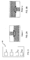
- FIG. 1 is a diagrammatic, plan view of a detail of a layout for a semiconductor circuit
- FIGS. 2A and 2B are plan views of patterns extracted from the semiconductor circuit.
- FIG. 3 is a diagrammatic illustration of a data processing installation for executing computer code.
- the design rules in a production process for integrated circuits prescribe that an overlap between two levels must not be below a prescribed minimum value.
- a physical verification system e.g. “Assura” from the company Cadence Design Systems, Inc. is used to identify transgressions of the rule.
- FIGS. 1 , 2 A, and 2 B thereof there is shown two transgressions of a minimum overlap between two levels 1 and 2 .
- the levels 1 and 2 are represented by different patterns.
- the transgressions are indicated to the user of the verification system geometrically by trapezoidal error markers 3 .
- the area surrounding an error marker generally contains the corresponding details from a plurality of levels.
- the details are determined on a level-by-level basis by the size of a rectangle 4 that surrounds the error marker.
- the size of the rectangle can be prescribed by the user.
- the error markers 3 and parts of the layout of other levels that are situated within the rectangle 4 are combined to form a pattern ( FIGS. 2A and 2 b ).
- the geometry of the error markers 3 and of the level-by-level details contains, by way of example, polygons or edge objects whose coordinates are indicated in a discrete two-dimensional coordinate system.
- the geometrical data for the level-by-level details are combined (“merging”) into the largest possible polygons and edges using geometrical algorithms. Therefore, by way of example, the edge pieces that are situated on a common straight line and touch or overlap are combined into one edge.
- a data structure in which a polygon contains an outer contour and a number of holes within the outer contour This avoids unambiguity problems that can arise, by way of example, when describing polygons with holes using a single continuous contour. Otherwise, this can result in identical patterns being identified differently from the point of view of a user.
- the objects are shifted such that the bottom left-hand corner of the surrounding rectangle for all objects of a pattern is situated at the zero point of the coordinate system of the pattern.
- the representation of the individual objects is normalized.
- a polygon whose contour is defined by different coordinates can be normalized by choosing the lexicographically smallest point as the starting point of the contour, the order of the points being maintained among one another (predecessor/successor relationships) and hence the direction of rotation of the contour being maintained.
- the order of objects of each pattern is normalized on a level-by-level basis.
- a set of normalized polygons which neither touch nor overlap can be put into an explicit order, for example by sorting by use of a lexicographical comparison of the starting points of the normalized outer contours.
- a pattern is normalized by disposing the normalized levels in an explicit order.
- the patterns can be checked for geometrical identity by simple comparison operations.
- a pattern library is created. Identical patterns can then be found by searching in the pattern library.
- the patterns be stored either in all possible transformations in the pattern library or that all possible transformations of a pattern be compared with the patterns in the pattern library. If, by way of example, rotations through multiples of 90 degrees and reflections with respect to the coordinate axes are permitted, then a total of eight possible transformations are obtained.
- the runtime of the comparison can be reduced by assigning every normalized pattern a discrete number using a “hash” function.
- a hashing algorithm then uses the hash function in order to compare only patterns with the same hash function value with one another.
- the classes can be disposed and compared in a binary search tree, e.g. an AVL tree.
- FIG. 3 shows a data processing installation 10 for designing the layout of the semiconductor circuit.
- the data processing installation 10 contains: first means 11 for processing layout data for examining the layout for errors; second means 12 for extracting a data record containing information about an error and the layout of the semiconductor circuit in an area surrounding the error resulting in an extracted data record; third means 13 for comparing 13 the information in the extracted data record with prestored information within a multiplicity of classes; and fourth means 14 for storing the extracted data record in a memory area associated with a respective class on a basis of a comparison.
Abstract
Description
| Number of errors | Number of error | |||
| signaled (hier- | classes (hier- | |||
| Type of check | archically) | archically) | ||
| Two-layer overlap check | 473216 | 76 | ||
| Two-layer distance check | 335744 | 33 | ||
Claims (19)
Priority Applications (1)
| Application Number | Priority Date | Filing Date | Title |
|---|---|---|---|
| US11/712,635 US7716613B2 (en) | 2002-05-29 | 2007-03-01 | Method for classifying errors in the layout of a semiconductor circuit |
Applications Claiming Priority (2)
| Application Number | Priority Date | Filing Date | Title |
|---|---|---|---|
| DE10224417A DE10224417B4 (en) | 2002-05-29 | 2002-05-29 | Method for classifying errors of the layout of a semiconductor circuit |
| DE10224417.0 | 2002-05-29 |
Related Child Applications (1)
| Application Number | Title | Priority Date | Filing Date |
|---|---|---|---|
| US11/712,635 Division US7716613B2 (en) | 2002-05-29 | 2007-03-01 | Method for classifying errors in the layout of a semiconductor circuit |
Publications (2)
| Publication Number | Publication Date |
|---|---|
| US20040025098A1 US20040025098A1 (en) | 2004-02-05 |
| US7207016B2 true US7207016B2 (en) | 2007-04-17 |
Family
ID=29594218
Family Applications (2)
| Application Number | Title | Priority Date | Filing Date |
|---|---|---|---|
| US10/447,386 Expired - Fee Related US7207016B2 (en) | 2002-05-29 | 2003-05-29 | Method for classifying errors in the layout of a semiconductor circuit |
| US11/712,635 Expired - Fee Related US7716613B2 (en) | 2002-05-29 | 2007-03-01 | Method for classifying errors in the layout of a semiconductor circuit |
Family Applications After (1)
| Application Number | Title | Priority Date | Filing Date |
|---|---|---|---|
| US11/712,635 Expired - Fee Related US7716613B2 (en) | 2002-05-29 | 2007-03-01 | Method for classifying errors in the layout of a semiconductor circuit |
Country Status (2)
| Country | Link |
|---|---|
| US (2) | US7207016B2 (en) |
| DE (1) | DE10224417B4 (en) |
Cited By (4)
| Publication number | Priority date | Publication date | Assignee | Title |
|---|---|---|---|---|
| US20070192754A1 (en) * | 2006-02-14 | 2007-08-16 | Markus Hofsaess | Method for treating design errors of a layout of an integrated circuit |
| US20090150837A1 (en) * | 2004-11-17 | 2009-06-11 | Qimonda Ag | Checking a circuit layout for a semiconductor apparatus |
| US20100192113A1 (en) * | 2009-01-26 | 2010-07-29 | Synopsys, Inc. | Method and apparatus for managing violations and error classifications during physical verification |
| US20140298285A1 (en) * | 2013-03-29 | 2014-10-02 | Fujitsu Limited | Design assistance device, design assistance method, and design assistance program |
Families Citing this family (9)
| Publication number | Priority date | Publication date | Assignee | Title |
|---|---|---|---|---|
| DE102004020994B4 (en) * | 2004-04-19 | 2013-07-04 | Pilz Gmbh & Co. Kg | Method and apparatus for computer-aided design of a safety-related electrical circuit |
| DE102004037297A1 (en) * | 2004-07-27 | 2006-03-23 | Infineon Technologies Ag | Method for correcting layout errors |
| DE102005005591B3 (en) * | 2005-02-07 | 2006-07-20 | Infineon Technologies Ag | Integrated circuit design pattern`s structural components geometry optimization method for producing photomask, involves optimizing geometries of structural components and inserting optimized base patterns into circuit design |
| US8713686B2 (en) * | 2006-01-25 | 2014-04-29 | Ca, Inc. | System and method for reducing antivirus false positives |
| TWM297005U (en) * | 2006-03-28 | 2006-09-01 | Quanta Comp Inc | Portable computer and hinge thereof |
| WO2008018976A1 (en) * | 2006-08-04 | 2008-02-14 | Univation Technologies, Llc | Method of maintaining heat transfer capacity in a polymerization reaction system |
| WO2015033180A1 (en) * | 2013-09-05 | 2015-03-12 | Freescale Semiconductor, Inc. | Safe operating area checking method and apparatus |
| CN106649896A (en) * | 2015-10-28 | 2017-05-10 | 北京华大九天软件有限公司 | Mode classification method for dimensional check results of flat panel display layout |
| WO2020144513A1 (en) * | 2019-01-07 | 2020-07-16 | Eklakshya Innovation Labs Pvt Ltd | System and method for training and verification of an integrated circuit layout |
Citations (10)
| Publication number | Priority date | Publication date | Assignee | Title |
|---|---|---|---|---|
| US5062054A (en) * | 1988-03-10 | 1991-10-29 | Matsushita Electric Industrial Co., Ltd. | Layout pattern generation and geometric processing system for LSI circuits |
| US5787006A (en) * | 1996-04-30 | 1998-07-28 | Micron Technology, Inc. | Apparatus and method for management of integrated circuit layout verification processes |
| US6011911A (en) * | 1997-09-30 | 2000-01-04 | Synopsys, Inc. | Layout overlap detection with selective flattening in computer implemented integrated circuit design |
| US6063132A (en) * | 1998-06-26 | 2000-05-16 | International Business Machines Corporation | Method for verifying design rule checking software |
| US6078737A (en) * | 1996-09-24 | 2000-06-20 | Nec Corporation | Design rule check method |
| US6397373B1 (en) * | 1999-07-12 | 2002-05-28 | Taiwan Semiconductor Manufacturing Company | Efficient design rule check (DRC) review system |
| US6418551B1 (en) * | 2000-08-03 | 2002-07-09 | Avant! Corporation | Design rule checking tools and methods that use waiver layout patterns to waive unwanted dimensional check violations |
| US20030018943A1 (en) * | 2001-07-23 | 2003-01-23 | Fujitsu Limited | Method of and device for detecting pattern, method of and device for checking pattern, method of and device for correcting and processing pattern, and computer product |
| US20030061583A1 (en) * | 2001-09-14 | 2003-03-27 | Numerical Technologies, Inc. | Shape and look-up table based design rule checking (DRC) for physical verification of integrated circuit layouts |
| US6816997B2 (en) * | 2001-03-20 | 2004-11-09 | Cheehoe Teh | System and method for performing design rule check |
Family Cites Families (1)
| Publication number | Priority date | Publication date | Assignee | Title |
|---|---|---|---|---|
| US6769103B2 (en) * | 2002-07-19 | 2004-07-27 | Micron Technology, Inc. | Line width check in layout database |
-
2002
- 2002-05-29 DE DE10224417A patent/DE10224417B4/en not_active Expired - Fee Related
-
2003
- 2003-05-29 US US10/447,386 patent/US7207016B2/en not_active Expired - Fee Related
-
2007
- 2007-03-01 US US11/712,635 patent/US7716613B2/en not_active Expired - Fee Related
Patent Citations (10)
| Publication number | Priority date | Publication date | Assignee | Title |
|---|---|---|---|---|
| US5062054A (en) * | 1988-03-10 | 1991-10-29 | Matsushita Electric Industrial Co., Ltd. | Layout pattern generation and geometric processing system for LSI circuits |
| US5787006A (en) * | 1996-04-30 | 1998-07-28 | Micron Technology, Inc. | Apparatus and method for management of integrated circuit layout verification processes |
| US6078737A (en) * | 1996-09-24 | 2000-06-20 | Nec Corporation | Design rule check method |
| US6011911A (en) * | 1997-09-30 | 2000-01-04 | Synopsys, Inc. | Layout overlap detection with selective flattening in computer implemented integrated circuit design |
| US6063132A (en) * | 1998-06-26 | 2000-05-16 | International Business Machines Corporation | Method for verifying design rule checking software |
| US6397373B1 (en) * | 1999-07-12 | 2002-05-28 | Taiwan Semiconductor Manufacturing Company | Efficient design rule check (DRC) review system |
| US6418551B1 (en) * | 2000-08-03 | 2002-07-09 | Avant! Corporation | Design rule checking tools and methods that use waiver layout patterns to waive unwanted dimensional check violations |
| US6816997B2 (en) * | 2001-03-20 | 2004-11-09 | Cheehoe Teh | System and method for performing design rule check |
| US20030018943A1 (en) * | 2001-07-23 | 2003-01-23 | Fujitsu Limited | Method of and device for detecting pattern, method of and device for checking pattern, method of and device for correcting and processing pattern, and computer product |
| US20030061583A1 (en) * | 2001-09-14 | 2003-03-27 | Numerical Technologies, Inc. | Shape and look-up table based design rule checking (DRC) for physical verification of integrated circuit layouts |
Cited By (5)
| Publication number | Priority date | Publication date | Assignee | Title |
|---|---|---|---|---|
| US20090150837A1 (en) * | 2004-11-17 | 2009-06-11 | Qimonda Ag | Checking a circuit layout for a semiconductor apparatus |
| US20070192754A1 (en) * | 2006-02-14 | 2007-08-16 | Markus Hofsaess | Method for treating design errors of a layout of an integrated circuit |
| US20100192113A1 (en) * | 2009-01-26 | 2010-07-29 | Synopsys, Inc. | Method and apparatus for managing violations and error classifications during physical verification |
| US8091055B2 (en) * | 2009-01-26 | 2012-01-03 | Synopsys, Inc. | Method and apparatus for managing violations and error classifications during physical verification |
| US20140298285A1 (en) * | 2013-03-29 | 2014-10-02 | Fujitsu Limited | Design assistance device, design assistance method, and design assistance program |
Also Published As
| Publication number | Publication date |
|---|---|
| DE10224417B4 (en) | 2007-08-02 |
| US7716613B2 (en) | 2010-05-11 |
| DE10224417A1 (en) | 2003-12-24 |
| US20070157142A1 (en) | 2007-07-05 |
| US20040025098A1 (en) | 2004-02-05 |
Similar Documents
| Publication | Publication Date | Title |
|---|---|---|
| US7716613B2 (en) | Method for classifying errors in the layout of a semiconductor circuit | |
| CN102089762B (en) | Method and system for model-based design and layout of an integrated circuit | |
| US8079005B2 (en) | Method and system for performing pattern classification of patterns in integrated circuit designs | |
| US9613175B2 (en) | Method, computer system and computer-readable storage medium for creating a layout of an integrated circuit | |
| US20030061583A1 (en) | Shape and look-up table based design rule checking (DRC) for physical verification of integrated circuit layouts | |
| US7904844B2 (en) | System, method, and computer program product for matching cell layout of an integrated circuit design | |
| US7788612B2 (en) | System, method, and computer program product for matching cell layout of an integrated circuit design | |
| US7665050B2 (en) | Semiconductor device verification system and semiconductor device fabrication method | |
| US20070192754A1 (en) | Method for treating design errors of a layout of an integrated circuit | |
| US6769099B2 (en) | Method to simplify and speed up design rule/electrical rule checks | |
| US20040083475A1 (en) | Distribution of operations to remote computers | |
| US7472364B2 (en) | Method of matching layout shapes patterns in an integrated circuit using walsh patterns | |
| US6167555A (en) | System and method for converting polygon-based wires of an integrated circuit design to path-based wires | |
| US9053259B1 (en) | Methods, systems, and articles of manufacture for implementing pattern-based design enabled manufacturing of electronic circuit designs | |
| US7149989B2 (en) | Method of early physical design validation and identification of texted metal short circuits in an integrated circuit design | |
| CN114048508A (en) | Tag-based information asset mandatory access control method | |
| JP6561504B2 (en) | Data arrangement program, data arrangement method, and data arrangement apparatus | |
| US20130195368A1 (en) | Scalable pattern matching between a pattern clip and a pattern library | |
| US9171126B1 (en) | Range pattern matching in mask data | |
| US7904862B2 (en) | Method and mechanism for performing clearance-based zoning | |
| US7310791B2 (en) | Method for correcting layout errors | |
| US4969114A (en) | Method for determining an intuitively defined spatial relationship among physical entities | |
| US10984164B1 (en) | Method, system, and product for generating and maintaining a physical design for an electronic circuit having sync group constraints for design rule checking | |
| US20190266310A1 (en) | Rule check structures | |
| CN112765174B (en) | Hash connection-based detection method, device, equipment and storage medium |
Legal Events
| Date | Code | Title | Description |
|---|---|---|---|
| FEPP | Fee payment procedure |
Free format text: PAYER NUMBER DE-ASSIGNED (ORIGINAL EVENT CODE: RMPN); ENTITY STATUS OF PATENT OWNER: LARGE ENTITY Free format text: PAYOR NUMBER ASSIGNED (ORIGINAL EVENT CODE: ASPN); ENTITY STATUS OF PATENT OWNER: LARGE ENTITY |
|
| AS | Assignment |
Owner name: INFINEON TECHNOLOGIES AG, GERMANY Free format text: ASSIGNMENT OF ASSIGNORS INTEREST;ASSIGNORS:MAYER, DIRK;ROESSLER, THOMAS;REEL/FRAME:018850/0383;SIGNING DATES FROM 20050817 TO 20050830 |
|
| STCF | Information on status: patent grant |
Free format text: PATENTED CASE |
|
| AS | Assignment |
Owner name: QIMONDA AG, GERMANY Free format text: ASSIGNMENT OF ASSIGNORS INTEREST;ASSIGNOR:INFINEON TECHNOLOGIES AG;REEL/FRAME:023796/0001 Effective date: 20060425 |
|
| FPAY | Fee payment |
Year of fee payment: 4 |
|
| FPAY | Fee payment |
Year of fee payment: 8 |
|
| AS | Assignment |
Owner name: INFINEON TECHNOLOGIES AG, GERMANY Free format text: ASSIGNMENT OF ASSIGNORS INTEREST;ASSIGNOR:QIMONDA AG;REEL/FRAME:035623/0001 Effective date: 20141009 |
|
| AS | Assignment |
Owner name: POLARIS INNOVATIONS LIMITED, IRELAND Free format text: ASSIGNMENT OF ASSIGNORS INTEREST;ASSIGNOR:INFINEON TECHNOLOGIES AG;REEL/FRAME:036827/0885 Effective date: 20150708 |
|
| AS | Assignment |
Owner name: POLARIS INNOVATIONS LIMITED, IRELAND Free format text: CORRECTIVE ASSIGNMENT TO CORRECT THE PATENT 7105729 PREVIOUSLY RECORDED AT REEL: 036827 FRAME: 0885. ASSIGNOR(S) HEREBY CONFIRMS THE ASSIGNMENT;ASSIGNOR:INFINEON TECHNOLOGIES AG;REEL/FRAME:043336/0694 Effective date: 20150708 |
|
| FEPP | Fee payment procedure |
Free format text: MAINTENANCE FEE REMINDER MAILED (ORIGINAL EVENT CODE: REM.); ENTITY STATUS OF PATENT OWNER: LARGE ENTITY |
|
| LAPS | Lapse for failure to pay maintenance fees |
Free format text: PATENT EXPIRED FOR FAILURE TO PAY MAINTENANCE FEES (ORIGINAL EVENT CODE: EXP.); ENTITY STATUS OF PATENT OWNER: LARGE ENTITY |
|
| STCH | Information on status: patent discontinuation |
Free format text: PATENT EXPIRED DUE TO NONPAYMENT OF MAINTENANCE FEES UNDER 37 CFR 1.362 |
|
| FP | Lapsed due to failure to pay maintenance fee |
Effective date: 20190417 |