US7223683B2 - Wafer level bumping process - Google Patents
Wafer level bumping process Download PDFInfo
- Publication number
- US7223683B2 US7223683B2 US10/876,582 US87658204A US7223683B2 US 7223683 B2 US7223683 B2 US 7223683B2 US 87658204 A US87658204 A US 87658204A US 7223683 B2 US7223683 B2 US 7223683B2
- Authority
- US
- United States
- Prior art keywords
- layer
- electrically conductive
- conductive layer
- openings
- bumps
- Prior art date
- Legal status (The legal status is an assumption and is not a legal conclusion. Google has not performed a legal analysis and makes no representation as to the accuracy of the status listed.)
- Active, expires
Links
Images


Classifications
-
- H—ELECTRICITY
- H01—ELECTRIC ELEMENTS
- H01L—SEMICONDUCTOR DEVICES NOT COVERED BY CLASS H10
- H01L24/00—Arrangements for connecting or disconnecting semiconductor or solid-state bodies; Methods or apparatus related thereto
- H01L24/01—Means for bonding being attached to, or being formed on, the surface to be connected, e.g. chip-to-package, die-attach, "first-level" interconnects; Manufacturing methods related thereto
- H01L24/10—Bump connectors ; Manufacturing methods related thereto
- H01L24/12—Structure, shape, material or disposition of the bump connectors prior to the connecting process
- H01L24/13—Structure, shape, material or disposition of the bump connectors prior to the connecting process of an individual bump connector
-
- H—ELECTRICITY
- H01—ELECTRIC ELEMENTS
- H01L—SEMICONDUCTOR DEVICES NOT COVERED BY CLASS H10
- H01L24/00—Arrangements for connecting or disconnecting semiconductor or solid-state bodies; Methods or apparatus related thereto
- H01L24/01—Means for bonding being attached to, or being formed on, the surface to be connected, e.g. chip-to-package, die-attach, "first-level" interconnects; Manufacturing methods related thereto
- H01L24/02—Bonding areas ; Manufacturing methods related thereto
-
- H—ELECTRICITY
- H01—ELECTRIC ELEMENTS
- H01L—SEMICONDUCTOR DEVICES NOT COVERED BY CLASS H10
- H01L24/00—Arrangements for connecting or disconnecting semiconductor or solid-state bodies; Methods or apparatus related thereto
- H01L24/01—Means for bonding being attached to, or being formed on, the surface to be connected, e.g. chip-to-package, die-attach, "first-level" interconnects; Manufacturing methods related thereto
- H01L24/10—Bump connectors ; Manufacturing methods related thereto
- H01L24/11—Manufacturing methods
-
- H—ELECTRICITY
- H01—ELECTRIC ELEMENTS
- H01L—SEMICONDUCTOR DEVICES NOT COVERED BY CLASS H10
- H01L2224/00—Indexing scheme for arrangements for connecting or disconnecting semiconductor or solid-state bodies and methods related thereto as covered by H01L24/00
- H01L2224/01—Means for bonding being attached to, or being formed on, the surface to be connected, e.g. chip-to-package, die-attach, "first-level" interconnects; Manufacturing methods related thereto
- H01L2224/02—Bonding areas; Manufacturing methods related thereto
- H01L2224/023—Redistribution layers [RDL] for bonding areas
- H01L2224/0231—Manufacturing methods of the redistribution layers
-
- H—ELECTRICITY
- H01—ELECTRIC ELEMENTS
- H01L—SEMICONDUCTOR DEVICES NOT COVERED BY CLASS H10
- H01L2224/00—Indexing scheme for arrangements for connecting or disconnecting semiconductor or solid-state bodies and methods related thereto as covered by H01L24/00
- H01L2224/01—Means for bonding being attached to, or being formed on, the surface to be connected, e.g. chip-to-package, die-attach, "first-level" interconnects; Manufacturing methods related thereto
- H01L2224/02—Bonding areas; Manufacturing methods related thereto
- H01L2224/04—Structure, shape, material or disposition of the bonding areas prior to the connecting process
- H01L2224/05—Structure, shape, material or disposition of the bonding areas prior to the connecting process of an individual bonding area
- H01L2224/05001—Internal layers
- H01L2224/05005—Structure
- H01L2224/05008—Bonding area integrally formed with a redistribution layer on the semiconductor or solid-state body, e.g.
-
- H—ELECTRICITY
- H01—ELECTRIC ELEMENTS
- H01L—SEMICONDUCTOR DEVICES NOT COVERED BY CLASS H10
- H01L2224/00—Indexing scheme for arrangements for connecting or disconnecting semiconductor or solid-state bodies and methods related thereto as covered by H01L24/00
- H01L2224/01—Means for bonding being attached to, or being formed on, the surface to be connected, e.g. chip-to-package, die-attach, "first-level" interconnects; Manufacturing methods related thereto
- H01L2224/02—Bonding areas; Manufacturing methods related thereto
- H01L2224/04—Structure, shape, material or disposition of the bonding areas prior to the connecting process
- H01L2224/05—Structure, shape, material or disposition of the bonding areas prior to the connecting process of an individual bonding area
- H01L2224/05001—Internal layers
- H01L2224/0502—Disposition
- H01L2224/05022—Disposition the internal layer being at least partially embedded in the surface
-
- H—ELECTRICITY
- H01—ELECTRIC ELEMENTS
- H01L—SEMICONDUCTOR DEVICES NOT COVERED BY CLASS H10
- H01L2224/00—Indexing scheme for arrangements for connecting or disconnecting semiconductor or solid-state bodies and methods related thereto as covered by H01L24/00
- H01L2224/01—Means for bonding being attached to, or being formed on, the surface to be connected, e.g. chip-to-package, die-attach, "first-level" interconnects; Manufacturing methods related thereto
- H01L2224/02—Bonding areas; Manufacturing methods related thereto
- H01L2224/04—Structure, shape, material or disposition of the bonding areas prior to the connecting process
- H01L2224/05—Structure, shape, material or disposition of the bonding areas prior to the connecting process of an individual bonding area
- H01L2224/05001—Internal layers
- H01L2224/0502—Disposition
- H01L2224/05024—Disposition the internal layer being disposed on a redistribution layer on the semiconductor or solid-state body
-
- H—ELECTRICITY
- H01—ELECTRIC ELEMENTS
- H01L—SEMICONDUCTOR DEVICES NOT COVERED BY CLASS H10
- H01L2224/00—Indexing scheme for arrangements for connecting or disconnecting semiconductor or solid-state bodies and methods related thereto as covered by H01L24/00
- H01L2224/01—Means for bonding being attached to, or being formed on, the surface to be connected, e.g. chip-to-package, die-attach, "first-level" interconnects; Manufacturing methods related thereto
- H01L2224/02—Bonding areas; Manufacturing methods related thereto
- H01L2224/04—Structure, shape, material or disposition of the bonding areas prior to the connecting process
- H01L2224/05—Structure, shape, material or disposition of the bonding areas prior to the connecting process of an individual bonding area
- H01L2224/05001—Internal layers
- H01L2224/05099—Material
- H01L2224/051—Material with a principal constituent of the material being a metal or a metalloid, e.g. boron [B], silicon [Si], germanium [Ge], arsenic [As], antimony [Sb], tellurium [Te] and polonium [Po], and alloys thereof
- H01L2224/05117—Material with a principal constituent of the material being a metal or a metalloid, e.g. boron [B], silicon [Si], germanium [Ge], arsenic [As], antimony [Sb], tellurium [Te] and polonium [Po], and alloys thereof the principal constituent melting at a temperature of greater than or equal to 400°C and less than 950°C
- H01L2224/05124—Aluminium [Al] as principal constituent
-
- H—ELECTRICITY
- H01—ELECTRIC ELEMENTS
- H01L—SEMICONDUCTOR DEVICES NOT COVERED BY CLASS H10
- H01L2224/00—Indexing scheme for arrangements for connecting or disconnecting semiconductor or solid-state bodies and methods related thereto as covered by H01L24/00
- H01L2224/01—Means for bonding being attached to, or being formed on, the surface to be connected, e.g. chip-to-package, die-attach, "first-level" interconnects; Manufacturing methods related thereto
- H01L2224/02—Bonding areas; Manufacturing methods related thereto
- H01L2224/04—Structure, shape, material or disposition of the bonding areas prior to the connecting process
- H01L2224/05—Structure, shape, material or disposition of the bonding areas prior to the connecting process of an individual bonding area
- H01L2224/05001—Internal layers
- H01L2224/05099—Material
- H01L2224/051—Material with a principal constituent of the material being a metal or a metalloid, e.g. boron [B], silicon [Si], germanium [Ge], arsenic [As], antimony [Sb], tellurium [Te] and polonium [Po], and alloys thereof
- H01L2224/05163—Material with a principal constituent of the material being a metal or a metalloid, e.g. boron [B], silicon [Si], germanium [Ge], arsenic [As], antimony [Sb], tellurium [Te] and polonium [Po], and alloys thereof the principal constituent melting at a temperature of greater than 1550°C
- H01L2224/05166—Titanium [Ti] as principal constituent
-
- H—ELECTRICITY
- H01—ELECTRIC ELEMENTS
- H01L—SEMICONDUCTOR DEVICES NOT COVERED BY CLASS H10
- H01L2224/00—Indexing scheme for arrangements for connecting or disconnecting semiconductor or solid-state bodies and methods related thereto as covered by H01L24/00
- H01L2224/01—Means for bonding being attached to, or being formed on, the surface to be connected, e.g. chip-to-package, die-attach, "first-level" interconnects; Manufacturing methods related thereto
- H01L2224/02—Bonding areas; Manufacturing methods related thereto
- H01L2224/04—Structure, shape, material or disposition of the bonding areas prior to the connecting process
- H01L2224/05—Structure, shape, material or disposition of the bonding areas prior to the connecting process of an individual bonding area
- H01L2224/0554—External layer
- H01L2224/0555—Shape
- H01L2224/05556—Shape in side view
- H01L2224/05558—Shape in side view conformal layer on a patterned surface
-
- H—ELECTRICITY
- H01—ELECTRIC ELEMENTS
- H01L—SEMICONDUCTOR DEVICES NOT COVERED BY CLASS H10
- H01L2224/00—Indexing scheme for arrangements for connecting or disconnecting semiconductor or solid-state bodies and methods related thereto as covered by H01L24/00
- H01L2224/01—Means for bonding being attached to, or being formed on, the surface to be connected, e.g. chip-to-package, die-attach, "first-level" interconnects; Manufacturing methods related thereto
- H01L2224/02—Bonding areas; Manufacturing methods related thereto
- H01L2224/04—Structure, shape, material or disposition of the bonding areas prior to the connecting process
- H01L2224/05—Structure, shape, material or disposition of the bonding areas prior to the connecting process of an individual bonding area
- H01L2224/0554—External layer
- H01L2224/0556—Disposition
- H01L2224/05569—Disposition the external layer being disposed on a redistribution layer on the semiconductor or solid-state body
-
- H—ELECTRICITY
- H01—ELECTRIC ELEMENTS
- H01L—SEMICONDUCTOR DEVICES NOT COVERED BY CLASS H10
- H01L2224/00—Indexing scheme for arrangements for connecting or disconnecting semiconductor or solid-state bodies and methods related thereto as covered by H01L24/00
- H01L2224/01—Means for bonding being attached to, or being formed on, the surface to be connected, e.g. chip-to-package, die-attach, "first-level" interconnects; Manufacturing methods related thereto
- H01L2224/02—Bonding areas; Manufacturing methods related thereto
- H01L2224/04—Structure, shape, material or disposition of the bonding areas prior to the connecting process
- H01L2224/05—Structure, shape, material or disposition of the bonding areas prior to the connecting process of an individual bonding area
- H01L2224/0554—External layer
- H01L2224/0556—Disposition
- H01L2224/05571—Disposition the external layer being disposed in a recess of the surface
- H01L2224/05572—Disposition the external layer being disposed in a recess of the surface the external layer extending out of an opening
-
- H—ELECTRICITY
- H01—ELECTRIC ELEMENTS
- H01L—SEMICONDUCTOR DEVICES NOT COVERED BY CLASS H10
- H01L2224/00—Indexing scheme for arrangements for connecting or disconnecting semiconductor or solid-state bodies and methods related thereto as covered by H01L24/00
- H01L2224/01—Means for bonding being attached to, or being formed on, the surface to be connected, e.g. chip-to-package, die-attach, "first-level" interconnects; Manufacturing methods related thereto
- H01L2224/02—Bonding areas; Manufacturing methods related thereto
- H01L2224/04—Structure, shape, material or disposition of the bonding areas prior to the connecting process
- H01L2224/05—Structure, shape, material or disposition of the bonding areas prior to the connecting process of an individual bonding area
- H01L2224/0554—External layer
- H01L2224/05599—Material
- H01L2224/056—Material with a principal constituent of the material being a metal or a metalloid, e.g. boron [B], silicon [Si], germanium [Ge], arsenic [As], antimony [Sb], tellurium [Te] and polonium [Po], and alloys thereof
- H01L2224/05638—Material with a principal constituent of the material being a metal or a metalloid, e.g. boron [B], silicon [Si], germanium [Ge], arsenic [As], antimony [Sb], tellurium [Te] and polonium [Po], and alloys thereof the principal constituent melting at a temperature of greater than or equal to 950°C and less than 1550°C
- H01L2224/05647—Copper [Cu] as principal constituent
-
- H—ELECTRICITY
- H01—ELECTRIC ELEMENTS
- H01L—SEMICONDUCTOR DEVICES NOT COVERED BY CLASS H10
- H01L2224/00—Indexing scheme for arrangements for connecting or disconnecting semiconductor or solid-state bodies and methods related thereto as covered by H01L24/00
- H01L2224/01—Means for bonding being attached to, or being formed on, the surface to be connected, e.g. chip-to-package, die-attach, "first-level" interconnects; Manufacturing methods related thereto
- H01L2224/02—Bonding areas; Manufacturing methods related thereto
- H01L2224/04—Structure, shape, material or disposition of the bonding areas prior to the connecting process
- H01L2224/05—Structure, shape, material or disposition of the bonding areas prior to the connecting process of an individual bonding area
- H01L2224/0554—External layer
- H01L2224/05599—Material
- H01L2224/056—Material with a principal constituent of the material being a metal or a metalloid, e.g. boron [B], silicon [Si], germanium [Ge], arsenic [As], antimony [Sb], tellurium [Te] and polonium [Po], and alloys thereof
- H01L2224/05663—Material with a principal constituent of the material being a metal or a metalloid, e.g. boron [B], silicon [Si], germanium [Ge], arsenic [As], antimony [Sb], tellurium [Te] and polonium [Po], and alloys thereof the principal constituent melting at a temperature of greater than 1550°C
- H01L2224/05666—Titanium [Ti] as principal constituent
-
- H—ELECTRICITY
- H01—ELECTRIC ELEMENTS
- H01L—SEMICONDUCTOR DEVICES NOT COVERED BY CLASS H10
- H01L2224/00—Indexing scheme for arrangements for connecting or disconnecting semiconductor or solid-state bodies and methods related thereto as covered by H01L24/00
- H01L2224/01—Means for bonding being attached to, or being formed on, the surface to be connected, e.g. chip-to-package, die-attach, "first-level" interconnects; Manufacturing methods related thereto
- H01L2224/10—Bump connectors; Manufacturing methods related thereto
- H01L2224/12—Structure, shape, material or disposition of the bump connectors prior to the connecting process
- H01L2224/13—Structure, shape, material or disposition of the bump connectors prior to the connecting process of an individual bump connector
- H01L2224/13001—Core members of the bump connector
- H01L2224/1302—Disposition
- H01L2224/13022—Disposition the bump connector being at least partially embedded in the surface
-
- H—ELECTRICITY
- H01—ELECTRIC ELEMENTS
- H01L—SEMICONDUCTOR DEVICES NOT COVERED BY CLASS H10
- H01L2224/00—Indexing scheme for arrangements for connecting or disconnecting semiconductor or solid-state bodies and methods related thereto as covered by H01L24/00
- H01L2224/01—Means for bonding being attached to, or being formed on, the surface to be connected, e.g. chip-to-package, die-attach, "first-level" interconnects; Manufacturing methods related thereto
- H01L2224/10—Bump connectors; Manufacturing methods related thereto
- H01L2224/12—Structure, shape, material or disposition of the bump connectors prior to the connecting process
- H01L2224/13—Structure, shape, material or disposition of the bump connectors prior to the connecting process of an individual bump connector
- H01L2224/13001—Core members of the bump connector
- H01L2224/1302—Disposition
- H01L2224/13024—Disposition the bump connector being disposed on a redistribution layer on the semiconductor or solid-state body
-
- H—ELECTRICITY
- H01—ELECTRIC ELEMENTS
- H01L—SEMICONDUCTOR DEVICES NOT COVERED BY CLASS H10
- H01L2224/00—Indexing scheme for arrangements for connecting or disconnecting semiconductor or solid-state bodies and methods related thereto as covered by H01L24/00
- H01L2224/01—Means for bonding being attached to, or being formed on, the surface to be connected, e.g. chip-to-package, die-attach, "first-level" interconnects; Manufacturing methods related thereto
- H01L2224/10—Bump connectors; Manufacturing methods related thereto
- H01L2224/12—Structure, shape, material or disposition of the bump connectors prior to the connecting process
- H01L2224/13—Structure, shape, material or disposition of the bump connectors prior to the connecting process of an individual bump connector
- H01L2224/13001—Core members of the bump connector
- H01L2224/13099—Material
- H01L2224/131—Material with a principal constituent of the material being a metal or a metalloid, e.g. boron [B], silicon [Si], germanium [Ge], arsenic [As], antimony [Sb], tellurium [Te] and polonium [Po], and alloys thereof
-
- H—ELECTRICITY
- H01—ELECTRIC ELEMENTS
- H01L—SEMICONDUCTOR DEVICES NOT COVERED BY CLASS H10
- H01L24/00—Arrangements for connecting or disconnecting semiconductor or solid-state bodies; Methods or apparatus related thereto
- H01L24/01—Means for bonding being attached to, or being formed on, the surface to be connected, e.g. chip-to-package, die-attach, "first-level" interconnects; Manufacturing methods related thereto
- H01L24/02—Bonding areas ; Manufacturing methods related thereto
- H01L24/03—Manufacturing methods
-
- H—ELECTRICITY
- H01—ELECTRIC ELEMENTS
- H01L—SEMICONDUCTOR DEVICES NOT COVERED BY CLASS H10
- H01L24/00—Arrangements for connecting or disconnecting semiconductor or solid-state bodies; Methods or apparatus related thereto
- H01L24/01—Means for bonding being attached to, or being formed on, the surface to be connected, e.g. chip-to-package, die-attach, "first-level" interconnects; Manufacturing methods related thereto
- H01L24/02—Bonding areas ; Manufacturing methods related thereto
- H01L24/04—Structure, shape, material or disposition of the bonding areas prior to the connecting process
- H01L24/05—Structure, shape, material or disposition of the bonding areas prior to the connecting process of an individual bonding area
-
- H—ELECTRICITY
- H01—ELECTRIC ELEMENTS
- H01L—SEMICONDUCTOR DEVICES NOT COVERED BY CLASS H10
- H01L2924/00—Indexing scheme for arrangements or methods for connecting or disconnecting semiconductor or solid-state bodies as covered by H01L24/00
- H01L2924/0001—Technical content checked by a classifier
- H01L2924/00013—Fully indexed content
-
- H—ELECTRICITY
- H01—ELECTRIC ELEMENTS
- H01L—SEMICONDUCTOR DEVICES NOT COVERED BY CLASS H10
- H01L2924/00—Indexing scheme for arrangements or methods for connecting or disconnecting semiconductor or solid-state bodies as covered by H01L24/00
- H01L2924/01—Chemical elements
- H01L2924/01005—Boron [B]
-
- H—ELECTRICITY
- H01—ELECTRIC ELEMENTS
- H01L—SEMICONDUCTOR DEVICES NOT COVERED BY CLASS H10
- H01L2924/00—Indexing scheme for arrangements or methods for connecting or disconnecting semiconductor or solid-state bodies as covered by H01L24/00
- H01L2924/01—Chemical elements
- H01L2924/01006—Carbon [C]
-
- H—ELECTRICITY
- H01—ELECTRIC ELEMENTS
- H01L—SEMICONDUCTOR DEVICES NOT COVERED BY CLASS H10
- H01L2924/00—Indexing scheme for arrangements or methods for connecting or disconnecting semiconductor or solid-state bodies as covered by H01L24/00
- H01L2924/01—Chemical elements
- H01L2924/01013—Aluminum [Al]
-
- H—ELECTRICITY
- H01—ELECTRIC ELEMENTS
- H01L—SEMICONDUCTOR DEVICES NOT COVERED BY CLASS H10
- H01L2924/00—Indexing scheme for arrangements or methods for connecting or disconnecting semiconductor or solid-state bodies as covered by H01L24/00
- H01L2924/01—Chemical elements
- H01L2924/01022—Titanium [Ti]
-
- H—ELECTRICITY
- H01—ELECTRIC ELEMENTS
- H01L—SEMICONDUCTOR DEVICES NOT COVERED BY CLASS H10
- H01L2924/00—Indexing scheme for arrangements or methods for connecting or disconnecting semiconductor or solid-state bodies as covered by H01L24/00
- H01L2924/01—Chemical elements
- H01L2924/01023—Vanadium [V]
-
- H—ELECTRICITY
- H01—ELECTRIC ELEMENTS
- H01L—SEMICONDUCTOR DEVICES NOT COVERED BY CLASS H10
- H01L2924/00—Indexing scheme for arrangements or methods for connecting or disconnecting semiconductor or solid-state bodies as covered by H01L24/00
- H01L2924/01—Chemical elements
- H01L2924/01024—Chromium [Cr]
-
- H—ELECTRICITY
- H01—ELECTRIC ELEMENTS
- H01L—SEMICONDUCTOR DEVICES NOT COVERED BY CLASS H10
- H01L2924/00—Indexing scheme for arrangements or methods for connecting or disconnecting semiconductor or solid-state bodies as covered by H01L24/00
- H01L2924/01—Chemical elements
- H01L2924/01029—Copper [Cu]
-
- H—ELECTRICITY
- H01—ELECTRIC ELEMENTS
- H01L—SEMICONDUCTOR DEVICES NOT COVERED BY CLASS H10
- H01L2924/00—Indexing scheme for arrangements or methods for connecting or disconnecting semiconductor or solid-state bodies as covered by H01L24/00
- H01L2924/01—Chemical elements
- H01L2924/01033—Arsenic [As]
-
- H—ELECTRICITY
- H01—ELECTRIC ELEMENTS
- H01L—SEMICONDUCTOR DEVICES NOT COVERED BY CLASS H10
- H01L2924/00—Indexing scheme for arrangements or methods for connecting or disconnecting semiconductor or solid-state bodies as covered by H01L24/00
- H01L2924/01—Chemical elements
- H01L2924/01074—Tungsten [W]
-
- H—ELECTRICITY
- H01—ELECTRIC ELEMENTS
- H01L—SEMICONDUCTOR DEVICES NOT COVERED BY CLASS H10
- H01L2924/00—Indexing scheme for arrangements or methods for connecting or disconnecting semiconductor or solid-state bodies as covered by H01L24/00
- H01L2924/01—Chemical elements
- H01L2924/01078—Platinum [Pt]
-
- H—ELECTRICITY
- H01—ELECTRIC ELEMENTS
- H01L—SEMICONDUCTOR DEVICES NOT COVERED BY CLASS H10
- H01L2924/00—Indexing scheme for arrangements or methods for connecting or disconnecting semiconductor or solid-state bodies as covered by H01L24/00
- H01L2924/01—Chemical elements
- H01L2924/01079—Gold [Au]
-
- H—ELECTRICITY
- H01—ELECTRIC ELEMENTS
- H01L—SEMICONDUCTOR DEVICES NOT COVERED BY CLASS H10
- H01L2924/00—Indexing scheme for arrangements or methods for connecting or disconnecting semiconductor or solid-state bodies as covered by H01L24/00
- H01L2924/01—Chemical elements
- H01L2924/01082—Lead [Pb]
-
- H—ELECTRICITY
- H01—ELECTRIC ELEMENTS
- H01L—SEMICONDUCTOR DEVICES NOT COVERED BY CLASS H10
- H01L2924/00—Indexing scheme for arrangements or methods for connecting or disconnecting semiconductor or solid-state bodies as covered by H01L24/00
- H01L2924/013—Alloys
- H01L2924/0132—Binary Alloys
- H01L2924/01322—Eutectic Alloys, i.e. obtained by a liquid transforming into two solid phases
-
- H—ELECTRICITY
- H01—ELECTRIC ELEMENTS
- H01L—SEMICONDUCTOR DEVICES NOT COVERED BY CLASS H10
- H01L2924/00—Indexing scheme for arrangements or methods for connecting or disconnecting semiconductor or solid-state bodies as covered by H01L24/00
- H01L2924/013—Alloys
- H01L2924/014—Solder alloys
-
- H—ELECTRICITY
- H01—ELECTRIC ELEMENTS
- H01L—SEMICONDUCTOR DEVICES NOT COVERED BY CLASS H10
- H01L2924/00—Indexing scheme for arrangements or methods for connecting or disconnecting semiconductor or solid-state bodies as covered by H01L24/00
- H01L2924/10—Details of semiconductor or other solid state devices to be connected
- H01L2924/11—Device type
- H01L2924/14—Integrated circuits
Definitions
- This invention relates to a bumping process. More particularly, the present invention is related to a bumping process for ensuring the reliability of bumps and the integrity of the dielectric layer covering the redistributed layer of the bumped wafer.
- Flip chip is one of the most commonly used techniques for forming an integrated circuits package.
- a flip-chip package uses a shorter electrical path on average and has a better overall electrical performance.
- the bonding pads on a chip and the contacts on a substrate are connected together through a plurality of bumps formed by the method of bumping process. Accordingly, the technology of bumping process becomes more and more important in the advanced packaging fields.
- a stencil or a photosensitive film such as a photo-resist layer, having a plurality of openings that exposes the bonding pads is formed over the active surface of the chip (or wafer) to serve as a mask.
- a plating process or a printing process is carried out to fill solder material into the openings over the bonding pads.
- the stencil or the photosensitive film is then removed to have the solder layer exposed over various bonding pads.
- the solder layers solidify into a plurality of bumps and each bump has a spherical profile on the corresponding bonding pad.
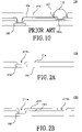
- FIG. 1A to FIG. 1G which illustrate magnified cross-sectional views of the bump of a wafer showing the steps for producing a bump according to a conventional method.
- a wafer 100 having an active surface 101 with a plurality of bonding pads 102 (only one is shown) and a passivation layer 104 thereon is provided.
- the passivation layer 104 are positioned over the active surface 101 and exposes the bonding pads 102 through passivation openings 104 a (only one is shown) formed in the passivation layer 104 .
- a first dielectric layer 105 is formed over the passivation layer 104 and covers a portion of each bonding pad 102 to leave one of bonding pads 102 exposed out of the first dielectric layer 105 through a first opening 105 a and have a portion of passivation layer 104 exposed out of the first dielectric layer 105 through a second opening 105 b.
- a redistributed layer 106 is formed over the first dielectric layer 105 , the bonding pad 102 and the passivation layer 104 exposed out of the first dielectric layer 105 , wherein the portion of the redistributed layer 106 directly connecting the passivation layer 104 serves as a bump pad 106 a .
- the redistributed layer 106 is formed by the following steps. Firstly, a first electrically conductive layer is formed over the first dielectric layer. Next, a photo-resist layer is formed on and partially covers the first electrically conductive layer.
- a photolithographic process and an etching process are performed to remove the portion of the first electrically conductive layer not covered by the photo-resist layer to form a patterned first electrically conductive layer serving as the redistributed layer as mentioned above.
- the bump pad is electrically connected to the bonding pad through said patterned first electrically conductive layer.
- a patterned second electrically conductive layer 107 is formed over the redistributed pad 106 a by the steps of disposing photo-resist layer, performing a photolithographic process, and performing an etching process and serves as a transition layer or an under bump metallurgy layer located over the bump pad 106 a.
- a second dielectric layer 108 is formed over the patterned first electrically conductive layer 106 with a third opening 108 a exposing the portion of the patterned second electrically conductive layer 107 , which is located over the bump pad 106 a.
- a photo-resist layer 109 is formed over the second dielectric layer 108 with a fourth opening 109 a exposing the portion of the patterned second electrically conductive layer 107 located over the bump pad 106 a . Then, a solder material is filled in the fourth opening 109 a through a screen-printing method to form a bump 110 .
- the bump 110 is reflowed to be fixed on the patterned second electrically conductive layer 107 over the bump pad 106 a securely and shaped into a solder ball 112 ; and the second dielectric layer 108 is removed in sequence.
- the solder material is a mixture of solder powder and flux
- the second dielectric layer 108 is usually made of a polymer material, such as polyimide (PI) and Benzocyclobutene (BCB).
- PI polyimide
- BCB Benzocyclobutene
- the flux within the solder material will react with the polymer material to produce water and carbon dioxide or some other gases, so the gases including water and carbon dioxide inside the bump 126 will form air bubbles and said bubbles will stay in the reflowed bump, after the reflow process is performed as shown in FIG. 1G .
- the mechanical strength of the bump will be lowered to reduce the reliability of the bump.
- the photo-resist layer 109 is typically removed by etching with an etchant.
- the etchant not only etches away the photo-resist layer 109 , but also attach the second dielectric layer 108 made of polymer material underneath the photo-resist layer 109 so that a portion of the second dielectric layer 108 will be removed or damaged. Any loss of integrity of the polymer layer 108 is likely to compromise the protective capacity on the wafer 100 .
- an objective of this invention is to provide a method of forming bumps capable of reducing bubbles inside the bumps to enhance the reliability of bumps.
- the invention provides a bumping process including the following steps. Firstly, a first dielectric layer is formed over the active surface of the wafer wherein the first dielectric layer comprising a plurality of first openings and second openings to expose the bonding pads and portions of the passivation layer formed on the active surface of the wafer respectively. Next, a patterned first electrically conductive layer is formed over the first dielectric layer, the exposed portions of the passivation layer through the second openings and the bonding pads exposed out of the first openings.
- a second dielectric layer is formed over the first dielectric layer and the patterned first electrically conductive layer with third openings, which expose portions of the patterned first electrically conductive layer disposed in the second openings to be regarded as the bump pads.
- the bump pads are electrically connected to the bonding pads through the patterned first electrically conductive layer.
- a second electrically conductive layer is formed over the second dielectric layer and the bump pads.
- a plurality of bumps are formed on the second electrically conductive layer and located over the bump pads, and a reflow process is then performed to have said bumps transformed into reflowed bumps which are securely attached to the second electrically conductive layer.
- the second electrically conductive layer is patterned through taking the reflowed bumps as masks to etch away the portions of the second electrically conductive layer not covered by the reflowed bumps and form a patterned second electrically conductive layer.
- the second dielectric layer is covered by the second electrically conductive layer.
- the bumps are separated from the second dielectric layer so as to avoid the flux reacting with the second dielectric layer. Accordingly, the reliability of the reflowed bumps will be kept great.
- the photo-resist layer for defining the locations and size of the bumps is disposed over the second electrically conductive layer. Accordingly, the second dielectric layer located below the second electrically conductive layer will not reacted with the etchant when removing said photo-resist layer. In such a manner, the integrity of the second dielectric layer and the capability of protecting wafer will be kept great.
- the photo-resist layer for defining the locations and size of the bumps is removed before the bumps are reflowed. Accordingly, the bumps will not have bubbles therein due to the reaction of the photo-resist layer with the solder material.
- FIGS. 1A to 1G are partially enlarged cross-sectional views showing the conventional progression of steps for forming a bump.
- FIGS. 2A to 2H are partially enlarged cross-sectional views showing the progression of steps for forming a bump according to the preferred embodiment of this invention.
- FIGS. 2A to 2H are partially enlarged cross-sectional views showing the progression of steps for forming a bump according to the preferred embodiment of this invention.
- a silicon wafer 200 having an active surface 201 , a plurality of bonding pads 202 and a passivation layer 204 .
- the passivation layer 204 with passivation openings 204 a covers the active surface 201 of the silicon wafer 200 and exposes the bonding pads 202 through the passivation openings 204 a.
- a first dielectric layer 205 is formed over the passivation layer 204 to form a plurality of first openings 205 a (only one is shown) and second openings 205 b wherein the first openings 205 a expose the bonding pads 202 and the second openings 205 b expose portions of the passivation layer 204 .
- the first dielectric layer 205 can be made of the material selected from one of polyimide, Benzocyclobutene (BCB) and polymer materials.
- a first electrically conductive layer 206 is formed over the first dielectric layer 205 wherein the first electrically conductive layer 206 may comprise an adhesive layer contacting the bonding pads 202 .
- the adhesive layer comprises a titanium layer or a copper layer.
- a first photo-resist layer 207 is formed on the first electrically conductive layer 206 in order to pattern the first electrically conductive layer 206 by removing the portions of the first electrically conductive layer 206 not covered by the first photo-resist layer 207 to form a patterned first electrically conductive layer 208 as shown in FIG. 2D .
- the first electrically conductive layer 206 can be directly formed on the bonding pads and the passivation layers without disposing said first dielectric layer therebetween.
- a second dielectric layer 209 with third openings 209 a is formed over the first dielectric layer 205 and the patterned first electrically conductive layer 208 , wherein the third openings expose portions of the patterned first electrically conductive layer 208 , directly connecting to the passivation layer 204 , to serve as bump pads 208 a.
- a second electrically conductive layer 210 is formed over the second dielectric layer 209 and the bump pads 208 a; and, a photo-resist layer 211 is then formed over the portions of the second electrically conductive layer 210 , including the portions not covering the bump pads 208 a, to form a fourth openings 211 a therein.
- a conductive material such as a solder material and a gold material, is filled in the openings 211 a to form a plurality of solder bumps 212 .
- the solder material is formed by the method of plating and said solder material may be selected from one of lead-free and solder eutectic.
- a plurality of solder balls can be provided and placed in the third openings 211 a.
- the photo-resist layer 211 is removed and a reflowed process is performed to shape the bumps 213 into a ball-like shape or a solder ball 213
- the second electrically conductive layer 210 is then patterned through taking the reflowed bumps 213 as masks to etch away the portions of the second electrically conductive layer 210 not covered by the reflowed bumps 213 to form patterned second electrically conductive layer 214 .
- the patterned first electrically conductive layer 208 may comprise a titanium layer or an aluminum layer; and the patterned second electrically conductive layer 214 may comprises two layers made of a nickel-vanadium layer and a copper layer or may comprise three layers made of a titanium layer, a nickel-vanadium layer and a copper layer.
- the second dielectric layer is covered by the second electrically conductive layer.
- the bumps are separated from the second dielectric layer so as to avoid the flux reacting with the second dielectric layer. Accordingly, the reliability of the reflowed bumps will be kept great.
- the photo-resist layer for defining the locations and size of the bumps is disposed over the second electrically conductive layer so as to avoid the etchant reacting with the second dielectric layer located below the second electrically conductive layer when removing said photo-resist layer. In such a manner, the integrity of the second dielectric layer and the capability of protecting wafer kept will be kept great.
- the photo-resist layer for defining the locations and size of the bumps is removed before the bumps are reflowed. Accordingly, the bumps will not have bubbles therein due to the reaction of the photo-resist layer with the solder material.
Abstract
Description
Claims (20)
Applications Claiming Priority (2)
| Application Number | Priority Date | Filing Date | Title |
|---|---|---|---|
| TW092117893A TWI225280B (en) | 2003-06-30 | 2003-06-30 | Bumping process |
| TW092117893 | 2003-06-30 |
Publications (2)
| Publication Number | Publication Date |
|---|---|
| US20050009317A1 US20050009317A1 (en) | 2005-01-13 |
| US7223683B2 true US7223683B2 (en) | 2007-05-29 |
Family
ID=33563275
Family Applications (1)
| Application Number | Title | Priority Date | Filing Date |
|---|---|---|---|
| US10/876,582 Active 2024-09-15 US7223683B2 (en) | 2003-06-30 | 2004-06-28 | Wafer level bumping process |
Country Status (2)
| Country | Link |
|---|---|
| US (1) | US7223683B2 (en) |
| TW (1) | TWI225280B (en) |
Cited By (5)
| Publication number | Priority date | Publication date | Assignee | Title |
|---|---|---|---|---|
| US20060125095A1 (en) * | 2004-12-09 | 2006-06-15 | Seiko Epson Corporation | Semiconductor device and manufacturing method thereof |
| US20060226542A1 (en) * | 2005-04-11 | 2006-10-12 | Siliconware Precision Industries Co., Ltd. | Semiconductor device and fabrication method thereof |
| US20080308929A1 (en) * | 2007-06-13 | 2008-12-18 | Himax Technologies Limited | Semiconductor device, chip package and method of fabricating the same |
| US20090117688A1 (en) * | 2005-03-29 | 2009-05-07 | Seiji Karashima | Flip chip mounting method and bump forming method |
| TWI392068B (en) * | 2008-11-11 | 2013-04-01 | Unimicron Technology Corp | Package substrate and fabrication method thereof |
Families Citing this family (6)
| Publication number | Priority date | Publication date | Assignee | Title |
|---|---|---|---|---|
| US7160755B2 (en) * | 2005-04-18 | 2007-01-09 | Freescale Semiconductor, Inc. | Method of forming a substrateless semiconductor package |
| US7323780B2 (en) * | 2005-11-10 | 2008-01-29 | International Business Machines Corporation | Electrical interconnection structure formation |
| US20100117231A1 (en) * | 2006-08-30 | 2010-05-13 | Dennis Lang | Reliable wafer-level chip-scale solder bump structure |
| US7781877B2 (en) | 2007-08-07 | 2010-08-24 | Micron Technology, Inc. | Packaged integrated circuit devices with through-body conductive vias, and methods of making same |
| CN104952827A (en) * | 2014-03-26 | 2015-09-30 | 中芯国际集成电路制造(上海)有限公司 | Pad structure and manufacturing method thereof |
| JP2019169639A (en) * | 2018-03-23 | 2019-10-03 | ルネサスエレクトロニクス株式会社 | Semiconductor device and manufacturing method thereof |
Citations (12)
| Publication number | Priority date | Publication date | Assignee | Title |
|---|---|---|---|---|
| US20010020737A1 (en) * | 1999-07-09 | 2001-09-13 | Kwon Yong Hwan | Chip scale package |
| US6350668B1 (en) * | 1999-06-07 | 2002-02-26 | Kishore K. Chakravorty | Low cost chip size package and method of fabricating the same |
| US6400021B1 (en) * | 1999-06-29 | 2002-06-04 | Hyundai Electronics Industries Co., Ltd. | Wafer level package and method for fabricating the same |
| US20020096764A1 (en) * | 2000-10-13 | 2002-07-25 | Min-Lung Huang | Semiconductor device having bump electrode |
| US6455408B1 (en) * | 1999-09-30 | 2002-09-24 | Samsung Electronics Co., Ltd. | Method for manufacturing semiconductor devices having redistribution patterns with a concave pattern in a bump pad area |
| US6541303B2 (en) * | 2001-06-20 | 2003-04-01 | Micron Technology, Inc. | Method for conducting heat in a flip-chip assembly |
| US6642136B1 (en) * | 2001-09-17 | 2003-11-04 | Megic Corporation | Method of making a low fabrication cost, high performance, high reliability chip scale package |
| US6689680B2 (en) * | 2001-07-14 | 2004-02-10 | Motorola, Inc. | Semiconductor device and method of formation |
| US20040266163A1 (en) * | 2003-06-30 | 2004-12-30 | Advanced Semiconductor Engineering, Inc. | Bumping process |
| US20050048695A1 (en) * | 2002-05-21 | 2005-03-03 | Micron Technology, Inc. | Super high density module with integrated wafer level packages |
| US6869870B2 (en) * | 1998-12-21 | 2005-03-22 | Megic Corporation | High performance system-on-chip discrete components using post passivation process |
| US20050236709A1 (en) * | 2002-08-27 | 2005-10-27 | Eng Meow K | Multiple chip semiconductor package and method of fabricating same |
-
2003
- 2003-06-30 TW TW092117893A patent/TWI225280B/en not_active IP Right Cessation
-
2004
- 2004-06-28 US US10/876,582 patent/US7223683B2/en active Active
Patent Citations (18)
| Publication number | Priority date | Publication date | Assignee | Title |
|---|---|---|---|---|
| US6869870B2 (en) * | 1998-12-21 | 2005-03-22 | Megic Corporation | High performance system-on-chip discrete components using post passivation process |
| US20050230783A1 (en) * | 1998-12-21 | 2005-10-20 | Megic Corporation | High performance system-on-chip discrete components using post passivation process |
| US6350668B1 (en) * | 1999-06-07 | 2002-02-26 | Kishore K. Chakravorty | Low cost chip size package and method of fabricating the same |
| US6400021B1 (en) * | 1999-06-29 | 2002-06-04 | Hyundai Electronics Industries Co., Ltd. | Wafer level package and method for fabricating the same |
| US20010020737A1 (en) * | 1999-07-09 | 2001-09-13 | Kwon Yong Hwan | Chip scale package |
| US6455408B1 (en) * | 1999-09-30 | 2002-09-24 | Samsung Electronics Co., Ltd. | Method for manufacturing semiconductor devices having redistribution patterns with a concave pattern in a bump pad area |
| US20020185721A1 (en) * | 1999-09-30 | 2002-12-12 | Chan Seung Hwang | Chip size package having concave pattern in the bump pad area of redistribution patterns and method for manufacturing the same |
| US20020096764A1 (en) * | 2000-10-13 | 2002-07-25 | Min-Lung Huang | Semiconductor device having bump electrode |
| US6541303B2 (en) * | 2001-06-20 | 2003-04-01 | Micron Technology, Inc. | Method for conducting heat in a flip-chip assembly |
| US20040212102A1 (en) * | 2001-06-20 | 2004-10-28 | Salman Akram | Apparatus for conducting heat in a flip-chip assembly |
| US20030162323A1 (en) * | 2001-06-20 | 2003-08-28 | Salman Akram | Method for conducting heat in a flip-chip assembly |
| US6689680B2 (en) * | 2001-07-14 | 2004-02-10 | Motorola, Inc. | Semiconductor device and method of formation |
| US20040094837A1 (en) * | 2001-07-14 | 2004-05-20 | Greer Stuart E. | Semiconductor device and method of formation |
| US6642136B1 (en) * | 2001-09-17 | 2003-11-04 | Megic Corporation | Method of making a low fabrication cost, high performance, high reliability chip scale package |
| US20050189650A1 (en) * | 2001-09-17 | 2005-09-01 | Megic Corporation | Low fabrication cost, high performance, high reliability chip scale package |
| US20050048695A1 (en) * | 2002-05-21 | 2005-03-03 | Micron Technology, Inc. | Super high density module with integrated wafer level packages |
| US20050236709A1 (en) * | 2002-08-27 | 2005-10-27 | Eng Meow K | Multiple chip semiconductor package and method of fabricating same |
| US20040266163A1 (en) * | 2003-06-30 | 2004-12-30 | Advanced Semiconductor Engineering, Inc. | Bumping process |
Cited By (9)
| Publication number | Priority date | Publication date | Assignee | Title |
|---|---|---|---|---|
| US20060125095A1 (en) * | 2004-12-09 | 2006-06-15 | Seiko Epson Corporation | Semiconductor device and manufacturing method thereof |
| US7598612B2 (en) * | 2004-12-09 | 2009-10-06 | Seiko Epson Corporation | Semiconductor device and manufacturing method thereof |
| US20090117688A1 (en) * | 2005-03-29 | 2009-05-07 | Seiji Karashima | Flip chip mounting method and bump forming method |
| US7531387B1 (en) * | 2005-03-29 | 2009-05-12 | Panasonic Corporation | Flip chip mounting method and bump forming method |
| US20060226542A1 (en) * | 2005-04-11 | 2006-10-12 | Siliconware Precision Industries Co., Ltd. | Semiconductor device and fabrication method thereof |
| US7489037B2 (en) * | 2005-04-11 | 2009-02-10 | Siliconware Precision Industries Co., Ltd. | Semiconductor device and fabrication method thereof |
| US20080308929A1 (en) * | 2007-06-13 | 2008-12-18 | Himax Technologies Limited | Semiconductor device, chip package and method of fabricating the same |
| US7858438B2 (en) * | 2007-06-13 | 2010-12-28 | Himax Technologies Limited | Semiconductor device, chip package and method of fabricating the same |
| TWI392068B (en) * | 2008-11-11 | 2013-04-01 | Unimicron Technology Corp | Package substrate and fabrication method thereof |
Also Published As
| Publication number | Publication date |
|---|---|
| TW200501287A (en) | 2005-01-01 |
| US20050009317A1 (en) | 2005-01-13 |
| TWI225280B (en) | 2004-12-11 |
Similar Documents
| Publication | Publication Date | Title |
|---|---|---|
| US7122459B2 (en) | Semiconductor wafer package and manufacturing method thereof | |
| US7064436B2 (en) | Semiconductor device and method of fabricating the same | |
| EP0714123B1 (en) | A semiconductor device, a semiconductor device-mounted apparatus, and a method for replacing the semiconductor device | |
| US8097941B2 (en) | Semiconductor device having projecting electrode formed by electrolytic plating, and manufacturing method thereof | |
| US7271498B2 (en) | Bump electrodes having multiple under ball metallurgy (UBM) layers | |
| US6348399B1 (en) | Method of making chip scale package | |
| US20080261390A1 (en) | Method for forming bumps on under bump metallurgy | |
| JP2001035965A (en) | Semiconductor package, and manufacture thereof | |
| KR101025349B1 (en) | Semiconductor package and fabricating?method?thereof | |
| US7091121B2 (en) | Bumping process | |
| US7223683B2 (en) | Wafer level bumping process | |
| US6649507B1 (en) | Dual layer photoresist method for fabricating a mushroom bumping plating structure | |
| US20050233571A1 (en) | Flip chip package, semiconductor package with bumps and method for manufacturing semiconductor package with bumps | |
| US20090091028A1 (en) | Semiconductor device and method of bump formation | |
| US6939790B2 (en) | Wafer bumping process with solder balls bonded to under bump metallurgy layer formed over active surface by forming flux on solder ball surfaces and reflowing the solder | |
| JP2005026301A (en) | Semiconductor device, its manufacturing method, circuit board, and electronic apparatus | |
| US20040266066A1 (en) | Bump structure of a semiconductor wafer and manufacturing method thereof | |
| US6429046B1 (en) | Flip chip device and method of manufacture | |
| US7112523B2 (en) | Bumping process | |
| US20060160348A1 (en) | Semiconductor element with under bump metallurgy structure and fabrication method thereof | |
| US6956293B2 (en) | Semiconductor device | |
| US7015130B2 (en) | Method for making UBM pads and bumps on wafer | |
| US7144801B2 (en) | Bumping process to increase bump height | |
| US7261828B2 (en) | Bumping process | |
| US20050181538A1 (en) | Semiconductor device for wire-bonding and flip-chip bonding package and manufacturing method thereof |
Legal Events
| Date | Code | Title | Description |
|---|---|---|---|
| AS | Assignment |
Owner name: ADVANCED SEMICONDUCTOR ENGINEERING, INC., TAIWAN Free format text: ASSIGNMENT OF ASSIGNORS INTEREST;ASSIGNOR:LIN, CHIAN-CHI;REEL/FRAME:015523/0245 Effective date: 20040610 |
|
| STCF | Information on status: patent grant |
Free format text: PATENTED CASE |
|
| FPAY | Fee payment |
Year of fee payment: 4 |
|
| FPAY | Fee payment |
Year of fee payment: 8 |
|
| MAFP | Maintenance fee payment |
Free format text: PAYMENT OF MAINTENANCE FEE, 12TH YEAR, LARGE ENTITY (ORIGINAL EVENT CODE: M1553); ENTITY STATUS OF PATENT OWNER: LARGE ENTITY Year of fee payment: 12 |