US7230669B1 - Liquid crystal display and method of fabricating the same - Google Patents
Liquid crystal display and method of fabricating the same Download PDFInfo
- Publication number
- US7230669B1 US7230669B1 US09/577,032 US57703200A US7230669B1 US 7230669 B1 US7230669 B1 US 7230669B1 US 57703200 A US57703200 A US 57703200A US 7230669 B1 US7230669 B1 US 7230669B1
- Authority
- US
- United States
- Prior art keywords
- liquid crystal
- substrate
- sealing material
- light
- frame
- Prior art date
- Legal status (The legal status is an assumption and is not a legal conclusion. Google has not performed a legal analysis and makes no representation as to the accuracy of the status listed.)
- Expired - Fee Related
Links
Images


Classifications
-
- G—PHYSICS
- G02—OPTICS
- G02F—OPTICAL DEVICES OR ARRANGEMENTS FOR THE CONTROL OF LIGHT BY MODIFICATION OF THE OPTICAL PROPERTIES OF THE MEDIA OF THE ELEMENTS INVOLVED THEREIN; NON-LINEAR OPTICS; FREQUENCY-CHANGING OF LIGHT; OPTICAL LOGIC ELEMENTS; OPTICAL ANALOGUE/DIGITAL CONVERTERS
- G02F1/00—Devices or arrangements for the control of the intensity, colour, phase, polarisation or direction of light arriving from an independent light source, e.g. switching, gating or modulating; Non-linear optics
- G02F1/01—Devices or arrangements for the control of the intensity, colour, phase, polarisation or direction of light arriving from an independent light source, e.g. switching, gating or modulating; Non-linear optics for the control of the intensity, phase, polarisation or colour
- G02F1/13—Devices or arrangements for the control of the intensity, colour, phase, polarisation or direction of light arriving from an independent light source, e.g. switching, gating or modulating; Non-linear optics for the control of the intensity, phase, polarisation or colour based on liquid crystals, e.g. single liquid crystal display cells
- G02F1/133—Constructional arrangements; Operation of liquid crystal cells; Circuit arrangements
- G02F1/1333—Constructional arrangements; Manufacturing methods
- G02F1/1339—Gaskets; Spacers; Sealing of cells
-
- G—PHYSICS
- G02—OPTICS
- G02F—OPTICAL DEVICES OR ARRANGEMENTS FOR THE CONTROL OF LIGHT BY MODIFICATION OF THE OPTICAL PROPERTIES OF THE MEDIA OF THE ELEMENTS INVOLVED THEREIN; NON-LINEAR OPTICS; FREQUENCY-CHANGING OF LIGHT; OPTICAL LOGIC ELEMENTS; OPTICAL ANALOGUE/DIGITAL CONVERTERS
- G02F1/00—Devices or arrangements for the control of the intensity, colour, phase, polarisation or direction of light arriving from an independent light source, e.g. switching, gating or modulating; Non-linear optics
- G02F1/01—Devices or arrangements for the control of the intensity, colour, phase, polarisation or direction of light arriving from an independent light source, e.g. switching, gating or modulating; Non-linear optics for the control of the intensity, phase, polarisation or colour
- G02F1/13—Devices or arrangements for the control of the intensity, colour, phase, polarisation or direction of light arriving from an independent light source, e.g. switching, gating or modulating; Non-linear optics for the control of the intensity, phase, polarisation or colour based on liquid crystals, e.g. single liquid crystal display cells
- G02F1/1303—Apparatus specially adapted to the manufacture of LCDs
-
- G—PHYSICS
- G02—OPTICS
- G02F—OPTICAL DEVICES OR ARRANGEMENTS FOR THE CONTROL OF LIGHT BY MODIFICATION OF THE OPTICAL PROPERTIES OF THE MEDIA OF THE ELEMENTS INVOLVED THEREIN; NON-LINEAR OPTICS; FREQUENCY-CHANGING OF LIGHT; OPTICAL LOGIC ELEMENTS; OPTICAL ANALOGUE/DIGITAL CONVERTERS
- G02F1/00—Devices or arrangements for the control of the intensity, colour, phase, polarisation or direction of light arriving from an independent light source, e.g. switching, gating or modulating; Non-linear optics
- G02F1/01—Devices or arrangements for the control of the intensity, colour, phase, polarisation or direction of light arriving from an independent light source, e.g. switching, gating or modulating; Non-linear optics for the control of the intensity, phase, polarisation or colour
- G02F1/13—Devices or arrangements for the control of the intensity, colour, phase, polarisation or direction of light arriving from an independent light source, e.g. switching, gating or modulating; Non-linear optics for the control of the intensity, phase, polarisation or colour based on liquid crystals, e.g. single liquid crystal display cells
- G02F1/133—Constructional arrangements; Operation of liquid crystal cells; Circuit arrangements
- G02F1/1333—Constructional arrangements; Manufacturing methods
- G02F1/1335—Structural association of cells with optical devices, e.g. polarisers or reflectors
- G02F1/133509—Filters, e.g. light shielding masks
-
- G—PHYSICS
- G02—OPTICS
- G02F—OPTICAL DEVICES OR ARRANGEMENTS FOR THE CONTROL OF LIGHT BY MODIFICATION OF THE OPTICAL PROPERTIES OF THE MEDIA OF THE ELEMENTS INVOLVED THEREIN; NON-LINEAR OPTICS; FREQUENCY-CHANGING OF LIGHT; OPTICAL LOGIC ELEMENTS; OPTICAL ANALOGUE/DIGITAL CONVERTERS
- G02F1/00—Devices or arrangements for the control of the intensity, colour, phase, polarisation or direction of light arriving from an independent light source, e.g. switching, gating or modulating; Non-linear optics
- G02F1/01—Devices or arrangements for the control of the intensity, colour, phase, polarisation or direction of light arriving from an independent light source, e.g. switching, gating or modulating; Non-linear optics for the control of the intensity, phase, polarisation or colour
- G02F1/13—Devices or arrangements for the control of the intensity, colour, phase, polarisation or direction of light arriving from an independent light source, e.g. switching, gating or modulating; Non-linear optics for the control of the intensity, phase, polarisation or colour based on liquid crystals, e.g. single liquid crystal display cells
- G02F1/133—Constructional arrangements; Operation of liquid crystal cells; Circuit arrangements
- G02F1/1333—Constructional arrangements; Manufacturing methods
- G02F1/1341—Filling or closing of cells
-
- G—PHYSICS
- G02—OPTICS
- G02F—OPTICAL DEVICES OR ARRANGEMENTS FOR THE CONTROL OF LIGHT BY MODIFICATION OF THE OPTICAL PROPERTIES OF THE MEDIA OF THE ELEMENTS INVOLVED THEREIN; NON-LINEAR OPTICS; FREQUENCY-CHANGING OF LIGHT; OPTICAL LOGIC ELEMENTS; OPTICAL ANALOGUE/DIGITAL CONVERTERS
- G02F1/00—Devices or arrangements for the control of the intensity, colour, phase, polarisation or direction of light arriving from an independent light source, e.g. switching, gating or modulating; Non-linear optics
- G02F1/01—Devices or arrangements for the control of the intensity, colour, phase, polarisation or direction of light arriving from an independent light source, e.g. switching, gating or modulating; Non-linear optics for the control of the intensity, phase, polarisation or colour
- G02F1/13—Devices or arrangements for the control of the intensity, colour, phase, polarisation or direction of light arriving from an independent light source, e.g. switching, gating or modulating; Non-linear optics for the control of the intensity, phase, polarisation or colour based on liquid crystals, e.g. single liquid crystal display cells
- G02F1/133—Constructional arrangements; Operation of liquid crystal cells; Circuit arrangements
- G02F1/1333—Constructional arrangements; Manufacturing methods
- G02F1/133388—Constructional arrangements; Manufacturing methods with constructional differences between the display region and the peripheral region
-
- G—PHYSICS
- G02—OPTICS
- G02F—OPTICAL DEVICES OR ARRANGEMENTS FOR THE CONTROL OF LIGHT BY MODIFICATION OF THE OPTICAL PROPERTIES OF THE MEDIA OF THE ELEMENTS INVOLVED THEREIN; NON-LINEAR OPTICS; FREQUENCY-CHANGING OF LIGHT; OPTICAL LOGIC ELEMENTS; OPTICAL ANALOGUE/DIGITAL CONVERTERS
- G02F1/00—Devices or arrangements for the control of the intensity, colour, phase, polarisation or direction of light arriving from an independent light source, e.g. switching, gating or modulating; Non-linear optics
- G02F1/01—Devices or arrangements for the control of the intensity, colour, phase, polarisation or direction of light arriving from an independent light source, e.g. switching, gating or modulating; Non-linear optics for the control of the intensity, phase, polarisation or colour
- G02F1/13—Devices or arrangements for the control of the intensity, colour, phase, polarisation or direction of light arriving from an independent light source, e.g. switching, gating or modulating; Non-linear optics for the control of the intensity, phase, polarisation or colour based on liquid crystals, e.g. single liquid crystal display cells
- G02F1/133—Constructional arrangements; Operation of liquid crystal cells; Circuit arrangements
- G02F1/1333—Constructional arrangements; Manufacturing methods
- G02F1/1335—Structural association of cells with optical devices, e.g. polarisers or reflectors
- G02F1/133509—Filters, e.g. light shielding masks
- G02F1/133512—Light shielding layers, e.g. black matrix
-
- G—PHYSICS
- G02—OPTICS
- G02F—OPTICAL DEVICES OR ARRANGEMENTS FOR THE CONTROL OF LIGHT BY MODIFICATION OF THE OPTICAL PROPERTIES OF THE MEDIA OF THE ELEMENTS INVOLVED THEREIN; NON-LINEAR OPTICS; FREQUENCY-CHANGING OF LIGHT; OPTICAL LOGIC ELEMENTS; OPTICAL ANALOGUE/DIGITAL CONVERTERS
- G02F1/00—Devices or arrangements for the control of the intensity, colour, phase, polarisation or direction of light arriving from an independent light source, e.g. switching, gating or modulating; Non-linear optics
- G02F1/01—Devices or arrangements for the control of the intensity, colour, phase, polarisation or direction of light arriving from an independent light source, e.g. switching, gating or modulating; Non-linear optics for the control of the intensity, phase, polarisation or colour
- G02F1/13—Devices or arrangements for the control of the intensity, colour, phase, polarisation or direction of light arriving from an independent light source, e.g. switching, gating or modulating; Non-linear optics for the control of the intensity, phase, polarisation or colour based on liquid crystals, e.g. single liquid crystal display cells
- G02F1/133—Constructional arrangements; Operation of liquid crystal cells; Circuit arrangements
- G02F1/1333—Constructional arrangements; Manufacturing methods
- G02F1/1335—Structural association of cells with optical devices, e.g. polarisers or reflectors
- G02F1/133509—Filters, e.g. light shielding masks
- G02F1/133514—Colour filters
- G02F1/133516—Methods for their manufacture, e.g. printing, electro-deposition or photolithography
-
- G—PHYSICS
- G02—OPTICS
- G02F—OPTICAL DEVICES OR ARRANGEMENTS FOR THE CONTROL OF LIGHT BY MODIFICATION OF THE OPTICAL PROPERTIES OF THE MEDIA OF THE ELEMENTS INVOLVED THEREIN; NON-LINEAR OPTICS; FREQUENCY-CHANGING OF LIGHT; OPTICAL LOGIC ELEMENTS; OPTICAL ANALOGUE/DIGITAL CONVERTERS
- G02F1/00—Devices or arrangements for the control of the intensity, colour, phase, polarisation or direction of light arriving from an independent light source, e.g. switching, gating or modulating; Non-linear optics
- G02F1/01—Devices or arrangements for the control of the intensity, colour, phase, polarisation or direction of light arriving from an independent light source, e.g. switching, gating or modulating; Non-linear optics for the control of the intensity, phase, polarisation or colour
- G02F1/13—Devices or arrangements for the control of the intensity, colour, phase, polarisation or direction of light arriving from an independent light source, e.g. switching, gating or modulating; Non-linear optics for the control of the intensity, phase, polarisation or colour based on liquid crystals, e.g. single liquid crystal display cells
- G02F1/133—Constructional arrangements; Operation of liquid crystal cells; Circuit arrangements
- G02F1/1333—Constructional arrangements; Manufacturing methods
- G02F1/1335—Structural association of cells with optical devices, e.g. polarisers or reflectors
- G02F1/13356—Structural association of cells with optical devices, e.g. polarisers or reflectors characterised by the placement of the optical elements
- G02F1/133565—Structural association of cells with optical devices, e.g. polarisers or reflectors characterised by the placement of the optical elements inside the LC elements, i.e. between the cell substrates
-
- G—PHYSICS
- G02—OPTICS
- G02F—OPTICAL DEVICES OR ARRANGEMENTS FOR THE CONTROL OF LIGHT BY MODIFICATION OF THE OPTICAL PROPERTIES OF THE MEDIA OF THE ELEMENTS INVOLVED THEREIN; NON-LINEAR OPTICS; FREQUENCY-CHANGING OF LIGHT; OPTICAL LOGIC ELEMENTS; OPTICAL ANALOGUE/DIGITAL CONVERTERS
- G02F1/00—Devices or arrangements for the control of the intensity, colour, phase, polarisation or direction of light arriving from an independent light source, e.g. switching, gating or modulating; Non-linear optics
- G02F1/01—Devices or arrangements for the control of the intensity, colour, phase, polarisation or direction of light arriving from an independent light source, e.g. switching, gating or modulating; Non-linear optics for the control of the intensity, phase, polarisation or colour
- G02F1/13—Devices or arrangements for the control of the intensity, colour, phase, polarisation or direction of light arriving from an independent light source, e.g. switching, gating or modulating; Non-linear optics for the control of the intensity, phase, polarisation or colour based on liquid crystals, e.g. single liquid crystal display cells
- G02F1/133—Constructional arrangements; Operation of liquid crystal cells; Circuit arrangements
- G02F1/1333—Constructional arrangements; Manufacturing methods
- G02F1/1341—Filling or closing of cells
- G02F1/13415—Drop filling process
-
- G—PHYSICS
- G02—OPTICS
- G02F—OPTICAL DEVICES OR ARRANGEMENTS FOR THE CONTROL OF LIGHT BY MODIFICATION OF THE OPTICAL PROPERTIES OF THE MEDIA OF THE ELEMENTS INVOLVED THEREIN; NON-LINEAR OPTICS; FREQUENCY-CHANGING OF LIGHT; OPTICAL LOGIC ELEMENTS; OPTICAL ANALOGUE/DIGITAL CONVERTERS
- G02F2202/00—Materials and properties
- G02F2202/02—Materials and properties organic material
- G02F2202/022—Materials and properties organic material polymeric
- G02F2202/023—Materials and properties organic material polymeric curable
Definitions
- the present invention relates to a liquid crystal display (LCD) and a fabrication method thereof. Particularly, the present invention relates to the liquid crystal display in which liquid crystal is sealed between two panels by using an instilling method and the fabrication thereof.
- LCD liquid crystal display
- FIG. 104 shows a part of an upper surface of an active matrix-type liquid crystal display panel using a TFT (thin film transistor) as a switching element viewed from a color filter substrate side.
- TFT thin film transistor
- FIG. 104 on a liquid crystal display panel 1100 , a plurality of pixel areas 1114 arranged in a matrix shape are formed on an array substrate 1116 side, and a TFT 1112 is formed in each pixel area 1114 .
- a display area 1110 is structured by the plurality of the pixel areas 1114 .
- a gate electrode of a TFT 1112 in each pixel area 1114 is connected to a gate wiring and a drain electrode is connected to a data wiring respectively. Further, a source electrode of the TFT 1112 is connected to a pixel electrode formed in the pixel area 1114 .
- a plurality of the data wirings and the gate wirings are connected to a terminal portion 1102 formed in the external periphery of the array substrate 1116 so that the plurality of the data wirings and the gate wirings are connected to a driving circuit (not shown in the diagram) provided externally.
- a common electrode (not shown in the diagram) is formed and at the same time, BM (black matrix: shading film) 1080 , 1180 and the like using color filters (shown by letters R(red), G(green) and B(blue) in the diagram), a Cr (chrome) film or the like are formed. Since a BM 1118 demarcates the plurality of the pixel area 1114 in the display area 1110 and earns contrast, the BM 1118 is used for preventing a light leakage from occurring by shading the TFT 1112 . Further, a BM picture-frame portion 1108 is provided for shading undesired light from outside the display area 1110 .
- the array substrate 1116 and the CF substrate 1104 are attached by a sealing material 1106 made of photo-curing type resin.
- a fabrication process of the liquid crystal display is roughly classified into an array process in which a wiring pattern, a switching element (in a case of active matrix type) and the like are formed, a cell process in which an alignment layer treatment is performed, spacers are arranged and liquid crystal is sealed between opposing glass substrates, and a module process in which an installation of a driver IC, attachment of a back light and the like are performed.
- a method vacuum injection method
- the array substrate 1116 forming the TFT 1112 and the opposite color filter substrate (opposite substrate) 1104 are attached with a use of the sealing material 1106 , the sealing material is cured, then liquid crystal and the substrates are placed in a vacuum chamber, an injection opening opened in the sealing material is immersed in liquid crystal, the inside of the chamber is returned to the atmospheric pressure, thereby sealing the liquid crystal between the substrates.
- an instilling method is drawing attention, in which, for example, a constant amount of liquid crystal is dropped on the substrate surface inside the frame of the sealing material 1106 formed inside a frame shape in the periphery of the array substrate, the array substrate 1116 and the CF substrate 1104 are attached in a vacuum and sealing of liquid crystal is performed.
- FIGS. 108 a through 108 c A fabrication process of the liquid crystal display panel according to the instilling method is briefly described with reference to FIGS. 108 a through 108 c .
- liquid crystal 1206 is dropped from a liquid crystal instilling equipment which is not shown in the diagram at a plurality of positions on an array substrate 1204 forming switching elements such as TFT and the like.
- a common electrode and a color filter are formed in a display area, and an opposite substrate 1200 coated with a UV sealing material 1202 to be cured by ultraviolet (UV) irradiation in the external periphery of a display area is aligned and attached to the array substrate 1204 . This process is performed in a vacuum.
- UV ultraviolet
- this instilling method has possibilities to reduce costs of fabricating a panel and to improve mass productivity owing to first, substantial reduction in the amount of liquid crystal to be used and second, reduction in time to inject liquid crystal and the like, therefore application of this instilling method is strongly desired in the panel fabrication process.
- a method is recorded in which an accurately measured required amount of liquid crystal is mounted on a substrate surface inside a sealing material provided on one substrate, the opposite other substrate is overlaid so that the substrate contacts with an upper surface of the sealing material before the liquid crystal spreads on the first substrate surface and reaches an end face of the peripheral sealing material, then both substrates are pressed in a decompressed environment, and the sealing material is cured.
- the width of a picture-frame portion in the periphery of a panel is becoming narrow due to recent enlargement of the liquid crystal panel 1100 and the like. Therefore, the sealing material 1106 formed in a frame shape in the periphery of a substrate is formed in many cases in the very close proximity to the end of an external periphery of the BM picture-frame portion shown in FIG. 104 . Accordingly, when the array substrate 1116 and the CF substrate 1104 are pressed and the area (hatched area in FIG.
- the area of the sealing material 1106 where the BM picture-frame portion 1108 contacts is shaded and not irradiated by light resulting in generating a curing defect area in the said area.
- FIGS. 105 a and 105 b show liquid crystal instillations in the cell process of a liquid crystal panel in the past.
- FIG. 105 a shows a state when liquid crystal (shown by a mark O) 1144 is dropped in equal intervals (in this example, matrix shape of three rows and four columns) in a similar shape to the frame shape of the sealing material 1106 on an upper surface of the array substrate inside the sealing material 1106 .
- Substrate holding in liquid crystal instillation in the conventional process is performed by using vacuum chucks, electrostatic chucks or a mechanical retainer.
- a substrate is mounted on an attracting surface on a parallel surface plate and is fixed by vacuum-absorbing a back surface of a substrate.
- an array substrate is held and an adequate amount of liquid crystal is dropped on an array substrate surface inside the frame shape of a sealing material by a dispenser and the like.
- a CF substrate is positioned in the vacuum environment and entered into a process to be attached with an array substrate.
- FIGS. 106 a and 106 b are diagrams describing substrate attachment by electrostatic chucks.
- FIG. 106 a shows a plan view of an electrostatically attracted glass substrate 700 of the array substrate 1116 in two-piece structure as an example.
- FIG. 106 b shows a cross section cut by a line A-A in FIG. 106 a when the array substrate 1116 and the CF substrate 1104 are to be attached.
- Electrostatic chucks for electrically attracting the glass substrate 700 has four electrodes 740 , 750 , 760 and 770 on a parallel surface plate.
- the electrodes 740 and 750 among the four electrodes 740 through 770 structure positive electrodes and the electrodes 760 and 770 structure negative electrodes.
- One surface of the array substrate 1116 is electrostatically attracted by the positive electrode 740 and the negative electrode 760 and the other surface of the array substrate 1116 is electrostatically attracted by the positive electrode 750 and the negative 770 .
- Space 680 is provided in a boundary between the positive electrode 740 and the negative electrode 760 and in a boundary between the positive electrode 750 and the negative electrode 770 .
- the electrostatic chucks on a glass substrate 720 forming the CF substrate 1104 has a similar structure to the electrostatic chucks attracting the glass substrate 700 .
- the glass substrate By mounting the glass substrate forming a conductive film on the electrostatic chucks in such structure, applying voltage between the electrode and the conductive film and generating the coulomb's force between the glass and the conductive film, the glass substrate can be attracted.
- the conductive film on the glass substrate 700 includes the pixel electrodes, gate wirings, data wirings and the like formed on the array substrate 1116 area. Further, the conductive film on the glass substrate 720 forming the CF substrate area includes the common electrode and the like.
- the positive poles 740 and 750 are contacted to one of the two substantially equally divided areas of the array substrate 1116 , the negative poles 760 and 770 are contacted to the remaining area, a predetermined voltage is applied between the positive and negative poles and the glass substrate 700 is electrostatically attracted.
- a surface corresponding to the positive poles 740 and 750 in the array substrate 1116 area of the glass substrate 700 is charged with negative ( ⁇ ) electricity and a surface corresponding to the negative poles 760 and 770 are charged with positive (+) electricity.
- a boundary between a positive electric charge and a negative electric charge is formed on the conductive film of the array substrate 1116 corresponding to the air gap 680 of the boundary between the positive and negative poles.
- an alignment film is formed on an upper portion of the conductive film of the array substrate 1116 and liquid crystal is dropped on the alignment film by instillation. Therefore, if the array substrate 1116 area is electrostatically attracted according to the above method, impure ion in liquid crystal is selectively attracted on the alignment film at both sides of the boundary dividing the surface of the array substrate 1116 area into substantially two equal parts. Accordingly, the above method has a problem of generating display irregularities in which when a formed liquid crystal panel is displayed, the brightness in the two surfaces sandwiching the said boundary varies.
- a method in which substrates are held by electrostatic chucks of which the substrate holding strength is not affected by the degree of vacuum also has a problem in which a glow discharge occurs in the course of decompressing the atmospheric pressure for attaching substrates and may generate damage to a circuit or a TFT element on a substrate. Also, a phenomenon may occur in which an operation of the electrostatic chucks becomes unstable due to the air remained between the electrostatic chucks and the substrates, and the substrates break off from the electrostatic chucks in the course of the substrate attachment process.
- liquid crystal In order to evenly spread liquid crystal inside both substrates in the instillation process, liquid crystal is required to be dropped at multiple points on a substrate surface by dispenser or the like.
- the amount of liquid crystal to be dropped per one substrate surface is minute, when dropping positions are scattered into multiple points, an extremely small amount of liquid crystal must be accurately dropped.
- the amount of liquid crystal to be dropped varies due to variations in viscosity or volume of liquid crystal affected by changes in the environment such as temperature variations at the time of instillation or variations in quality of a dispenser. As a result, variations in cell gap between both substrates occur.
- FIGS. 107 a to 107 c are cross sections cut vertical to a liquid crystal panel surface and shows an example of variations in cell gap.
- FIG. 107 a shows a state in which a desired cell gap is obtained by an ideal liquid crystal instillation.
- the array substrate 1116 and the CF substrate 1104 are attached by the sealing material 1106 and a predetermined cell gap is secured by beads 1150 as spacers.
- the sealing material 1106 can not be pressed to an intended gap due to excessive liquid crystal resulting in a problem in which display irregularities occur in the peripheral portion of a panel (periphery of picture-frame portion).
- FIG. 107 c a phenomenon in which a center portion of a panel is expanded due to the sealing material 1106 causing a press defect occurs resulting in display irregularities on a whole surface.
- FIG. 109 shows a partial cross section of the end portion of a liquid crystal display panel.
- An array substrate 1200 and an opposite substrate 1204 face each other through the aid of a sealing material 1202 .
- a pixel electrode and a bus line (in FIG. 109 , these are collectively referred by a code 1212 ) are formed on the array substrate 1200 surface facing the opposite substrate 1204 , an alignment film 1214 is formed on the surface 1212 , a common electrode and a color filter (in FIG.
- a code 1216 is formed on the opposite substrate 1204 surface facing the array substrate 1200 , and an alignment film 1218 is formed on the surface 1216 .
- a predetermined cell gap is kept and the liquid crystal 1206 is sealed between the opposing electrodes. As shown in the diagram, the liquid crystal 1206 at the end portion of a panel contacts with the sealing material 1202 .
- UV irradiation is performed toward the sealing material 1202 for curing the sealing material in such a structure, UV light is slightly dispersed and a liquid crystal 1220 in a hatched area shown in the diagram adjacent to the sealing material 1202 is also irradiated.
- a liquid crystal material is irradiated by UV light, characteristics of liquid crystal are degraded, and specifically, resistivity tends to be reduced and high voltage retention ratio required in TFT-LCD and the like can not be kept. Therefore, operating voltage of a liquid crystal cell is different in comparison with a portion which is not irradiated by UV, display irregularities at half-tone display become prominent.
- photo-curing resin or heat-curing resin is used for a sealing material in the instilling method.
- a technique in which ultraviolet light is irradiated through a mask having a predetermined pattern transmitting light to attached substrates Japanese Laid-open Patent Application No. 09-61829
- a technique in which an upper and lower substrates are arranged facing each other so that a shaded portion is not overlapped with a position a seal is arranged (Japanese Laid-open Patent Application No.
- photo-degradation of liquid crystal can be cited.
- ultraviolet-light-curing resin is used for photo-curing resin because of the preservation ability and the adhesive strength as previously described, when ultraviolet light is irradiated to liquid crystal, photolysis reaction makes progress and an ion impurity is generated.
- This ion impurity causes display defects such as irregularities due to a reduction in voltage retention ratio or in image persistence.
- a use of a mask having a predetermined pattern transmitting light as disclosed in the above document Japanese Laid-open Patent Application No. 09-61829
- this method of using a mask has a problem in which since a mask is required for each seal pattern and the number of processes is increased by a mask alignment process, the goal of the instilling method of liquid crystal such as reducing a fabrication cost of a panel and improving mass productivity may be rather prevented than accomplished.
- enlargement of an outside dimension of a panel can be cited.
- a terminal made of many metal films is formed in a non-display area on the array substrate side.
- a sealing material is arranged as described in the above document (Japanese Laid-open Patent Application No. 09-90383), essentially, a seal is required to be formed outside the picture frame of a black matrix, thereby resulting in enlargement of an outside dimension of a panel.
- a liquid crystal display in which a column-shape spacer is arranged outside the pixel area on either one of a pair of substrates and a frame-shape spacer (frame-shape structure) is arranged along the fringe periphery of the said substrate is disclosed.
- These spacers are simultaneously formed in a photolithography process and are used to fabricate a liquid crystal panel using an instilling method.
- FIG. 110 a shows a part of an upper surface of a conventional active-matrix type liquid crystal panel 1100 different from the one using a TFT as a switching element shown in FIG. 104 viewed from a CF (color filter) substrate side.
- FIG. 110 b shows a partial cross section cut at a line A-A of FIG. 110 a .
- a plurality of pixel areas 1114 arranged in a matrix shape are formed on an array substrate 1116 side of the liquid crystal display panel 1100 and a TFT (not shown in the diagram) is formed in each pixel area 1114 .
- a picture display area 1110 is formed by a plurality of pixel areas 1114 .
- a CF substrate 1104 is formed smaller than the array substrate 1116 by approximately the width of a terminal portion 1102 and arranged facing the array substrate 1116 while sealing a liquid crystal at a predetermined cell gap.
- the array substrate 1116 and the CF substrate 1104 are attached by a main seal 1106 made of photo-curing type resin.
- a width 1106 ′ shown by double dotted lines indicates the width of the main seal 1106 at the time of coating.
- a frame-shape structure 1111 separating the main seal 1106 and the liquid crystal 22 is formed in the area between the main seal 1106 and the display area 1110 .
- the liquid crystal 22 is sealed in the area surrounded by the frame-shape structure 1111 between the array substrate 1116 and the CF substrate 1104 .
- a common electrode (not shown in the diagram) and color filters (indicated by letters R(red), G(green), B(blue) in the diagram) are provided on the CF substrate 1104 .
- a BM picture frame 1108 and a BM deciding the space between pixel areas are also formed on the CF substrate 1104 .
- An external peripheral end of the frame-shape structure 1111 is arranged inside an external peripheral end of the BM picture frame viewed from a direction vertical to the surface of the substrate 1116 . Therefore, a peripheral end portion inside the main seal 1106 overlaps with a peripheral end portion outside the BM picture frame 1108 and an area 1107 is formed.
- UV light is shaded by the BM picture frame 1108 and a curing defect of the main seal 1106 is generated in the area 1107 .
- FIG. 111 if the frame-shape spacer 1111 equivalent to a cell gap alone is provided in the fringe periphery of the CF substrate 1104 when liquid crystal more than the amount to fill the frame-shape spacer 1111 at instillation is dropped, excess liquid crystal flows over the frame-shape spacer 1111 , uncured sealing material 1106 and the liquid crystal 22 make contact, thereby dispersing contaminant. Furthermore, as shown in FIG. 112 , if a cell gap is thick, the liquid crystal 22 easily flows over the frame-shape spacer 1111 before the liquid crystal 22 is completely spread. FIG. 112 shows a state in which a surface of the array substrate 1116 is viewed from the CF substrate 1104 side.
- a boundary 1123 of the liquid crystal 22 at the time of attachment is gradually spread. Before the liquid crystal 22 is completely spread, an uninjected portion of liquid crystal 1121 is formed, and even if there is no excess liquid crystal, since the cell gap is higher than the height of the frame-shape spacer 1111 , the liquid crystal boundary 1123 flows over the frame-shape spacer 1111 and, for example, at a position 1122 , contacts with uncured main seal 1106 . Also, as shown in FIG.
- a black matrix (BM: shading film) is usually formed in the fringe periphery portion (picture frame) of a liquid crystal display substrate.
- BM shading film
- a frame-shape spacer is strategically arranged, when a sealing material is spread after substrates are attached, a part of the sealing material overlaps with the end of a BM picture frame and UV light is obstructed, thereby resulting in curing defects. Since adhesive strength is weak in the portion of a curing defect, external stress is concentrated and peeling of a sealing material is induced. If a position of a sealing material is sufficiently apart from the end of a BM picture frame, such defects do not occur. However, by so doing, the picture-frame area is enlarged and the glass substrate surface can not be efficiently utilized.
- a column-shape spacer equivalent to a cell gap alone is provided in a fringe periphery of a substrate, when liquid crystal more than the amount to fill the frame-shape spacer is dropped at the time of instillation, an excess liquid crystal flows over the frame-shape spacer, uncured sealing material and liquid crystal contact, thereby dispersing contaminant. Further, when there are variations in a dropping amount from a dropping dispenser even if the dropping of liquid crystal is controlled, or when liquid crystal reaches the frame-shape spacer before liquid crystal fully fills inside the frame, since a cell gap is thick before liquid crystal is completely spread, liquid crystal easily flows over the frame-shape spacer.
- FIGS. 114 a through 114 c show an example of the “dropping mark”.
- FIG. 114 c shows a liquid crystal instillation in a state in which a dropped liquid crystal 136 is adhered on an alignment film 134 on a substrate 132 .
- display irregularities due to “dropping marks” there are irregularities 130 as shown in FIG. 114 a in which boundaries of the dropped areas are visible and surface irregularities 131 as shown in FIG. 114 b in which the brightness of the whole dropped areas is different from the brightness of the periphery.
- an instilled panel is positioned and attached, and then liquid crystal is spread in a vacuum.
- the cause of the “dropping mark” is considered to be a contact between liquid crystal and an alignment film in the atmospheric pressure. Further, a degree of the “dropping mark” is found to be different depending on a liquid crystal material for dropping and a material for an alignment film. If a liquid crystal material has strong polarity and a material for liquid crystal and a material used for an alignment film material are inferior in electrical characteristics (i.e. low voltage retention ratio, high ion density, large residual DC voltage), the “dropping mark” tends to be more visibly generated.
- N-type liquid crystal material and a vertical alignment film are required, material selection for these materials is limited in comparison with P-type liquid crystal material and a horizontal alignment film, and there are only few materials among the existing materials which satisfy requirements of electrical characteristics. Therefore, liquid crystal even more reliable is required to be used for a liquid crystal material which contacts with an alignment film in the atmospheric pressure and a different fabrication method from before is required.
- an instilling method has a problem in which administration to prevent substrates failed at instillation due to troubles in the process and substrates failed to create a cell gap adjacent to a main seal from advancing to subsequent processes is difficult.
- a liquid crystal layer is seen as the same as an air layer and grasping a state of liquid crystal instillation with certainty is difficult. Therefore, easily and steadily performing an inspection of display irregularities of a liquid crystal panel fabricated according to an instilling method is desired.
- a use of a sealing material of high viscosity can be considered.
- a gap is difficult to create by a sealing material of high viscosity and a cell gap at the edge of a seal becomes thicker then a cell gap at the center of a display, thereby resulting in generating a problem of display irregularities.
- An object of the present invention is to provide a liquid crystal display and a fabrication method thereof wherein liquid distillation can surely be performed in a cell process.
- a liquid crystal display which comprises a sealing material made of a photo-curing type material sealing liquid crystal sandwiched between two substrates, a shading area overlaying a red-colored layer to transmit color light, a green-colored layer to transmit green light and blue-colored layer transmitting blue light, wherein only the blue-colored layer is formed in the shading area contacting with the sealing material and the photo-curing type material for the sealing material has a light reactive area for a wavelength of blue-color band.
- FIGS. 1 a and 1 b are diagrams showing a schematic structure of a liquid crystal display panel according to a first embodiment of the present invention.
- FIG. 2 is a diagram showing a light transmission spectrum of a red-colored layer 28 , green-colored layer 26 and blue-colored layer 24 when a film thickness is equal to 1.3 nm.
- FIG. 3 is a diagram showing a photo-absorption spectrum ( ⁇ ) of a photo-curing-type resin of a sealing material 6 according to the first embodiment of the present invention and a blue-color transmission spectrum ( ⁇ ) of the blue-colored layer 24 and further showing a photo-absorption spectrum ( ⁇ ) of a conventional photo-curing-type resin for comparison.
- FIGS. 4 a and 4 b are diagrams describing an overlap of the sealing material of a liquid crystal display according to a second embodiment of the present invention and a BM picture-frame portion.
- FIGS. 5 a and 5 b are diagrams showing a comparison example with respect to the liquid crystal display shown in FIGS. 4 a and 4 b in the second embodiment of the present invention.
- FIG. 6 is a diagram describing a relation between the sealing material for corner portions of a liquid crystal display according to the second embodiment of the present invention and a BM picture-frame portion.
- FIG. 7 is a diagram showing a comparison example with respect to the liquid crystal display shown in FIG. 6 in the second embodiment of the present invention.
- FIGS. 8 a and 8 b are diagrams describing a relation between a transfer of a liquid crystal display according to a third embodiment of the present invention and a BM picture-frame portion.
- FIG. 9 is a diagram showing a comparison example with respect to the liquid crystal display shown in FIGS. 8 a and 8 b according to the third embodiment of the present invention.
- FIGS. 10 a and 10 b are diagrams describing a schematic structure of a light source for UV irradiation according to a fourth embodiment of the present invention.
- FIG. 11 is a diagram showing a comparison example with respect to the light source for UV irradiation shown in FIGS. 10 a and 10 b in the fourth embodiment of the present invention.
- FIGS. 12 a and 12 b are diagrams showing a schematic structure of a liquid crystal display according to a fifth embodiment of the present invention.
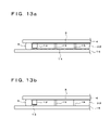
- FIGS. 13 a and 13 b are diagrams showing a schematic structure relative to an example of a variation of the liquid crystal display according to the fifth embodiment of the present invention.
- FIGS. 14 a and 14 b are diagrams showing a schematic structure relative to an example of an other variation of the liquid crystal display according to the fifth embodiment of the present invention.
- FIG. 15 is a diagram showing a UV spectrum of Comparison Example E and Example G in the liquid crystal display according to the fifth embodiment of the present invention.
- FIG. 16 is a diagram describing a creation of a gap adjacent to a frame-shape structure 12 by pressuring the frame-shape structure 12 by a pressure P before a liquid crystal boundary 23 of a liquid crystal 22 reaches the frame-shape structure 12 in the liquid crystal display according to the fifth embodiment of the present invention.
- FIG. 17 is a diagram showing Example 1 in a liquid crystal display and a fabrication method thereof according to a sixth embodiment of the present invention.
- FIGS. 18 a and 18 b are diagrams showing Example 2 in the liquid crystal display and the fabrication method of the liquid crystal display according to the sixth embodiment of the present invention.
- FIG. 19 is a diagram showing Example 3 in the liquid crystal display and the fabrication method of the liquid crystal display according to the sixth embodiment of the present invention.
- FIGS. 20 a and 20 b are diagrams showing Example 4 in the liquid crystal display and the fabrication method of the liquid crystal display according to the sixth embodiment of the present invention.
- FIGS. 21 a and 21 b are diagrams showing Example 5 in the liquid crystal display and the fabrication method of the liquid crystal display according to the sixth embodiment of the present invention.
- FIGS. 22 a and 22 b are diagrams showing Example 6 in the liquid crystal display and the fabrication method of the liquid crystal display according to the sixth embodiment of the present invention.
- FIG. 23 is a diagram showing Example 7 in the liquid crystal display and the fabrication method of the liquid crystal display according to the sixth embodiment of the present invention.
- FIG. 24 is a diagram showing Example 8 in the liquid crystal display and the fabrication method of the liquid crystal display according to the sixth embodiment of the present invention.
- FIGS. 25 a and 25 b are diagrams describing a problem in the past in a seventh embodiment of the present invention.
- FIG. 26 is a diagram describing other problem in the past in the seventh embodiment of the present invention.
- FIGS. 27 a through 27 c are diagrams showing Example 1 in a liquid crystal display and a fabrication method thereof according to the seventh embodiment of the present invention.
- FIG. 28 is a diagram showing Example 2 in the liquid crystal display and the fabrication method of the liquid crystal display according to the seventh embodiment of the present invention.
- FIGS. 29 a and 29 b are diagrams showing Example 3 in the liquid crystal display and the fabrication method of the liquid crystal display according to the seventh embodiment of the present invention.
- FIGS. 30 a and 30 b are diagrams showing Example 4 in the liquid crystal display and the fabrication method of the liquid crystal display according to the seventh embodiment of the present invention.
- FIGS. 31 a through 31 c are diagrams showing Example 5 in the liquid crystal display and the fabrication method of the liquid crystal display according to the seventh embodiment of the present invention.
- FIGS. 32 a and 32 b are diagrams showing a schematic structure of a liquid crystal display according to an eighth embodiment of the present invention.
- FIGS. 33 a through 33 c are diagrams showing a structure of a light reflection layer provided in the liquid crystal display according to the eighth embodiment of the present invention.
- FIG. 34 is a diagram showing a structure of a light reflection layer provided in a reflection-type liquid crystal display as an example of a variation of the eighth embodiment of the present invention.
- FIG. 35 is a diagram describing an example of an irradiation method of UV light according to the eighth embodiment of the present invention.
- FIG. 36 is a diagram showing a partial horizontal cross section of an end portion of a liquid crystal display according to a ninth embodiment of the present invention.
- FIG. 37 is a diagram showing characteristics of two kinds of liquid crystal materials (A) and (B).
- FIGS. 38 a through 38 c are diagrams describing a direction of a polarizing axis 46 in irradiation of a polarized UV according to the ninth embodiment of the present invention.
- FIGS. 39 a and 39 b are diagrams describing the direction of the polarizing axis 46 in irradiation of the polarized UV according to the ninth embodiment of the present invention.
- FIG. 40 is a diagram of a partial horizontal cross section of an end portion of a liquid crystal display according to a tenth embodiment of the present invention and showing a state in which a liquid crystal 22 of negative dielectric anisotropy is instilled and vertically aligned by a vertical alignment film.
- FIGS. 41 a through 41 c are diagrams of a partial horizontal cross section of the end portion of a liquid crystal display according to the tenth embodiment of the present invention and showing a state in which a liquid crystal 22 of positive dielectric anisotropy is instilled and vertically aligned by the vertical alignment film.
- FIGS. 42 a and 42 b are diagrams of a partial horizontal cross section of the end portion of the liquid crystal display according to the tenth embodiment of the present invention and showing a state in which the liquid crystal 22 of positive dielectric anisotropy is instilled and vertically aligned by applying voltage to the liquid crystal 22 .
- FIGS. 43 a and 43 b are diagrams describing Example 4 in a liquid crystal display according to an eleventh embodiment of the present invention.
- FIG. 44 is a diagram describing Example 4 in the liquid crystal display according to the eleventh embodiment of the present invention.
- FIG. 45 is a diagram describing Example 4 in the liquid crystal display according to the eleventh embodiment of the present invention.
- FIG. 46 is a diagram describing Example 4 in the liquid crystal display according to the eleventh embodiment of the present invention.
- FIGS. 47 a and 47 b are diagrams describing Example 5 in the liquid crystal display according to the eleventh embodiment of the present invention.
- FIG. 48 is a diagram describing Example 5 in the liquid crystal display according to the eleventh embodiment of the present invention.
- FIG. 49 is a diagram describing Example 6 in the liquid crystal display according to the eleventh embodiment of the present invention.
- FIG. 50 is a diagram describing Example 7 in the liquid crystal display according to the eleventh embodiment of the present invention.
- FIG. 51 is a diagram describing an example 8 in the liquid crystal display according to the eleventh embodiment of the present invention.
- FIG. 52 is a diagram describing Example 8 in the liquid crystal display according to the eleventh embodiment of the present invention.
- FIG. 53 is a diagram describing Example 8 in the liquid crystal display according to the eleventh embodiment of the present invention.
- FIG. 54 is a diagram describing Example 9 in the liquid crystal display according to the eleventh embodiment of the present invention.
- FIG. 55 is a diagram describing Example 10 in the liquid crystal display according to the eleventh embodiment of the present invention.
- FIGS. 56 a and 56 b are diagrams showing an instillation of liquid crystal in a cell process of a liquid crystal panel according to a twelfth embodiment of the present invention.
- FIG. 57 is a diagram briefly describing an instillation in a fabrication method of a liquid crystal display according to a thirteenth embodiment of the present invention.
- FIG. 58 is a diagram briefly describing the instillation in the fabrication method of the liquid crystal display according to the thirteenth embodiment of the present invention.
- FIG. 59 is a diagram briefly describing the instillation in the fabrication method of the liquid crystal display according to the thirteenth embodiment of the present invention.
- FIG. 60 is a diagram showing an upper surface of a substrate 30 where liquid crystal is dropped in the fabrication method of the liquid crystal display according to the thirteenth embodiment of the present invention.
- FIG. 61 is a diagram describing a dispersion state of dropped liquid crystal in a fourteenth embodiment of the present invention.
- FIG. 62 is a diagram showing a pixel formed in a liquid crystal display panel and a dispersion state of the liquid crystal which is dropped in the pixel formed in the liquid crystal display panel in the fourteenth embodiment of the present invention.
- FIG. 63 is a diagram showing a state in which an outline shape of a front end portion of dispersing liquid crystal is controlled to be substantially a similar shape to a shape of a main seal 6 in the liquid crystal display according to the fourteenth embodiment of the present invention.
- FIG. 64 is a diagram showing a structure 29 for determining a cell gap in the liquid crystal display according to the fourteenth embodiment of the present invention.
- FIG. 65 is a diagram showing structures 28 a and 28 b for controlling liquid crystal dispersion in the liquid crystal display according to the fourteenth embodiment of the present invention.
- FIG. 66 is a diagram showing an example of arrangement of the structures 28 a , 28 b and 29 in the liquid crystal display according to the fourteenth embodiment of the present invention.
- FIGS. 67 a through 67 d are diagrams describing liquid crystal instillation, a substrate attaching process and a substrate holding operation in the substrate attaching process in a liquid crystal display according to a fifteenth embodiment of the present invention.
- FIGS. 68 a and 68 b are diagrams describing substrate attachment with a use of electrostatic chucks in a liquid crystal display according to a sixteenth embodiment of the present invention.
- FIGS. 69 a and 69 b are diagrams describing substrate attachment with a use of electrostatic chucks in a liquid crystal display according to a seventeenth embodiment of the present invention.
- FIGS. 70 a and 70 b are diagrams showing a comparison between a photo-curing process in an instillation according to an eighteenth embodiment of the present invention and a photo-curing process in a conventional instillation.
- FIG. 71 is a diagram showing a schematic structure of a substrate attachment equipment according to the eighteenth embodiment of the present invention.
- FIG. 72 is a diagram briefly describing a fabrication method of a liquid crystal display according to a nineteenth embodiment of the present invention.
- FIG. 73 is a diagram briefly describing the fabrication method of the liquid crystal display according to the nineteenth embodiment of the present invention.
- FIG. 74 is a diagram briefly describing the fabrication method of the liquid crystal display according to the nineteenth embodiment of the present invention.
- FIG. 75 is a diagram briefly describing the fabrication method of the liquid crystal display according to the nineteenth embodiment of the present invention.
- FIG. 76 is a diagram briefly describing the fabrication method of the liquid crystal display according to the nineteenth embodiment of the present invention.
- FIGS. 77 a and 77 b are diagrams briefly describing the fabrication method of the liquid crystal display according to the nineteenth embodiment of the present invention.
- FIG. 78 is a diagram briefly describing the fabrication method of the liquid crystal display according to the nineteenth embodiment of the present invention.
- FIG. 79 is a diagram showing a fabrication method of a liquid crystal display according to a twentieth embodiment of the present invention.
- FIG. 80 is a diagram showing the fabrication method of the liquid crystal display according to the twentieth embodiment of the present invention.
- FIG. 81 is a diagram showing the fabrication method of the liquid crystal display according to the twentieth embodiment of the present invention.
- FIGS. 82 a and 82 b are diagrams showing the fabrication method of the liquid crystal display according to the twentieth embodiment of the present invention.
- FIG. 83 is a diagram showing the fabrication method of the liquid crystal display according to the twentieth embodiment of the present invention.
- FIG. 84 is a diagram showing the fabrication method of the liquid crystal display according to the twentieth embodiment of the present invention.
- FIG. 85 is a diagram showing the fabrication method of the liquid crystal display according to the twentieth embodiment of the present invention.
- FIG. 86 is a diagram showing the fabrication method of the liquid crystal display according to the twentieth embodiment of the present invention.
- FIG. 87 is a diagram showing the fabrication method of the liquid crystal display according to the twentieth embodiment of the present invention.
- FIGS. 88 a and 88 b are diagrams describing substrate attachment in a liquid crystal display according to a twenty-first embodiment of the present invention.
- FIG. 89 is a diagram describing substrate attachment in a liquid crystal display according to a twenty-second embodiment of the present invention.
- FIGS. 90 a through 90 c are diagrams describing a liquid crystal display and a fabrication method thereof according to a twenty-third embodiment of the present invention.
- FIG. 91 is a diagram showing a schematic structure of a substrate of a liquid crystal display according to a twenty-fourth embodiment of the present invention.
- FIG. 92 is a diagram describing protruding portions 96 and 98 of the liquid crystal display according to the twenty-fourth embodiment of the present invention.
- FIG. 93 is a diagram describing an example of a variation of the protruding portions 96 and 98 of the liquid crystal display according to the twenty-fourth embodiment of the present invention.
- FIG. 94 is a diagram showing a liquid crystal instilling equipment used to fabricate the liquid crystal display according to the twenty-fourth embodiment of the present invention.
- FIG. 95 is a diagram showing the results of Example 1 in a fabrication method of a liquid crystal display according to a twenty-fifth embodiment of the present invention and a comparison example.
- FIG. 96 is a diagram showing the result of Example 2 in the fabrication method of the liquid crystal display according to the twenty-fifth embodiment of the present invention.
- FIG. 97 is a diagram showing the result of Example 2 in the fabrication method of the liquid crystal display according to the twenty-fifth embodiment of the present invention.
- FIG. 98 is a diagram showing a pin 90 used in the fabrication method of the liquid crystal display according to the twenty-fifth embodiment of the present invention.
- FIG. 99 is a diagram showing the result of Example 3 in the fabrication method of the liquid crystal display according to the twenty-fifth embodiment of the present invention.
- FIG. 100 is a diagram showing the result of the examples in the fabrication method of the liquid crystal display according to the twenty-fifth embodiment of the present invention.
- FIG. 101 is a diagram showing a schematic structure of an active matrix-type liquid crystal display fabricated by a fabrication method of a liquid crystal display according to a twenty-sixth embodiment of the present invention.
- FIG. 102 is a diagram showing an example of a panel inspection in the fabrication method of the liquid crystal display according to the twenty-sixth embodiment of the present invention.
- FIG. 103 is a diagram showing the example of the panel inspection in the fabrication method of the liquid crystal display according to the twenty-sixth embodiment of the present invention.
- FIG. 104 is a diagram showing a schematic structure of a conventional liquid crystal display panel.
- FIGS. 105 a and 105 b are diagrams showing a liquid crystal instillation in a cell process of the conventional liquid crystal panel.
- FIGS. 106 a and 106 b are diagrams describing substrate attachment by conventional electrostatic chucks.
- FIGS. 107 a to 107 c are diagrams showing irregularities of a cell gap in the conventional liquid crystal panel.
- FIGS. 108 a through 108 c are diagrams describing a fabrication process of a liquid crystal display panel according to an instilling method.
- FIG. 109 is a diagram showing a partial horizontal cross section of an end portion of the conventional liquid crystal display panel.
- FIGS. 110 a and 110 b are diagrams showing a schematic structure of a conventional liquid crystal display.
- FIG. 111 is a diagram describing a problem in a fabrication method of the conventional liquid crystal display.
- FIG. 112 is a diagram describing the problem in the fabrication method of the conventional liquid crystal display.
- FIG. 113 is a diagram describing the problem in the fabrication method of the conventional liquid crystal display.
- FIGS. 114 a , 114 b , and 114 c are diagrams describing the problem in the fabrication method of the conventional liquid crystal display.
- FIG. 1 a shows a part of an upper surface of an active matrix type liquid crystal panel 1 using a TFT as a switching element viewed from a CF substrate side.
- FIG. 1 b shows a partial cross section cut at a line A-A of FIG. 1 a .
- a plurality of pixel areas 14 arranged in a matrix shape are formed on an array substrate 16 side of the liquid crystal panel 1 and a TFT 13 is formed in each of the pixel area 14 . Further, as shown in FIGS. 1 a and 1 b , a picture display area 10 is structured by the plurality of the pixel areas 14 . Although detailed diagrams are omitted, a gate electrode of the TFT 13 of each pixel area 14 is connected to a gate wiring and a drain electrode is connected to a data wiring respectively. Furthermore, a source electrode of the TFT 13 is connected to a pixel electrode formed in the pixel area 14 . A plurality of the data wirings and the gate wirings are connected to a terminal portion 2 formed in an external periphery of the array substrate 16 to be connected to a driving circuit (not shown in the diagram) provided outside.
- the array substrate 16 and the CF substrate 4 are attached by a sealing material 6 made of a photo-curing type resin.
- the photo-curing type resin of the sealing material 6 to be described in detail later has light reactive area for the light with the wavelength of a blue-color band.
- a liquid crystal 22 is sealed in the area surrounded by the sealing material 6 between the array substrate 16 and the CF substrate 4 .
- Color filters (shown by the letters R(red), G (green), B (blue) in the diagram) along with a common electrode (not shown in the diagram) are arranged on the CF substrate 4 .
- BM's 8 and 18 laminating a color filter forming material and having a shading function are formed on the CF substrate 4 .
- the BM 18 is used to earn contrast by deciding the plurality of the pixel areas 14 in the display area 10 and to prevent the light leakage current from generating by shading the TFT 13 .
- a BM picture-frame portion 8 is arranged to shade undesired light from outside the display area 10 .
- the BM Picture-frame portion 8 as shown in FIG.
- FIG. 1 b is formed by laminating (by overlaying color-plates) sequentially from the CF substrate 4 , for example, a blue-colored layer 24 made of resin dispersing blue-color pigment, a green-colored layer 26 made of resin dispersing green-color pigment and a red-colored layer 28 made of resin dispersing red-color pigment.
- FIG. 2 shows the photo-transmission spectrum of the red-colored layer 28 , the green-colored layer 26 and the blue-colored layer 24 when the film thickness is approximately 1.3 nm and the lateral axis indicates the wavelength and the vertical axis indicates the transmissivity. As shown in FIG.
- the peak wavelength of the photo-transmission spectrum for the red-colored layer 28 is equal to 650 ⁇ 10 nm
- the peak wavelength of the photo-transmission spectrum for the green-colored layer 26 is equal to 540 ⁇ 10 nm
- the peak wavelength of the photo-transmission spectrum for the blue-colored layer 24 is equal to 460 ⁇ 10 nm.
- an area 20 in which only the blue-colored layer 24 is formed to make contact with the sealing material 6 and the green-colored layer 26 and the red-colored layer 28 are not formed is arranged in the contacting area of sealing material 6 in the periphery of the BM picture-frame portion 8 .
- this embodiment is the liquid crystal display 1 providing the sealing material 6 made of the photo-curing type material to seal the liquid crystal 22 sandwiched between the two substrates 4 and 16 and shading films 8 and 18 having shading areas overlaying the red-colored layer 28 , the green-colored layer 26 and the blue-colored layer 24 , and has distinctive characteristics that only the blue-colored layer 24 transmitting blue-color light is formed at the shading film 8 area contacting the sealing material 6 and the photo-curing type material for the sealing material 6 is, for example, a resin material having the light reactive area for the light with the wavelength of the blue-color band.
- the red-colored layer 28 , the green-colored layer 26 and the blue-colored layer 24 forming the shading areas of the shading films 8 and 18 have a distinctive characteristic in using the color filter forming material for each color.
- the peak wavelength of the extinction rate for the photo-curing type resin according to this embodiment is shifted to the blue-color transmission spectrum ( ⁇ ) side in comparison with that of the conventional resin. Further, the half-width of the spectrum is wider in comparison with that of the conventional resin and a gentle curve from the peak extends to a relatively wide wavelength band. Accordingly, the photo-absorption spectrum ( ⁇ ) of the photo-curing type resin according to this embodiment and the blue-color transmission spectrum ( ⁇ ) of the blue-colored layer 24 have an overlapping wavelength band as shown by hatching in FIG. 3 .
- the sealing material 6 made of the photo-curing type resin according to this embodiment contacts with the BM picture-frame portion 8 at the area 20 , the light in the blue-color band transmitting the blue-colored layer 24 is irradiated in the curing process by irradiation, and thereby the subject area can sufficiently be cured without generating curing defects.
- the reason for using the blue-colored layer 24 is because the transmission spectrum for blue-color light is most on the short wavelength side as already shown in FIG. 2 and is close to the absorption spectrum for a general photo-curing type resin in the transmission spectrum of each color of the color filters.
- Light reactive area of the photo-curing type resin vary depending on the kind of photo-initiator to be added.
- the photo-initiator having the absorption area on longer wavelength side than the past is added to have the wavelength band overlap with the transmission spectrum of the blue-color resin.
- the frame-shape sealing material 6 is formed on the array substrate 16 to have the relative position shown in FIGS. 1 a and 1 b .
- the CF substrate is attached to the array substrate 16 .
- the blue-colored layer 24 of the BM picture-frame portion 8 and at least a part of the sealing material 6 overlap in the area 20 .
- the sealing material curing is performed at this state by irradiating light 30 from upper portion of the surface of the CF substrate 4 .
- the fabrication method of the liquid crystal display according to this embodiment seals the liquid crystal 22 by attaching the two substrates 4 and 16 using the sealing material 6 made of the photo-curing type material and in the fabrication method of the liquid crystal display fixing the two substrates 4 and 16 by curing the sealing material 6 by irradiating the light 30 , uses the photo-curing type resin having the light reactive area to the light with the wavelength of the blue-color band as the photo-curing type material and forms only the blue-colored layer 24 to transmit the light of the blue-color band in the area 20 of the BM picture-frame portion 8 contacting the sealing material 6 when attaching the two substrates 4 and 16 .
- the blue-colored layer 24 is simultaneously formed when a blue-color color filter to be formed in the pixel is formed.
- the light 32 in the blue-color band can be incident upon the sealing material 6 contacting the area 20 . Therefore, the sealing material 6 using the photo-curing type resin having the light reactive area to the light with the wavelength of the blue-color band can be cured.
- FIG. 4 a shows a state of the liquid crystal display according to this embodiment viewed from the opposite substrate 4 side.
- FIG. 4 b is an enlarged cross sectional view of a circled area 290 of FIG. 4 a .
- a black matrix (BM) picture-frame portion 108 for shading is formed in the periphery of a display area where a color filter (CF) 230 of the opposing substrates is formed.
- This embodiment has a distinctive characteristic in coating the sealing material 6 so that a part of the internal periphery side of the sealing material 6 formed in the external periphery of the display area of the opposite substrate 4 overlaps the BM picture-frame portion 108 .
- the sealing material 6 is cured by vertically irradiating UV light from upper portion of the surface of the opposite substrate 4 .
- the ultraviolet transmissivity of the color plate for the color filter (CF) is described with reference to Table 1.
- the CF shown in Table 1 is a combination of each CF of the three primary colors red (R), green (G) and blue (B).
- R red
- G green
- B blue
- the peaks of the bright line specifically degrading liquid crystal by the UV light which transmits and is incident upon the glass substrate are a line j (313 nm) and a line i (365 nm) as shown in Table 1.
- the color plate for the color filter hardly transmits (transmissivity 1-2%) the line j and the line i, and the BM does not transmit either the line j nor the line i as well.
- the color filter is used as a shading mask against the UV light, damages to the liquid crystal can be suppressed and other shading mask for each pattern to form the sealing material 6 is not required to prepare.
- the end portion of the sealing material 6 overlaps in the BM picture-frame portion 108 , the liquid crystal 22 does not expose between the end portion of the sealing material 6 and the end portion of the BM picture-frame portion 108 and thereby the liquid crystal is not directly irradiated by the ultraviolet and the degradation of the liquid crystal can be prevented. Accordingly, a high-quality picture display without display irregularities can be performed. Furthermore, enlarging an outside dimension of a panel at instillation can be suppressed.
- FIGS. 5 a and 5 b show a comparative example.
- FIG. 5 a shows a state of the conventional liquid crystal display viewed from an opposite substrate 200 side.
- FIG. 5 b is an enlarged cross sectional view of a circled area 292 of FIG. 5 a .
- a space 220 is formed between the internal periphery side of a sealing material 202 formed in the external periphery of the display area of the opposite substrate 200 and the BM picture-frame portion 108 and the liquid crystal inside is in a state to be seen through the glass substrate.
- the sealing material 202 is coated on the opposite substrate 200 so that the width (C) of the sealing material 202 after pressing is equal to approximately 1.0 mm and the distance (D) between the end portion of the sealing material 202 and the end portion of the BM picture-frame portion 108 is equal to 0.5 mm.
- the sealing material 202 is cured by irradiating the UV light vertically from upper part of the substrate surface of the opposite substrate 200 .
- the liquid crystal layer exposes when irradiating the UV in this comparative example, display irregularities due to degradation of liquid crystal occur all around the edge of seal.
- the distance (D) between the end portion of the sealing material 202 and the end portion of the BM picture-frame portion 108 becomes an obstacle to reduce the outside dimension of the panel.
- the distance (B) overlapping the sealing material 6 and the BM picture-frame portion 108 is equal to 0.2 mm
- the end portion of the sealing material 6 is non-photo-curable. Since when the light initiator is irradiated and cloven activated species spread, the sealing material 6 can be cured if an overlapping distance is moderately fair even if there is a shading portion.
- the overlapping distance (B) can be equal to approximately 0.5 mm.
- the UV light having transmitted through the sealing material 6 is reflected on the light reflection layer and again used for curing the sealing material 6 so that the shading distance (B) possible for curing is equal to approximately 0.3 mm.
- the shading distance (B) possible for curing is equal to approximately 0.5 mm.
- table 3 when alignment irregularities occur or the reduction of the voltage retention ratio is more than 1%, photo-curing is considered unsatisfactory and indicated by X and satisfactory photo-curing is indicated by O.
- FIG. 6 shows a state of the upper left portion of the panel viewed from the opposite substrate 4 side.
- the sealing material 6 is usually formed curving in an arc shape at corner portions of the panel.
- corner portions of the BM picture-frame portion 108 are also curved into the arc shape along the curves of the sealing material 6 .
- the sealing material 6 having a width of 1 mm is curved into the arc shape at corner portions of the panel and accordingly the end portions of the BM picture-frame portion 108 overlapping with the sealing material 6 by 0.5 mm in width is also formed curving into the arc shape with a radius of 1 mm.
- FIG. 7 is shown as a comparative example to the aforementioned.
- the corner portion of the BM picture-frame portion 108 shown in FIG. 7 is bent at a right angle unrelated to the arc-shape curve of the sealing material. Therefore, as shown in the diagram, an area where the overlap between the sealing material 6 and the BM picture-frame portion becomes 0.9 mm is generated. Since the sealing material 6 in such an area is not cured by the irradiation of UV light as evident in Table 3, the possibility of generating display irregularities in four corners of the display area exists.
- the sealing material 6 all around the panel can be sufficiently cured and a high-quality picture without display irregularities can be displayed.
- FIGS. 8 a and 8 b show a transfer 233 according to this embodiment arranged in the BM picture-frame portion 108 .
- FIG. 9 shows a vicinity of the BM picture-frame portion 108 provided with the similar transfer to the past for comparison.
- the conventional transfer 231 shown in FIG. 9 is formed in the BM picture-frame portion 108 adjacent to the sealing material 6 .
- the transfer 233 is also formed in the BM picture-frame portion 108 adjacent to the sealing material 6 in the similar manner to the past.
- Each of the transfers 231 and 233 are electrically connected to both of the substrates via transfer pads 232 and 234 .
- a plurality of long and narrow rectangular-shape slits 236 are opened in the BM area on the transfer pad 234 shown in FIG. 8 a .
- the length (H) of a long side of the slit 236 is equal to approximately 1.00 mm and the length (I) of a short side is equal to approximately 0.2 mm.
- the length (J) of the space between the adjacent slits 236 is equal to 0.2-0.8 mm.
- a black-color conductive spacer depositing nickel (Ni) is added to the transfer 233 . Slits are not formed on the conventional transfer 231 shown in FIG. 9 and the transfer 231 is shaded by the BM film.
- a method of UV irradiation is similar to the above embodiments already described.
- display irregularities occur due to curing defects of the transfer 231 in the conventional example.
- display irregularities also occur due to photo-curing defects of the transfer 233 , although better than the conventional example, when the length (J) of the space between the adjacent slits 236 is more than 0.6 mm.
- the length (J) of the space between the slits 236 is less than 0.4 mm, neither display irregularities nor light leakage from back lighting occur.
- the transfer 233 is required to be formed inside the sealing material 6 in a narrow picture-frame panel.
- the transfer 233 is formed in the BM picture-frame portion 108 and photo-curing defects are most likely to occur.
- light transmission windows such as the slit 236 and the like are arranged in the transfer area of the BM picture-frame portion 108 and colored particles such as the aforementioned black-color conductive spacer and the like are added to the transfer 233 .
- photo-curing defects of the transfer 233 are eliminated and light leakage from the light transmission windows can be suppressed by mixing black-color or dark-color conductive particles in the transfer 233 .
- a shape of the light transmission window is desired to be substantially the rectangular-shape slit and the slits are desired to be arranged so that the length (J) of the space between the adjacent slits are less than 0.4 mm. Furthermore, when colored-particles in the transfer 233 alone are insufficient to shade the light transmission windows, the light transmission windows are not required to be for a whole surface transmission and photo-curing is possible even if the window is substantially the rectangular-shape slit as long as the space between the slits is within the spreading distance of activated species.
- the length (J) of the space between the slits is desired to be less than 0.4 mm even when considering to spread from both adjacent slits. It will be noted that since the colored particles are mixed in the transfer 233 in this embodiment, little UV light transmits the transfer 233 and curing by the wraparound of light due to multiple reflection described above can hardly be expected.
- the shape of the light transmission window may be substantially the circular-shape dot and the dots may be arranged so that the length (J) of the space between the dots is less than 0.4 mm.
- the light transmission windows are circular-shape dots, as long as the length of the space between the adjacent dots is within the spreading distance of the activated species, photo-curing is possible and substantially the same exterior view as the other BM picture-frame area can be obtained.
- FIGS. 10 a , 10 b and FIG. 11 a liquid crystal display and a fabrication method thereof according to a fourth embodiment of the present invention is described with reference to FIGS. 10 a , 10 b and FIG. 11 .
- structuring element having the same operational functions as the first through the third embodiments are referred by the same codes and the descriptions are omitted.
- This embodiment has a distinctive characteristic in a UV light source irradiating UV light to the sealing material 6 and a line (linear) light source in accordance with the shape of the sealing material 6 is used. In order to photo-cure the photo-curing resin, the light more than the curing illuminance is required for irradiation.
- the irradiation illuminance equal to approximately 50 ⁇ 100 mW/cm 2 is required.
- the lamp output is required to be made large and it is not practical.
- the lamp output can be suppressed and furthermore, since the whole irradiation is possible, occurrences of misalignment of the substrates are also reduced.
- FIG. 10 a is an oblique view showing the UV light source and a state of using the UV light source according to this embodiment.
- FIG. 10 b shows a part of the cross section cut at a line A-A of FIG. 10 a.
- a UV light source 64 shown in FIGS. 10 a and 10 b are arranged in upper part of an attached substrate 62 of the array substrate 16 and the opposite substrate 4 with a predetermined distance and has a line light source 66 in a similar shape to the frame shape of the sealing material 6 and arranged outside the sealing material 6 slightly larger than the frame of the sealing material 6 on a flat surface substantially parallel to the surface of the attached substrate 62 .
- the upper surface of the sealing material 6 enters inside the BM picture-frame portion 108 by the width X.
- the UV light emitting from the line light source 66 enters inside the sealing material 6 from the area not overlapping with the BM picture-frame portion 108 on the surface of the sealing material 6 .
- the incident angle ⁇ at this time is approximately 45°.
- the lamp light source 64 can be arranged closely to the sealing material 6 . Therefore, the same intensity of radiation as in the past can be irradiated by the lamp output as low as several hundred W.
- the UV light can wraparound as far as the lower part of the BM picture-frame portion 108 since the light is irradiated from the outside diagonal direction (for example, diagonally 45°) of the BM picture-frame portion 108 with respect to the coating surface of the sealing material 6 . Therefore, the overlap X between the sealing material 6 and the BM picture-frame portion 108 can be enlarged to approximately 0.8 mm, thereby further reducing the outside dimension of the panel.
- the overlap X between the sealing material 6 and the BM picture-frame portion 108 can be further expanded and the outside dimension of the panel can be further reduced.
- the intensity of irradiation to the coating surface of the sealing material 6 becomes lower than the irradiation from the vertical direction. Amount of light wraparounding due to the diagonal irradiation and intensity of irradiation on the coating surface of the sealing material are in a trade-off relationship and the irradiation from the angle of substantially 45° can be most effective.
- a conventional UV irradiation light source 70 is shown in FIG. 11 for comparison.
- the surface irradiation by the conventional light source shown in FIG. 11 requires the high lamp output as large as several kW.
- the attached substrate 62 is heated to a high temperature by being irradiated on the whole surface, thereby resulting in a misalignment by approximately 7 ⁇ 10 ⁇ m.
- FIG. 12 a shows a part of the upper surface of an active matrix-type liquid crystal display panel 1 using the TFT as a switching element viewed from the CF substrate side.
- FIG. 12 b shows a partial cross section cut at a line A-A of FIG. 12 a .
- a plurality of pixel areas 14 arranged in a matrix shape are formed on the array substrate 16 side of the liquid crystal display panel 1 , and a TFT (not shown in the diagram) is formed in each of the pixel area 14 .
- the picture display area 10 is structured by the plurality of the pixel areas 14 . Although a detailed diagram is omitted, the gate electrode of the TFT in each pixel area 14 is connected to a gate wiring and a drain electrode is connected to a data wiring respectively. Further, the source electrode of the TFT is connected to a pixel electrode formed in the pixel area 14 . A plurality of data wirings and gate wirings are connected to a terminal portion 2 formed in the external periphery of the array substrate 16 , thereby a plurality of data wirings and gate wirings are to be connected to a driving circuit (not shown in the diagram) provided externally.
- the CF substrate 4 is formed slightly smaller than the array substrate 16 by substantially the width of the terminal portion 2 and is arranged facing the array substrate 16 sealing the liquid crystal 22 at a predetermined cell gap.
- the array substrate 16 and the CF substrate 4 are attached by a main seal 6 made of photo-curing type resin.
- the width 6 ′ indicated by the two dotted lines in the diagram shows the width when the main seal 6 is coated.
- a frame-shape structure 12 separating the main seal 6 from the liquid crystal 22 is formed in an area between the main seal 6 and the display area 10 .
- the liquid crystal 22 is sealed in an area surrounded by the frame-shape structure 12 between the array substrate 16 and the CF substrate 4 .
- Color filters (indicated by the letters R(red), G(green), B(blue) in the diagram) as well as a common electrode (not shown in the diagram) are provided on the CF substrate 4 . Further, a BM picture-frame 8 and a BM 18 having a shading function are formed on the CF substrate 4 .
- the BM picture-frame 18 is provided to shade undesired light from outside the display area 10 .
- the BM 18 is used to earn contrast by deciding the plurality of the pixel areas 14 in the display area 10 and to prevent light leakage current from generating by shading the TFT.
- the peripheral end of the frame-shape structure 12 is arranged to be substantially in accordance with the peripheral end of the BM picture-frame 8 viewed from the vertical direction to the surface of the array substrate 16 . Therefore, even if the internal peripheral end portion of the main seal 6 is formed adjacent to the external peripheral end portion of the BM picture-frame 8 , the internal peripheral end portion of the main seal 6 does not overlap the external peripheral end portion of the BM picture-frame 8 as long as the main seal 6 does not flow beyond the frame-shape structure 12 after attaching. Accordingly, since the shading of the UV light by the BM picture-frame 8 does not occur, a curing defect of the main seal 6 does not occur.
- the liquid crystal display according to this embodiment has the main seal 6 attaching the substrates 16 and 4 in the external peripheral portion of the display area 10 of the two opposite substrates 16 and 4 sandwiching the liquid crystal 22 and frame-shape structure 12 and the BM picture-frame 8 formed in the area between the main seal 6 and the display area 10 .
- the frame-shape structure 12 and the BM picture-frame 8 are formed so that the external peripheral end of the frame-shape structure 12 is substantially in accordance with the external peripheral end of the BM picture-frame 8 viewed from the vertical direction to the surface of the substrate 16 .
- the coated main seal 6 ′ spreads and becomes the main seal 6 after attaching the substrates 16 and 4 , the possibility that a part of the main seal 6 enters the external peripheral portion of the BM picture-frame 8 is eliminated. Accordingly, a phenomenon of UV light not to reach a part of the main seal 6 and to generate curing defects is prevented and the main seal which does not easily peel off can be obtained. Further, since the coating position of the main seal can be adjacent to the external periphery end portion of the BM picture-frame 8 , enlargement of the picture-frame area can be suppressed, thereby effectively utilizing the surface of the glass substrate.
- FIGS. 13 a and 13 b show partial cross sections cut at the line A-A of FIG. 12 a .
- FIG. 13 a shows a state in which a vertical alignment film 14 is formed in the display area 10 of the array substrate 16 and on the surface opposing to the frame-shape structure 12 .
- FIG. 13 b shows a state in which a vertical alignment film 13 is formed on the surface of the end portion of the frame-shape structure 12 . Pillar-shape spacers 15 to obtain a predetermined cell gap are formed in both FIGS. 13 a and 13 b.
- the frame-shape structure 12 has a height which is more than substantially half the height of the spacer 15 in both FIGS. 13 a and 13 b .
- the frame-shape structure 12 with a similar thickness of the cell gap is only provided in the fringe periphery, liquid crystal flows over the frame-shape structure 12 at instillation.
- the vertical alignment film 13 is formed on the surface of the frame-shape structure 12 and the vertical alignment film 14 exists on the surface opposing to the frame-shape structure 12 , the wettability of the liquid crystal 22 is reduced due to the vertical alignment films 13 and 14 , therefore the liquid crystal 22 can not flow over the space between the frame-shape structure 12 and the array substrate 16 to reach the main seal 6 while the main seal 6 is under curing.
- the liquid crystal 22 reaches the main seal 6 if time is taken, if the height of the frame-shape structure 12 is higher than half of the height of the spacer 15 in the display area 10 (for example, approximately 2 ⁇ m when the cell gap is 4 ⁇ m), several tens of minutes are required for the liquid crystal 22 to flow over the frame-shape structure 12 and reach the main seal 6 . If the main seal 6 is cured during that time period, the liquid crystal 22 is not contaminated.
- the main seal 6 is required to be formed in a position where the internal peripheral end portion of the main seal 6 does not flow over the external peripheral end portion of the frame-shape structure 12 after the gap is created. Furthermore, the main seal 6 is desired to be formed in a position where the internal peripheral end portion of the main seal 6 is adjacent to the external peripheral end portion of the frame-shape structure 12 after the gap is created. If the main seal 6 is coated too closely to the frame-shape structure 12 , the internal peripheral end portion of the main seal 6 flows over the external peripheral end portion of the frame-shape structure 12 in the process creating the gap, thereby resulting in curing defects of the sealing material and irregular cell gaps.
- the picture-frame area of the panel is enlarged and a possibility of not being able to effectively utilize the surface of the glass substrate is generated and when the liquid crystal panel is expanded or contracted due to extreme variations in temperature, a possibility that vacuum air bubbles in the space enter in the display area 10 increases.
- FIG. 14 a shows a part of the upper surface of the active matrix-type liquid crystal panel 1 using the TFT as a switching element viewed from the CF substrate side.
- FIG. 14 b shows partial cross section cut at a line A-A of FIG. 14 a .
- the same structuring elements as in the liquid crystal display shown in FIG. 12 a through FIG. 13 b are referred by the same codes and the descriptions are omitted.
- the frame-shape structure 12 separating the main seal 6 from the liquid crystal 22 is formed in the area inside the main seal 6 and outside the display area 10 and a second frame-shape structure 12 ′ separating the main seal 6 from the external peripheral portion of the main seal 6 is formed in the area to be outside the main seal 6 , therefore both sides of the main seal 6 is surrounded by the frame-shape structures 12 and 12 ′.
- the frame-shape structure 12 ′ is provided to easily pressurize the main seal 6 . By pressurizing from both sides of the main seal 6 , the gap for the main seal 6 is easily created.
- the frame-shape structures 12 and 12 ′ have the height more than half the height of the spacer 15 in the display area 10 , and the vertical alignment films 13 or 14 (the vertical alignment film 13 is shown in FIGS. 14 a and 14 b ) is formed on the surface of or in the area opposing to the frame-shape structure 12 .
- This vertical alignment film 13 or 14 is formed for the similar reason to the example of the variation described with reference to FIGS. 13 a and 13 b .
- the vertical alignment film 14 is desired to be formed beyond the frame-shape structure 12 not to overlap the main seal 6 .
- the distance of the space between the frame-shape structures 12 and 12 ′ is more than the width, preferably substantially the same width, of the main seal 6 after the gap is created, and the main seal 6 is arranged in a position where the internal and the external peripheral end portions of the main seal 6 do not flow over the external peripheral end portion of the frame-shape structure 12 and the internal peripheral end portion of the frame-shape structure 12 ′, after the gap is created, preferably in a position adjacent to the frame-shape structures 12 and 12 ′.
- this example of the variation has a distinctive characteristic in forming a part or all of the frame-shape structures 12 and 12 ′ in the BM picture-frame 8 and not forming the BM in the space portion between the frame-shape structures 12 and 12 ′. If the frame-shape structures 12 and 12 ′ are arranged in the BM picture-frame 8 , and the space portion between the frame-shape structures 12 and 12 ′, in other words, the area the main seal 6 is coated is opened so that UV irradiation can be performed, the main seal 6 can be completely cured and at the same time the area required to form the main seal 6 outside the BM picture-frame 8 in the past is no longer required.
- the frame-shape structure 12 is desired to be formed using a resin material which does not substantially transmit the wavelength of UV.
- UV irradiation is performed from the CF substrate side which does not have the metal film in the main seal area so that the UV light is not shaded.
- a mask is covered on the display area 10 , a part of the UV light is reflected on the metal film formed on the array substrate 16 and enters the display area 10 side. This is a phenomenon called the light incidence or light wraparound by the multiple reflection. Photolysis of the liquid crystal 22 occurs due to this light, thereby resulting in the generation of display defects on the edge of the seal.
- the frame-shape structure 12 if a resin material which does not substantially transmit the wavelength of UV is used as the frame-shape structure 12 , the multiple reflection component is absorbed by the frame-shape structure 12 , the liquid crystal 22 at the edge of the seal is not irradiated by UV, thereby preventing the liquid crystal 22 from degrading.
- the structure described above is most effective when an instilling method is used in the fabrication of the liquid crystal display. Prominent effects such as preventing the main seal 6 from curing defects due to shading, further preventing the uncured main seal 6 from contacting the liquid crystal 22 , and preventing the liquid crystal 22 from being irradiated by the UV light when photo-curing the main seal 6 can be obtained by the instilling method, thereby greatly improving the reliability of instillation.
- the gap adjacent to the frame-shape structure 12 is created by pressurizing the frame-shape structure 12 by a pressure P, thereby preventing the liquid crystal 22 from entering onto the frame-shape structure 12 and largely reducing the time required to create the gap of the main seal 6 as well.
- a colored-resin film (red/made by JSR (Japan Synthetic Rubber)) dispersed by pigment is evenly coated on the CF substrate and the spacer 15 of the display area 10 and the frame-shape structure 12 are patterned by photolithography process.
- the height of the spacer 15 of the display area 10 is equal to 4.0 ⁇ m in height and three kinds of the frame-shape structures 12 are formed into 4.0 ⁇ m (Example A), 3.0 ⁇ m (Example B) and 2.0 ⁇ m (Example C) in height.
- the spacer 15 is formed in a non-pixel area of the display area 10 and the frame-shape structure 12 is formed in the area inside the main seal 6 and at the same time outside the display area so that the external peripheral end portion of the BM picture-frame 8 is substantially in accordance with the external peripheral end portion of the frame-shape structure 12 viewed from the direction vertical to the surface of the array substrate 16 .
- comparative example A is structured by entering the external peripheral end portion of the frame-shape structure 12 to inside of the external peripheral end portion of the BM picture-frame 8 by 0.5 mm.
- the vertical alignment film (made by JSR) 14 is formed on the CF substrate 4 and the array substrate 16 .
- the vertical alignment film 14 is formed to be substantially in accordance with the external periphery portion of the frame-shape structure 12 viewed from the direction vertical to the surface of the array substrate 16 .
- comparative example B is structured without forming a vertical alignment film on the surface of the frame-shape structure 12 and the area opposing the frame-shape structure 12 .
- the main seal (made by Kyoritsu Kagaku) 6 is coated so that the internal periphery of the main seal 6 is adjacent to the external periphery of the frame-shape structure 12 after the gap is created. Since the width of the main seal is equal to 1 mm after the gap is created in this embodiment, a seal line is 0.5 mm apart from the external periphery of the frame-shape structure 12 . In comparative example C, the seal line is 2.0 mm apart from the frame-shape structure 12 .
- the required volume amount of the liquid crystal 22 obtained from the internal periphery of the frame-shape structure 12 and the height of a pattern is dropped on the display area 10 and the substrates 16 and 4 are attached in a vacuum. After attachment, atmospheric pressure is restored, the liquid crystal is spread and the gap is created. After the gap is created, the spread of the liquid crystal 22 substantially into the display area 10 is confirmed. Then, the main seal is cured by performing UV irradiation from upper part of the CF substrate 4 . The attached substrates are scribed and broken and the liquid crystal panel is completed. After the liquid crystal panel is heated (isotropic treatment) at 100° C. for one hour, a lighting inspection and a seal peeling test are performed.
- a colored-resin film (red/made by JSR) dispersing pigment is evenly coated on the CF substrate 4 and the spacer 15 of the display area 10 , and the frame-shape structures 12 and 12 ′ are patterned by photolithography process.
- the height of the spacer 15 of the display area 10 is equal to 4.0 ⁇ m
- three kinds of the frame-shape structures 12 and 12 ′ are formed into 4 ⁇ m (Example D), 3.0 ⁇ m (Example E), and 2.0 ⁇ m (Example F) in heights
- the size of the pattern for the spacer 15 is equal to 10 ⁇ m ⁇
- the width of the frame-shape structures 12 and 12 ′ is equal to 0.75 mm
- the frame-shape structures 12 and 12 ′ are similar figures to the main seal 6 .
- the position of the pattern for the spacer 15 is in the non-pixel area of the display area 10
- the frame-shape structure 12 is in the area inside the main seal 6 and at the same time outside the display area 10 and the frame-shape structure 12 ′ is apart 1 mm from the frame-shape structure 12 .
- the width of the BM picture-frame 8 is equal to 2.5 mm so that the whole frame-shape structures 12 and 12 ′ can be contained in the above area. Accordingly, the main seal area which is outside the BM picture-frame in the past can be eliminated, thereby realizing narrowing of the picture-frame by 1 mm on each side or 2 mm in panel measurement.
- the vertical alignment film (made by JSR) 14 is formed on the CF substrate 4 and the array substrate 16 so as to be level with the external periphery of the frame-shape structure 12 .
- a structure forming the vertical alignment film 14 in the external periphery and the opposite area of the frame-shape structure 12 is structured.
- the main seal (made by Kyoritsu Kagaku) 6 is coated so that the internal and external peripheries of the main seal 6 are adjacent to the internal and external peripheries of the frame-shape structures 12 and 12 ′.
- the following is the liquid crystal panel completed by the similar method to the Example 1 and provided to the panel test.
- a colored-resin film (red/made by JSR) dispersing pigment is evenly coated on the CF substrate 4 and the spacer 15 of the display area 10 and the frame-shape structure 12 are patterned by photolithography process. Further, as a Comparative Example E, the similar pattern is structured by transparent resin (made by JSR). The height of the pattern is equal to 4.0 ⁇ m for both and the following is the liquid crystal panel completed by the similar method to Example 1 and provided to the panel test.
- the UV spectrums for Comparative Example E and Example G are shown in FIG. 15 .
- the lateral axis indicates wavelength and the vertical axis indicates transmissivity.
- the vertical axis indicates transmissivity.
- Example E since the light component of multiple reflection generated by UV irradiation when curing the seal enters into the display area 10 via the transparent resin, photolysis of the liquid crystal 22 occurs, thereby resulting in the generation of display irregularities all around the periphery. On the other hand, display irregularities do not occur in Example G.
- a colored-resin film (red/made by JSR) dispersing pigment is evenly coated on the CF substrate 4 and the spacer 15 of the display area 10 and the frame-shape structure 12 are patterned by photolithography process.
- the height of the pattern is equal to 4.0 ⁇ m for both and the following is the attachment performed in a vacuum by the similar method to Example 1.
- the gap of the frame-shape structure 12 is created by pressurizing the frame-shape structure 12 portion at 1.0 kgf/cm 2 before the liquid crystal 22 and the main seal 6 reach the frame-shape structure 12 .
- Comparative Example F releasing the air without performing partial pressurization is structured.
- the time substantially spreading the liquid crystal 22 in the display area 10 is measured and the following is the liquid crystal display panel is completed by the similar method to Example 1. After heating at 100° C. for one hour (isotropic treatment), the cell gap adjacent to the seal is measured.
- Results are shown in Table 7. Although the picture area equivalent to 15 inches in size is used as the liquid crystal display panel, approximately 10 minutes is required in Example F to substantially spread the liquid crystal 22 in the display area 10 . Further, although the cell gap inside the picture area is equal to 4.0 ⁇ 4.1 ⁇ m, the cell gap adjacent to the seal is greater by +0.1 ⁇ 0.2 ⁇ m. If the amount of liquid crystal to be dropped is further reduced, this difference can be reduced. However, several tens of minutes are required to substantially spread the liquid crystal in the picture area, therefore reducing the amount of liquid crystal to be dropped is not practical. On the other hand, the time spreading the liquid crystal is shortened to approximately 3 minutes in Example H and the cell gap adjacent to the seal is approximately the same as the cell gap inside the picture area.
- the liquid crystal panel can be fabricated with favorable yield according to this embodiment even if a vacuum injection method or an instilling method is used and the cost of liquid crystal display panel can be further reduced, thereby expanding the scale of the market as the display substituting CRT.
- the black matrix (BM) is formed at a peripheral edge portion of the liquid crystal display panel and if there is no margin at a position the seal is coated, a part of the seal overlaps with the end of the BM picture-frame after attachment. If ultraviolet light is irradiated from the direction vertical to the substrate, the ultraviolet light is shaded in the portion overlapping with the BM picture-frame and the seal can not be cured. The adhesive strength of the seal is reduced in this portion and peeling of the seal occurs.
- the seal since the seal remains uncured, when the liquid crystal panel expands or contracts due to variations of temperature, the seal component is eluted and the voltage retention ratio at the edge of the seal is reduced. If the seal coating position is sufficiently apart from the end of the BM picture-frame, such defects do not occur. However, coating the seal sufficiently apart from the end of the BM picture-frame induces the picture-frame area to be enlarged and is not appropriate.
- the frame-shape structure hardly transmitting ultraviolet light is formed into a height equivalent to the thickness of the panel in the area inside the main seal and at the same time outside the display area.
- the seal-curing is performed by irradiating ultraviolet light at least to the main seal from the direction horizontal or diagonal to the substrate surface.
- the height of the frame-shape structure is equivalent to the thickness of the panel and the frame-shape structure has the absorbability for ultraviolet light, a part (particularly short-wavelength segment) or all of the ultraviolet light transmitting the seal is not irradiated on the liquid crystal layer, thereby resulting in the liquid crystal not to be photo-degraded even when ultraviolet light to the main seal from the direction horizontal or diagonal to the substrate surface is irradiating.
- ultraviolet light can be irradiated to the portion previously shaded viewed from the direction vertical to the substrate, thereby completely curing the seal.
- UV light toward the main seal is irradiated from the direction horizontal or diagonal to the substrate surface.
- ultraviolet light is irradiated from the direction vertical to the substrate surface as well.
- Ultraviolet light can be most easily irradiated from these directions.
- Ultraviolet light is absorbed by the resin and becomes low in intensity of illumination if being apart from the irradiated surface and depending on a material of the seal, a sufficiently cured substance may not be obtained when ultraviolet light is irradiated only from the above directions. This is because a seal component low in reactivity is more difficult to be cured at low intensity of illumination. Accordingly, such a seal is irradiated from the said directions as well as from the direction vertical to the substrate surface.
- the seal component low in reactivity is cured and the sufficiently cured substance can be obtained.
- the ultraviolet light is reflected to the shaded portion viewed from the direction of irradiation by a reflection film formed in the area under the main seal.
- the seal can not be completely cured by only irradiating ultraviolet light from the said direction. Accordingly, if the ultraviolet light is irradiated from outside the main seal to the said direction and is reflected by the said reflection film to the shaded portion from the direction of irradiation, the seal can be completely cured.
- the reflection film in plane structure Since the reflection film in plane structure generates the area difficult for ultraviolet light to wraparound depending on the angle of irradiation, ultraviolet light is required to be reflected to the whole shaded portion by taking a broad angle of irradiation. Accordingly, if a concavo-convex structure is provided under the said reflection film so that the reflected light has directivity by controlling the angle of inclination, the ultraviolet light at a predetermined angle of irradiation can be efficiently reflected to the shaded portion, thereby eliminating the requirement of the broad angle of irradiation as described above.
- the reflection film and a metal film for the TFT substrate are formed together.
- a gate bus line or data bus line is formed on the TFT substrate, generally a metal such as Al (aluminum) and the like is used for forming a film. If the metal film is also formed together in the area coating the seal at this time, a new process is not required to be added. In this case, ultraviolet light is irradiated from the CF substrate side and is reflected on the metal film on the TFT substrate.
- Particles dispersing ultraviolet light in the main seal as a measure to irradiate ultraviolet light to the main seal in the direction horizontal or diagonal to the substrate surface are scattered and the ultraviolet light is scattered to the predetermined directions by the subject particles.
- Particle in an order of micron or submicron such as a filler is selected as the particle dispersing ultraviolet light to give dispersability by coating the surface with a metal film or an oxided metal film.
- ultraviolet light is irradiated to these particles, all or a part of the ultraviolet light is dispersed and spread to the predetermined directions.
- the frame-shape structure and a color plate for the CF substrate are formed together and the color plate is laminated in the area forming the frame-shape structure.
- the colored resin hardly transmits ultraviolet light.
- Formation of the color plate to the CF substrate is performed by sequentially patterning the colored resin to each color-plate area by photolithography process. If each color plate is also patterned and laminated in the area forming the structure at this time, the structure can be formed without adding a new process.
- the main seal is formed at a position where the internal periphery of the main seal is adjacent to the external periphery of the frame-shape structure after attaching the substrates so that the internal periphery of the main seal and the external periphery of the frame-shape structure are adhered.
- the fixed surfaces of the main seal is made on the three surfaces, interface the upper and lower substrates and the structure, thereby increasing the adhesive strength.
- the frame-shape structure is fixed on the opposite substrate side via the main seal and the panel thickness of the structure portion does not vary.
- the liquid crystal and the seal completely do not make contact after attachment of the substrates as well and spreading contaminated substances from the seal into the liquid crystal can be prevented.
- the liquid crystal display is fabricated by instilling using the above methods.
- instillation since the seal is cured after liquid crystal is injected, improvement effects according to the above methods are significant.
- the seal component is eluted into liquid crystal, thereby reducing the voltage retention ratio at the edge of the seal.
- ultraviolet light is irradiated to the direction horizontal or diagonal to the substrate surface in order to cure the shaded portion, the liquid crystal layer is also irradiated by the ultraviolet light, thereby resulting in photo-degradation of the liquid crystal.
- ultraviolet light is irradiated after forming the frame-shape structure hardly transmitting the ultraviolet light adjacent to the uncured area, the above disadvantages generated by instillation can be improved.
- the frame-shape structure 12 equivalent to the panel in thickness is formed using a black-color resin on the BM 8 in the area inside the main seal 6 and at the same time outside the display area on the CF substrate 4 .
- the alignment film (not shown in the diagram) is coated on the CF/TFT substrates 4 and 16 , the main seal 6 made of an epoxy-acrylate-type ultraviolet-light-curing resin is coated at the CF substrate 4 side and the substrates are attached by instillation.
- the liquid crystal 22 with the required volume amount obtained from the internal peripheral side of the frame-shape structure 12 and the thickness of the panel is dropped in the display area and the substrates attachment is performed in a vacuum.
- the atmospheric pressure is restored and liquid crystal instillation and creation of the gap are performed.
- the main seal 6 is cured by irradiating ultraviolet light from the side of the substrate to the direction horizontal to the substrate surface.
- the substrates are scribed and broken and the liquid crystal panel is obtained.
- the obtained liquid crystal panel is provided to the lighting test and the seal peeling test.
- the frame-shape structure formed using the transparent resin is formed and the liquid crystal display panel which cures the main seal is structured by irradiating ultraviolet light from the direction vertical to the substrate surface, and the similar tests are performed. Results of the lighting test and the seal peeling test of Example 1 and Comparative Example 1 as well as other examples and comparative examples are shown in Table 8.
- an epoxy-type ultraviolet-light-curing resin is selected for the main seal 6 and creation of the gap are performed by attachment using the similar technique to Example 1.
- the thickness of the main seal 6 is as thin as 4 ⁇ 5 ⁇ m conforming with the width of the main seal 6 which is approximately 1 mm in the direction of the substrate surface as shown in FIG. 18 b , while the luminous intensity in the direction vertical to the substrate surface hardly varies, the luminous intensity in the horizontal direction gradually reduces.
- the main seal 6 is cured by irradiating the ultraviolet light from the side of the substrate to the direction horizontal to the substrate surface as well as from the direction vertical to the substrate surface.
- Example 2 The similar treatments and tests to Example 1 are performed for the following. Further, as Comparative Example 2, the liquid crystal display panel is structured where the main seal 6 is cured by irradiating ultraviolet light only from the direction horizontal to the substrate surface, and the similar tests are performed. Results of the lighting test and seal peeling test of the Example 2 and Comparative Example 2 are shown in Table 8 as well as other examples and comparative examples.
- a reflection film 152 is formed by depositing Al in the main seal 6 area on the TFT substrate 16 and at the same time in the area to be under the main seal 6 .
- creation of the gap is performed by attaching the substrates using the similar technique to Example 1. Then, ultraviolet light is irradiated from outside the main seal 6 to the direction diagonal to the substrate surface, the ultraviolet light is reflected to the shaded portion by the reflection film 152 and the main seal 6 is cured. At this time, a broad angle of irradiation is taken so that the ultraviolet light is reflected to the whole shaded portion.
- the similar treatments and tests to Example 1 are performed for the rest. Results of the lighting test and seal peeling test of Example 3 are shown in Table 8 as well as other examples and comparative examples.
- a concavo-convex structure 154 is formed using a resistive resin in the main seal 6 area on the TFT substrate 16 and at the same time in the area to be under the main seal 6 so that the angle of inclination of the structure is equal to 15 degrees.
- a reflection film 34 is formed in the subject area together with depositing Al on the TFT substrate.
- creation of the gap is performed by attaching the substrates using the similar technique to Example 1. Then, ultraviolet light is irradiated from outside the main seal 6 to the direction 60 degrees diagonal to the substrate surface and is reflected by the reflection film 34 to the direction vertical to the substrate surface, thereby curing the main seal 6 .
- the similar treatments and tests as Example 1 are performed for the rest. Results of the lighting test and seal peeling test of Example 4 are shown in Table 8 as well as other examples and comparative examples.
- a concavo-convex structure 38 is formed in the area to be lower part of the main seal 6 on the substrate state 36 made of stainless steel so that the angle of inclination of the structure is equal to 15 degrees.
- the concavo-convex structure 38 is formed by creating inverted triangle-shape grooves in the area which is the lower part of the main seal 6 on the substrate state 36 so that the convex portion is level with the upper surface of the substrate stage 36 . Lamination of the substrates and creation of the gap are performed by the similar technique to Example 1.
- Dispersion-type particles 40 depositing an Au layer 44 on the surface of a resin filler 42 having particles of 1 ⁇ m in diameter in average as shown in FIG. 22 b is added by the amount of 0.1 wt % in the main seal 6 as shown in FIG. 22 a .
- Lamination of the substrates and creation of the gap using this main seal 6 are performed by the similar technique to Example 1.
- ultraviolet light is irradiated from the direction vertical to the substrate surface and is dispersed by the dispersion-type particles 40 to the direction horizontal or diagonal to the substrate surface, thereby curing the main seal 6 .
- the similar treatments and tests to Example 1 are performed for the rest. Results of the lighting test and seal peeling test of Example 6 are shown in Table 8 as well as other examples and comparative examples.
- a frame-shape structure 156 equivalent to the panel in thickness is formed in the area inside the main seal 6 and at the same time outside the display area together with the formation of the color plates on the CF substrate 4 .
- the frame-shape structure 156 is formed by laminating the CF color plates.
- attachment of the substrates and creation of the gap are performed by the similar technique to Example 1.
- ultraviolet light is irradiated from the side of the substrate to the direction horizontal to the substrate surface and the main seal 6 is cured.
- the similar treatments and tests to Example 1 are performed for the rest. Results of the lighting test and seal peeling test of Example 7 as well as other examples and comparative examples are shown in Table 8.
- the main seal 6 is formed at a position where the internal periphery of the main seal 6 is adjacent to the external periphery of the frame-shape structure 12 after attaching the substrates.
- Lamination of the substrates and creation of the gap are performed by the similar technique to Example 1.
- ultraviolet light is irradiated from the side of the substrate to the direction horizontal to the substrate surface as well as from the direction vertical to the substrate surface, thereby curing the main seal 6 .
- the similar treatments and tests to Example 1 are performed for the rest. Results of the lighting test and seal peeling test of Example 8 are shown in Table 8 as well as other examples and comparative examples.
- Example 1 TABLE 8 Results of lighting test and seal peeling test of Example 1 through 7, Comparative Example 1 and 2 Lighting test at the Edge of Seal (3V, 1 Hz Storage Drive) Before After Seal Peeling Test Heat Heat Strength Treatment Treatment (kgf/mm) Finding Example 1 ⁇ ⁇ 2.0 ⁇ Comparative ⁇ X 1.5 X Example 1 Example 2 ⁇ ⁇ 2.5 ⁇ Comparative ⁇ ⁇ 1.5 X Example 2 Example 3 ⁇ ⁇ 2.5 ⁇ Example 4 ⁇ ⁇ 2.5 ⁇ Example 5 ⁇ ⁇ 2.5 ⁇ Example 6 ⁇ ⁇ 2.5 ⁇ Example 7 ⁇ ⁇ 2.0 ⁇ Example 8 ⁇ ⁇ 3.0 ⁇
- An epoxy-type ultraviolet-light-curing resin is used in Comparison Example 2.
- the subject resin requires greater luminous intensity than the epoxy acrylate type ultraviolet curing resin in Example 1. Accordingly sufficient luminous intensity can not be obtained only if irradiated from the side face of the substrate to the direction horizontal to the substrate surface and the subject resin has peeled at 1.5 kgf/mm. However, if ultraviolet light is also simultaneously irradiated from the direction vertical to the substrate surface as in Example 2, sufficient peeling strength can be exhibited.
- Example 8 The peeling strength is greatest in Example 8 among the examples. This is owing to the fact that three surfaces which are the interfaces of the upper and lower substrates and the interface of the frame-shape structure become the fixed surfaces F.
- the liquid crystal display panel with improved yield owing to UV press and instillation can be fabricated.
- the bus line is formed by a Ti/Al lamination layer as an example of a variation of this embodiment, if Ti is removed only at portions reflecting UV, concavo-convex is naturally formed on the Al surface by heat in the fabrication process of TFT (difference in level of Ti is insignificant and the reflection ratio is also insignificant). Accordingly, ultraviolet light may be reflected utilizing this and be incident upon the main seal 6 .
- a liquid crystal display and a fabrication method thereof according to a seventh embodiment are described with reference to FIG. 25 a through FIG. 31 c .
- a heat-curing resin is usually used for the main seal of the liquid crystal display panel, the curing rate of the heat-curing resin is slow and ultraviolet-light-curing resin is used to temporarily fasten in order to avoid misalignment.
- a method is proposed in Japanese Laid Open Patent Application No. 5-333351 to coat conductive-type ultraviolet-light-curing resin mixing conductive particles in circular shape at four corners of the external periphery side of the main seal and temporarily fasten with a transfer seal.
- FIG. 25 a shows a state in which stress is applied to a corner portion of the liquid crystal display panel using the main seal 6 containing, for example, ultraviolet-light-curing resin.
- the ultraviolet-light-curing resin or ultraviolet-light plus heat-curing resin is weak in peeling strength in comparison with the heat-curing resin, and as shown in FIG. 25 b , interface peelings ⁇ with the substrate are generated at the corner portions of the main seal 6 where stress is concentrated and peeling by cohesion ⁇ is generated in the main seal 6 itself.
- the picture frame 8 of the black matrix (BM) is formed in the fringe periphery portion of the liquid crystal display panel, and if there is no margin at a position coating the main seal 6 , the shaded area ⁇ shaded by a part of the corner portion of the main seal 6 overlapping with the end of the BM picture frame 8 is generated and curing defects occur.
- the peeling strength of the main seal 6 is reduced in this shaded area ⁇ and at the same time the seal remains uncured and elutes into the liquid crystal, thereby resulting in a reduction of the voltage retention ratio of the liquid crystal.
- an interconnecting structure being adjacent to the seal corner and having the peeling strength greater than that of the main seal in the area outside the main seal and at the same time inside the end of the CF substrate.
- a circular arc (R) is provided at the seal corner in order to make the width of the lines even at the periphery portion of the seal.
- the shape of the substrate is rectangular, an air gap is created between the seal and the end of the substrate at the seal corner.
- the peeling strength of the seal corner is more than equal to the peeling strength of the heat-curing resin and seal peeling does not occur.
- the object of forming the resin in the above example in the publication is to prevent misalignment and the object of this embodiment is to prevent the seal peeling.
- this embodiment differs from the example in the publication in the points that the conductive-type particles in the interconnecting structure is not mixed, the interconnecting structure having the peeling strength greater than that of the main seal is used, and curing of the interconnecting structure is performed simultaneously or following thereafter. If the conductive-type particles are mixed in the interconnecting structure, the transmissivity is reduced. Accordingly, since the peeling strength is reduced in the ultraviolet-light-curing-type interconnecting structure, seal peeling can not be prevented. Further, in the example in the publication, if temporary fastening can be performed, the peeling strength greater than that of the main seal is not particularly required and curing of the resin is performed prior to curing of the main seal.
- the above interconnecting structure is arranged into a circular shape in the area which is outside the main seal and at the same time inside the end of the CF substrate. If the shape is circular, the interconnecting structure can easily be formed by dotting coating. Further, if there is sufficient space, it is possible to make the diameters larger by increasing the amount of coating to the extent the interconnecting structure does not flow beyond the end of the CF substrate or to increase the peeling strength by coating a plurality of points.
- the above interconnecting structure (resin) is arranged in the direction opposing the panel and at the same time in a linear shape in the area which is outside the main seal and at the same time inside the end of the CF substrate adjacent to the seal corner.
- the curing contraction rate of the above interconnecting structure is substantially similar to that of the main seal. Although the curing contraction rate of the interconnecting structure differs depending on a selected material, the curing contraction rate for epoxy-type is equal to approximately 3% and the curing contraction rate for acrylic-type is equal to approximately 6% among polymerized resins.
- the curing of the above interconnecting structure is simultaneously performed with or following the main seal. If the above interconnecting structure is the ultraviolet-light-curing type and is cured prior to curing of the main seal as in the example in the publication, the adjacent seal corner is partially cured by multiple reflection on the substrate interface. If the main seal is cured in stages from the corner to the whole, the residual stress is generated inside the seal and the peeling strength is reduced.
- the above interconnecting structure is the heat-curing type
- heating of the above area results in heating of the whole substrate as a consequence, the uncured main seal suffers sagging by heat and the shape of the seal is distorted. Therefore, when the above interconnecting structure is the ultraviolet-light-curing type and is cured simultaneously with curing of the main seal and when the above interconnecting structure is the heat-curing type and is cured following curing of the main seal, the above defects do not occur.
- the interconnecting structure being adjacent to the seal corner and having the peeling strength greater than that of the main seal in the step area formed by the CF substrate and the TFT substrate is formed.
- the interconnecting structure does not interfere with a driving circuit even if the interconnecting structure is partially arranged in the subject area.
- the same curing as the above (1) can be expected by partially coating and curing the interconnecting structure in the subject area after the liquid crystal display panel is formed.
- the above interconnecting structure is formed only in the area above the peripheral terminal region. Terminals connecting a driving element to a driving circuit are formed in the external peripheral portion of the TFT substrate.
- seal peeling is easily generated from a non-terminal region because when stress is applied to the peripheral terminals, the TFT substrate is considerably distorted and the stress is concentrated on the seal/substrate interface, and because the distance to the main seal and the stress point is lengthened, the stress is amplified by “the principle of the lever”.
- the upper and lower substrates are level in the non-terminal region, seal peeling hardly occurs. Accordingly, if the interconnecting structure is arranged only in the area around the peripheral terminals, seal peeling can be effectively suppressed.
- a polymerized resin for the interconnecting structure As the polymerized resin is also coated to the main seal, the polymerized resin is superior in coatability and stability of the shape and is also high in adhesive strength to the substrate. Since the interconnecting structure is arranged outside the main seal, the interconnecting structure is not affected by contamination of liquid crystal, and any of the ultraviolet-light-curing-type, the heat-curing-type or the ultraviolet-light plus heat-curing-type polymerized resin can be used as long as the polymerized resin has the peeling strength greater than that of the main seal.
- the L-shape structure corresponding to the shape of the corner of the BM picture frame with a height equivalent to the width of the panel is formed in the area which is inside the main seal and at the same time outside the display area, the seal is blocked by the structure and can not flow inside beyond the structure even if the seal is coated after attachment so that the part of the seal corner overlaps with the end of the BM picture frame.
- the position to form the structure may be selected either outside or level with the end of the BM picture frame, or inside the end of the BM picture frame by the wraparound amount of light depending on the kind of ultraviolet light irradiation (either parallel light or dispersed light) and the sensitivity of the ultraviolet light of the main seal.
- the structure is formed with a material which does not transmit a part or all of the ultraviolet light, and the seal curing is performed by irradiating ultraviolet light only in the seal corner from the direction diagonal to the substrate surface. If ultraviolet light is irradiated from the direction diagonal to the substrate, curing can be accomplished to a considerable depth ( ⁇ 0.5 mm) utilizing multiple reflection on the substrate interface even if the seal corner is shaded by the end of the BM picture frame. However, the ultraviolet light transmitting the main seal is also irradiated to the liquid crystal, thereby resulting in a photo-degradation and a reduction of the retention in the vicinity.
- the liquid crystal display panel is fabricated by instillation using the above (1) through (10).
- the ultraviolet-light-curing resin or the ultraviolet-light plus heat-curing resin is weak in peeling strength in comparison with the heat-curing resin, the peeling strength can be improved by increasing the amount of ultraviolet light irradiation or by increasing the amount of the heat-curing component to be added.
- liquid crystal display panel is fabricated by instillation using the above methods of (1) through (10), the above defects do not occur and effects of improvement are significant.
- Example 1 is described with reference to FIGS. 27 a through 27 c .
- FIG. 27 a shows a whole liquid crystal display panel and
- FIG. 27 b shows a corner portion of the liquid crystal display panel.
- FIG. 27 c shows a point to pressurize when determining the peeling strength.
- An ultraviolet-light-curing resin A (epoxy resin/curing contraction rate 3%/made by Three Bond) is used as the main seal 6 and is coated into a frame-shape on the CF substrate 4 on which a CF 11 is formed so that the width of the line is equal to 1 mm after attaching the substrates.
- interconnecting structures 160 a , 160 b and 160 c made of a heat-curing-type resin (epoxy reins/curing contraction rate 3%/made by Mitsui Kagaku) are coated into a circular shape in the area which is adjacent to the corner portion of the main seal 6 , outside the main seal 6 and at the same time inside the end of the CF substrate 4 so that the diameter is equal to 1 mm ⁇ after attaching the substrates.
- a heat-curing-type resin epoxy reins/curing contraction rate 3%/made by Mitsui Kagaku
- FIG. 28 shows Example 2.
- the interconnecting structure 160 a which is the same material as in Example 1 is coated in the direction opposing the panel and at the same time into a linear shape so that the width of the line is equal to 1 mm and the length is equal to 2 mm.
- the interconnecting structures 160 a through 160 c are coated in the area (3 points) around the peripheral terminals.
- the liquid crystal display panel is fabricated by instillation.
- the required amount of liquid crystal obtained from the measurement of the internal periphery of the seal and the thickness of the panel is dropped in the frame-shape pattern of the main seal 6 and attachment is performed in a vacuum.
- atmospheric pressure is restored and injection of liquid crystal and creation of the gap are performed.
- the main seal 6 is cured by irradiating ultraviolet light from upper part of the substrate surface.
- the attached substrates are heated at 120° C. for one hour and the curing of the interconnecting structure 160 and isotropic (realignment) treatment of the liquid crystal are performed.
- the liquid crystal display panel is obtained by cutting the substrates.
- the liquid crystal display panel (Conventional Example 1) without the interconnecting structure is also fabricated by the similar technique.
- the main seal 6 or the interconnecting structure 160 is coated on the center of the glass substrate equal 50 mm ⁇ 20 mm in size into a circular shape so that the diameter is 1 mm ⁇ after attaching the substrates, and is attached into a cross shape by the glass substrate with the same size and is cured after the gap is created.
- An area 1 mm inside the end of the glass substrate is pressurized toward lower direction by a force gauge and the pressure completely peeling the main seal 6 or the interconnecting structure 160 is read.
- the CF substrate 4 is arranged on top, the TFT substrate is arranged at bottom, an area 1 mm inside (refer to FIG. 27 c ) the end corner of the TFT substrate 16 is pressurized toward lower direction by the force gauge, and the pressure completely peeling the interconnecting structure 160 or the main seal 6 is read.
- the peeling strength of the ultraviolet-light-curing resin A used for the main seal 6 is equal to 1.6 kgf/mm and that of the heat-curing resin used for the interconnecting structure 160 is equal to 2.5 kgf/mm.
- the peeling strength of the liquid crystal display panel in Example 1 is equal to 3.0 kgf/mm, that in Example 2 is equal to 3.5 kgf/mm, and that in Conventional Example 1 is equal to 1,8 kgf/mm.
- the peeling strength of the liquid crystal display panel is required to be a value more than the maximum load on the peripheral terminals in the unitizing process and the value is usually required to be more than 2.0 kgf/mm considering the load when replacing a polarizing plate and the attracting force of the driving circuit.
- this standard value since this standard value is not fulfilled, the yield of fabrication is reduced due to the seal peeling. Since the peeling strengths in Example 1 and 2 exceed that of the conventional example and fulfill the standard value, therefore seal peeling does not occur.
- Example 3 is described with reference to FIGS. 29 a and 29 b .
- the ultraviolet-light-curing resin A (epoxy resin/curing contraction rate 3%/made by Three Bond) is used for the main seal 6 and coated into a frame shape on the CF substrate 4 so that the width of the line is equal to 1 mm after attaching the substrates.
- the liquid crystal display panel is fabricated by instillation. After fabricating the liquid crystal display panel, the diameter is equals to 2 mm ⁇ and contacts with both of the substrates so that an interconnecting structure 162 made of an ultraviolet-light-curing resin B (epoxy resin/curing contraction rate 3%/made by Three Bond) is coated into a circular shape in a step area 164 (refer to FIG.
- the peeling strength of the ultraviolet-light-curing resin A used for the main seal 6 is equal to 1.6 kgf/mm and that of the ultraviolet-light-curing resin B used for the interconnecting structure 162 is equal to 2.0 kgf/mm.
- the difference between the ultraviolet-light-curing resins A and B is that while the amount of addition of multi-functional component or low-molecular component in A is reduced considering the contaminatibility to the liquid crystal, the amounts of those in B are increased to enhance the peeling strength since B does not make contact with the liquid crystal.
- the above components are more likely to contaminate the liquid crystal since those components are high in polarity and solubility, those components have a function to increase the peeling strength of resin.
- the peeling strength of the liquid crystal display panel in Example 3 is equal to 2.3 kgf/mm and that of the conventional example is equal to 1.8 kgf/mm. Since the peeling strength of Example 3 exceeds that of Conventional Example 1 and fulfills the standard value, seal peeling does not occur.
- An ultraviolet-light-curing resin C epoxy acrylate resin/curing contraction rate 6%/made by Three Bond
- An interconnecting structure 164 made of the ultraviolet-light-curing resin C is coated into a circular shape in the area outside the main seal 6 and at the same time inside the end of the CF substrate 4 adjacent to the corner portion of the main seal 6 so that the diameter is equal to 1 mm ⁇ after attaching the substrates.
- Comparative Example 1 an interconnecting structure 164 made of the ultraviolet-light-curing resin A (epoxy resin/curing contraction rate 3%/made by Three Bond) is coated in the similar manner. Then, the liquid crystal display panel is fabricated by liquefactional injection.
- the ultraviolet-light-curing resin A epoxy resin/curing contraction rate 3%/made by Three Bond
- the peeling strength of the ultraviolet-light-curing resin C used for the main seal 6 is equal to 1.6 kgf/mm and that of the ultraviolet-light-curing resin A used for the interconnecting structure 164 is equal to 1.6 kgf/mm. Since the ultraviolet-light-curing resin C and A are different resins, the curing contraction rates are different. Further, the peeling strength of the liquid crystal display panel of Example 4 is equal to 2.2 kgf/mm and that of the comparative example is equal to 1.8 kgf/mm, and in Comparative Example 1 as shown in FIG. 30 b , cracks 166 are generated prior to the peeling test in the main seal 6 side where the curing contraction rate is high. Since the peeling strength of Example 4 exceeds those of Conventional Example 1 and Comparative Example 1 and fulfills the standard value, seal peeling does not occur.
- Example 5 is described with reference to FIGS. 31 a through 31 c .
- an L-shape structure 166 corresponding to the shape of the corner portion of the BM picture frame 8 is formed using a resist (made by Shipley) in the area inside the main seal 6 and at the same time outside the display area on the CF substrate 4 adjacent to the corner portion of the main seal 6 .
- the structure 166 being equal to 5 mm in length, 0.7 mm in width and 4 ⁇ m in height (equivalent to the thickness of the panel) is formed at a position 0.3 mm inside from the external periphery of the BM picture frame 8 .
- An ultraviolet-light plus heat-curing resin (partially acrylic epoxy resin/curing contraction rate 4%/made by Kyoritsu Kagaku) is used for the main seal 6 and coated into a frame shape on the CF substrate 4 so that the width of the line is equal to 1 mm after attaching the substrates.
- the main seal 6 is coated so that the internal periphery of the seal precisely contacts with the external periphery of the BM picture frame 8 . Then, the liquid crystal display panel is fabricated by instillation.
- the liquid crystal display panel (Conventional Example 2 and 3) without the structure 166 is also fabricated in the similar technique.
- Example 5 and Conventional Example 3 After irradiating ultraviolet light from upper part of the substrate surface in Example 5 and Conventional Example 3, as shown in FIG. 31 b , only the corner portion of the main seal 6 is spot-irradiated by ultraviolet light from the direction 45 degrees diagonal to the substrate surface and the main seal 6 is cured.
- transmission characteristics of the ultraviolet light and when the resist is formed on the glass are measured.
- the peeling strength of the ultraviolet-light plus heat-curing resin used for the main seal 6 is equal to 2.0 kgf/mm.
- the peeling strength of the liquid crystal display panel of Example 5 is equal to 2.3 kgf/mm, that of Conventional Example 2 is equal to 1.8 kgf/mm, and that of Conventional Example 3 is equal to 2.3 kgf/mm.
- FIG. 31 c is a graph showing the transmission characteristics of ultraviolet light of glass and glass plus resist.
- the transmission characteristics of ultraviolet light in FIG. 31 c indicates that harmful wavelength band (short wavelength side from 334 nm) to liquid crystal is reduced by the glass plus resist (curved line ⁇ ) to less than 1 ⁇ 4 of that of the glass (curved line ⁇ ).
- liquid crystal display panel having an excellent yield can be fabricated by UV press and instillation according to this embodiment, cost reduction of the liquid crystal display panel can be further achieved.
- FIG. 32 a typically shows a part of the upper surface of the active matrix-type liquid crystal display panel 1 using the TFT for the switching element viewed from the opposite substrate side.
- FIG. 32 b shows a partial cross section cut at a line A-A of FIG. 32 a .
- Gn (hereinafter, abbreviated as G) extending in horizontal direction on the substrate in the diagram are formed in parallel in vertical direction on the array substrate 16 . Further, an insulation film which is not shown in the diagram is formed on the plurality of the gate bus lines G and a plurality of data bus lines D 1 , D 2 , . . . Du (hereinafter, abbreviated as D) substantially orthogonal to the gate bus line G are formed on the insulation film.
- Each area decided in a matrix shape by the gate bus line G and the data bus line D which are orthogonal to each other becomes a pixel area and a TFT 13 and a display electrode 14 are formed in each pixel area.
- a gate electrode of the TFT 13 is connected to a predetermined gate bus line G, a drain electrode is connected to a predetermined data bus line D and a source electrode is connected to the display electrode 14 in the pixel area.
- FIG. 32 b shows a cross section along the gate bus line G 1 , the gate bus line G 1 is formed on the surface of the array substrate 16 facing the opposite substrate 4 , and an alignment film 172 is formed on the top surface.
- a common electrode 8 is formed on the surface of the opposite substrate 4 facing the array substrate 16 and an alignment film 170 is formed on the top surface.
- the opposite substrate 4 formed substantially smaller by approximately the width of the terminal portion 2 than the array substrate 16 is arranged facing the array substrate 16 with a predetermined cell gap.
- the array substrate 16 and the opposite substrate 4 are attached by the sealing material 6 made of the photo-curing resin.
- the liquid crystal 22 is sealed in the area surrounded by the sealing material 6 between the array substrate 16 and the opposite substrate 4 .
- a plurality of the gate bus lines G and the data bus lines D extend to the terminal portion 2 formed in the external periphery of the array substrate 16 and are to be connected to a driving circuit (not shown in the diagram) arranged externally.
- An external output electrode 174 is formed in the end portion of each of the gate bus line G and an external output electrode 176 is formed in the end portion of each of the data bus line D as well.
- the TFT 13 connected to the gate electrode of the subject gate bus line becomes an “On” state by a scanning signal output to a predetermined gate bus line G, and the voltage based on a gradation signal outputted to the data bus line D is applied to the pixel electrode 14 .
- a predetermined voltage is also applied to the common electrode 8 on the opposite substrate side so that the liquid crystal 22 between the pixel electrode 14 and the common electrode 8 is driven by the voltage applied to the pixel electrode 14 and the common electrode 8 .
- the liquid crystal display according to this embodiment has a distinctive characteristic in forming a plurality of light-reflection layers R in the contacting area of the array substrate 16 and the opposite substrate 4 of the sealing material 6 .
- This light-reflection layer R is described with reference to FIGS. 33 a through 33 c .
- FIG. 33 a shows an enlarged block 30 indicated by the dotted line in FIG. 32 a .
- FIG. 33 b shows a cross section of the panel of the area shown in FIG. 33 a .
- FIG. 33 c shows a cross section of a conventional panel corresponding to FIG. 33 b for comparison.
- the light-reflection layer R is alternately formed in the sealing material coating area of the array substrate 16 and the opposite substrate 4 .
- a light-reflection layer RL is formed, for example, simultaneously in the sealing material coating area on the array substrate 16 by using a metal for forming the gate bus line or a metal for forming the data bus line in the area coating the sealing material on the array substrate 16 when forming those bus lines.
- the light-reflection layer RL is formed in a line-and-space pattern parallel to the gate bus line G or the data bus line D and having a long side slightly longer than the width of the area forming the sealing material 6 .
- a light-reflection layer RU is formed in the contacting area of sealing material in the opposite substrate 4 side by patterning a metal layer and has a line-and-space pattern shifted by half a pitch from the light-reflection layer RL on the array substrate 16 as if filling a space portion (space) of the light-reflection layer RL when attaching the opposite substrate 4 with the array substrate 16 .
- an UV light UV 2 is entered substantially vertical to the surface of the panel from the array substrate 16 side, the light UV 2 is reflected at the light-reflection layer RU on the opposite substrate 4 and goes and back in the sealing material 6 of the subject area.
- the energy of the light UV 2 can be effectively utilized to cur the sealing material 6 of the subject area without waste and degradation of the liquid crystal 22 can be prevented by quickly curing the sealing material 6 .
- an UV light UV 3 may be irradiated diagonally to the surface of the panel.
- the amount of UV light reflecting once or in plurality at the light-reflection layers RL and RU and transmitting through the sealing material 6 can be increased, thereby effectively utilizing the energy of the light UV 3 to cure the sealing material 6 of the subject area without waste and preventing degradation of the liquid crystal 22 by quickly curing the sealing material 6 .
- the major side of the line-and-space pattern of the light reflection layers RL and RU are substantially orthogonal to the traveling direction (same as a moving direction 211 shown in FIG.
- irradiating the light UV 3 diagonally to the surface of the panel within the surface created by the normal line of the surface of the panel and the traveling direction of the UV light source is desirable with respect to effectively utilizing irradiation energy.
- the previously-described surface can be slightly inclined assuming the traveling direction of the UV light source as an axis, the light UV 3 can be irradiated from the center of the liquid crystal display portion toward outside the display portion.
- the UV light leakage toward the liquid crystal display portion side adjacent to the sealing material 6 can be reduced and degradation of the liquid crystal 22 can surely be.
- FIG. 33 c shows UV irradiation according to the conventional liquid crystal display for comparison. Even if UV irradiation UV 4 and UV 5 is performed from the direction substantially vertical to the panel in the structure of the conventional liquid crystal display, all the light such as the light UV 4 , except for reflecting at the external output electrodes 174 and 176 of the gate bus line G and the data bus line D such as the light UV 5 , only once transmits the sealing material 6 . Therefore, the energy of the UV light can not be sufficiently utilized for curing the sealing material in the conventional liquid crystal display.
- the light-reflection layer R has the line-and-space pattern.
- the widths of the gate bus lines G and the data bus lines D in the contacting area of the sealing material 6 on the array substrate 16 may be widened to make the light-reflection layer RL, and the light-reflection layer RU may be formed in the contacting area of the sealing material 6 on the opposite substrate 4 to fill the gap between the light-reflecting layers RL.
- the light-reflection layer R can be arranged between the plurality of the bus lines passing through the contacting area of the sealing material 6 on the array substrate (reflection substrate).
- the energy of the light also can be effectively utilized for curing the sealing material without waste and degradation of the liquid crystal 22 can be prevented by quickly curing the sealing material 6 .
- sealing material 6 is cured by making a direct contact on the light-reflection layer R in the above embodiment, in order to improve the adhesive ability of the sealing material 6 , for example, a silicon oxide film (SiO 2 film) and the like may certainly be formed on the light-reflection layer R to make the sealing material 6 direct contact with the silicon oxide film.
- a silicon oxide film SiO 2 film
- FIGS. 32 a through 33 c an example of the fabrication method of the liquid crystal display based on this embodiment is briefly described with reference to FIGS. 32 a through 33 c .
- the fabrication method of the liquid crystal display according to this example has a distinctive characteristic in reducing degradation of the liquid crystal due to UV irradiation for curing the sealing material so that instillation in the cell process can be performed with certainty, description is omitted for the similar process to the past among the processes such as the array process forming a wiring pattern, switching elements and the like on the other glass substrate, the cell process dealing with alignment layer treatment, arranging spacers and the like, or the module process installing a driver IC, setting up the back light and the like.
- the array substrate 16 made of the glass substrate equal to 50 mm ⁇ 60 mm ⁇ 0.7 mm is used.
- the light-reflection layer RL is formed on the contacting area of sealing material 6 by patterning the metal layer for forming the bus line formed on the whole substrate surface.
- the metal for forming the bus line Cr, Al, Ti and the like can be used.
- the light-reflection layer RL is equal to 100 ⁇ m in width and is the line-and-space pattern having the width between the adjacent light-reflection layers is also equal to 100 ⁇ m.
- the light-reflection layer RU is formed in the contacting area of sealing material 6 by patterning the metal layer for forming the BM formed on the whole substrate surface.
- a metal for forming the BM Cr can be used.
- the light-reflection layer RU is patterned when the opposite substrate 4 is attached with the array substrate 16 so that the light-reflection layer RU shifts by half a pitch from the line-and-space pattern of the light-reflection layer RL. Therefore, the light-reflection layer RU also is equal to 100 ⁇ m in width and the width between the adjacent light-reflection layers is also equal to 100 ⁇ m.
- an alignment film (AL 3506) on the substrate surface inside the contacting area of the sealing material 16 of the array substrate and the opposing substrate 4 and performing a rubbing treatment so that a TN (torsion nematic) liquid crystal layer can be formed
- an UV sealing material (made by Kyoritsu Kagaku) 6 is coated on the opposite substrate 4 .
- the liquid crystal (FT-5082) 22 is dropped on the array substrate 16 by an instilling equipment which is not shown in the diagram, both of the substrates 4 and 16 are attached.
- the sealing material 6 is cured and the panel is completed.
- the UV sealing material 6 is coated on the opposite substrate where the light-reflection layer RU is not formed, both substrates are attached after instillation, and the sealing material 6 is cured by performing UV irradiation only from the opposite substrate side.
- substantially twice as much as that of the UV irradiation according to the above example is required in order to generate a sufficient curing effect.
- the ion density of this example is much lower than that of the comparative example, thereby confirming that damages to liquid crystal can be substantially reduced by the structure according to this embodiment.
- FIG. 36 shows a state in which UV irradiation of the sealing material is performed at the end portion of the liquid crystal panel.
- this embodiment is similar to the conventional liquid crystal display. However, this embodiment has a distinctive characteristic that an UV light UV 6 for curing the sealing material 6 is a polarized light and, further, that the liquid crystal 22 is a material which is not degraded in characteristics even if the UV 6 having polarized light is irradiated thereon.
- FIG. 37 shows the characteristics of two kinds of liquid crystal material (A) and (B).
- the vertical axis indicates extinction rate and the lateral axis indicates wavelength.
- the ⁇ n (optical anisotropy: difference in refractive indexes between extraordinary ray and ordinary ray) of the liquid crystal material (A) is smaller than that of the liquid crystal material (B).
- both liquid crystal materials (A) and (B) show high extinction rates in the short wavelength side and that it is confirmed that the more the ⁇ n is great, the more the end of extinction is relatively at a high frequency side. This end of extinction is in the ultraviolet light area equal to approximately 300 nm to 360 nm in wavelength.
- FIGS. 38 a through 38 c if UV is irradiated so that a polarizing axis 46 of the polarized UV to be irradiated is in accordance with the direction of a minor axis of a liquid crystal molecules 182 , the degradation of the liquid crystal 22 can be suppressed.
- FIG. 38 a shows a part of the area of the liquid crystal display panel viewed from the opposite substrate side.
- the alignment film formed on the array substrate side is performed the rubbing treatment from upper left to lower right and the alignment film formed on the opposite substrate 4 side, as shown by an arrow 178 of a solid line in the diagram, is performed the rubbing treatment from upper right to lower left in the direction substantially orthogonal to the arrow 180 .
- the liquid crystal molecules 182 of the liquid crystal 22 as shown in FIG. 38 b , are arranged adjacent to the surfaces of both substrate 4 and 16 so that a major axis is twisted 90° from the rubbing direction.
- a torsion alignment as shown in FIG.
- FIG. 39 a shows a part of the liquid crystal display panel viewed from the opposite substrate side.
- the alignment film formed on the array substrate 16 side is performed the rubbing treatment from up to down in the diagram
- the alignment film formed on the opposite substrate 4 side is performed the subbing treatment from down to up.
- the major axis of the liquid crystal molecules 182 is an arrangement contained in a plane vertical to the substrate. In such an alignment, as shown in FIG.
- a panel by instillation is fabricated by using the similar glass substrate to the one in Example 1.
- the rubbing direction of the alignment film is, as shown in FIG. 39 a , an anti-parallel direction and a liquid crystal cell is homogeneous.
- a liquid crystal panel irradiated the polarized UV having the polarizing axis in the direction of the major axis of the liquid crystal and the liquid crystal panel irradiated the polarized UV having the polarizing axis in the direction of the minor axis of the liquid crystal are fabricated.
- FIG. 40 shows a state in which the liquid crystal is vertically aligned due to a vertical alignment film by instilling the liquid crystal 22 of, for example, a negative dielectric anisotropy.
- the major axis of the liquid crystal molecules 182 is substantially parallel to the irradiation direction of an UV light UV 7 for irradiating the sealing material 6 , dependency of polarizing direction against the UV light to be irradiated can be reduced.
- the light UV 7 can be non-polarized.
- an alignment film 50 for a horizontal alignment is formed in the main portion of the display area and adjacent to the sealing material 6 aside from the alignment film 50 , a vertical alignment film 52 for vertically aligning the liquid crystal is formed.
- FIG. 41 b shows a structure of an example of a variation in which the alignment film 50 for horizontal alignment is formed as far as adjacent to the sealing material 6 , and the alignment film 52 for vertical alignment is separately formed on the alignment 50 adjacent to the sealing material 6 .
- FIG. 41 c shows a structure of an example of another variation in which the alignment film 52 for vertical alignment is formed as far as adjacent to the sealing material 6 and the alignment film 50 for horizontal alignment is separately formed on the alignment film 52 .
- FIG. 42 a shows, when irradiating UV for curing the sealing material, that the liquid crystal molecules 182 adjacent to the sealing material 6 are vertically aligned by applying voltage between a display electrode 14 on the array substrate 16 adjacent to the sealing material 6 and a common electrode of an opposite electrode 4 by a voltage supply source 54 .
- another electrode 58 electrically isolated from the pixel electrode 14 may be formed in advance on the array substrate 16 adjacent to the sealing material 6
- another electrode 60 electrically isolated from the common electrode 8 may be formed on the opposite substrate 4 adjacent to the sealing material 6 .
- the electrodes 58 and 60 are connected to a driving power source 56 .
- the panel is fabricated by using the similar glass panel and instillation to Example 1.
- the alignment film is rubbed as if forming the TN liquid crystal cell.
- the liquid crystal 22 between the electrodes 58 and 60 is vertically aligned by applying rectangular wave equal to 5 V (30 Hz) to the electrodes 58 and 60 shown in FIG. 42 b and the sealing material 6 is cured.
- excellent results are shown in both voltage retention ratio and ion density in comparison with when voltage is not applied.
- FIG. 43 a through FIG. 55 a liquid crystal display and a fabrication method thereof according to an eleventh embodiment of the present invention are described with reference to FIG. 43 a through FIG. 55 .
- the structuring elements having the same operation functions as in the first through tenth embodiments are referred by the same codes and the descriptions are omitted.
- an object is to realize a narrow picture frame and a big effect can be achieved by combining a reflective type LCD or technology to form CF on the array side. Further, this technology can be applied to an instilling method in a fabrication process of a polymer dispersion-type liquid crystal display (PDLC).
- PDLC polymer dispersion-type liquid crystal display
- the PDLC providing a picture display high in brightness without using a polarization plate as in the past is proposed by using polymer dispersion-type liquid crystal in which nematic liquid crystal is dispersed and maintained in a polymer having the similar refraction rate to a liquid crystal molecules and performing switching by applying voltage between the two substrates sandwiching this polymer dispersion-type liquid crystal.
- Fabrication methods of this PDLC include, for example, a method of making an uniform solution of liquid crystal and polymerized material, filling up the liquid crystal panel and then phase-separating by photo-polymerization and forming a phase-separated structure.
- forming a sealing material in the BM picture-frame portion on the color filter (CF) side is essential.
- light is irradiated from the array substrate side so that the sealing material at lower part of the BM picture-frame portion can be sufficiently cured.
- a wraparound phenomenon of the light is generated by a plurality of wirings formed on the array substrate side and the light is highly effectively transmitted in the sealing material. Descriptions based on examples follow.
- Example 4 is described with reference to FIG. 43 a through FIG. 46 .
- UV light is not necessarily required to be irradiated in the whole area of the sealing material to photo-curing the UV curing-type sealing material 6 coated on the opposite substrate 4 . Because, the light incident upon the sealing material 6 wraparounds other areas than the irradiated area by dispersing and internally reflecting. The distance in which the wraparounding of the light can be expected is equal to approximately 200 ⁇ m. Therefore, if a wiring 78 is within 400 ⁇ m in width (L), the sealing material 6 can be sufficiently cured by the effects of the wraparounding of the light from both edge of the wiring 78 .
- the sealing material 6 is required to be coated so that a part or all of the contacting area with the substrate of the sealing material 6 overlaps inside the BM picture-frame portion.
- the BM picture-frame portion 108 is formed by depositing a low-reflection chrome (Cr) film or a black-color resin on the opposite substrate 4 side where the CF is to be formed. Since the transmissivity of light at the BM picture-frame portion 108 is extremely small, in order to irradiate UV light to the sealing material 6 overlapping with the bottom of the BM picture-frame portion 108 , UV irradiation is performed from the array substrate 16 side via the wiring 78 just under the sealing material 6 .
- FIG. 43 a is an example showing a schematic structure of a part of the cross section at the end portion of the liquid crystal panel.
- FIG. 43 b is a partial plan view of the end portion of the panel viewed toward the array substrate surface.
- the wiring 78 of the TFT (thin film transistor) or formation metal of the gate/drain bus line is used in the contacting area of sealing material 6 on the array substrate 16 which is a transparent glass substrate.
- the wiring 78 of the TFT (thin film transistor) or formation metal of the gate/drain bus line is used in the example shown in FIGS. 43 a and 43 b , the plurality of the wirings 78 extending along the coating direction of the sealing material 6 are formed in parallel.
- the wiring 78 is equal to approximately 400 ⁇ m in width (L) as described above.
- the width between the wirings is also equal to approximately 400 ⁇ m.
- the sealing material 6 contacts with the array substrate 16 on the plurality of the wirings 78 .
- the other end of the sealing material 6 contacts with the opposite substrate 4 where the BM picture-frame portion 108 is formed. Approximately 80% of the contacting area at the other end of the sealing material 6 overlaps with the BM picture-frame portion 108 .
- the liquid crystal 22 is sealed between both substrates.
- a UV light UV 8 is irradiated from the array substrate 16 side in such a structure, the light UV 8 wraparounds inside the sealing material 6 by the wiring 78 , is further reflected at the BM picture-frame portion 108 and is dispersed inside the sealing material 6 after a part of the UV light is still more reflected on the back of the wiring 78 , thereby sufficiently curing the whole sealing material 6 .
- FIG. 44 shows an example of a variation of the wiring 78 shown in FIG. 43 b . While the wiring 78 shown in FIG. 43 b has a stripe pattern, a wiring 79 shown in FIG. 44 has a structure forming a plurality of short light transmission windows in the area where a plurality of wirings orthogonally cross. The width (L) of the wirings is also equal to 400 ⁇ m in this example.
- a wiring 80 shown in FIG. 45 is also an example of a variation of the wiring 78 and has a formation having a plurality of wirings bridged over the two wirings formed on the side of the contacting area of sealing material. The width (L) of each wiring is equal to 400 ⁇ m.
- FIG. 46 shows an example of a variation of the panel shown in FIG.
- the whole contacting area of the sealing material 6 on the opposite substrate 4 side overlaps with the BM picture-frame portion 108 .
- the sealing material can be sufficiently cured in this case as well.
- Example 5 is described with reference to FIGS. 47 a , 47 b and FIG. 48 .
- the peaks of bright lines which particularly degrade liquid crystal among the ultraviolet lights transmitting the glass substrate are the line j (313 nm) and the line i (365 nm).
- the CF color plate hardly transmits the line j nor the line i and the BM does not transmit the line nor the line I at all.
- the degradation of the liquid crystal 22 can be prevented by forming the color filter on the array substrate 16 side.
- a reflection electrode can perform a function of shading to some extent.
- FIG. 47 a is an example showing a schematic structure of a part of the cross section of the end portion of the liquid crystal panel.
- FIG. 47 b is a partial plan view of the end portion of the panel viewed toward the array substrate surface.
- the panel shown in FIGS. 47 a and 47 b forms a CF 82 in the area forming a pixel on the array substrate side. Therefore, by blocking at least the line j and the line i among UV lights, the degradation of the liquid crystal 22 can be prevented.
- FIG. 48 shows a reflection-type liquid crystal display panel utilizing a reflection electrode 83 as an UV shading film to block the line j and the line i.
- the reflective electrode may be formed on the side where the liquid crystal of the array substrate surface is filled.
- Example 6 is described with reference to FIG. 49 .
- a material having a photo-polymerization characteristic or a liquid crystal material mixed with photo-polymerization-type resin may be used for liquid crystal and a heat-curing-type material may be used for a sealing material.
- the liquid crystal after attaching the two substrates, the liquid crystal can be cured by irradiating the UV light, and then heat treatment for the sealing material can be performed. Since the liquid crystal is cured in advance, contamination from uncured sealing material can be also tolerated for a long period of time in this manner.
- Example 8 is described with reference to FIG. 51 through FIG. 53 .
- a distinctive characteristic is that visible light photosensitive-type resin is used for the sealing material 6 . Therefore, in FIG. 51 , the sealing material 6 is first irradiated by a visible light NL 1 and cured. At this time, even if the liquid crystal 23 is irradiated by the leaked visible light NL 1 , since irradiation is off the photosensitive area of the liquid crystal 23 , a problem does not occur. Next, the liquid crystal 23 is exposed by irradiating a UV light UV 11 . At this time, even if the sealing material 6 is irradiated by the leaked light, curing of the sealing material has already been completed, thereby not resulting in any problem. In FIG. 51 , the sealing material 6 is first irradiated by a visible light NL 1 and cured. At this time, even if the liquid crystal 23 is irradiated by the leaked visible light NL 1 , since irradiation is off the photosensitive area of the liquid crystal 23 , a problem does not occur.
- the sealing material 6 is irradiated by a visible light NL 2 and cured in a reflection-type liquid crystal display and the like. Then, the liquid crystal 23 is irradiated by an UV light UV 12 from the opposite substrate 4 side and exposed. In FIG. 53 , the visible light photosensitive-type sealing material 6 is used to cure by a natural light.
- Example 9 is described with reference to FIG. 54 .
- the liquid crystal display shown in FIG. 54 shows a state in which an UV light UV 13 for curing the sealing material 6 is irradiated from the array substrate 16 side without specifically limiting the irradiation area.
- a filter 90 for reducing the amount of irradiation of the UV light UV 13 is laminated in the area outside the irradiation area for the sealing material 6 on the surface of the light irradiation side of the array substrate 16 .
- the light can be modulated by using a band-pass filter for the filter 90 .
- the light can be modulated by using a semi-transmission-type filter for the filter 90 .
- the UV irradiation for curing the sealing material 6 can be performed from the array substrate 16 side and at the same time the UV irradiation for the liquid crystal 23 can be performed from the opposite substrate 4 side.
- FIG. 55 shows a state in which a light dispersion member 92 made of glass or film forming irregularities on the surface for dispersing irradiated light is inserted between the light source for irradiation and the attached substrate 62 . In this manner, the phenomenon of wraparound of light already described in the above example can be effectively generated.
- FIGS. 56 a and 56 b a fabrication method of a liquid crystal display according to a twelfth embodiment of the present invention is described with reference to FIGS. 56 a and 56 b .
- a fabrication of a liquid crystal display in which peeling of a sealing material is prevented and instillation in the cell process can be steadily performed is described.
- FIGS. 56 a and 56 b show instillation of liquid crystal in the cell process for the liquid crystal panel according to this embodiment.
- FIG. 56 a shows a state in which substantially the same amount as liquid crystals are dropped on the array substrate surface in the sealing material 6 so that distances for dispersion between the adjacent drops of fluid are substantially the same, and liquid crystals 188 having the amount less than the dropping amount of the liquid crystal 184 are dropped at positions where the dispersion of liquid crystal is sparse in the external periphery of the liquid crystal 184 .
- 56 b shows a state in which the liquid crystals 184 and 188 are dispersed after the array substrate and the CF substrate are attached.
- a gap 186 at dispersion of liquid crystal after the substrates are attached is small and dispersion of liquid crystal can be completed as little as less than 5 minutes. Therefore, peeling of a seal as in the past does not occur and neither does a leakage of liquid crystal.
- this embodiment has a distinctive characteristic in varying the amount of liquid crystals 184 and 188 to be dropped depending on a dropping position in the fabrication process of the liquid crystal display having the process in which the array substrate 16 and the CF substrate 4 are attached after liquid crystal is dropped at a plurality of positions on the array substrate 16 .
- another distinctive characteristic is that liquid crystal is dropped by combining a dropping pattern for deciding the positions to drop the liquid crystal 184 and a dropping pattern for deciding the positions to drop the liquid crystal 188 .
- the dropping pattern for deciding the dropping positions for the liquid crystal 184 substantially the same amounts of the liquid crystal are dropped so that the distances for dispersion between the adjacent drops of fluid are substantially the same and according to the dropping pattern for deciding dropping positions for the liquid crystal 188 , liquid crystal in the amount less than the amount of the liquid crystal 184 is dropped in positions where dispersion of liquid crystal is sparse at the external periphery of the liquid crystal 184 .
- the liquid crystal inside the liquid crystal display panel can be rapidly and substantially evenly dispersed.
- drops of liquid crystal fluid disperse in a circular shape when attaching the substrates
- the rectangular-shape area decided by the frame-shape of the sealing material can be densely filled up with circular-shape drops of liquid crystal fluid.
- the amount of liquid crystal adequate for that area can be supplemented.
- FIG. 57 shows a cross section of a substrate cut vertical to the substrate surface.
- this embodiment shown in FIG. 57 has a distinctive characteristic that liquid crystals 192 and 194 are dropped by dividing the liquid crystal instillation into more than two sessions and at the same time the components (structure, composition ratio, etc.) of those liquid crystals 192 and 194 are different.
- the liquid crystal 192 contacting the surface of an alignment film 190 under an atmospheric pressure and the liquid crystal 194 contacting the surface of the alignment film 190 in a vacuum are made of different materials.
- the liquid crystal 192 higher in reliability is dropped on the substrate 16 and to be contacted with the alignment film 190 for the first time and from the second time, the liquid crystal 194 slightly inferior in reliability than the first time is overlappingly dropped in the area (the same substrate side) where the liquid crystal 192 is dropped the first time.
- the liquid crystal 194 slightly inferior in reliability may be covered by the liquid crystals 192 or 196 which are higher in reliability.
- the liquid crystal 192 higher in reliability may be dropped on the substrate 16 for the first time to be contacted with the alignment film 190 , the liquid crystal 194 slightly inferior in reliability may be dropped in the area (the same substrate side) where the first dropping has been performed and then the liquid crystal 192 or 196 high in reliability may be dropped in the corresponding area on an opposite substrate 31 facing the substrate 16 and attach.
- the reliability of liquid crystal relates to a characteristic value (physical property value) owned by the liquid crystal material and, generally the following relationship is established.
- the resistivity of the liquid crystals 192 and 196 higher in reliability is higher than that of the liquid crystal 194 slightly inferior in reliability, and the liquid crystals 192 and 196 higher in reliability fulfills the requirement of resistivity equal to be more than 10 14 ⁇ cm.
- ) of dielectric anisotropy for the liquid crystals 192 and 196 higher in reliability is desired to be smaller than the absolute value of dielectric anisotropy for the liquid crystal 194 slightly inferior in reliability is desirable.
- a neutral material (neutral component) having no strong polar group may be dropped as the liquid crystals 192 and 196 higher in reliability and a liquid material (P-type ⁇ N-type material) having a polar group of fluorine and the like may be dropped as the liquid crystal 194 slightly inferior in reliability.
- the second liquid crystal 194 on the first liquid crystal 192 is required that the liquid crystal 192 does not contact with the surface of the alignment film under the atmospheric pressure. So, the surface tension of the liquid crystals 192 and 196 higher in reliability is desired to be smaller than the surface tension of the liquid crystal 194 slightly less in reliability.
- FIG. 60 shows an upper surface of the substrate 16 where liquid crystal is dropped.
- a mark O in the diagram indicates the dropping position of liquid crystal.
- the plain mark O indicates the dropping position of the liquid crystal having a higher ratio of liquid crystal low in reliability and a mark O with vertical and horizontal hatchings indicate the dropping position of the liquid crystal having a higher ratio of liquid crystal high in reliability.
- the liquid crystal at the dropping position of liquid crystal close to the main seal 6 for attaching the two substrates has high ratio of the liquid crystals 192 and 196 higher in reliability than the center portion of the substrate. This is because if the positions liquid crystal is dropped contacts with the main seal 6 or is irradiated by UV, the liquid crystal having high resistance against the above is required.
- an anneal treatment by the heat treatment and leveling of the liquid crystal layer by the flow of the liquid crystal layer may be performed. This is because if the liquid crystal materials are partially different in the liquid crystal layer area, optical characteristics is scattered and display irregularities occur.
- the above fabrication method is preferable to be used in a fabrication method for an MVA-mode liquid crystal display using a vertical alignment film and N-type liquid crystal material and having a bank-like or protrusion-type structure on the substrate.
- Glass substrates A and B equal to 50 (mm) in length, 60 (mm) in width and 0.7 (mm) in thickness, forming an electrode X, electrode Y and electrode Z which is equal to 1 cm 2 in electrode area are prepared by using ITO (indium tin oxide) which is a transparent electrode material.
- ITO indium tin oxide
- a protrusion is formed.
- an alignment film JALS-684 (made by JSR) is formed on both substrates A and B.
- An UV sealing material made by Kyoritsu Kagaku
- a spacer micropearl SP-204: 4.0 ⁇ m
- a polarizing plate is arranged in cross-nicol and an MVA-mode liquid crystal cell is completed.
- a voltage equal to 3.5 V to the liquid crystal cell, display irregularities at a half tone are confirmed.
- a voltage equal to 3.5 V to the liquid crystal cell, display irregularities at a half tone are confirmed.
- an excellent alignment state without irregularities are confirmed at the electrode Y portion where dropping is performed twice.
- a dropped liquid crystal cell is fabricated by forming banks, protrusions, alignment film, seal coating, UV irradiation and spacer dispersion in a similar manner.
- a polarizing plate is arranged in cross-nicol with respect to these substrates and an MVA-mode liquid crystal cell is completed.
- a liquid crystal display and a fabrication method thereof according to a fourteenth embodiment of the present invention is described with reference to FIG. 61 through FIG. 66 .
- liquid crystal is dropped at a plurality of positions of the panel by a dispenser.
- the dropped liquid crystal 22 as shown in FIG. 61 , spreads in a concentric circular shape from a dropping point 198 as time passes.
- spreading front end portions of a plurality of dropped liquid crystal overlap with each other and form a corrugated shape.
- a protrusion is provided on the substrate to control the spreading speed of liquid crystal.
- the spreading speed and direction of liquid crystal is controlled.
- a column-shape spacer provided to obtain a predetermined cell gap can be applied as a protrusion to control the spreading speed.
- FIG. 62 shows a pixel formed on the liquid crystal display panel and spreading state of liquid crystal which is dropped on the pixel.
- Liquid crystal is assumed to be dropped in substantially the center of the pixel electrode having an elongated rectangular shape in the diagram.
- a relatively long structure 250 a is formed at the center of the long side and along the long side of the external shape of the pixel electrode 14 and a relatively short structure 250 b is formed at the center of the short side and along the short side of the external shape of the pixel electrode 14 in the external periphery of the pixel electrode 14 .
- No structure is formed in a direction of a diagonal line in the pixel electrode 14 .
- the spreading speed of the dropped liquid crystal 22 to each portion is faster in the diagonal direction in comparison with the vertical and horizontal directions. So, the outline shape of front end portions of the spreading liquid crystal changes from a circular shape to a square shape. Therefore, as shown in FIG. 63 , by arranging the structures 250 a and 250 b in the whole panel, the outline shape of the front end portions of the spreading liquid crystal can be substantially similar figures to the shape of the frame-shape main seal 6 . Further, if the arrangement shape and density of the structure are controlled, spreading speed can be also controlled. Furthermore, spacers such as beads and the like can be used by replacing the structure 252 with the predetermined cell gap.
- the direction and speed of liquid crystal to spread can be controlled and the liquid crystal can be spread along the shape of the main seal.
- the yield can be improved by reducing the generation of vacuum bubbles remained in the corner portions of the main seal, thereby fabricating a liquid crystal display panel having a high attaching accuracy at a low cost.
- a liquid crystal display and a fabrication method thereof according to this embodiment are described below with reference to examples.
- a structure is formed on the CF substrate.
- the structure is formed by overlaying color plates. Further, two kinds of structures are formed.
- One is a structure 252 , as shown in FIG. 64 , to define a cell gap and the others are structures 250 a and 250 b , as shown in FIG. 65 , to control spreading of liquid crystal.
- the structure 252 to define the cell gap is formed on the whole surface of the substrate 4 .
- the structures 250 a and 250 b to control spreading of liquid crystal as shown in FIG. 66 , are arranged adjacent to the seal.
- the structures 250 a and 250 b are provided in the internal periphery of the main seal 6 a width of approximately 1/10 of the long side of the main seal in the horizontal direction of the main seal 6 , and a width of approximately 1/10 of the short side of the main seal in the vertical direction of the main seal 6 .
- the density of the structure 252 defining the cell gap may be reduced depending on the accuracy of the cell gap.
- the outline shape of the spreading front end portions change from the concentric circular shape to a square shape while spreading, and lastly the liquid crystal spreads having substantially the same shape as the main seal 6 .
- the generation of the vacuum bubbles at corner portions can be suppressed.
- liquid crystal can be evenly spread and a panel in which vacuum bubbles do not remain in corner portions of the seal can be fabricated with high yield.
- the arrangement density and arrangement shape of the structures can be also controlled so that the spreading speed in which the spreading front end portions of the dropped liquid crystal do not contact with the main seal 6 immediately after pressurized state is restored.
- a vacuum area is formed between the first dummy seal 6 and the second dummy seal 8 when pressurized after the substrates are attached.
- the distance between the spreading front end portions of the dropped liquid crystal and the main seal 6 is the same as or more than the width between the first dummy seal 6 and the second dummy seal 8 .
- a fabrication method of a liquid crystal display according to a fifteenth embodiment of the present invention is described.
- An object of this embodiment is to steadily perform a liquid crystal instillation in the cell process by reducing substrate deformations and display defects.
- a fabrication method of a liquid crystal display having a distinctive characteristic in holding method of the glass substrate in a vacuum in order to realize the above object is described.
- FIGS. 67 a through 67 d show cross section cut vertically to the liquid crystal panel, and a liquid crystal instillation, a substrate attachment process and a substrate maintaining operation when attaching the substrates according to this embodiment is described with reference to FIGS. 67 a through 67 d .
- the array substrate 16 is mounted on a parallel surface plate 256 .
- the frame-shape sealing material 6 has been already formed on the array substrate 16 and liquid crystal 184 is further dropped on the surface of the array substrate 16 by instillation.
- the sealing material 6 is coated by approximately 20 ⁇ m in thickness.
- the dropping amount of liquid crystal inside the frame-shape sealing material 6 by a dispenser is determined by taking the thickness of a cell into consideration after the liquid crystal display panel is attached. For example, if lengths of the vertical and horizontal sides of the internal wall of the frame-shape sealing material 6 are equal to 187.4 mm ⁇ 247.7 mm, the dropping amount of liquid crystal is equal to approximately 280 ml.
- the liquid crystal instillation is performed in an atmosphere.
- An electrostatic chuck 264 which does not operate in an atmosphere is provided on the upper surface of the parallel surface plate 256 , and the array substrate 16 on the parallel surface plate 256 is mounted on the parallel surface plate 256 by a positioning pin (not shown in the diagram) and the like.
- the CF substrate 4 mounted on a parallel surface plate 258 and held by a mechanical holding device 260 directly opposes the array substrate 16 mounted on the parallel surface plate 256 apart by a predetermined distance.
- an electrostatic chuck 262 is provided on the upper surface of the parallel surface plate 258 , the electrostatic chuck 262 does not operate in an atmosphere. Therefore, the CF substrate 4 on the parallel surface plate 258 is held by the mechanical holding device 260 .
- Spacers 254 dispersing a plurality of beads are previously attached on the substrate 4 surface.
- the spacer 254 may certainly form a plurality of column shaped member with a predetermined height from the CF substrate 4 surface in place of dispersing beads.
- the pressure of an environment is reduced from the above state to approximately 5 ⁇ 10 ⁇ 3 torr.
- the electrostatic chuck 264 on the upper surface of the parallel surface plate 256 is operated, and the array substrate 16 is fixed on the parallel surface plate 256 by an electrostatic attraction.
- the electrostatic chuck 262 on the upper surface of the parallel surface plate 258 is operated and the CF substrate 4 is fixed on the parallel surface plate 258 by the electrostatic attraction.
- the operations of the electrostatic chucks 262 and 264 can be started if the pressure of the environment is in a stable condition less than 1 ⁇ 10 ⁇ 1 torr and an electric discharge between a circuit element such as TFT and the like formed on the array substrate 16 and gas in the environment does not occur.
- a load at the time of attachment of the substrates is equal to approximately 150 kgf.
- the CF substrate 4 is released from the parallel surface plate 258 and the pressure of the environment is restored to the atmospheric pressure.
- the opposite array substrate 16 and the CF substrate 4 are further pressurized by the atmospheric pressure via the sealing material 6 , liquid crystal 184 and spacers 254 , thereby obtaining a uniform cell gap and at the same time uniformly spreading the liquid crystal 184 inside the sealing material 6 as well.
- the fabrication method of the liquid crystal display including the substrate holding method according to this embodiment a substrate can be securely held on a parallel surface plate even at the degree of vacuum less than 10 ⁇ 1 torr. Therefore, the fabrication method according to this embodiment is extremely effective to be used in an instillation process on the premise that substrates are to be attached in a vacuum. Further, since the pressure at the time of substrate attachment can be sufficiently increased, the substrates can be uniformly attached. Furthermore, generation of the air bubbles in a liquid crystal layer inside the liquid crystal display panel can be prevented. Thus, the liquid crystal display panel superior in attachment accuracy can be fabricated at a low cost.
- FIGS. 68 a and 68 b An object of this embodiment is to steadily perform liquid crystal instillation in the cell process by reducing substrate deformations and display defects which can be produced due to the electrostatic chuck used in the fifteenth embodiment.
- a fabrication method of a liquid crystal display having a distinctive characteristic in a holding method of a glass substrate in a vacuum in order to realize the above objects is described.
- FIGS. 68 a and 68 b are diagrams describing an attachment of substrates by an electrostatic chuck according to this embodiment.
- FIG. 68 a shows, as an example, a plan view of a glass substrate 268 structured by two array substrates 16 and 16 ′ when the glass substrate 268 is electrostatically attracted by electrostatic chucks 272 through 278 .
- FIG. 68 b shows a cross section cut at a line A-A shown in FIG. 68 a viewed toward the cross section when the array substrate 16 and the CF substrate 4 are attached.
- two conductive paths 292 and 294 electrically connecting both array substrates 16 and 16 ′ are formed at an area between the areas to be the array substrate 16 and 16 ′ (hereinafter, abbreviated as array substrate 16 and 16 ′) which is a two-panel formation area formed in parallel on the glass substrate 268 .
- array substrate 16 and 16 ′ the array substrate 16 and 16 ′
- the electrostatic chuck for electrostatically attracting the glass substrate 268 has four electrodes 272 , 274 , 276 and 278 on the parallel surface plate.
- the electrodes 272 and 276 structure positive electrodes and the electrode 274 and 278 structure negative electrodes.
- a power source 288 is connected between the positive electrodes 272 and 276 and the negative electrodes 274 and 278 .
- the surface of one array substrate 16 is electrostatically attracted by the positive electrodes 272 and 276
- the surface of the other array substrate 16 ′ is electrostatically attracted by the negative electrodes 274 and 278 .
- An air gap is provided between boundaries of each electrode 272 through 278 .
- the electrostatic chuck of the glass substrate on the CF substrate 4 side also has the similar structure to the above structure on the array substrate 16 and 16 ′ side, in which positive electrodes 280 and 284 , negative electrodes 282 and 286 (illustration omitted), and a power source 290 to apply voltage to the above electrodes are provided.
- the conductive paths (not shown in the diagram) electrically connecting the two CF substrates 4 is also formed, in the similar manner to the glass substrate 268 on the glass substrate 270 which is a panel formation area and a plurality of areas to be the CF substrates 4 (hereinafter, abbreviated as a CF substrate 4 ), are formed.
- a common electrode which is a conductive film on the CF substrate 4 side is formed only in the display area in order to prevent the display defects caused by a reduction in adhesive strength of a sealing material or a shortage, usually the CF substrates 4 are electrically separated. Therefore, if the whole substrate surface is electrically conducted by providing a line-shape conductive path between the CF substrates 4 , the substrate attraction can also accomplished by applying a voltage of the same polarity to one of the CF substrates 4 .
- the glass substrate By mounting a glass substrate on which a conductive film is formed and applying a voltage between the electrode and the conductive film, and by generating the coulomb's force between the glass and the conductive film, the glass substrate can be attracted on electrostatic chucks of such a structure.
- the conductive film on the glass substrate 268 is composed of pixel electrodes formed on the array substrate 16 and 16 ′, gate wirings, data wirings and the like. Further, the conductive film on the glass substrate the CF substrates 4 is formed thereon is composed of the common electrode and the like.
- the glass substrate 268 is electrostatically attracted.
- the surface of the array substrate 16 of the glass substrate 268 is charged with negative ( ⁇ ) and the surface of the array substrate 16 ′ is charged with positive (+) by the conductive paths 292 and 294 .
- FIGS. 69 a and 69 b are diagrams describing an attachment of substrates with the use of electrostatic chucks according to this embodiment.
- FIG. 69 a shows, as an example, a plan view in which the glass substrate 268 structured by two array substrates 16 and 16 ′ is electrostatically attracted by electrostatic chucks.
- FIG. 69 b shows a structure of an electrode which includes an enlarged view of the inside the circular-shape frame of FIG. 69 a.
- FIGS. 69 a and 69 b the two array substrates 16 and 16 ′ (panel forming area) are formed in parallel on the glass substrate 268 .
- the electrostatic chucks for electrostatically attracting the glass substrate 268 have two electrode portions 296 and 297 on the parallel surface plate.
- FIG. 69 b is an enlarged schematic view of the electrode portion 296 .
- the electrode portion 296 of the electrostatic chuck is formed so that the teeth of a comb-shape positive electrode 300 and the teeth of a comb-shape negative electrode 302 are alternating to face to each other.
- the positive electrode 300 and the negative electrode 302 are connected to a power source 304 .
- the surface of the array substrate 16 can be electrostatically attracted.
- the space (electrode pitch) between the comb-teeth shape electrodes of the positive electrode 300 and the negative electrode 302 is fined to be equal to approximately 100 to 1000 ⁇ m. Therefore, even if a voltage is applied between both electrodes alternating to each other at minute intervals, the boundary as is in the past becomes fine. Thus, the fabricated liquid crystal panel can obtain a uniform display quality on the display surface.
- FIGS. 70 a and 70 b show a comparison between a photo-curing process by the conventional ( FIG. 70 a ) instillation and a photo-curing process by an instillation according to this embodiment ( FIG. 70 b ). Both processes are the same from a coating of the sealing material after dropping liquid crystal and vacuum exhaustion (step S 1 ) to attaching the array substrate and the opposite substrate in an vacuum environment (step S 2 ).
- the attached substrates are returned in an atmosphere and the liquid crystal inside the substrates is dispersed by a use of the atmospheric pressure in the past (step S 3 ).
- the substrates are further left for several minutes (step S 4 ).
- a shading mask is set on the substrate so that UV light is irradiated only to the area adjacent to the sealing material (step S 5 ).
- the UV light from an UV light source is irradiated from the color filter side through the shading mask, thereby completing the photo-curing process (step S 6 ).
- UV light for curing the sealing material is irradiated from the UV light source (step S 3 ′) in parallel with returning the substrates in an atmosphere and dispersing the liquid crystal inside the substrates by the air press (step S 3 ).
- This step S 3 ′ is performed during the air press in the step S 3 and at the same time until the liquid crystal reaches the sealing material and transfer, and the sealing material is photo-cured by being directly irradiated the UV light on the color filter side.
- the substrates are left for several minutes for liquid crystal dispersion, thereby completing the photo-curing process (step S 4 ).
- the opposite substrate forming the color filter thereon is provided on the upper substrate side and the array substrate is provided on the lower substrate side in both of the conventional examples and this embodiment.
- photo-curing is performed without fixing the substrates in the conventional example, and in this embodiment, photo-curing is performed by fixing the lower substrate on the parallel surface plate by vacuum chucks.
- picture-frame irregularities occur due to press defects and a displacement equal to approximately 7 to 10 ⁇ m occurs due to waviness and curvature of the substrate.
- picture-frame irregularities do not occur and a displacement can be suppressed within 3 ⁇ m.
- the substrate attachment equipment has a vacuum stage 71 on which a plurality of vacuum attraction holes 74 for fixing the substrate by vacuum chucks are formed and a substrate pressing portion 72 which has a plane surface for pressing opposing the stage surface of the vacuum stage 71 and forms a plurality of air blow-off holes 76 for air press on the said pressing plane surface.
- the substrate pressing portion 72 movable vertically in the diagram so that the opposing distance between the stage surface and the pressing plane surface of the substrate pressing portion 72 can be varied. It will be noted that in place of the vacuum stage 71 , a stage having the electrostatic chucks may be certainly used as well. Further, since an UV light source 66 similar to the one described in the sixth embodiment is installed on the substrate pressing portion 72 , the UV light can be irradiated to the sealing material 6 during air press.
- the array substrate 16 is fixed on the vacuum stage 71 by attraction using the vacuum attraction holes 74 (or electrostatic chucks) and pressurized by air press by blowing the air from the air blow-off holes 76 of the substrate pressing portion 72 to the surface of the opposite substrate 4 .
- UV light is irradiated from the UV light source 66 and the sealing material 6 and transfer are cured. Since the array substrate 16 is fixed in parallel on the vacuum stage 71 according to this equipment, even if the opposite substrate 4 on the unfixed side has waviness or curvature, after heat treatment, the stress is released to be along the array substrate 16 side, thereby minimizing a displacement. Further, since the sealing material 6 is photo-cured while being pressurized by air press from the opposite substrate 4 side, the sealing material 6 is not pushed back and press defects can be prevented.
- the sealing material 6 and transfer are cured by an irradiation of the UV light before the liquid crystal 22 reaches the sealing material 6 and transfer. Therefore, contamination of the liquid crystal 22 due to contacts between the uncured sealing material 6 and the liquid crystal 22 can be prevented. Also, as in this embodiment, by making the lower substrate as the array substrate 16 and the upper substrate as the opposite substrate 4 the color filter is formed, the color filter can be used as a shading mask.
- FIG. 72 is a schematic oblique view of the array substrate 16 equal to 515 (mm) ⁇ 404 (mm) structured by the two panels. Alignment layer treatment is performed inside the area of the two panels on the array substrate 16 and a frame-shape main seal 306 is coated in the external periphery of each panel area. At the same time, a dummy seal 308 surrounding the two main seals 306 at a predetermined air gap is coated. A heat combination-type sealing material is used for the main seal 306 and the dummy seal 308 .
- the liquid crystal 22 is dropped inside the area of the two panels on the array substrate 16 by instilling method.
- the array substrate 16 and the CF substrate 4 are attached. Adhesive spacers are previously dispersed on the CF substrate 4 . This process is performed in a vacuum.
- the attached substrates are returned in an atmosphere, as the cross section shown in FIG. 74 , the liquid crystal 22 between the attached substrates of the array substrate 16 and the CF substrate 4 is spread due to the atmospheric pressure.
- a vacuum area 310 is formed between the main seal 306 and the dummy seal 308 , as shown in FIG. 74 , forces P and P 1 from the atmosphere operate according to an area on the substrate in the vacuum area 310 . These forces P and P 1 are used for creating the gap for the main seal.
- FIG. 75 shows a difference of cell gaps, obtained by varying the area on the substrate surface in the vacuum area 310 , adjacent to the center portion of the display area and the main seal. As shown in FIG. 76 , by varying the area on the substrate surface in the vacuum area 310 , the difference of the cell gaps can be controlled.
- a conventional gap controlling material 312 made of glass fiber and the like arranged in the main seal 306 is no longer required, thereby easily creating a gap regardless of variations in cell gap due to changes in size or structure of the panel.
- a bank material 314 for defining the height of a gap can be previously formed adjacent to the main seal 306 .
- a preferable cell gap can be also formed by using the instilling method of liquid crystal.
- a fabrication method of a liquid crystal display according to a twentieth embodiment of the present invention is described with reference to FIG. 79 through FIG. 87 .
- This embodiment relates to a fabrication method of a liquid crystal display by the instilling method.
- vacuum bubbles are left in the sealing material in the liquid crystal instillation process, liquid crystal leaks after attaching the substrates and the vacuum bubbles remain in the panel display, thereby resulting in display irregularities.
- a sealing material with a low to mid-viscosity (80,000 to 400,000 cps) is used, the sealing material is separated from the substrate before being cured and the liquid crystal may leak out from the separated portion, thereby resulting in display irregularities.
- a main seal is formed in the periphery of the panel area, a first dummy seal is formed by surrounding the main seal with a predetermined air gap, and liquid crystal is dropped both inside the main seal and the air gap.
- display irregularities at instillation can be minimized, a problem of a seal peeling caused by the viscosity of a sealing material and the like can be further eliminated, thereby to easily selecting a material and at the same time easily controlling a cell gap.
- a fabrication method of a liquid crystal display according to this embodiment is described using examples below.
- a CF substrate and a TFT substrate which are performed an alignment layer treatment thereon and equal to 515 mm ⁇ 404 mm are used.
- a first dummy seal 324 is formed by coating a heat-combination-type sealing material so that the dummy seal 224 surrounds a main seal 322 on a TFT substrate 320 .
- a second dummy seal 326 is also formed by coating the heat-combination-type sealing material in the external periphery of the first dummy seal as well.
- liquid crystal 328 is dropped inside the main seal 322 and in the area between the main seal 322 and the first dummy seal 324 .
- adhesive spacers (not shown in the diagram) are dispersed on a CF substrate 330 and the CF substrate 330 and the TFT substrate 320 are attached in a vacuum. Then the substrates are returned in an atmosphere and at the same time a gap is created.
- the notch 332 is intentionally provided in a part of the main seal 322 so that the liquid crystal 328 leaks out of the main seal 322 .
- the liquid crystal 328 is in between the main seal 322 and the first dummy seal 324 , a vacuum bubble does not enter inside the main seal 322 and display irregularities do not occur.
- the TFT substrate 320 and the CF substrate 330 are attached as shown in FIG. 83 .
- Adhesive spacers are previously dispersed on the CF substrate 330 . This process is performed in a vacuum.
- the liquid crystal 328 between the attached TFT substrate 320 and the CF substrate 330 is spread due to the atmospheric pressure as in a cross sectional view shown in FIG. 83 .
- the main seal 322 is formed by a sealing material with low to mid-viscosity (80,000 to 400,000 cps) and the first dummy seal 324 and the second dummy seal 326 are formed by a sealing material with high viscosity and strong adhesion.
- a seal peeling and a leakage of liquid crystal are generated.
- the sealing material with strong adhesion for the first and second dummy seals 324 and 326 display irregularities due to a leakage of liquid crystal and the like do not occur although a seal peeling of the main seal 322 may be generated.
- the notch 332 is formed in a part of the main seal 322 .
- the first dummy seal 324 is coated in the external periphery of the main seal 322 .
- Liquid crystal is dropped in the whole area inside the first dummy seal 324 , and the CF substrate and the TFT substrate are attached in a vacuum. After a gap is determined along with the release of atmosphere, the substrates are put in the oven at 120° C. for performing a full curing of the sealing material and the seal is completely cured. At this time, the cell gap inside the panel display is formed to be 0.4 ⁇ m thinner than the intended thickness.
- the area between the main seal 322 and the first dummy seal 324 is pressurized by the pressure of 0.3 kg/cm 2 for 10 hours. Owing to this pressurization, the liquid crystal 328 between the main seal 322 and the first dummy seal 324 , as shown by arrows in FIG. 86 , flows into inside the main seal 322 through the notch 332 of the main seal 322 , and a predetermined cell gap can be obtained.
- display irregularities at instillation can be minimized and the yield can be improved.
- FIGS. 88 a and 88 b are diagrams describing an attachment according to this embodiment.
- FIG. 88 a is a cross section cut vertically to the surface of a liquid crystal panel and shows an intermediate state of substrate attachment.
- FIG. 88 b is a cross section cut vertically to the surface of a liquid crystal panel and shows a completed state of substrate attachment.
- the structuring members having the same functional operations as the structuring members previously described are referred by the same codes previously used and the descriptions are omitted.
- a convex-type structure 298 for defining a cell gap is provided in frame shape inside the sealing material 6 and outside the display area 10 .
- a convex-type structure 300 for defining a cell gap is also provided in frame shape inside the sealing material 6 and outside the display area 10 and at the same time at a position facing the convex-type structure 298 on the array substrate 16 .
- a liquid crystal 184 which is more than the amount required to fill inside the display area 10 and at the same time also less than the amount required to fill inside the sealing material 6 is dropped inside the convex-type structure 298 on the array substrate 16 . Then, substrate attachment is performed by the method which is previously described. First, as shown in FIG. 88 a , the array substrate 16 and the CF substrate 4 are brought closer together and the front end portion of the sealing material 6 on the array substrate 16 side contacts with the CF substrate 4 .
- both of the substrates 4 and 16 are further brought closer together by pressurization, at this intermediate point of substrate attachment, space between the convex-type structures 298 and 300 still exists, and therefore excess liquid crystal 184 ′ overflowing from the display area 10 is drained to an air gap 94 in a gap portion 93 between the sealing material 6 and the convex-type structures 298 and 300 .
- both of the front end portions of the convex-type structures 298 and 300 are closely adhered, and a predetermined cell gap is decided by the sum of the heights of both structures. At the same time, drainage of the excess liquid crystal 184 ′ is also prevented. Even if the air gap 94 exists in the gap portion 93 to some degree, since the gap portion 93 is outside the display area, a problem does not occur. It will be noted that although the convex-type structures 298 and 300 are formed on both of the array substrate 16 and the CF substrate 4 in this embodiment, this is not limited to this. A convex-type structure with a predetermined height may certainly be provided on only the array substrate 16 side or only the CF substrate 4 side.
- the array substrate 16 and the CF substrate 4 are pressurized toward each other by the heights of the convex-type structures 298 and 300 . Accordingly, a cell gap is defined by the heights of the convex-type structures 298 and 300 . Therefore, a problem in which a cell gap varies depending on the dropping amount of liquid crystal as in the past does not occur. In other words, even if the amount of liquid crystal drops is not accurate, irregularities in cell gap can be suppressed.
- FIG. 89 a liquid crystal display and a fabrication method thereof according to a twenty-second embodiment of the present invention are described with reference to FIG. 89 .
- this embodiment similarly to the sixth embodiment, a liquid crystal display in which irregularities in cell gap can be suppressed even if the dropping amount of liquid crystal at instillation in the cell process is not accurate is described.
- the structuring members having the same functional operations as the structuring members previously described are referred by the same codes previously used and the descriptions are omitted.
- the sealing material has a double structure in which an inner sealing material is the rectangular frame-shape sealing material 6 as shown in FIGS. 1 a and 1 b and the like and another rectangular frame-shape sealing material 340 is formed outside the sealing material 6 .
- An opening portion 342 is provided inside the sealing material by cutting out a portion of the sealing material 340 so that liquid crystal can flow out.
- liquid crystal instillation process liquid crystal more than the amount required to fill inside the sealing material 6 but less than the amount to fill inside the sealing material 340 is dropped. Then, both substrates are pressurized and attached. At this time, liquid crystal which becomes an excess inside the sealing material 6 flows out from the opening portion 342 of the sealing material 6 to an area between the sealing material 6 and the sealing material 340 .
- the opening portion 342 of the sealing material 6 is provided on a side portion 344 where a TFT terminal portion 2 is not formed. Since the substrates are cut in the area between the sealing material 6 and the sealing material 340 after the substrates are attached, the opening portion 342 is required to be sealed after the substrates are cut. If the opening portion 342 is provided on a side portion of the TFT terminal portion 2 side, a plan to prevent a sealing material from flowing to a TAB (Tape Automated Bonding) pressing area is required and the sealing process becomes complicated. On the other hand, if the opening portion 342 is provided on the side portion 344 side where the TFT terminal portion 2 is not formed, the closing process can be simply performed.
- TAB Pe Automated Bonding
- FIGS. 90 a through 90 c show an upper surface on the array substrate 16 side and FIG. 90 b shows a cross section cut at a line A-A of FIG. 90 a .
- the display area 10 is formed on the array substrate 16 and the sealing material 6 is formed in rectangular frame-shape in the periphery of the display area 10 .
- Six sealing materials 346 - 1 through 346 - 6 which are in a rectangular frame-shape and have a definite space inside the frame are formed in the external periphery of the sealing material 6 .
- liquid crystal is dropped only on the display area 10 inside the sealing material 6 and liquid crystal is not dropped inside the frames of the sealing materials 346 - 1 through 346 - 6 .
- the array substrate 16 and the CF substrate 4 (not shown in the diagram) are attached in the vacuum environment. Accordingly, since inside the frames of the sealing materials 346 - 1 through 346 - 6 where liquid crystal is not dropped is attached in a decompressed state, the sealing materials 346 - 1 through 346 - 6 function as a suction cups in an atmosphere.
- a displacement between both substrates when the panel is released in an atmosphere after the substrates are attached can be certainly prevented and the accuracy of attachment can be improved.
- FIG. 90 c shows an example of a variation of the sealing material 346 - 1 through 346 - 6 in which a plurality of cylindrical sealing materials 346 , in place of the rectangular frame-shape shape, are provided in the external periphery of the sealing material 6 . Since inside of the cylindrical frames of the sealing materials 346 is also attached in a decompressed state in this manner, when the substrates are returned into the atmosphere, the sealing materials 346 function as suction cups. Thus, a displacement between both substrates when the panel is released in the atmosphere after the substrates are attached can be certainly prevented and the accuracy of attachment can be improved. Shape, size, quantity, position of arrangement and the like are not limited to the examples in FIGS. 90 a through 90 c and various shapes can be adopted.
- This embodiment relates to a holding method of a glass substrate in a liquid crystal instilling method and an object of this embodiment is to simply fabricate a liquid crystal panel at a low cost by holding a substrate on a surface plate in a vacuum.
- protrusions are provided on substrates so that when substrates are attached, an accurate alignment can be easily accomplished based on the protrusions formed on both substrates.
- FIG. 91 Structures of the substrates in a liquid crystal display according to this embodiment are briefly described with reference to FIG. 91 .
- sealing materials 6 and 7 are double-coated on the array substrate 16 .
- a protruding portion 96 having a predetermined height from the substrate surface is formed in frame shape in the area between the sealing material 6 and the sealing material 7 .
- the liquid crystal 22 is dropped at a plurality of points inside the display area on the array substrate 16 by a liquid crystal instilling equipment which is omitted in the diagram.
- a frame-shape protruding portion 98 is also formed on the opposite substrate 4 .
- FIG. 92 showing a cross section cut at a line A-A of FIG. 91 , the protruding portions 96 and 98 are described in more detail.
- the protruding portions 96 and 98 formed between the sealing material 6 and sealing material 7 are formed so that, with respect to the protruding portion 96 , the protruding portion 98 is formed inward by a predetermined measurement on the substrate surface. Therefore, when both substrates 4 and 16 are attached after rough alignment, a difference of level of the protruding portion 98 outside of the substrate and a difference of level of the protruding portion 96 inside of the substrate fit together. Accordingly, the two substrates 4 and 16 are accurately attached.
- both protruding portions 96 and 98 are formed higher than the cell gap of the panel. Further, at least one protruding portion of the protruding portions provided on the two substrates is formed so that an envelope of a wall portion is inclined with respect to the substrate surface.
- the protruding portion 98 for example, is fabricated by patterning three color filter forming materials for forming a color filter on the opposite substrate 4 by photolithography technology and by laminating the three color filter forming materials in a step shape.
- the protruding portion 96 is fabricated by patterning and laminating resist used in the photolithography process when forming elements such as TFT and the like on the array substrate 16 .
- FIG. 93 shows an example of a variation of the protruding portion.
- the protruding portion 96 is a two-parallel structure
- the protruding portion 98 is to be filled between the two parallel structures of the protruding portion 96 and the protruding portions 96 and 98 are continuously provided all around the substrates.
- frame-shape protruding portions may certainly be formed intermittently along the frame. Further, the protruding portions may certainly be provided at four vertical and horizontal positions. In essence, a protruding portion for deciding one position in one direction of the two substrates to be attached and for deciding the other position in an orthogonal direction to the other are required to be provided. Furthermore, the protruding portion 96 shown in FIG. 93 may be formed into a conical shape of an annulus ring and the protruding portion 98 into a conical shape to fit in the protruding portion 96 as a whole, and the plurality of the protruding portions may certainly be formed on the substrates.
- the sealing material 7 to be formed outside may certainly be different in quality of a material from the sealing material 6 inside.
- the sealing material 6 may be of any material as long as the material has a quality which does not substantially change the resistance value of the liquid crystal 22 .
- the use of a material in which variation of the resistance rate of the liquid crystal 22 is less than 5% is desirable.
- a material different from the inner sealing material 6 may be used as the outside sealing material 7 . It will be noted that, since the double sealing materials 6 and 7 are provided to further closely fix both substrates by having the structure of the double sealing materials function as a suction cup between the two attached substrates, for example, the structure may certainly be of only the sealing material 6 .
- a final alignment in substrate attachment can be decided by the position of the protrusions formed on the substrates. If a protrusion is formed using photolithography technology, the accuracy of alignment equal to approximately 2 ⁇ m can be easily realized. Therefore, an alignment can be easily and accurately accomplished under a decompressed atmosphere and the size of a display can also be kept from being too large, thereby fabricating a liquid crystal panel which is accurately attached without an increase in a fabrication cost.
- a liquid crystal display panel in which the accuracy of alignment is improved can be fabricated at a low cost. Further, even if the sealing materials are formed by heat-curing type materials and the sealing materials are weakened by a heat-curing treatment, a displacement of the substrates and the like can be prevented.
- FIG. 94 shows a liquid crystal instilling equipment used in this embodiment.
- a flange-shape liquid crystal scattering prevention member 101 is installed in the periphery of a liquid crystal dropping hole at front end of a liquid crystal dispenser portion 350 from which liquid crystal is dropped.
- a splash of the dropped liquid crystal can be prevented from adhering to the sealing materials 6 , 7 and the like.
- the adhesion strength of the sealing material can be further improved.
- This embodiment relates to a fabrication method of a liquid crystal display according to an instilling method.
- This embodiment has a distinctive characteristic in that after the substrates are attached by the instilling method and released in an atmosphere, the substrates are left on a stage with a high degree of flatness, and UV irradiation for curing the sealing material is performed under a state in which the substrates are further attracted on the stage.
- UV irradiation for curing the sealing material is performed under a state in which the substrates are further attracted on the stage.
- Adhesive spacers or column-shape spacers made of resin are formed on one of the array substrate which can take two 15-inch planes performed the alignment-film treatment therein and the CF substrate, and a heat-combination-type UV sealing material is coated on the other.
- a dummy seal 72 by surrounding the external periphery of the main seal 306 , as shown in FIG. 72 , by a dummy seal 72 and forming a vacuum area 74 , the substrate displacement between the array substrate 16 and the CF substrate 4 when attaching the substrates and substrate displacement due to vibrations and deflection during the substrate conveyance can always be substantially constant.
- the liquid crystal 22 is dropped on the array substrate 16 and the both substrates are mounted on the stage and attached in the vacuum environment. Although then the substrates are released in an atmosphere, since the area surrounded by the main seal 306 is kept vacuum, when the liquid crystal 22 spreads in the subject area, a gap formation simultaneously begins owing to a pressure difference with the atmospheric pressure.
- the panel is first conveyed onto the top of an ordinary desk and the like having a low degree of flatness, then the panel is returned on the released stage in the atmosphere and UV irradiation is performed.
- the panel is returned on the released stage in an atmosphere, the panel is further attracted by an attraction mechanism and UV irradiation is performed.
- FIG. 95 illustrates the result of the above example and comparative example.
- a scale mark represents 1 ⁇ m and the solid line with a mark x on corner portions shows a position for attaching the CF substrate on the array substrate taking two 15-inch planes therein based on the design values.
- the solid line with a mark ⁇ on corner portions shows a displacement of attachment between the array substrate and the CF substrate according to this example.
- the solid line with a mark ⁇ on corner portions shows a displacement of attachment between the array substrate and the CF substrate according to the comparative example.
- a displacement between the substrates is as small as approximately 2 ⁇ m in this example, a displacement between the substrate in the comparative example is more than 5 ⁇ m due to a large distortion generated in the panel.
- FIG. 96 illustrates the result of the example 2.
- a scale mark represents 1 ⁇ m
- the solid line with a mark x on corner portions shows a position for attaching the CF substrate on the array substrate taking two 15-inch planes therein based on the design values.
- the solid line with a mark ⁇ on corner portions shows a displacement of attachment between the array substrate and the CF substrate according to this example for the first time.
- the solid line with a mark ⁇ on corner portions shows a displacement of attachment between the array substrate and the CF substrate according to this example for the second time.
- a displacement between the substrates can be less than 2 ⁇ m and at the same time the amount of displacement between the substrates can be suppressed to a substantially constant and stable amount.
- FIG. 97 shows the result of the comparative example 2.
- a scale mark represents 1 ⁇ m
- the solid line with a mark x on corner portions shows a position for attaching the CF substrate on the array substrate taking two 15-inch planes therein based on the design values.
- FIG. 99 As shown in FIG. 98 as an example 3, taking a distortion of the panel into consideration, the panel is supported by five pins 352 at four corners and substantially the center under the panel for a predetermined period after releasing the panel in an atmosphere. Subsequently, the panel is again mounted on the stage used for attachment and attracted, and performed the sealing-cure by UV irradiation.
- FIG. 99 a scale mark represents 1 ⁇ m and the solid line with a mark x on corner portions shows a position for attaching the CF substrate on the array substrate taking two 15-inch planes therein based on the design values.
- the solid line with a mark ⁇ on corner portions shows the result in which after the panel is supported by the pins 352 for 30 seconds, the panel is mounted on a stage, attracted therein, and cured the seal by UV irradiation.
- the solid line with a mark ⁇ on corner portions shows the result in which after the panel is supported by the pins 352 for 60 seconds, the panel is mounted on a stage, attracted, and cured the seal by UV irradiation.
- the solid line with a mark ⁇ on corner portions shows the result in which the panel is mounted on a stage without being supported by the pins 352 , attracted, and cured the seal by UV irradiation.
- distortions vary depending on the period the panel is supported. If the amount of distortion is as small, constant and stable as shown in FIG. 99 , a displacement between the substrates can be controlled by correcting the stage apparatus for mounting the panel and the like.
- FIG. 100 shows the result of consecutively fabricating five substrates in which each panel is conveyed by the similar operation to the above, the period from the time the panel is released in an atmosphere to the time UV irradiation is performed is constant, and the panel is attracted and cured by UV.
- the amount of displacement is contained within a 3 ⁇ m square area at four corners of the CF substrate and can be sufficiently controlled by correcting the offset at the attachment even in the mass production process.
- an UV lamp generating a UV wavelength of less than 280 nm liquid crystal is degraded and display irregularities reducing the retention ratio are generated.
- a filter to cut the UV wavelength less than 280 nm, a panel without display irregularities can be formed.
- FIG. 101 shows a plane surface of a substrate and equivalent circuits of the pixels viewing the array substrate of a liquid crystal display from the liquid crystal layer side. As shown in FIG.
- a plurality of drain bus lines 353 extending vertically in the diagram are formed on the array substrate 16 .
- a plurality of gate bus lines 354 which are orthogonal to the drain bus lines 353 and extend horizontally in the diagram are formed on the array substrate 16 .
- the areas decided by these drain bus lines 353 and gate bus lines 354 are the pixel areas.
- a TFT 356 is formed adjacent to the intersection of the drain bus line 353 and the gate bus line 354 in each pixel area.
- a drain electrode 358 of the TFT 356 is connected to an adjacent drain bus line 353 .
- a source electrode 360 is connected to a pixel electrode 364 formed in the pixel area.
- a gate electrode 362 is connected to an adjacent gate bus line 354 .
- a storage capacitor bus line 355 is formed crossing each pixel area.
- each gate bus line 354 is electrically connected by a gate bus line bundle wiring 366 .
- the end portion of the gate bus line bundle wiring 366 is pulled out to the end portion of the array substrate 16 and connected to an external connecting terminal 368 .
- one end portion of the drain bus line 353 is electrically connected by a drain bus line bundle wiring 370 .
- the end portion of the drain bus line bundle wiring 370 is pulled out as far as to the end portion of the array substrate 16 and connected to an external connecting terminal 372 .
- one end portion of the storage capacitor bus line 355 is electrically connected by a storage capacitor bus line bundle wiring 374 .
- a common electrode (not shown in the diagram) formed on the CF substrate 4 side is also connected to the storage capacitor bus line bundle wiring 374 via a transfer 378 .
- the end portion of the storage capacitor bus line bundle wiring 374 is pulled out to the end portion of the array substrate 16 and connected to an external connecting terminal 376 .
- the external connecting terminals 368 , 372 and 376 are adjacent to one another and arranged in a row on the end portion of the array substrate 16 so that a signal from in an inspection device at the time of a panel inspection can be input.
- the end portion of the external connecting terminals 368 , 372 , 376 arranged on the array substrate 16 are formed with a shift from the end portion of the CF substrate 4 .
- bundle wirings 366 , 370 and 374 are utilized as common electrodes electrically connecting each bus line 354 in order to protect from static electricity in the fabrication process of the array substrate 16 .
- the gate bus line bundle wiring 366 and the drain bus line bundle wiring 370 among these bundle wirings 366 , 370 and 374 are cut and separated after attaching the array substrate 16 and the CF substrate 4 and performing the panel inspection.
- the storage capacitor bus line bundle wiring 374 is left alone and functions to supply common electrode potential to the storage capacitor bus line 355 .
- the liquid crystal display panel shown in FIG. 101 can be obtained by attaching the array substrate 16 and the CF substrate 4 so that the end portions of both substrates are relatively shifted and by arranging the external connecting terminals 368 , 372 and 376 for panel inspection in the shifted area. It will be noted that by varying the sizes of the substrates for the array substrate 16 and the CF substrate 4 beforehand, the external connecting terminals 368 , 372 and 376 may also be arranged in an open area created when both substrates are attached.
- FIG. 102 shows each voltage wave when gate voltage (Vg) is applied from the external connecting terminal 368 , drain voltage (Vd) is applied from the external connecting terminal 372 and common voltage (Cv) is applied from the external connecting terminal 376 .
- Vg gate voltage
- Vd drain voltage
- Cv common voltage
- the object of the panel inspection shown in FIG. 102 is to inspect irregularities in cell gap and liquid crystal instillation (uninstillation, leakage, etc.).
- FIG. 103 is a graph showing the variation of transmissivity according to a difference in cell gap.
- the lateral axis indicates the drain voltage vd and the vertical axis indicates transmissivity.
- a solid curved line in the diagram shows a case when a cell gap is equal to 4.2 ⁇ m and a dotted curved line shows a case when a cell gap is equal to 3.8 ⁇ m. Therefore, as clear in FIG. 103 , by performing the panel inspection described with reference to FIG. 102 , a display irregularity in which brightness varies depending on the distribution of a cell gap in the panel display area can be detected.
- the array substrate 16 and the CF substrate 4 can be peeled off and recommitted to a previous process.
- the array substrate 16 and the CF substrate 4 which are peeled off respectively keeps the same glass size as that in the previous process.
- liquid crystal is washed by a solvent such as alcohol, acetone or the like, an alignment film and sealing material are removed from a substrate with a use of ashing, solvent and the like, thereby resuming again from the alignment film printing process.
- curing defects of a sealing material in the cell process can be reduced. Further, according to the present invention, peeling of a sealing material in the cell process can be prevented. Furthermore, according to the present invention, substrate deformations and display irregularities in the cell process can be reduced. Also, according to the present invention, variations of a cell gap which may be generated in the cell process can be reduced. Finally, according to the present invention, liquid crystal instillation in the cell process can be steadily performed.
- liquid crystal is not degraded, thereby realizing a liquid crystal display having a display quality with excellent picture using the instilling method.
- a sealing material made of a photo-curing-type material can be cured with certainty. Furthermore, according to the present invention, displacements of attached substrates occurred when curing a sealing material can be reduced. Also, according to the present invention, press defects of the substrate at the time of instillation can be improved. Furthermore, according to the present invention, an enlargement of the external dimensions of a panel at the time of instillation can be suppressed.
- a liquid crystal panel with improved yield can be fabricated by using the instilling method, thereby further reducing the fabrication cost of a liquid crystal display.
- the instilling method of liquid crystal in a fabrication process of an MVA-mode liquid crystal display can be improved, thereby reducing display irregularities. Furthermore, according to the present invention, an inspection of display irregularities can be easily performed.
Abstract
Description
| TABLE 1 |
| A table showing the transmissivity of ultraviolet |
| through color plate for color filter |
| Peak of | |||||
| |
250 nm | 313 nm (j) | 365 nm (i) | ||
| Glass | 35% | 79% | 86 | ||
| CF | |||||
| 0% | 0% | 1.5% | |||
| TABLE 2 |
| A table showing the electric characteristics of |
| liquid crystal with and without CF |
| Voltage retention | |||
| Ion Density | ratio | ||
| (pc/cm2) | (%) | ||
| Without |
20 → 463 | 98.9 → 88.2 |
| With |
18 → 35 | 98.9 → 98.9 |
| TABLE 3 |
| A table showing the relation between |
| the seal shading distance and curability |
| Shading | Irradiation | ||||
| Distance | Under the Seal | Direction | Curability | ||
| 0.0 mm | Glass | Vertical | ◯ | ||
| 0.2 mm | Glass | Vertical | ◯ | ||
| 0.3 mm | Glass | Vertical | X | ||
| 0.3 mm | Metal Film | Vertical | ◯ | ||
| 0.5 mm | Metal Film | Vertical | X | ||
| 0.5 mm | Metal Film | Diagonal 45° | ◯ | ||
| TABLE 4 |
| Results of the panel tests of Comparative Examples A, B and C |
| and Examples A, B and C |
| Lighting | ||||
| Remarks | Test | Peeling Test | ||
| Comparison | Corner portions | Display | Peeling at |
| Example A | shaded | irregularities | less than 1.5 |
| Others same as | at corner | kgf/mm | |
| Example A | portions and | ||
| peripheral | |||
| portion | |||
| Comparison | No vertical | Display | No peeling at |
| Example B | alignment film | irregularities | 1.5 kgf/mm |
| Others same as | at peripheral | ||
| Example A | portion | ||
| Comparison | Space in the seal | Vacuum air | No peeling at |
| Example C | Others same as | bubbles at | 1.5 kgf/mm |
| Example A | corner portions | ||
| Example A | Improved | Excellent | No peeling at |
| Comparative | 1.5 kgf/mm | ||
| Examples A, B & C | |||
| Height of |
|||
| 4 μm | |||
| Example B | Improved | Excellent | No peeling at |
| Comparative | 1.5 kgf/mm | ||
| Examples A, B & C | |||
| Height of |
|||
| 3 μm | |||
| Example C | Improved | Excellent | No peeling at |
| Comparative | 1.5 kgf/mm | ||
| Examples A, B & C | |||
| Height of |
|||
| 2 μm | |||
| TABLE 5 |
| Results of the panel tests of |
| Comparative Example D and Example D, E and F |
| Remarks | Lighting Test | Peeling Test | ||
| Comparative | Alignment film under | Excellent | Peeling at |
| Example D | the seal | less than 1.5 | |
| Others same as | kgf/mm | ||
| Example D | |||
| Example D | Improved Comparative | Excellent | No peeling at |
| Example D | 1.5 kgf/mm | ||
| Height of |
|||
| μm | |||
| Exammple E | Improved Comparative | Excellent | No peeling at |
| Example D | 1.5 kgf/mm | ||
| Height of |
|||
| μm | |||
| Example F | Improved Comparative | Excellent | No peeling at |
| Example D | 1.5 kgf/mm | ||
| Height of |
|||
| μm | |||
| TABLE 6 |
| Results of the panel tests of |
| Comparative Example E and Example G |
| Remarks | Lighting Test | Peeling Test | ||
| Comparative | Above structure with | Display | No peeling at |
| Example E | transparent resin | irregularities | 1.5 kgf/mm |
| Others same as | all around the | ||
| Example G | edge | ||
| Example G | Improved Comparative | Excellent | No peeling at |
| Example E | 1.5 kgf/mm | ||
| TABLE 7 |
| Comparison of Comparative Example F and Example H |
| Time | ||||
| spreading | ||||
| Liquid | ||||
| Remarks | Crystal | Cell Gap | ||
| Comparative | Gap created solely | ~10 min. | 4.2~4.3 μm |
| Example F | by releasing in an | ||
| atmosphere | |||
| Example H | After releasing in | ~3 min. | 4.0~4.1 μm |
| an atmosphere, the | |||
| frame-shape | |||
| structure partially | |||
| pressurized | |||
(2) Ultraviolet light toward the main seal is irradiated from the direction horizontal or diagonal to the substrate surface. At the same time, ultraviolet light is irradiated from the direction vertical to the substrate surface as well. Ultraviolet light can be most easily irradiated from these directions. Ultraviolet light is absorbed by the resin and becomes low in intensity of illumination if being apart from the irradiated surface and depending on a material of the seal, a sufficiently cured substance may not be obtained when ultraviolet light is irradiated only from the above directions. This is because a seal component low in reactivity is more difficult to be cured at low intensity of illumination. Accordingly, such a seal is irradiated from the said directions as well as from the direction vertical to the substrate surface. Since the intensity of illumination is hardly reduced in the direction vertical to the substrate surface where the thickness of the seal film is thin, the seal component low in reactivity is cured and the sufficiently cured substance can be obtained.
(3) By irradiating ultraviolet light to the main seal from the direction diagonal to the substrate, the ultraviolet light is reflected to the shaded portion viewed from the direction of irradiation by a reflection film formed in the area under the main seal. When a seal coating position is apart from the side of the substrate, the main seal is also on other position besides the side of the substrate as in gang printing, or a dummy seal is between the side of the substrate and the main seal, the seal can not be completely cured by only irradiating ultraviolet light from the said direction. Accordingly, if the ultraviolet light is irradiated from outside the main seal to the said direction and is reflected by the said reflection film to the shaded portion from the direction of irradiation, the seal can be completely cured.
(5) Even if a reflection substance having the concavo-convex structure in the area to be a the substrate stage and at the same time under the main seal is provided when the irradiation of ultraviolet light is performed and the angle of inclination of the reflection substance is controlled, the ultraviolet light can be effectively reflected to the shaded portion. In this case, although the concavo-convex structure according to the seal pattern is required to be structured, an advantage of not requiring to construct a concavo-convex structure or a reflection film for each substrate is generated. Accordingly, the ultraviolet light at the predetermined irradiation angle can be efficiently reflected to the shaded portion without adding a new process.
(6) Particles dispersing ultraviolet light in the main seal as a measure to irradiate ultraviolet light to the main seal in the direction horizontal or diagonal to the substrate surface are scattered and the ultraviolet light is scattered to the predetermined directions by the subject particles. Particle in an order of micron or submicron such as a filler is selected as the particle dispersing ultraviolet light to give dispersability by coating the surface with a metal film or an oxided metal film. When ultraviolet light is irradiated to these particles, all or a part of the ultraviolet light is dispersed and spread to the predetermined directions.
(7) The frame-shape structure and a color plate for the CF substrate are formed together and the color plate is laminated in the area forming the frame-shape structure. Although colored resins of R, G and B are used for the CF color plate, the colored resin hardly transmits ultraviolet light. Formation of the color plate to the CF substrate is performed by sequentially patterning the colored resin to each color-plate area by photolithography process. If each color plate is also patterned and laminated in the area forming the structure at this time, the structure can be formed without adding a new process.
(8) The main seal is formed at a position where the internal periphery of the main seal is adjacent to the external periphery of the frame-shape structure after attaching the substrates so that the internal periphery of the main seal and the external periphery of the frame-shape structure are adhered. Thus, the fixed surfaces of the main seal is made on the three surfaces, interface the upper and lower substrates and the structure, thereby increasing the adhesive strength.
| TABLE 8 |
| Results of lighting test and seal peeling test of |
| Example 1 through 7, Comparative Example 1 and 2 |
| Lighting test | ||
| at the Edge of Seal | ||
| (3V, 1 Hz Storage Drive) |
| Before | After | Seal Peeling Test |
| Heat | Heat | Strength | |||
| Treatment | Treatment | (kgf/mm) | Finding | ||
| Example 1 | ◯ | ◯ | 2.0 | Δ |
| Comparative | ◯ | X | 1.5 | X |
| Example 1 | ||||
| Example 2 | ◯ | ◯ | 2.5 | ◯ |
| Comparative | ◯ | ◯ | 1.5 | X |
| Example 2 | ||||
| Example 3 | ◯ | ◯ | 2.5 | ◯ |
| Example 4 | ◯ | ◯ | 2.5 | ◯ |
| Example 5 | ◯ | ◯ | 2.5 | ◯ |
| Example 6 | ◯ | ◯ | 2.5 | ◯ |
| Example 7 | ◯ | ◯ | 2.0 | Δ |
| Example 8 | ◯ | ◯ | 3.0 | ⊚ |
(3) In the above (1), the above interconnecting structure (resin) is arranged in the direction opposing the panel and at the same time in a linear shape in the area which is outside the main seal and at the same time inside the end of the CF substrate adjacent to the seal corner. If coated in the diagonal direction to the panel, the distance to the end of the CF substrate can be earned and the interconnecting structure can not easily flow beyond the end of the CF substrate and if the shape is linear, an adhesive area is larger than the circular shape and the peeling strength can be further increased.
(4) In the above (1), the curing contraction rate of the above interconnecting structure is substantially similar to that of the main seal. Although the curing contraction rate of the interconnecting structure differs depending on a selected material, the curing contraction rate for epoxy-type is equal to approximately 3% and the curing contraction rate for acrylic-type is equal to approximately 6% among polymerized resins. If a material different from the main seal in curing contraction rate is selected for the above interconnecting structure, distortion is generated in the above area after curing and become a cause of cracking or peeling. Therefore, the material substantially equal to the main seal in curing contraction rate is selected for the above interconnecting structure.
(5) In the above (1), the curing of the above interconnecting structure is simultaneously performed with or following the main seal. If the above interconnecting structure is the ultraviolet-light-curing type and is cured prior to curing of the main seal as in the example in the publication, the adjacent seal corner is partially cured by multiple reflection on the substrate interface. If the main seal is cured in stages from the corner to the whole, the residual stress is generated inside the seal and the peeling strength is reduced. If the above interconnecting structure is the heat-curing type, heating of the above area results in heating of the whole substrate as a consequence, the uncured main seal suffers sagging by heat and the shape of the seal is distorted. Therefore, when the above interconnecting structure is the ultraviolet-light-curing type and is cured simultaneously with curing of the main seal and when the above interconnecting structure is the heat-curing type and is cured following curing of the main seal, the above defects do not occur.
(6) In the liquid crystal display panel using the ultraviolet-light-curing resin for the main seal, the interconnecting structure being adjacent to the seal corner and having the peeling strength greater than that of the main seal in the step area formed by the CF substrate and the TFT substrate is formed. Since the subject area is an area where peripheral terminals are not usually formed, the interconnecting structure does not interfere with a driving circuit even if the interconnecting structure is partially arranged in the subject area. The same curing as the above (1) can be expected by partially coating and curing the interconnecting structure in the subject area after the liquid crystal display panel is formed.
(7) In the above (1) and (6), the above interconnecting structure is formed only in the area above the peripheral terminal region. Terminals connecting a driving element to a driving circuit are formed in the external peripheral portion of the TFT substrate. Since the peripheral terminals are exposed outside the end of the CF substrate by a margin (several mm) to connect the driving circuit, seal peeling is easily generated from a non-terminal region because when stress is applied to the peripheral terminals, the TFT substrate is considerably distorted and the stress is concentrated on the seal/substrate interface, and because the distance to the main seal and the stress point is lengthened, the stress is amplified by “the principle of the lever”. On the contrary, since the upper and lower substrates are level in the non-terminal region, seal peeling hardly occurs. Accordingly, if the interconnecting structure is arranged only in the area around the peripheral terminals, seal peeling can be effectively suppressed.
(8) In the above (1) and (6), a polymerized resin for the interconnecting structure. As the polymerized resin is also coated to the main seal, the polymerized resin is superior in coatability and stability of the shape and is also high in adhesive strength to the substrate. Since the interconnecting structure is arranged outside the main seal, the interconnecting structure is not affected by contamination of liquid crystal, and any of the ultraviolet-light-curing-type, the heat-curing-type or the ultraviolet-light plus heat-curing-type polymerized resin can be used as long as the polymerized resin has the peeling strength greater than that of the main seal.
(9) In the liquid crystal display panel using the ultraviolet-light-curing resin or the ultraviolet-light plus heat-curing resin for the main seal, adjacent to the seal corner, an L-shape structure corresponding to the shape of the corner of the BM picture frame with the height equivalent to the width of the panel is arranged in the area which is inside the main seal and at the same time outside the display area. Since the BM picture frame is formed in the fringe periphery portion of the liquid crystal display panel, if there is no margin at a position the seal is coated, a part of the seal corner is shaded by overlapping with the end of the BM picture frame, thereby resulting in the curing defects after substrate attachment. Accordingly, if adjacent to the seal corner, the L-shape structure corresponding to the shape of the corner of the BM picture frame with a height equivalent to the width of the panel is formed in the area which is inside the main seal and at the same time outside the display area, the seal is blocked by the structure and can not flow inside beyond the structure even if the seal is coated after attachment so that the part of the seal corner overlaps with the end of the BM picture frame. The position to form the structure may be selected either outside or level with the end of the BM picture frame, or inside the end of the BM picture frame by the wraparound amount of light depending on the kind of ultraviolet light irradiation (either parallel light or dispersed light) and the sensitivity of the ultraviolet light of the main seal.
(10) In the above (9), the structure is formed with a material which does not transmit a part or all of the ultraviolet light, and the seal curing is performed by irradiating ultraviolet light only in the seal corner from the direction diagonal to the substrate surface. If ultraviolet light is irradiated from the direction diagonal to the substrate, curing can be accomplished to a considerable depth (˜0.5 mm) utilizing multiple reflection on the substrate interface even if the seal corner is shaded by the end of the BM picture frame. However, the ultraviolet light transmitting the main seal is also irradiated to the liquid crystal, thereby resulting in a photo-degradation and a reduction of the retention in the vicinity. Accordingly, if the structure is formed with the material which does not transmit a part or all of the ultraviolet light, the above defects do not occur and the shaded portion of the seal corner can be effectively cured utilizing multiple reflection.
(11) The liquid crystal display panel is fabricated by instillation using the above (1) through (10). Although the ultraviolet-light-curing resin or the ultraviolet-light plus heat-curing resin is weak in peeling strength in comparison with the heat-curing resin, the peeling strength can be improved by increasing the amount of ultraviolet light irradiation or by increasing the amount of the heat-curing component to be added. However, in instillation, since curing of the seal is performed after injecting the liquid crystal, the liquid crystal is photo-degraded or the retention adjacent to the seal is reduced due to elution of the heat-curing component if the above treatment is employed. Further, when a part of the seal corner is shaded by overlapping with the end of the BM picture frame after attachment, the peeling strength is reduced and at the same time the uncured seal elutes into the liquid crystal, thereby a resulting in reduction of the voltage retention ratio at the edge of the seal.
Claims (9)
Priority Applications (7)
| Application Number | Priority Date | Filing Date | Title |
|---|---|---|---|
| US10/151,504 US7199855B2 (en) | 1999-05-24 | 2002-05-20 | Liquid crystal display and method of fabricating the same |
| US11/397,274 US7369212B2 (en) | 1999-05-24 | 2006-04-04 | Liquid crystal display and method of fabricating the same |
| US11/524,792 US7372535B2 (en) | 1999-05-24 | 2006-09-21 | Liquid crystal display and method of fabricating the same |
| US11/801,698 US7733457B2 (en) | 1999-05-24 | 2007-05-10 | Liquid crystal display and method of fabricating the same |
| US12/062,284 US7897003B2 (en) | 1999-05-24 | 2008-04-03 | Liquid crystal display and method of fabricating the same |
| US12/699,630 US20100134746A1 (en) | 1999-05-24 | 2010-02-03 | Liquid crystal display and method of fabricating the same |
| US12/699,643 US8289481B2 (en) | 1999-05-24 | 2010-02-03 | Liquid crystal display device comprising a shading film with a plurality of light incident holes above each of the transfers and method of fabricating the same |
Applications Claiming Priority (4)
| Application Number | Priority Date | Filing Date | Title |
|---|---|---|---|
| JP14262899 | 1999-05-24 | ||
| JP26384599 | 1999-09-17 | ||
| JP34082699 | 1999-11-30 | ||
| JP2000084397A JP2001222017A (en) | 1999-05-24 | 2000-03-24 | Liquid crystal display device and its manufacturing method |
Related Child Applications (2)
| Application Number | Title | Priority Date | Filing Date |
|---|---|---|---|
| US10/151,504 Division US7199855B2 (en) | 1999-05-24 | 2002-05-20 | Liquid crystal display and method of fabricating the same |
| US11/801,698 Division US7733457B2 (en) | 1999-05-24 | 2007-05-10 | Liquid crystal display and method of fabricating the same |
Publications (1)
| Publication Number | Publication Date |
|---|---|
| US7230669B1 true US7230669B1 (en) | 2007-06-12 |
Family
ID=27472463
Family Applications (10)
| Application Number | Title | Priority Date | Filing Date |
|---|---|---|---|
| US09/577,032 Expired - Fee Related US7230669B1 (en) | 1999-05-24 | 2000-05-23 | Liquid crystal display and method of fabricating the same |
| US10/151,504 Expired - Fee Related US7199855B2 (en) | 1999-05-24 | 2002-05-20 | Liquid crystal display and method of fabricating the same |
| US11/397,274 Expired - Fee Related US7369212B2 (en) | 1999-05-24 | 2006-04-04 | Liquid crystal display and method of fabricating the same |
| US11/524,792 Expired - Fee Related US7372535B2 (en) | 1999-05-24 | 2006-09-21 | Liquid crystal display and method of fabricating the same |
| US11/801,698 Expired - Fee Related US7733457B2 (en) | 1999-05-24 | 2007-05-10 | Liquid crystal display and method of fabricating the same |
| US11/981,381 Abandoned US20080123042A1 (en) | 1999-05-24 | 2007-10-31 | Liquid crystal display and method of fabricating the same |
| US11/981,351 Expired - Fee Related US7738073B2 (en) | 1999-05-24 | 2007-10-31 | Liquid crystal display and method of fabricating the same |
| US12/062,284 Expired - Fee Related US7897003B2 (en) | 1999-05-24 | 2008-04-03 | Liquid crystal display and method of fabricating the same |
| US12/699,643 Expired - Fee Related US8289481B2 (en) | 1999-05-24 | 2010-02-03 | Liquid crystal display device comprising a shading film with a plurality of light incident holes above each of the transfers and method of fabricating the same |
| US12/699,630 Abandoned US20100134746A1 (en) | 1999-05-24 | 2010-02-03 | Liquid crystal display and method of fabricating the same |
Family Applications After (9)
| Application Number | Title | Priority Date | Filing Date |
|---|---|---|---|
| US10/151,504 Expired - Fee Related US7199855B2 (en) | 1999-05-24 | 2002-05-20 | Liquid crystal display and method of fabricating the same |
| US11/397,274 Expired - Fee Related US7369212B2 (en) | 1999-05-24 | 2006-04-04 | Liquid crystal display and method of fabricating the same |
| US11/524,792 Expired - Fee Related US7372535B2 (en) | 1999-05-24 | 2006-09-21 | Liquid crystal display and method of fabricating the same |
| US11/801,698 Expired - Fee Related US7733457B2 (en) | 1999-05-24 | 2007-05-10 | Liquid crystal display and method of fabricating the same |
| US11/981,381 Abandoned US20080123042A1 (en) | 1999-05-24 | 2007-10-31 | Liquid crystal display and method of fabricating the same |
| US11/981,351 Expired - Fee Related US7738073B2 (en) | 1999-05-24 | 2007-10-31 | Liquid crystal display and method of fabricating the same |
| US12/062,284 Expired - Fee Related US7897003B2 (en) | 1999-05-24 | 2008-04-03 | Liquid crystal display and method of fabricating the same |
| US12/699,643 Expired - Fee Related US8289481B2 (en) | 1999-05-24 | 2010-02-03 | Liquid crystal display device comprising a shading film with a plurality of light incident holes above each of the transfers and method of fabricating the same |
| US12/699,630 Abandoned US20100134746A1 (en) | 1999-05-24 | 2010-02-03 | Liquid crystal display and method of fabricating the same |
Country Status (4)
| Country | Link |
|---|---|
| US (10) | US7230669B1 (en) |
| JP (1) | JP2001222017A (en) |
| KR (1) | KR100718560B1 (en) |
| TW (1) | TW482913B (en) |
Cited By (32)
| Publication number | Priority date | Publication date | Assignee | Title |
|---|---|---|---|---|
| US20040096370A1 (en) * | 2002-11-15 | 2004-05-20 | Kellogg Brown & Root, Inc. | Split-flow, vertical ammonia converter |
| US20060017005A1 (en) * | 2004-06-30 | 2006-01-26 | Lg.Philips Lcd Co., Ltd. | Exposure chuck and method for fabricating liquid crystal display device using the same |
| US20060050206A1 (en) * | 2004-09-09 | 2006-03-09 | Fujitsu Display Technologies Corporation | Liquid crystal display panel, method of inspecting the same, and inspection apparatus used for the same |
| US20060066781A1 (en) * | 2004-09-24 | 2006-03-30 | Samsung Electronics Co., Ltd. | Color filter panel, and liquid crystal display including color filter panel |
| US20060082721A1 (en) * | 2004-10-20 | 2006-04-20 | Sharp Kabushiki Kaisha | Substrate for display device |
| US20060181659A1 (en) * | 2005-02-17 | 2006-08-17 | Dai Nippon Printing Co., Ltd. | Color filter substrate and liquid crystal display panel |
| US20070030436A1 (en) * | 2005-08-05 | 2007-02-08 | Seiko Epson Corporation | Liquid crystal device, electro-optical device, projector, and micro-device |
| US20070103633A1 (en) * | 2000-12-29 | 2007-05-10 | Yoo Soon S | Liquid crystal display device having more uniform seal heights and its fabricating method |
| US20070151673A1 (en) * | 2005-12-29 | 2007-07-05 | Lg.Philips Lcd Co., Ltd. | Substrate bonding apparatus for liquid crystal display panel |
| US20070165178A1 (en) * | 2006-01-18 | 2007-07-19 | Sharp Kabushiki Kaisha | Display device |
| US20070247561A1 (en) * | 2000-09-05 | 2007-10-25 | Kim Kyeong J | Multi-domain liquid crystal display device and method for manufacturing the same |
| US20080084525A1 (en) * | 2006-10-04 | 2008-04-10 | Casio Computer Co., Ltd. | Liquid crystal display panel |
| US20080094563A1 (en) * | 2004-04-02 | 2008-04-24 | Lee Sun A | Liquid crystal display device and repairing method thereof |
| US20080309866A1 (en) * | 2007-06-12 | 2008-12-18 | Au Optronics Corporation | Display Panel with Photo-Curable Sealant and Manufacture Method Thereof |
| US20090195738A1 (en) * | 2004-07-15 | 2009-08-06 | Sharp Kabushiki Kaisha | Liquid crystal display panel and method for producing the same |
| US20090231524A1 (en) * | 2006-01-24 | 2009-09-17 | Mitsuhiro Tanaka | Display device, display device manufacturing method, substrate, and color filter substrate |
| US20100090587A1 (en) * | 2005-07-29 | 2010-04-15 | Rohm Co., Ltd. | Flat Panel Display |
| US20100259828A1 (en) * | 2009-04-09 | 2010-10-14 | Jong-Hyun Byeon | Display apparatus |
| US20110170046A1 (en) * | 2006-06-26 | 2011-07-14 | Lg Display Co., Ltd. | Method for adjusting amount of liquid crystal in an lcd device including reducing the thickness of a seal member to form a repair region by laser heating a metal pattern thereunder |
| US20110205475A1 (en) * | 2005-02-25 | 2011-08-25 | Semiconductor Energy Laboratory Co., Ltd. | Liquid Crystal Display Device |
| TWI396900B (en) * | 2009-07-08 | 2013-05-21 | Au Optronics Corp | Multi-domain vertically aligned liquid crystal display and method for fabcricating color filter substrate |
| US20140060725A1 (en) * | 2012-09-03 | 2014-03-06 | Japan Display Inc. | Manufacturing method of liquid crystal display device |
| US20150160484A1 (en) * | 2013-11-29 | 2015-06-11 | Shenzhen China Star Optoelectronics Co., Ltd. | Liquid crystal display and method for manufacturing the same |
| US9166192B2 (en) | 2012-08-28 | 2015-10-20 | Semiconductor Energy Laboratory Co., Ltd. | Display device having plural sealants at periphery of pixel portion |
| US9406698B2 (en) | 2012-08-28 | 2016-08-02 | Semiconductor Energy Laboratory Co., Ltd. | Display device and manufacturing method thereof |
| USRE46146E1 (en) * | 2002-02-20 | 2016-09-13 | Lg Display Co., Ltd | Liquid crystal display device and method of manufacturing the same |
| US9625764B2 (en) | 2012-08-28 | 2017-04-18 | Semiconductor Energy Laboratory Co., Ltd. | Display device and electronic device |
| US9915840B2 (en) | 2013-05-31 | 2018-03-13 | Japan Display Inc. | Liquid crystal display device |
| US10367014B2 (en) | 2014-10-28 | 2019-07-30 | Semiconductor Energy Laboratory Co., Ltd. | Display device, manufacturing method of display device, and electronic device |
| US10409113B2 (en) | 2012-04-19 | 2019-09-10 | Samsung Display Co., Ltd. | Liquid crystal display |
| US10871669B2 (en) | 2014-11-26 | 2020-12-22 | Semiconductor Energy Laboratory Co., Ltd. | Display device and electronic device |
| US11071224B2 (en) | 2014-10-28 | 2021-07-20 | Semiconductor Energy Laboratory Co., Ltd. | Functional panel, method for manufacturing the same, module, data processing device |
Families Citing this family (219)
| Publication number | Priority date | Publication date | Assignee | Title |
|---|---|---|---|---|
| JP2001222017A (en) * | 1999-05-24 | 2001-08-17 | Fujitsu Ltd | Liquid crystal display device and its manufacturing method |
| JP4841031B2 (en) * | 2000-10-13 | 2011-12-21 | スタンレー電気株式会社 | Manufacturing method of liquid crystal device |
| US6882398B2 (en) * | 2001-04-17 | 2005-04-19 | Nec Lcd Technologies, Ltd. | Liquid-crystal display device and method of fabricating same |
| JP2002328377A (en) | 2001-04-18 | 2002-11-15 | Internatl Business Mach Corp <Ibm> | Display panel, substrate laminate, liquid crystal cell and method of manufacturing substrate laminate |
| JP4789369B2 (en) | 2001-08-08 | 2011-10-12 | 株式会社半導体エネルギー研究所 | Display device and electronic device |
| JP2003066486A (en) * | 2001-08-20 | 2003-03-05 | Samsung Electronics Co Ltd | Liquid crystal display and photoirradiation device for liquid crystal display |
| KR100788071B1 (en) * | 2001-10-03 | 2007-12-21 | 도시바 마쯔시따 디스플레이 테크놀로지 컴퍼니, 리미티드 | Liquid crystal display panel |
| US7253866B2 (en) | 2001-10-27 | 2007-08-07 | Lg.Philips Lcd Co., Ltd. | Method of fabricating liquid crystal display device |
| US6819391B2 (en) | 2001-11-30 | 2004-11-16 | Lg. Philips Lcd Co., Ltd. | Liquid crystal display panel having dummy column spacer with opened portion |
| US7292304B2 (en) * | 2001-12-17 | 2007-11-06 | Lg.Philips Lcd Co., Ltd. | Liquid crystal display panel and method for fabricating the same comprising a dummy column spacer to regulate a liquid crystal flow and a supplemental dummy column spacer formed substantially parallel and along the dummy column spacer |
| KR100652045B1 (en) | 2001-12-21 | 2006-11-30 | 엘지.필립스 엘시디 주식회사 | A Liquid Crystal Display Device And The Method For Manufacturing The Same |
| KR100469353B1 (en) | 2002-02-06 | 2005-02-02 | 엘지.필립스 엘시디 주식회사 | bonding device for liquid crystal display |
| KR100817129B1 (en) | 2002-02-07 | 2008-03-27 | 엘지.필립스 엘시디 주식회사 | Cutter of liquid crystal panel and cutting method thereof |
| KR100789454B1 (en) | 2002-02-09 | 2007-12-31 | 엘지.필립스 엘시디 주식회사 | Cutter of liquid crystal panel and cutting method thereof |
| KR100832292B1 (en) | 2002-02-19 | 2008-05-26 | 엘지디스플레이 주식회사 | Cutter of liquid crystal panel |
| US6824023B2 (en) | 2002-02-20 | 2004-11-30 | Lg. Philips Lcd Co., Ltd. | Liquid crystal dispensing apparatus |
| KR100789455B1 (en) | 2002-02-20 | 2007-12-31 | 엘지.필립스 엘시디 주식회사 | Cutting method of liquid crystal display panel |
| KR100469359B1 (en) | 2002-02-20 | 2005-02-02 | 엘지.필립스 엘시디 주식회사 | bonding device for liquid crystal display |
| KR100469508B1 (en) | 2002-02-22 | 2005-02-02 | 엘지.필립스 엘시디 주식회사 | A liquid crystal dispensing apparatus having controlling function of dropping amount caused by controlling tension of spring |
| KR100469360B1 (en) | 2002-02-22 | 2005-02-02 | 엘지.필립스 엘시디 주식회사 | bonding device for liquid crystal display and operation method thereof |
| US6803984B2 (en) | 2002-02-25 | 2004-10-12 | Lg.Philips Lcd Co., Ltd. | Method and apparatus for manufacturing liquid crystal display device using serial production processes |
| US6712883B2 (en) | 2002-02-25 | 2004-03-30 | Lg.Philips Lcd Co., Ltd. | Apparatus and method for deaerating liquid crystal |
| US6784970B2 (en) | 2002-02-27 | 2004-08-31 | Lg.Philips Lcd Co., Ltd. | Method of fabricating LCD |
| KR100511352B1 (en) * | 2002-02-27 | 2005-08-31 | 엘지.필립스 엘시디 주식회사 | An apparatus for dispensing liquid crystal and a method of controlling liquid crystal dropping amount |
| US6833901B2 (en) | 2002-02-27 | 2004-12-21 | Lg. Philips Lcd Co., Ltd. | Method for fabricating LCD having upper substrate coated with sealant |
| KR100685951B1 (en) | 2002-03-06 | 2007-02-23 | 엘지.필립스 엘시디 주식회사 | Liquid Crystal Display Device and Method of manufacturing the same |
| KR100606966B1 (en) | 2002-03-06 | 2006-08-01 | 엘지.필립스 엘시디 주식회사 | Production line of Liquid Crystal Display Device |
| KR100662495B1 (en) | 2002-03-07 | 2007-01-02 | 엘지.필립스 엘시디 주식회사 | Method of manufacturing Liquid Crystal Display Device |
| JP2003270652A (en) * | 2002-03-08 | 2003-09-25 | Lg Phillips Lcd Co Ltd | Device for controlling spreading of liquid crystal and method for fabricating liquid crystal display device |
| CN100462818C (en) * | 2002-03-08 | 2009-02-18 | 乐金显示有限公司 | Manufacturing method of LCD |
| KR100817130B1 (en) | 2002-03-13 | 2008-03-27 | 엘지.필립스 엘시디 주식회사 | Pattern for detecting grind amount of liquid crystal display panel and method for deciding grind defective using it |
| US6782928B2 (en) | 2002-03-15 | 2004-08-31 | Lg.Philips Lcd Co., Ltd. | Liquid crystal dispensing apparatus having confirming function for remaining amount of liquid crystal and method for measuring the same |
| KR100817132B1 (en) | 2002-03-15 | 2008-03-27 | 엘지.필립스 엘시디 주식회사 | Liquid crystal dispensing apparatus |
| US6827240B2 (en) | 2002-03-21 | 2004-12-07 | Lg.Philips Lcd Co., Ltd. | Liquid crystal dispensing apparatus |
| KR100841623B1 (en) | 2002-03-21 | 2008-06-27 | 엘지디스플레이 주식회사 | Grinder of liquid crystal display panel |
| US6793756B2 (en) | 2002-03-22 | 2004-09-21 | Lg. Phillips Lcd Co., Ltd. | Substrate bonding apparatus for liquid crystal display device and method for driving the same |
| KR100662496B1 (en) | 2002-03-23 | 2007-01-02 | 엘지.필립스 엘시디 주식회사 | Liquid Crystal Display Device and Method of manufacturing the same |
| KR100885840B1 (en) * | 2002-03-23 | 2009-02-27 | 엘지디스플레이 주식회사 | Liquid crystal panel having conpensatable cell gap |
| JP4210139B2 (en) | 2002-03-23 | 2009-01-14 | エルジー ディスプレイ カンパニー リミテッド | Liquid crystal dropping device capable of adjusting the dropping amount of liquid crystal depending on the height of the spacer and dropping method thereof |
| KR100518269B1 (en) | 2002-03-25 | 2005-10-04 | 엘지.필립스 엘시디 주식회사 | A method of dispensing liquid crystal using a plurality of liquid crystal dispensing device |
| KR100859470B1 (en) * | 2002-06-08 | 2008-09-23 | 엘지디스플레이 주식회사 | A Liquid Crystal Display Device And The Method For Manufacturing The Same |
| KR100698040B1 (en) | 2002-06-14 | 2007-03-23 | 엘지.필립스 엘시디 주식회사 | Portable jig |
| JP2004093760A (en) | 2002-08-30 | 2004-03-25 | Fujitsu Display Technologies Corp | Method of manufacturing liquid crystal display |
| KR100563382B1 (en) * | 2002-11-07 | 2006-03-28 | 코닉시스템 주식회사 | Method for hardening a sealant of LCD device and UV radiation apparatus used therefor |
| US7436473B2 (en) * | 2002-11-27 | 2008-10-14 | Samsung Electronics Co., Ltd. | Liquid crystal display and manufacturing method thereof |
| KR100920347B1 (en) | 2002-12-04 | 2009-10-07 | 삼성전자주식회사 | Manufacturing method of liquid crystal display |
| KR20040053950A (en) * | 2002-12-16 | 2004-06-25 | 엘지.필립스 엘시디 주식회사 | Manufacturing method for liquid crystal cell featuring cell scribing method |
| KR100700176B1 (en) | 2002-12-18 | 2007-03-27 | 엘지.필립스 엘시디 주식회사 | Dispenser of liquid crystal display panel and method for controlling gap between substrate and nozzle using the same |
| KR100618578B1 (en) | 2002-12-20 | 2006-08-31 | 엘지.필립스 엘시디 주식회사 | Dispenser of liquid crystal display panel and dispensing method using the same |
| KR100557498B1 (en) | 2002-12-27 | 2006-03-07 | 엘지.필립스 엘시디 주식회사 | Liquid crystal display device and fabrication method thereof |
| TW588202B (en) * | 2002-12-27 | 2004-05-21 | Chi Mei Optoelectronics Corp | Curing method and apparatus |
| KR100685925B1 (en) * | 2002-12-30 | 2007-02-23 | 엘지.필립스 엘시디 주식회사 | In Plane Switching mode liquid crystal display device and method for manufacturing the same |
| JP4504625B2 (en) * | 2003-02-07 | 2010-07-14 | 株式会社リコー | Manufacturing method of light modulation element |
| TWI308976B (en) * | 2003-02-14 | 2009-04-21 | Chunghwa Picture Tubes Ltd | Process and structure of linquid crystal panel with one drop fill |
| JP3849655B2 (en) | 2003-02-21 | 2006-11-22 | セイコーエプソン株式会社 | Projection display |
| US6912025B2 (en) * | 2003-02-26 | 2005-06-28 | Chi Mei Optoelectronics Corp. | Liquid crystal display device |
| JP2004301933A (en) * | 2003-03-28 | 2004-10-28 | Dainippon Printing Co Ltd | Substrate for liquid crystal display |
| JP4234478B2 (en) | 2003-03-31 | 2009-03-04 | シャープ株式会社 | Manufacturing method of liquid crystal display panel |
| JP2004302297A (en) * | 2003-03-31 | 2004-10-28 | Fujitsu Display Technologies Corp | Liquid crystal display panel |
| KR20090084954A (en) * | 2003-03-31 | 2009-08-05 | 이와사키 덴끼 가부시키가이샤 | Sealing material curing method and sealing material curing device |
| KR100996576B1 (en) * | 2003-05-09 | 2010-11-24 | 주식회사 탑 엔지니어링 | Liquid crystal dispensing system and method of dispensing liquid crystal material using thereof |
| KR100943282B1 (en) * | 2003-05-20 | 2010-02-23 | 엘지디스플레이 주식회사 | Liquid Crystal Display Device and Method for Fabricating the same |
| CN100350316C (en) * | 2003-06-26 | 2007-11-21 | 友达光电股份有限公司 | Ultra-violet ray drying device |
| JP3874286B2 (en) | 2003-09-30 | 2007-01-31 | インターナショナル・ビジネス・マシーンズ・コーポレーション | Liquid crystal display panel manufacturing method and liquid crystal display panel member |
| TWI288842B (en) | 2003-10-29 | 2007-10-21 | Hannstar Display Corp | Liquid crystal display device with narrow forehead edge |
| JP2005156752A (en) * | 2003-11-21 | 2005-06-16 | Sony Corp | Liquid crystal display element and projection display device |
| KR101026935B1 (en) | 2003-12-10 | 2011-04-04 | 엘지디스플레이 주식회사 | Apparatus for aligning dispenser and method thereof |
| KR20050058055A (en) * | 2003-12-11 | 2005-06-16 | 엘지.필립스 엘시디 주식회사 | Liquid crystal display panel and fabrication method thereof |
| JP4674287B2 (en) * | 2003-12-12 | 2011-04-20 | 奇美電子股▲ふん▼有限公司 | Image display device |
| US7075703B2 (en) * | 2004-01-16 | 2006-07-11 | E Ink Corporation | Process for sealing electro-optic displays |
| JP2005234091A (en) * | 2004-02-18 | 2005-09-02 | Hitachi Displays Ltd | Display device |
| JP2005242099A (en) * | 2004-02-27 | 2005-09-08 | Nec Lcd Technologies Ltd | Liquid crystal display |
| TWI287657B (en) * | 2004-07-09 | 2007-10-01 | Innolux Display Corp | Curing sealant device, curing sealant method and fabricating method for liquid crystal panel |
| CN101424831B (en) * | 2004-07-15 | 2011-12-28 | 夏普株式会社 | Liquid crystal display panel and method for producing the same |
| TWI382264B (en) | 2004-07-27 | 2013-01-11 | Samsung Display Co Ltd | Thin film transistor array panel and display device including the same |
| JP4066986B2 (en) * | 2004-08-31 | 2008-03-26 | セイコーエプソン株式会社 | Liquid crystal extraction processing apparatus and method by heating under reduced pressure |
| JP2006084975A (en) * | 2004-09-17 | 2006-03-30 | Fujitsu Display Technologies Corp | Method of manufacturing liquid crystal display device and liquid crystal dropping apparatus |
| KR101137737B1 (en) * | 2004-09-24 | 2012-04-25 | 삼성전자주식회사 | Display device and method of manufacturing the same |
| JP4566677B2 (en) * | 2004-10-01 | 2010-10-20 | シャープ株式会社 | LCD panel |
| JP2006126420A (en) * | 2004-10-28 | 2006-05-18 | Quanta Display Japan Inc | Liquid crystal display element |
| US7649607B2 (en) | 2004-12-28 | 2010-01-19 | Sharp Kabushiki Kaisha | Wiring figure pattern of display panel |
| JP4839617B2 (en) * | 2005-01-05 | 2011-12-21 | 凸版印刷株式会社 | Manufacturing method of microcapsule type electrophoretic display panel |
| US7319504B2 (en) * | 2005-01-27 | 2008-01-15 | Hannstar Display Corp. | Method of repairing a liquid crystal display panel |
| JP2006268020A (en) * | 2005-02-25 | 2006-10-05 | Semiconductor Energy Lab Co Ltd | Liquid crystal display |
| JP2006243637A (en) * | 2005-03-07 | 2006-09-14 | Sharp Corp | Liquid crystal display device and its manufacturing method |
| JP2006260853A (en) * | 2005-03-15 | 2006-09-28 | Fuji Photo Film Co Ltd | Lighting device |
| CN100465738C (en) * | 2005-03-18 | 2009-03-04 | 夏普株式会社 | Panel and method for manufacturing same |
| CN101726910B (en) * | 2005-07-11 | 2013-04-03 | 夏普株式会社 | Liquid crystal display device and manufacturing method thereof |
| KR101171182B1 (en) * | 2005-08-05 | 2012-08-06 | 삼성전자주식회사 | Back light unit and liquid crystal display using the same |
| JP2007114704A (en) * | 2005-10-24 | 2007-05-10 | Nec Lcd Technologies Ltd | Liquid crystal display apparatus and method for manufacturing the same |
| KR101319584B1 (en) * | 2005-11-10 | 2013-10-16 | 삼성디스플레이 주식회사 | Liquid crystal display panel with improved display characteristics, and mask used in fabrication method for the same |
| JP4851817B2 (en) * | 2006-03-15 | 2012-01-11 | シチズンホールディングス株式会社 | Display device and manufacturing method thereof |
| TWI276891B (en) * | 2006-04-07 | 2007-03-21 | Innolux Display Corp | Liquid crystal panel |
| JP2007304273A (en) * | 2006-05-10 | 2007-11-22 | Hitachi Displays Ltd | Liquid crystal display element |
| US20070273821A1 (en) * | 2006-05-24 | 2007-11-29 | Toppoly Optoelectronics Corp. | Displaying System Having a Sealing Structure |
| TWI288846B (en) * | 2006-06-16 | 2007-10-21 | Innolux Display Corp | Liquid crystal display |
| KR101275922B1 (en) * | 2006-06-26 | 2013-06-14 | 엘지디스플레이 주식회사 | Method of adjusting amount of liquid crystal in the liquid crystal display device |
| KR101379126B1 (en) | 2006-07-14 | 2014-03-28 | 데쿠세리아루즈 가부시키가이샤 | Resin composition and display apparatus |
| US7667795B2 (en) * | 2006-07-18 | 2010-02-23 | Chunghwa Picture Tubes, Ltd. | Color filter substrate and liquid crystal display panel |
| JP4850612B2 (en) * | 2006-08-03 | 2012-01-11 | 株式会社 日立ディスプレイズ | Liquid crystal display |
| KR100856151B1 (en) * | 2006-11-06 | 2008-09-03 | 아이디 리써치 피티와이 리미티드 | Method for making electrode terminal in polymer dispersed liquid crystal display |
| CN101191958A (en) * | 2006-11-17 | 2008-06-04 | 群康科技(深圳)有限公司 | LCD display panel and device |
| JP5045107B2 (en) * | 2007-01-05 | 2012-10-10 | セイコーエプソン株式会社 | Electro-optical device and electronic apparatus including the same |
| KR101239967B1 (en) * | 2007-03-28 | 2013-03-06 | 삼성전자주식회사 | Optical unit, image forming apparatus including the same and optical element thereof |
| US8174666B2 (en) * | 2007-03-30 | 2012-05-08 | Sharp Kabushiki Kaisha | Apparatus and method for manufacturing display panel, and display panel manufactured by the method |
| JP2009186957A (en) | 2007-04-09 | 2009-08-20 | Sony Chemical & Information Device Corp | Resin composition and display device |
| JP5401824B2 (en) | 2007-04-09 | 2014-01-29 | デクセリアルズ株式会社 | Image display device |
| EP2144219A4 (en) * | 2007-04-09 | 2010-07-07 | Sony Chem & Inf Device Corp | Image display device |
| JP5470735B2 (en) | 2007-04-10 | 2014-04-16 | デクセリアルズ株式会社 | Manufacturing method of image display device |
| TWI470325B (en) * | 2007-04-26 | 2015-01-21 | Semiconductor Energy Lab | Liquid crystal display device and manufacturing method thereof |
| JP5094250B2 (en) * | 2007-07-10 | 2012-12-12 | 株式会社ジャパンディスプレイイースト | Display device |
| JP5115412B2 (en) * | 2007-09-12 | 2013-01-09 | 日立化成工業株式会社 | Image display device manufacturing method and image display device |
| CN101393320B (en) * | 2007-09-21 | 2010-08-25 | 群康科技(深圳)有限公司 | Electric moisten display device |
| US8421988B2 (en) * | 2007-12-13 | 2013-04-16 | Sharp Kabushiki Kaisha | Liquid crystal panel, manufacturing method of liquid crystal panel, and applicator |
| JP5354523B2 (en) * | 2008-01-21 | 2013-11-27 | Nltテクノロジー株式会社 | Active matrix liquid crystal display device and manufacturing method thereof |
| JP5243811B2 (en) * | 2008-02-14 | 2013-07-24 | セイコーインスツル株式会社 | Display device |
| TWI459099B (en) * | 2008-03-06 | 2014-11-01 | Chunghwa Picture Tubes Ltd | Method for manufacturing liquid crystal display panel |
| TWI381212B (en) * | 2008-06-11 | 2013-01-01 | Au Optronics Corp | Display panel and electro-optical apparatus |
| US20090316060A1 (en) | 2008-06-18 | 2009-12-24 | 3M Innovative Properties Company | Conducting film or electrode with improved optical and electrical performance |
| KR101386577B1 (en) * | 2008-06-25 | 2014-04-18 | 엘지디스플레이 주식회사 | Liquid crystal display device having minimized area |
| KR101564925B1 (en) * | 2009-01-14 | 2015-11-03 | 삼성디스플레이 주식회사 | Color-filter substrate and method of manufacturing the same |
| US8780311B2 (en) | 2009-02-16 | 2014-07-15 | Sharp Kabushiki Kaisha | TFT array substrate, and liquid crystal display panel |
| JP5212180B2 (en) * | 2009-03-02 | 2013-06-19 | セイコーエプソン株式会社 | Electro-optical device and manufacturing method thereof |
| JP5471028B2 (en) | 2009-05-15 | 2014-04-16 | 三菱電機株式会社 | Liquid crystal display |
| JP2012159520A (en) * | 2009-05-28 | 2012-08-23 | Sharp Corp | Liquid crystal display device and manufacturing method for the same |
| JP5304518B2 (en) * | 2009-07-30 | 2013-10-02 | カシオ計算機株式会社 | Liquid crystal display panel and manufacturing method thereof |
| JP5409315B2 (en) * | 2009-12-11 | 2014-02-05 | キヤノン株式会社 | Display device |
| KR101663563B1 (en) * | 2009-12-24 | 2016-10-07 | 엘지디스플레이 주식회사 | Methode of fabricating liquid crystal display device |
| KR101611999B1 (en) * | 2010-02-04 | 2016-04-14 | 삼성디스플레이 주식회사 | Adhesive, display device having the adhesive, method of manufacturing the display device and bonding device |
| JP5448940B2 (en) * | 2010-03-08 | 2014-03-19 | 株式会社ジャパンディスプレイ | Liquid crystal display |
| KR101146985B1 (en) * | 2010-03-11 | 2012-05-23 | 삼성모바일디스플레이주식회사 | Display device and method of manufacturing the same |
| JP5621283B2 (en) * | 2010-03-12 | 2014-11-12 | セイコーエプソン株式会社 | Electro-optical device and electronic apparatus |
| KR101720722B1 (en) * | 2010-04-05 | 2017-04-03 | 삼성디스플레이 주식회사 | Display device |
| US9456508B2 (en) * | 2010-05-28 | 2016-09-27 | Apple Inc. | Methods for assembling electronic devices by internally curing light-sensitive adhesive |
| JP2011257564A (en) * | 2010-06-08 | 2011-12-22 | Toshiba Mobile Display Co Ltd | Method for manufacturing liquid crystal display device |
| TWI408468B (en) * | 2010-06-18 | 2013-09-11 | Au Optronics Corp | Display panel and manufactoring method thereof |
| JP2012042781A (en) * | 2010-08-20 | 2012-03-01 | Fujitsu Ltd | Liquid crystal display and method of manufacturing liquid crystal display |
| KR101733140B1 (en) * | 2010-09-14 | 2017-05-08 | 삼성디스플레이 주식회사 | Display Device Integrated Touch Screen Panel and Fabricating Method Thereof |
| CN103221211B (en) * | 2010-11-22 | 2016-06-29 | 电化株式会社 | The joint jig of flat board and the manufacture method of flat layer stack |
| JP5299873B2 (en) * | 2010-11-30 | 2013-09-25 | 株式会社ジャパンディスプレイ | LCD panel |
| KR20120081652A (en) * | 2010-12-06 | 2012-07-20 | 삼성모바일디스플레이주식회사 | Photo-mask and manufacturing method for liquid crystal display device used the same |
| JP5284545B2 (en) * | 2010-12-27 | 2013-09-11 | シャープ株式会社 | Semiconductor device and manufacturing method thereof |
| JP5808542B2 (en) | 2011-01-20 | 2015-11-10 | 株式会社ジャパンディスプレイ | DISPLAY DEVICE SUBSTRATE, DISPLAY DEVICE, AND DISPLAY DEVICE SUBSTRATE MANUFACTURING METHOD |
| KR20120085057A (en) * | 2011-01-21 | 2012-07-31 | 삼성디스플레이 주식회사 | Liquid crystal display device and manufacturing method thereof |
| KR101742192B1 (en) * | 2011-01-31 | 2017-06-16 | 삼성디스플레이 주식회사 | Display panel and method of manufacturing the same |
| CN102681709B (en) * | 2011-03-17 | 2016-01-27 | 宸鸿光电科技股份有限公司 | Touch control display device and manufacture method thereof |
| JP5538278B2 (en) * | 2011-03-22 | 2014-07-02 | 株式会社ジャパンディスプレイ | Method for manufacturing liquid crystal display element and liquid crystal display element |
| JP2012220792A (en) * | 2011-04-11 | 2012-11-12 | Japan Display East Co Ltd | Liquid crystal display device and method for manufacturing liquid crystal display device |
| CN102707502B (en) * | 2011-05-12 | 2016-03-30 | 京东方科技集团股份有限公司 | Electronic equipment, liquid crystal display and manufacture method thereof |
| JP2013015815A (en) * | 2011-06-06 | 2013-01-24 | Seiko Epson Corp | Projection type display device and optical unit |
| WO2013011969A1 (en) * | 2011-07-15 | 2013-01-24 | 電気化学工業株式会社 | Method for producing translucent rigid substrate laminate and device for pasting together translucent rigid substrates |
| CN102280075B (en) * | 2011-08-02 | 2012-12-12 | 苏州大学 | Method for forming colored image |
| CN104628899B (en) * | 2011-10-21 | 2017-07-11 | 日本化药株式会社 | The application of the manufacture method of optical component and ultraviolet-curing resin composition for the manufacture method |
| TWI569490B (en) * | 2011-11-28 | 2017-02-01 | 半導體能源研究所股份有限公司 | Sealed body, light-emitting module, and method of manufacturing sealed body |
| US9266310B2 (en) | 2011-12-16 | 2016-02-23 | Apple Inc. | Methods of joining device structures with adhesive |
| KR101969951B1 (en) | 2012-02-13 | 2019-04-18 | 삼성디스플레이 주식회사 | Photo-reactive material layer and method of manufacturing the same |
| JP5942555B2 (en) * | 2012-04-11 | 2016-06-29 | 三菱電機株式会社 | Manufacturing method of liquid crystal display device |
| US8786807B2 (en) * | 2012-04-17 | 2014-07-22 | Shenzhen China Star Optoelectronics Technology Co., Ltd | Liquid crystal display module and liquid crystal display device |
| US20130288411A1 (en) * | 2012-04-26 | 2013-10-31 | Shaoxin Yu | Manufacturing device and method of liquid crystal panel |
| US20130286331A1 (en) * | 2012-04-27 | 2013-10-31 | Shenzhen China Star Optoelectronics Technology Co., Ltd. | Liquid Crystal Display Module and Liquid Crystal Display Device |
| CN102736302B (en) * | 2012-06-26 | 2016-03-30 | 深圳市华星光电技术有限公司 | The manufacture method of liquid crystal indicator, display panels and equipment |
| TWI486692B (en) * | 2012-06-29 | 2015-06-01 | 群康科技(深圳)有限公司 | Liquid crystal display apparatus |
| TWI504980B (en) * | 2012-07-24 | 2015-10-21 | Innocom Tech Shenzhen Co Ltd | Liquid-crystal panel and the uv curing method thereof |
| JP6035081B2 (en) | 2012-08-20 | 2016-11-30 | 株式会社ジャパンディスプレイ | Liquid crystal display |
| KR102160829B1 (en) * | 2012-11-02 | 2020-09-28 | 가부시키가이샤 한도오따이 에네루기 켄큐쇼 | Sealed body and method for manufacturing the same |
| JP6077279B2 (en) * | 2012-11-20 | 2017-02-08 | 株式会社ジャパンディスプレイ | Display device |
| KR20140065216A (en) * | 2012-11-21 | 2014-05-29 | 삼성디스플레이 주식회사 | Liquid crystal lens panel and method of manufacturing display device using the same |
| JP5408374B2 (en) * | 2012-11-22 | 2014-02-05 | 旭硝子株式会社 | ELECTRONIC DEVICE MEMBER, ELECTRONIC DEVICE MANUFACTURING METHOD, AND ELECTRONIC DEVICE MEMBER |
| KR102032721B1 (en) * | 2012-12-31 | 2019-10-17 | 엘지디스플레이 주식회사 | Automatic bonding system for LCD and automatic bonding method using the same |
| JP6265599B2 (en) * | 2013-01-17 | 2018-01-24 | キヤノン株式会社 | Polymer liquid crystal display element |
| JP6100570B2 (en) * | 2013-03-22 | 2017-03-22 | 株式会社東芝 | Display device manufacturing apparatus and display device manufacturing method |
| JP6127637B2 (en) * | 2013-03-26 | 2017-05-17 | セイコーエプソン株式会社 | Electro-optical device, method of manufacturing electro-optical device, and electronic apparatus |
| CN103217836A (en) * | 2013-04-12 | 2013-07-24 | 深圳市华星光电技术有限公司 | Light mask of liquid crystal display panel and using method of light mask |
| CN105339835A (en) * | 2013-05-14 | 2016-02-17 | 苹果公司 | Displays with color filter material in border regions |
| TWI514055B (en) | 2013-05-16 | 2015-12-21 | Au Optronics Corp | Display panel and manufacturing method thereof |
| CN103309074B (en) * | 2013-05-24 | 2016-02-24 | 京东方科技集团股份有限公司 | A kind of preparation method of PDLC liquid crystal panel |
| US9892943B2 (en) * | 2013-07-12 | 2018-02-13 | Shenzhen China Star Optoelectronics Technology Co., Ltd | Method for laminating glass panels and vacuum lamination device using same |
| CN103487996A (en) * | 2013-09-24 | 2014-01-01 | 深圳市华星光电技术有限公司 | Method for alignment and combination of array substrate and color film substrate of liquid crystal display |
| CN103490022B (en) * | 2013-09-30 | 2016-04-13 | 上海大学 | Oled substrate laser package method and apparatus |
| KR102126381B1 (en) * | 2013-10-14 | 2020-06-25 | 삼성디스플레이 주식회사 | Display apparutus |
| JP5779219B2 (en) * | 2013-10-23 | 2015-09-16 | 株式会社ジャパンディスプレイ | Liquid crystal display device and manufacturing method thereof |
| JP2015087480A (en) * | 2013-10-29 | 2015-05-07 | 株式会社ジャパンディスプレイ | Display device and method for manufacturing the same |
| KR102172231B1 (en) * | 2013-11-14 | 2020-11-02 | 삼성디스플레이 주식회사 | Display apparatus |
| TWI530731B (en) * | 2014-03-27 | 2016-04-21 | 群創光電股份有限公司 | Display panel and manufacturing method thereof |
| JP6427337B2 (en) * | 2014-05-16 | 2018-11-21 | 株式会社ジャパンディスプレイ | Display device and method of manufacturing the same |
| CN203849527U (en) * | 2014-05-23 | 2014-09-24 | 京东方科技集团股份有限公司 | Substrate and border seal structure thereon |
| CN104035255B (en) * | 2014-06-05 | 2017-03-22 | 京东方科技集团股份有限公司 | Array substrate, display panel and manufacturing method |
| CN104111560B (en) * | 2014-07-09 | 2017-08-29 | 京东方科技集团股份有限公司 | A kind of liquid crystal panel and double vision liquid crystal display device |
| JP6410501B2 (en) * | 2014-07-15 | 2018-10-24 | キヤノン株式会社 | Polymer liquid crystal display element and method for producing polymer liquid crystal display element |
| US10290520B2 (en) * | 2014-08-11 | 2019-05-14 | Shenzhen China Star Optoelectronics Technology Co., Ltd | Method for laminating glass panels and vacuum lamination device using same |
| CN104298016A (en) * | 2014-10-28 | 2015-01-21 | 合肥鑫晟光电科技有限公司 | Array substrate, preparing method of array substrate, display panel and display device |
| CN104393187B (en) * | 2014-11-17 | 2018-09-11 | 合肥鑫晟光电科技有限公司 | A kind of package substrate and preparation method thereof, OLED display |
| CN104360531A (en) * | 2014-11-27 | 2015-02-18 | 深圳市华星光电技术有限公司 | Display panel and display device |
| KR102311014B1 (en) * | 2015-01-22 | 2021-10-12 | 삼성디스플레이 주식회사 | Manufacturing method of display device |
| CN104777678A (en) * | 2015-04-20 | 2015-07-15 | 京东方科技集团股份有限公司 | Curved surface display panel and display device |
| KR102451728B1 (en) * | 2015-05-19 | 2022-10-07 | 삼성디스플레이 주식회사 | Organic light-emitting display apparatus and manufacturing the same |
| KR102299113B1 (en) * | 2015-06-02 | 2021-09-07 | 삼성디스플레이 주식회사 | Display device |
| KR20170026707A (en) * | 2015-08-26 | 2017-03-09 | 삼성디스플레이 주식회사 | Display apparatus |
| WO2017038661A1 (en) * | 2015-09-04 | 2017-03-09 | シャープ株式会社 | Liquid crystal panel production method |
| KR102388846B1 (en) * | 2015-10-05 | 2022-04-20 | 삼성디스플레이 주식회사 | Display device and manufacturing method thereof |
| KR102439308B1 (en) * | 2015-10-06 | 2022-09-02 | 삼성디스플레이 주식회사 | Display apparutus |
| US9753333B2 (en) * | 2015-10-13 | 2017-09-05 | Chungwai Picture Tubes, Ltd. | Method for fabricating the liquid crystal display panels including pouring liquid crystal into dummy and panel group regions to resist pressure differences |
| KR102529031B1 (en) * | 2015-11-20 | 2023-05-09 | 삼성디스플레이 주식회사 | Cover glass, manufacturing method thereof, and display apparatus including the cover glass |
| JP2017107192A (en) * | 2015-11-26 | 2017-06-15 | 芝浦メカトロニクス株式会社 | Apparatus and method for manufacturing member for display |
| JP2017116656A (en) * | 2015-12-22 | 2017-06-29 | 株式会社ジャパンディスプレイ | Liquid crystal display device |
| CN105759511A (en) * | 2016-04-15 | 2016-07-13 | 京东方科技集团股份有限公司 | Display panel and manufacturing method thereof, and display device and manufacturing method thereof |
| CN106249487A (en) * | 2016-08-19 | 2016-12-21 | 深圳市华星光电技术有限公司 | A kind of color membrane substrates and display device |
| US11067857B2 (en) * | 2016-09-05 | 2021-07-20 | Sakai Display Products Corporation | Display panel, display device, and method for manufacturing display panel |
| CN106773346A (en) * | 2016-12-23 | 2017-05-31 | 惠科股份有限公司 | A kind of curved face display panel and curved-surface display device |
| KR20180094199A (en) * | 2017-02-14 | 2018-08-23 | 삼성디스플레이 주식회사 | Display device and manufacturing method of the same |
| JP2018180169A (en) * | 2017-04-07 | 2018-11-15 | 大日本印刷株式会社 | Dimming film and production method of dimming film |
| JP6907036B2 (en) | 2017-06-12 | 2021-07-21 | 株式会社ジャパンディスプレイ | Display device |
| JP6979574B2 (en) * | 2017-08-25 | 2021-12-15 | パナソニックIpマネジメント株式会社 | Display manufacturing equipment and manufacturing method, display |
| CN107564446A (en) * | 2017-09-30 | 2018-01-09 | 深圳市华星光电半导体显示技术有限公司 | A kind of panel lighting machine, panel lighting test system and method for testing |
| KR102176231B1 (en) * | 2017-12-20 | 2020-11-09 | 주식회사 엘지화학 | Transmittance variable film and method for manufacturing transmittance variable film |
| CN109243305B (en) * | 2018-09-17 | 2021-10-12 | 京东方科技集团股份有限公司 | Display panel, display device, and method for manufacturing display panel |
| CN111443529B (en) * | 2020-04-10 | 2022-03-08 | 深圳市华星光电半导体显示技术有限公司 | Display screen and display device |
| CN113814144A (en) * | 2021-09-27 | 2021-12-21 | 广东灿达股份有限公司 | TFT-LCD display panel manufacturing method and display panel |
| KR20230128196A (en) * | 2022-02-25 | 2023-09-04 | 삼성디스플레이 주식회사 | Display device and manufacturing method thereof |
Citations (38)
| Publication number | Priority date | Publication date | Assignee | Title |
|---|---|---|---|---|
| US4640583A (en) * | 1983-07-22 | 1987-02-03 | Kabushiki Kaisha Seiko Epson | Display panel having an inner and an outer seal and process for the production thereof |
| JPS63179323A (en) | 1987-01-20 | 1988-07-23 | Matsushita Electric Ind Co Ltd | Production of liquid crystal display element |
| JPH0336525A (en) * | 1989-07-04 | 1991-02-18 | Optrex Corp | Liquid crystal display cell and negative type liquid crystal display element |
| US5106441A (en) | 1989-01-26 | 1992-04-21 | Nokia Unterhaltungselektronik | Method and jig for lcd-production |
| US5263888A (en) | 1992-02-20 | 1993-11-23 | Matsushita Electric Industrial Co., Ltd. | Method of manufacture of liquid crystal display panel |
| JPH05333351A (en) | 1992-05-28 | 1993-12-17 | Nippondenso Co Ltd | Production of liquid crystal display panel |
| US5326420A (en) | 1992-03-03 | 1994-07-05 | France Telecom Etablissement Autonome De Droit Public | Machine for assembling liquid crystal cells |
| JPH06194615A (en) | 1992-12-24 | 1994-07-15 | Casio Comput Co Ltd | Production of ferroelectric liquid crystal element |
| JPH06202124A (en) * | 1992-12-26 | 1994-07-22 | Nippondenso Co Ltd | Liquid crystal display device |
| JPH07168192A (en) | 1993-12-16 | 1995-07-04 | Victor Co Of Japan Ltd | Formation of liquid crystal cell |
| JPH07168195A (en) * | 1993-12-15 | 1995-07-04 | Casio Comput Co Ltd | Liquid crystal display element and its production |
| JPH0961829A (en) | 1995-08-21 | 1997-03-07 | Matsushita Electric Ind Co Ltd | Production of liquid crystal display element |
| JPH0990383A (en) | 1995-09-26 | 1997-04-04 | Toshiba Corp | Liquid crystal display element |
| US5621553A (en) * | 1994-12-15 | 1997-04-15 | Sharp Kabushiki Kaisha | Liquid crystal display device with polymer wall formation rate in peripheral region of display section at least 90% |
| JPH1026763A (en) | 1996-07-11 | 1998-01-27 | Seiko Epson Corp | Production of liquid crystal panel and device therefor |
| US5731860A (en) | 1995-06-28 | 1998-03-24 | Sharp Kabushiki Kaisha | Method of manufacturing liquid crystal panel and press device to be adopted in the method |
| US5739880A (en) * | 1995-12-01 | 1998-04-14 | Hitachi, Ltd. | Liquid crystal display device having a shielding film for shielding light from a light source |
| US5844645A (en) * | 1996-06-20 | 1998-12-01 | Nec Corporation | Color liquid-crystal display device |
| JPH1115007A (en) * | 1997-06-20 | 1999-01-22 | Seiko Epson Corp | Liquid crystal display element and manufacture thereof |
| JPH1124086A (en) | 1997-07-01 | 1999-01-29 | Fujitsu Ltd | Manufacture of liquid crystal display panel |
| JPH1138424A (en) | 1997-07-23 | 1999-02-12 | Fujitsu Ltd | Liquid crystal display panel and its production |
| JPH11119230A (en) * | 1997-10-14 | 1999-04-30 | Toshiba Corp | Liquid crystal display device and its production |
| US5910829A (en) * | 1996-06-04 | 1999-06-08 | Sharp Kabushiki Kaisha | Liquid crystal display device |
| US5946070A (en) * | 1997-03-28 | 1999-08-31 | Denso Corporation | Liquid crystal cell having filling passage preventing turn-around flow of liquid crystal |
| US5959712A (en) | 1997-07-11 | 1999-09-28 | Mitsubishi Denki Kabushiki Kaisha | Method of manufacturing a liquid crystal display element having a decreased fluctuation of aperture ratio |
| JP2000066163A (en) | 1998-08-24 | 2000-03-03 | Matsushita Electric Ind Co Ltd | Production of liquid crystal display element and substrate bonding device |
| US6067142A (en) * | 1999-01-27 | 2000-05-23 | International Business Machines Corporation | Vertically aligned pi-cell LCD having on-state with mid-plane molecules perpendicular to the substrates |
| US6124917A (en) * | 1996-12-19 | 2000-09-26 | Sharp Kabushiki Kaisha | LCD device having adhesion reinforcing portion in a part of insulator contacting seal |
| US6179679B1 (en) * | 1999-10-22 | 2001-01-30 | International Business Machines Corporation | Method and system for curing ultra violet curable sealant that is shadowed by metallization |
| US6219126B1 (en) * | 1998-11-20 | 2001-04-17 | International Business Machines Corporation | Panel assembly for liquid crystal displays having a barrier fillet and an adhesive fillet in the periphery |
| US6222603B1 (en) * | 1998-01-13 | 2001-04-24 | Matsushita Electric Industrial Co., Ltd. | Method of manufacturing liquid crystal display device with a double seal |
| US6226067B1 (en) * | 1997-10-03 | 2001-05-01 | Minolta Co., Ltd. | Liquid crystal device having spacers and manufacturing method thereof |
| US6233031B1 (en) * | 1997-02-20 | 2001-05-15 | Alps Electric Co. Ltd. | Liquid crystal display device |
| JP2001209060A (en) * | 2000-12-11 | 2001-08-03 | Fujitsu Ltd | Method of producing liquid crystal display panel |
| US6323924B1 (en) * | 1997-04-04 | 2001-11-27 | Sanyo Electric Co., Ltd. | Liquid crystal display device |
| US6384882B1 (en) * | 1999-11-16 | 2002-05-07 | Kabushiki Kaisha Toshiba | Active matrix liquid crystal display device including wiring line with light blocking property columnar spacers and frame pattern around display area |
| US6391137B1 (en) * | 1998-10-02 | 2002-05-21 | Sharp Kabushiki Kaisha | Method for producing display device |
| US6465268B2 (en) * | 1997-05-22 | 2002-10-15 | Semiconductor Energy Laboratory Co., Ltd. | Method of manufacturing an electro-optical device |
Family Cites Families (35)
| Publication number | Priority date | Publication date | Assignee | Title |
|---|---|---|---|---|
| US573980A (en) * | 1896-12-29 | Railway-rail bond | ||
| JPS5412761A (en) * | 1977-06-29 | 1979-01-30 | Sharp Corp | Display device |
| US4128313A (en) * | 1977-08-18 | 1978-12-05 | General Electric Company | Liquid crystal display with dark characters on light background |
| JPS62131286A (en) | 1985-12-03 | 1987-06-13 | セイコーエプソン株式会社 | Display unit |
| JP2851310B2 (en) | 1989-07-27 | 1999-01-27 | 株式会社日立製作所 | Liquid crystal display |
| JP3207282B2 (en) * | 1992-05-15 | 2001-09-10 | 富士通株式会社 | Method for manufacturing polymer dispersed liquid crystal display device |
| JP2803792B2 (en) | 1992-08-28 | 1998-09-24 | シャープ株式会社 | Active matrix type liquid crystal display |
| CN1074136C (en) * | 1993-06-07 | 2001-10-31 | 卡西欧计算机公司 | Liquid crystal display device |
| JPH0718192A (en) | 1993-07-02 | 1995-01-20 | Nippon Kayaku Co Ltd | Copper-containing azo compound and method for dyeing using the same |
| KR950002714A (en) * | 1993-07-22 | 1995-02-16 | 모리시타 요이찌 | Chaos Application Equipment |
| US5854664A (en) * | 1994-09-26 | 1998-12-29 | Matsushita Electric Industrial Co., Ltd. | Liquid crystal display panel and method and device for manufacturing the same |
| TW347479B (en) | 1994-12-15 | 1998-12-11 | Sharp Kk | Liquid crystal display panel and liquid crystal display apparatus |
| JP3083717B2 (en) | 1994-12-15 | 2000-09-04 | シャープ株式会社 | Liquid crystal display panel and liquid crystal display device using the same |
| JP2991407B2 (en) | 1995-02-24 | 1999-12-20 | 日本電気株式会社 | Liquid crystal display device and method of manufacturing the same |
| US6001203A (en) * | 1995-03-01 | 1999-12-14 | Matsushita Electric Industrial Co., Ltd. | Production process of liquid crystal display panel, seal material for liquid crystal cell and liquid crystal display |
| KR100323729B1 (en) * | 1995-04-12 | 2002-05-13 | 구본준, 론 위라하디락사 | Method for fabricating liquid crystal display |
| JPH0961825A (en) * | 1995-08-28 | 1997-03-07 | Sharp Corp | Liquid crystal display device |
| JPH0990375A (en) | 1995-09-26 | 1997-04-04 | Kyocera Corp | Production of liquid crystal display panel |
| US6268895B1 (en) | 1995-10-27 | 2001-07-31 | Sharp Kabushiki Kaisha | Liquid crystal display device having light shield in periphery of display |
| IT1277949B1 (en) * | 1995-12-18 | 1997-11-12 | Texas Instr Control And Manufa | THERMAL ACTUATOR WITH CONSTANT ACTUATION DELAY AS THE AMBIENT TEMPERATURE CHANGES |
| JPH09197417A (en) | 1996-01-23 | 1997-07-31 | Toshiba Corp | Liquid crystal display element |
| JPH101996A (en) * | 1996-06-18 | 1998-01-06 | Hitachi Home Tec Ltd | Scald preventing device for sanitary washing equipment |
| JP3874871B2 (en) | 1997-02-10 | 2007-01-31 | シャープ株式会社 | Manufacturing method of liquid crystal display device |
| CN1124511C (en) * | 1997-03-10 | 2003-10-15 | 佳能株式会社 | Liquid crystal display, mfg. method therefor, and liquid crystal projector using said display |
| JPH10268326A (en) | 1997-03-26 | 1998-10-09 | Toshiba Electron Eng Corp | Substrate for liquid crystal display device |
| US6128056A (en) * | 1997-06-04 | 2000-10-03 | Matsushita Electric Industrial Co., Ltd. | Liquid crystal display element in which the polymer liquid crystal composite layer is divided into an active area and a non-active area and method of manufacturing the same |
| JPH1152394A (en) | 1997-07-29 | 1999-02-26 | Nec Kagoshima Ltd | Liquid crystal display device and its production |
| TW496992B (en) * | 1997-07-29 | 2002-08-01 | Alps Electric Co Ltd | Reflector having pits and projections on a surface thereof, manufacturing method for the same, and reflection type liquid crystal display device using the same |
| US6744484B1 (en) | 1998-01-09 | 2004-06-01 | Citizen Watch Co., Ltd. | LCD having dummy electrodes or light-cutting film with current leakage preventing slits |
| US6424394B1 (en) * | 1998-07-13 | 2002-07-23 | Mitsubishi Denki Kabushiki Kaisha | Liquid crystal display device having grid-shaped light shielding films in peripheral region |
| US6268896B1 (en) * | 1999-08-17 | 2001-07-31 | Kabushiki Kaisha Advanced Display | LCD having slits formed on shade film and shade wiring |
| JP2001222017A (en) | 1999-05-24 | 2001-08-17 | Fujitsu Ltd | Liquid crystal display device and its manufacturing method |
| JP4363723B2 (en) * | 1999-09-02 | 2009-11-11 | 東芝モバイルディスプレイ株式会社 | Liquid crystal display |
| US6284087B1 (en) * | 1999-10-22 | 2001-09-04 | International Business Machines Corporation | Method and system for curing an ultra-violet curable sealant that is shadowed by metallization |
| US6882398B2 (en) * | 2001-04-17 | 2005-04-19 | Nec Lcd Technologies, Ltd. | Liquid-crystal display device and method of fabricating same |
-
2000
- 2000-03-24 JP JP2000084397A patent/JP2001222017A/en active Pending
- 2000-05-16 KR KR1020000026136A patent/KR100718560B1/en not_active IP Right Cessation
- 2000-05-23 TW TW089109936A patent/TW482913B/en not_active IP Right Cessation
- 2000-05-23 US US09/577,032 patent/US7230669B1/en not_active Expired - Fee Related
-
2002
- 2002-05-20 US US10/151,504 patent/US7199855B2/en not_active Expired - Fee Related
-
2006
- 2006-04-04 US US11/397,274 patent/US7369212B2/en not_active Expired - Fee Related
- 2006-09-21 US US11/524,792 patent/US7372535B2/en not_active Expired - Fee Related
-
2007
- 2007-05-10 US US11/801,698 patent/US7733457B2/en not_active Expired - Fee Related
- 2007-10-31 US US11/981,381 patent/US20080123042A1/en not_active Abandoned
- 2007-10-31 US US11/981,351 patent/US7738073B2/en not_active Expired - Fee Related
-
2008
- 2008-04-03 US US12/062,284 patent/US7897003B2/en not_active Expired - Fee Related
-
2010
- 2010-02-03 US US12/699,643 patent/US8289481B2/en not_active Expired - Fee Related
- 2010-02-03 US US12/699,630 patent/US20100134746A1/en not_active Abandoned
Patent Citations (38)
| Publication number | Priority date | Publication date | Assignee | Title |
|---|---|---|---|---|
| US4640583A (en) * | 1983-07-22 | 1987-02-03 | Kabushiki Kaisha Seiko Epson | Display panel having an inner and an outer seal and process for the production thereof |
| JPS63179323A (en) | 1987-01-20 | 1988-07-23 | Matsushita Electric Ind Co Ltd | Production of liquid crystal display element |
| US5106441A (en) | 1989-01-26 | 1992-04-21 | Nokia Unterhaltungselektronik | Method and jig for lcd-production |
| JPH0336525A (en) * | 1989-07-04 | 1991-02-18 | Optrex Corp | Liquid crystal display cell and negative type liquid crystal display element |
| US5263888A (en) | 1992-02-20 | 1993-11-23 | Matsushita Electric Industrial Co., Ltd. | Method of manufacture of liquid crystal display panel |
| US5326420A (en) | 1992-03-03 | 1994-07-05 | France Telecom Etablissement Autonome De Droit Public | Machine for assembling liquid crystal cells |
| JPH05333351A (en) | 1992-05-28 | 1993-12-17 | Nippondenso Co Ltd | Production of liquid crystal display panel |
| JPH06194615A (en) | 1992-12-24 | 1994-07-15 | Casio Comput Co Ltd | Production of ferroelectric liquid crystal element |
| JPH06202124A (en) * | 1992-12-26 | 1994-07-22 | Nippondenso Co Ltd | Liquid crystal display device |
| JPH07168195A (en) * | 1993-12-15 | 1995-07-04 | Casio Comput Co Ltd | Liquid crystal display element and its production |
| JPH07168192A (en) | 1993-12-16 | 1995-07-04 | Victor Co Of Japan Ltd | Formation of liquid crystal cell |
| US5621553A (en) * | 1994-12-15 | 1997-04-15 | Sharp Kabushiki Kaisha | Liquid crystal display device with polymer wall formation rate in peripheral region of display section at least 90% |
| US5731860A (en) | 1995-06-28 | 1998-03-24 | Sharp Kabushiki Kaisha | Method of manufacturing liquid crystal panel and press device to be adopted in the method |
| JPH0961829A (en) | 1995-08-21 | 1997-03-07 | Matsushita Electric Ind Co Ltd | Production of liquid crystal display element |
| JPH0990383A (en) | 1995-09-26 | 1997-04-04 | Toshiba Corp | Liquid crystal display element |
| US5739880A (en) * | 1995-12-01 | 1998-04-14 | Hitachi, Ltd. | Liquid crystal display device having a shielding film for shielding light from a light source |
| US5910829A (en) * | 1996-06-04 | 1999-06-08 | Sharp Kabushiki Kaisha | Liquid crystal display device |
| US5844645A (en) * | 1996-06-20 | 1998-12-01 | Nec Corporation | Color liquid-crystal display device |
| JPH1026763A (en) | 1996-07-11 | 1998-01-27 | Seiko Epson Corp | Production of liquid crystal panel and device therefor |
| US6124917A (en) * | 1996-12-19 | 2000-09-26 | Sharp Kabushiki Kaisha | LCD device having adhesion reinforcing portion in a part of insulator contacting seal |
| US6233031B1 (en) * | 1997-02-20 | 2001-05-15 | Alps Electric Co. Ltd. | Liquid crystal display device |
| US5946070A (en) * | 1997-03-28 | 1999-08-31 | Denso Corporation | Liquid crystal cell having filling passage preventing turn-around flow of liquid crystal |
| US6323924B1 (en) * | 1997-04-04 | 2001-11-27 | Sanyo Electric Co., Ltd. | Liquid crystal display device |
| US6465268B2 (en) * | 1997-05-22 | 2002-10-15 | Semiconductor Energy Laboratory Co., Ltd. | Method of manufacturing an electro-optical device |
| JPH1115007A (en) * | 1997-06-20 | 1999-01-22 | Seiko Epson Corp | Liquid crystal display element and manufacture thereof |
| JPH1124086A (en) | 1997-07-01 | 1999-01-29 | Fujitsu Ltd | Manufacture of liquid crystal display panel |
| US5959712A (en) | 1997-07-11 | 1999-09-28 | Mitsubishi Denki Kabushiki Kaisha | Method of manufacturing a liquid crystal display element having a decreased fluctuation of aperture ratio |
| JPH1138424A (en) | 1997-07-23 | 1999-02-12 | Fujitsu Ltd | Liquid crystal display panel and its production |
| US6226067B1 (en) * | 1997-10-03 | 2001-05-01 | Minolta Co., Ltd. | Liquid crystal device having spacers and manufacturing method thereof |
| JPH11119230A (en) * | 1997-10-14 | 1999-04-30 | Toshiba Corp | Liquid crystal display device and its production |
| US6222603B1 (en) * | 1998-01-13 | 2001-04-24 | Matsushita Electric Industrial Co., Ltd. | Method of manufacturing liquid crystal display device with a double seal |
| JP2000066163A (en) | 1998-08-24 | 2000-03-03 | Matsushita Electric Ind Co Ltd | Production of liquid crystal display element and substrate bonding device |
| US6391137B1 (en) * | 1998-10-02 | 2002-05-21 | Sharp Kabushiki Kaisha | Method for producing display device |
| US6219126B1 (en) * | 1998-11-20 | 2001-04-17 | International Business Machines Corporation | Panel assembly for liquid crystal displays having a barrier fillet and an adhesive fillet in the periphery |
| US6067142A (en) * | 1999-01-27 | 2000-05-23 | International Business Machines Corporation | Vertically aligned pi-cell LCD having on-state with mid-plane molecules perpendicular to the substrates |
| US6179679B1 (en) * | 1999-10-22 | 2001-01-30 | International Business Machines Corporation | Method and system for curing ultra violet curable sealant that is shadowed by metallization |
| US6384882B1 (en) * | 1999-11-16 | 2002-05-07 | Kabushiki Kaisha Toshiba | Active matrix liquid crystal display device including wiring line with light blocking property columnar spacers and frame pattern around display area |
| JP2001209060A (en) * | 2000-12-11 | 2001-08-03 | Fujitsu Ltd | Method of producing liquid crystal display panel |
Cited By (55)
| Publication number | Priority date | Publication date | Assignee | Title |
|---|---|---|---|---|
| US7834970B2 (en) * | 2000-09-05 | 2010-11-16 | Lg Display Co., Ltd. | Multi-domain liquid crystal display device and method for manufacturing the same |
| US20070247561A1 (en) * | 2000-09-05 | 2007-10-25 | Kim Kyeong J | Multi-domain liquid crystal display device and method for manufacturing the same |
| US7705955B2 (en) * | 2000-12-29 | 2010-04-27 | Lg Display Co., Ltd. | Liquid crystal display device having more uniform seal heights and its fabricating method |
| US20070103633A1 (en) * | 2000-12-29 | 2007-05-10 | Yoo Soon S | Liquid crystal display device having more uniform seal heights and its fabricating method |
| USRE46146E1 (en) * | 2002-02-20 | 2016-09-13 | Lg Display Co., Ltd | Liquid crystal display device and method of manufacturing the same |
| US20040096370A1 (en) * | 2002-11-15 | 2004-05-20 | Kellogg Brown & Root, Inc. | Split-flow, vertical ammonia converter |
| US7808600B2 (en) * | 2004-04-02 | 2010-10-05 | Lg. Display Co., Ltd. | Liquid crystal display (LCD) device for repairing |
| US20080094563A1 (en) * | 2004-04-02 | 2008-04-24 | Lee Sun A | Liquid crystal display device and repairing method thereof |
| US20060017005A1 (en) * | 2004-06-30 | 2006-01-26 | Lg.Philips Lcd Co., Ltd. | Exposure chuck and method for fabricating liquid crystal display device using the same |
| US7929107B2 (en) * | 2004-06-30 | 2011-04-19 | Lg Display Co., Ltd. | Exposure chuck comprising a surface of a lift bar having a concavo-convex structure |
| US7782437B2 (en) * | 2004-07-15 | 2010-08-24 | Sharp Kabushiki Kaisha | LCD panel having a broad-gap region including a dent within sealed substrates at a non-display region which includes an electrical transfer section and light transmitting portion spaced from a corner of the two substrates within the dent |
| US20090195738A1 (en) * | 2004-07-15 | 2009-08-06 | Sharp Kabushiki Kaisha | Liquid crystal display panel and method for producing the same |
| US7796217B2 (en) * | 2004-09-09 | 2010-09-14 | Sharp Kabushiki Kaisha | Liquid crystal display panel, method of inspecting the same, and inspection apparatus used for the same |
| US20060050206A1 (en) * | 2004-09-09 | 2006-03-09 | Fujitsu Display Technologies Corporation | Liquid crystal display panel, method of inspecting the same, and inspection apparatus used for the same |
| US20060066781A1 (en) * | 2004-09-24 | 2006-03-30 | Samsung Electronics Co., Ltd. | Color filter panel, and liquid crystal display including color filter panel |
| US7580095B2 (en) * | 2004-10-20 | 2009-08-25 | Sharp Kabushiki Kaisha | Substrate for display device |
| US20060082721A1 (en) * | 2004-10-20 | 2006-04-20 | Sharp Kabushiki Kaisha | Substrate for display device |
| US7652732B2 (en) * | 2005-02-17 | 2010-01-26 | Dai Nippon Printing Co., Ltd. | Color filter substrate and liquid crystal display panel |
| US20060181659A1 (en) * | 2005-02-17 | 2006-08-17 | Dai Nippon Printing Co., Ltd. | Color filter substrate and liquid crystal display panel |
| US20110205475A1 (en) * | 2005-02-25 | 2011-08-25 | Semiconductor Energy Laboratory Co., Ltd. | Liquid Crystal Display Device |
| US8792073B2 (en) | 2005-02-25 | 2014-07-29 | Semiconductor Energy Laboratory Co., Ltd | Liquid crystal display device |
| US20100090587A1 (en) * | 2005-07-29 | 2010-04-15 | Rohm Co., Ltd. | Flat Panel Display |
| US20070030436A1 (en) * | 2005-08-05 | 2007-02-08 | Seiko Epson Corporation | Liquid crystal device, electro-optical device, projector, and micro-device |
| US7839477B2 (en) * | 2005-12-29 | 2010-11-23 | Lg Display Co., Ltd. | Substrate bonding apparatus for liquid crystal display panel |
| US20070151673A1 (en) * | 2005-12-29 | 2007-07-05 | Lg.Philips Lcd Co., Ltd. | Substrate bonding apparatus for liquid crystal display panel |
| US7705956B2 (en) | 2006-01-18 | 2010-04-27 | Sharp Kabushiki Kaisha | Display device |
| US20070165178A1 (en) * | 2006-01-18 | 2007-07-19 | Sharp Kabushiki Kaisha | Display device |
| US20090231524A1 (en) * | 2006-01-24 | 2009-09-17 | Mitsuhiro Tanaka | Display device, display device manufacturing method, substrate, and color filter substrate |
| US8988646B2 (en) * | 2006-06-26 | 2015-03-24 | Lg Display Co., Ltd. | Method for adjusting amount of liquid crystal in an LCD device including reducing the thickness of a seal member to form a repair region by laser heating a metal pattern thereunder |
| US20110170046A1 (en) * | 2006-06-26 | 2011-07-14 | Lg Display Co., Ltd. | Method for adjusting amount of liquid crystal in an lcd device including reducing the thickness of a seal member to form a repair region by laser heating a metal pattern thereunder |
| US20080084525A1 (en) * | 2006-10-04 | 2008-04-10 | Casio Computer Co., Ltd. | Liquid crystal display panel |
| US7898634B2 (en) * | 2007-06-12 | 2011-03-01 | Au Optronics Corporation | Display panel with photo-curable sealant and manufacture method thereof |
| US8355107B2 (en) | 2007-06-12 | 2013-01-15 | Au Optronics Corporation | Display panel with photo-curable sealant and manufacture method thereof |
| US20110117804A1 (en) * | 2007-06-12 | 2011-05-19 | Au Optronics Corporation | Display Panel with Photo-Curable Sealant and Manufacture Method Thereof |
| US20080309866A1 (en) * | 2007-06-12 | 2008-12-18 | Au Optronics Corporation | Display Panel with Photo-Curable Sealant and Manufacture Method Thereof |
| US8807768B2 (en) * | 2009-04-09 | 2014-08-19 | Lg Electronics Inc. | Display apparatus |
| US20100259828A1 (en) * | 2009-04-09 | 2010-10-14 | Jong-Hyun Byeon | Display apparatus |
| TWI396900B (en) * | 2009-07-08 | 2013-05-21 | Au Optronics Corp | Multi-domain vertically aligned liquid crystal display and method for fabcricating color filter substrate |
| US10409113B2 (en) | 2012-04-19 | 2019-09-10 | Samsung Display Co., Ltd. | Liquid crystal display |
| US10317736B2 (en) | 2012-08-28 | 2019-06-11 | Semiconductor Energy Laboratory Co., Ltd. | Display device and electronic device |
| US9166192B2 (en) | 2012-08-28 | 2015-10-20 | Semiconductor Energy Laboratory Co., Ltd. | Display device having plural sealants at periphery of pixel portion |
| US9625764B2 (en) | 2012-08-28 | 2017-04-18 | Semiconductor Energy Laboratory Co., Ltd. | Display device and electronic device |
| US10170726B2 (en) | 2012-08-28 | 2019-01-01 | Semiconductor Energy Laboratory Co., Ltd. | Display device and manufacturing method thereof |
| US9406698B2 (en) | 2012-08-28 | 2016-08-02 | Semiconductor Energy Laboratory Co., Ltd. | Display device and manufacturing method thereof |
| US20140060725A1 (en) * | 2012-09-03 | 2014-03-06 | Japan Display Inc. | Manufacturing method of liquid crystal display device |
| US9915840B2 (en) | 2013-05-31 | 2018-03-13 | Japan Display Inc. | Liquid crystal display device |
| US20150160484A1 (en) * | 2013-11-29 | 2015-06-11 | Shenzhen China Star Optoelectronics Co., Ltd. | Liquid crystal display and method for manufacturing the same |
| US10367014B2 (en) | 2014-10-28 | 2019-07-30 | Semiconductor Energy Laboratory Co., Ltd. | Display device, manufacturing method of display device, and electronic device |
| US11071224B2 (en) | 2014-10-28 | 2021-07-20 | Semiconductor Energy Laboratory Co., Ltd. | Functional panel, method for manufacturing the same, module, data processing device |
| US11075232B2 (en) | 2014-10-28 | 2021-07-27 | Semiconductor Energy Laboratory Co., Ltd. | Display device, manufacturing method of display device, and electronic device |
| US11818856B2 (en) | 2014-10-28 | 2023-11-14 | Semiconductor Energy Laboratory Co., Ltd. | Functional panel, method for manufacturing the same, module, data processing device |
| US11824068B2 (en) | 2014-10-28 | 2023-11-21 | Semiconductor Energy Laboratory Co., Ltd. | Display device, manufacturing method of display device, and electronic device |
| US10871669B2 (en) | 2014-11-26 | 2020-12-22 | Semiconductor Energy Laboratory Co., Ltd. | Display device and electronic device |
| US11372276B2 (en) | 2014-11-26 | 2022-06-28 | Semiconductor Energy Laboratory Co., Ltd. | Display device and electronic device |
| US11635648B2 (en) | 2014-11-26 | 2023-04-25 | Semiconductor Energy Laboratory Co., Ltd. | Display device and electronic device |
Also Published As
| Publication number | Publication date |
|---|---|
| US8289481B2 (en) | 2012-10-16 |
| US7199855B2 (en) | 2007-04-03 |
| US7372535B2 (en) | 2008-05-13 |
| KR20000077285A (en) | 2000-12-26 |
| US7738073B2 (en) | 2010-06-15 |
| US20080137027A1 (en) | 2008-06-12 |
| US7897003B2 (en) | 2011-03-01 |
| US20080123042A1 (en) | 2008-05-29 |
| KR100718560B1 (en) | 2007-05-16 |
| US7369212B2 (en) | 2008-05-06 |
| US7733457B2 (en) | 2010-06-08 |
| US20080188157A1 (en) | 2008-08-07 |
| TW482913B (en) | 2002-04-11 |
| US20020196393A1 (en) | 2002-12-26 |
| US20070013862A1 (en) | 2007-01-18 |
| US20060176439A1 (en) | 2006-08-10 |
| US20100134746A1 (en) | 2010-06-03 |
| US20100134747A1 (en) | 2010-06-03 |
| US20070211197A1 (en) | 2007-09-13 |
| JP2001222017A (en) | 2001-08-17 |
Similar Documents
| Publication | Publication Date | Title |
|---|---|---|
| US7230669B1 (en) | Liquid crystal display and method of fabricating the same | |
| US5777713A (en) | Liquid crystal display unit with spacers form in the light shielding regions | |
| JP3133228B2 (en) | Display device | |
| KR0177050B1 (en) | Liquid crystal display formed by a plurality of non-electric alloy interconnected liquid crystal display panels | |
| US6628365B1 (en) | LCD with UV shielding part at dummy sealant region | |
| KR19990036927A (en) | Liquid Crystal Display and Manufacturing Method Thereof | |
| JP2000338498A (en) | Liquid crystal display panel | |
| JP3483730B2 (en) | Liquid crystal display | |
| US6879369B2 (en) | Structure of LCD manufactured by one-drop fill technology including a substrate with transparent conductive patterns | |
| JP2010113377A (en) | Liquid crystal display and method of fabricating the same | |
| JP2007041625A (en) | Liquid crystal display and method of fabricating the same | |
| US20090109382A1 (en) | Substrate for liquid crystal display device and liquid crystal display device including the same | |
| JP4109557B2 (en) | Structure of liquid crystal display and manufacturing method thereof | |
| JP4269381B2 (en) | Microlens substrate for liquid crystal display | |
| JP2003066455A (en) | Liquid crystal display device, method for manufacturing liquid crystal display device and color filter substrate | |
| KR100242481B1 (en) | Liquid crystal display device | |
| KR100859470B1 (en) | A Liquid Crystal Display Device And The Method For Manufacturing The Same | |
| KR100685934B1 (en) | Method for Manufacturing Liquid Crystal Display Device | |
| KR20030009600A (en) | A liquid crystal display and method manufacturing the same | |
| JPH10161101A (en) | Liquid crystal display element, its production and liquid crystal projector | |
| JP2000206516A (en) | Microlens substrate for liquid crystal projection device |
Legal Events
| Date | Code | Title | Description |
|---|---|---|---|
| AS | Assignment |
Owner name: FUJITSU LIMITED, JAPAN Free format text: ASSIGNMENT OF ASSIGNORS INTEREST;ASSIGNORS:TASHIRO, KUNIHIRO;KOIKE, YOSHIO;TSUDA, HIDEAKI;AND OTHERS;REEL/FRAME:010857/0338 Effective date: 20000517 |
|
| AS | Assignment |
Owner name: FUJITSU LIMITED, JAPAN Free format text: CORRECTIVE ASSIGNMENT TO CORRECT THE EIGHTH CONVEYING PARTIES NAME, PREVIOUSLY RECORDED AT REEL 10857 FRAME 0338;ASSIGNORS:TASHIRO, KUNIHIRO;KOIKE, YOSHIO;TSUDA, HIDEAKI;AND OTHERS;REEL/FRAME:011538/0863 Effective date: 20000517 |
|
| AS | Assignment |
Owner name: FUJITSU LIMITED, JAPAN Free format text: CORRECTIVE ASSIGNMENT TO CORRECT THE NAME OF THE 8TH ASSIGNOR. FILED ON 5-23-00, RECORDED ON REEL 10857, FRAME 0338;ASSIGNORS:TASHIRO, KUNIHIRO;KOIKE, YOSHIO;TSUDA, HIDEAKI;AND OTHERS;REEL/FRAME:011626/0153;SIGNING DATES FROM 20000517 TO 20010517 |
|
| AS | Assignment |
Owner name: FUJITSU DISPLAY TECHNOLOGIES CORPORATION, JAPAN Free format text: ASSIGNMENT OF ASSIGNORS INTEREST;ASSIGNOR:FUJITSU LIMITED;REEL/FRAME:013552/0107 Effective date: 20021024 Owner name: FUJITSU DISPLAY TECHNOLOGIES CORPORATION,JAPAN Free format text: ASSIGNMENT OF ASSIGNORS INTEREST;ASSIGNOR:FUJITSU LIMITED;REEL/FRAME:013552/0107 Effective date: 20021024 |
|
| AS | Assignment |
Owner name: FUJITSU LIMITED, JAPAN Free format text: ASSIGNMENT OF ASSIGNORS INTEREST;ASSIGNOR:FUJITSU DISPLAY TECHNOLOGIES CORPORATION;REEL/FRAME:016345/0310 Effective date: 20050630 Owner name: FUJITSU LIMITED,JAPAN Free format text: ASSIGNMENT OF ASSIGNORS INTEREST;ASSIGNOR:FUJITSU DISPLAY TECHNOLOGIES CORPORATION;REEL/FRAME:016345/0310 Effective date: 20050630 |
|
| AS | Assignment |
Owner name: SHARP KABUSHIKI KAISHA, JAPAN Free format text: ASSIGNMENT OF ASSIGNORS INTEREST;ASSIGNOR:FUJITSU LIMITED;REEL/FRAME:016345/0210 Effective date: 20050701 Owner name: SHARP KABUSHIKI KAISHA,JAPAN Free format text: ASSIGNMENT OF ASSIGNORS INTEREST;ASSIGNOR:FUJITSU LIMITED;REEL/FRAME:016345/0210 Effective date: 20050701 |
|
| STCF | Information on status: patent grant |
Free format text: PATENTED CASE |
|
| FEPP | Fee payment procedure |
Free format text: PAYOR NUMBER ASSIGNED (ORIGINAL EVENT CODE: ASPN); ENTITY STATUS OF PATENT OWNER: LARGE ENTITY |
|
| FPAY | Fee payment |
Year of fee payment: 4 |
|
| FEPP | Fee payment procedure |
Free format text: PAYER NUMBER DE-ASSIGNED (ORIGINAL EVENT CODE: RMPN); ENTITY STATUS OF PATENT OWNER: LARGE ENTITY Free format text: PAYOR NUMBER ASSIGNED (ORIGINAL EVENT CODE: ASPN); ENTITY STATUS OF PATENT OWNER: LARGE ENTITY |
|
| FPAY | Fee payment |
Year of fee payment: 8 |
|
| FEPP | Fee payment procedure |
Free format text: MAINTENANCE FEE REMINDER MAILED (ORIGINAL EVENT CODE: REM.); ENTITY STATUS OF PATENT OWNER: LARGE ENTITY |
|
| LAPS | Lapse for failure to pay maintenance fees |
Free format text: PATENT EXPIRED FOR FAILURE TO PAY MAINTENANCE FEES (ORIGINAL EVENT CODE: EXP.); ENTITY STATUS OF PATENT OWNER: LARGE ENTITY |
|
| STCH | Information on status: patent discontinuation |
Free format text: PATENT EXPIRED DUE TO NONPAYMENT OF MAINTENANCE FEES UNDER 37 CFR 1.362 |
|
| FP | Lapsed due to failure to pay maintenance fee |
Effective date: 20190612 |