US7247394B2 - Tuned microcavity color OLED display - Google Patents
Tuned microcavity color OLED display Download PDFInfo
- Publication number
- US7247394B2 US7247394B2 US10/838,665 US83866504A US7247394B2 US 7247394 B2 US7247394 B2 US 7247394B2 US 83866504 A US83866504 A US 83866504A US 7247394 B2 US7247394 B2 US 7247394B2
- Authority
- US
- United States
- Prior art keywords
- light
- emitting
- color
- oled display
- different
- Prior art date
- Legal status (The legal status is an assumption and is not a legal conclusion. Google has not performed a legal analysis and makes no representation as to the accuracy of the status listed.)
- Active, expires
Links
- 239000000463 material Substances 0.000 claims abstract description 128
- 238000001228 spectrum Methods 0.000 claims abstract description 38
- 239000003086 colorant Substances 0.000 claims abstract description 28
- 239000010410 layer Substances 0.000 claims description 213
- 125000003118 aryl group Chemical group 0.000 claims description 54
- 125000004432 carbon atom Chemical group C* 0.000 claims description 54
- 239000000758 substrate Substances 0.000 claims description 46
- 150000001875 compounds Chemical class 0.000 claims description 43
- -1 diindenoperylene compound Chemical class 0.000 claims description 41
- 125000001424 substituent group Chemical group 0.000 claims description 29
- 125000006850 spacer group Chemical group 0.000 claims description 26
- 125000000217 alkyl group Chemical group 0.000 claims description 21
- OKTJSMMVPCPJKN-UHFFFAOYSA-N Carbon Chemical compound [C] OKTJSMMVPCPJKN-UHFFFAOYSA-N 0.000 claims description 14
- 125000001072 heteroaryl group Chemical group 0.000 claims description 13
- 239000001257 hydrogen Substances 0.000 claims description 11
- 229910052739 hydrogen Inorganic materials 0.000 claims description 11
- 125000003545 alkoxy group Chemical group 0.000 claims description 8
- 150000001454 anthracenes Chemical class 0.000 claims description 8
- 125000004435 hydrogen atom Chemical class [H]* 0.000 claims description 8
- 229910052799 carbon Inorganic materials 0.000 claims description 7
- 125000004093 cyano group Chemical group *C#N 0.000 claims description 7
- 239000012044 organic layer Substances 0.000 claims description 7
- 229910045601 alloy Inorganic materials 0.000 claims description 6
- 239000000956 alloy Substances 0.000 claims description 6
- 125000004104 aryloxy group Chemical group 0.000 claims description 6
- ZYGHJZDHTFUPRJ-UHFFFAOYSA-N benzo-alpha-pyrone Natural products C1=CC=C2OC(=O)C=CC2=C1 ZYGHJZDHTFUPRJ-UHFFFAOYSA-N 0.000 claims description 6
- 229910052796 boron Inorganic materials 0.000 claims description 6
- 239000000203 mixture Substances 0.000 claims description 6
- 229910052757 nitrogen Inorganic materials 0.000 claims description 6
- 229910052760 oxygen Inorganic materials 0.000 claims description 6
- ZOXJGFHDIHLPTG-UHFFFAOYSA-N Boron Chemical compound [B] ZOXJGFHDIHLPTG-UHFFFAOYSA-N 0.000 claims description 5
- 125000004429 atom Chemical group 0.000 claims description 5
- 229960000956 coumarin Drugs 0.000 claims description 5
- 235000001671 coumarin Nutrition 0.000 claims description 5
- 125000004122 cyclic group Chemical group 0.000 claims description 5
- 229910052737 gold Inorganic materials 0.000 claims description 5
- 229910052736 halogen Inorganic materials 0.000 claims description 5
- 150000002367 halogens Chemical class 0.000 claims description 5
- 125000002887 hydroxy group Chemical group [H]O* 0.000 claims description 5
- 125000003107 substituted aryl group Chemical group 0.000 claims description 5
- UFHFLCQGNIYNRP-UHFFFAOYSA-N Hydrogen Chemical compound [H][H] UFHFLCQGNIYNRP-UHFFFAOYSA-N 0.000 claims description 4
- 229910000063 azene Inorganic materials 0.000 claims description 4
- 125000000753 cycloalkyl group Chemical group 0.000 claims description 4
- 239000010931 gold Substances 0.000 claims description 4
- 125000005843 halogen group Chemical group 0.000 claims description 4
- IJGRMHOSHXDMSA-UHFFFAOYSA-N nitrogen Substances N#N IJGRMHOSHXDMSA-UHFFFAOYSA-N 0.000 claims description 4
- 229910052709 silver Inorganic materials 0.000 claims description 4
- 125000000547 substituted alkyl group Chemical group 0.000 claims description 4
- JUJWROOIHBZHMG-UHFFFAOYSA-N Pyridine Chemical group C1=CC=NC=C1 JUJWROOIHBZHMG-UHFFFAOYSA-N 0.000 claims description 3
- 125000004453 alkoxycarbonyl group Chemical group 0.000 claims description 3
- 125000006615 aromatic heterocyclic group Chemical group 0.000 claims description 3
- 125000003710 aryl alkyl group Chemical group 0.000 claims description 3
- 125000005110 aryl thio group Chemical group 0.000 claims description 3
- 125000003178 carboxy group Chemical group [H]OC(*)=O 0.000 claims description 3
- 125000000449 nitro group Chemical group [O-][N+](*)=O 0.000 claims description 3
- 125000004433 nitrogen atom Chemical group N* 0.000 claims description 3
- 125000005415 substituted alkoxy group Chemical group 0.000 claims description 3
- QJGQUHMNIGDVPM-UHFFFAOYSA-N nitrogen group Chemical group [N] QJGQUHMNIGDVPM-UHFFFAOYSA-N 0.000 claims description 2
- 239000010944 silver (metal) Substances 0.000 claims description 2
- 229910052717 sulfur Inorganic materials 0.000 claims description 2
- 125000001183 hydrocarbyl group Chemical group 0.000 claims 1
- 229910052751 metal Inorganic materials 0.000 description 18
- 239000002184 metal Substances 0.000 description 18
- 239000002019 doping agent Substances 0.000 description 17
- 239000011248 coating agent Substances 0.000 description 14
- 238000000576 coating method Methods 0.000 description 14
- 229910052782 aluminium Inorganic materials 0.000 description 11
- OBAJPWYDYFEBTF-UHFFFAOYSA-N 2-tert-butyl-9,10-dinaphthalen-2-ylanthracene Chemical compound C1=CC=CC2=CC(C3=C4C=CC=CC4=C(C=4C=C5C=CC=CC5=CC=4)C4=CC=C(C=C43)C(C)(C)C)=CC=C21 OBAJPWYDYFEBTF-UHFFFAOYSA-N 0.000 description 10
- 230000008859 change Effects 0.000 description 10
- 230000000052 comparative effect Effects 0.000 description 10
- 238000004544 sputter deposition Methods 0.000 description 10
- 238000012546 transfer Methods 0.000 description 10
- 238000000151 deposition Methods 0.000 description 9
- 230000006870 function Effects 0.000 description 9
- 125000005259 triarylamine group Chemical group 0.000 description 9
- XAGFODPZIPBFFR-UHFFFAOYSA-N aluminium Chemical compound [Al] XAGFODPZIPBFFR-UHFFFAOYSA-N 0.000 description 8
- 238000005229 chemical vapour deposition Methods 0.000 description 8
- 238000000295 emission spectrum Methods 0.000 description 8
- 230000003287 optical effect Effects 0.000 description 8
- 230000004888 barrier function Effects 0.000 description 7
- 230000008901 benefit Effects 0.000 description 7
- 239000010439 graphite Substances 0.000 description 7
- 229910002804 graphite Inorganic materials 0.000 description 7
- 125000000623 heterocyclic group Chemical group 0.000 description 7
- MCJGNVYPOGVAJF-UHFFFAOYSA-N quinolin-8-ol Chemical compound C1=CN=C2C(O)=CC=CC2=C1 MCJGNVYPOGVAJF-UHFFFAOYSA-N 0.000 description 7
- 238000005215 recombination Methods 0.000 description 7
- 230000006798 recombination Effects 0.000 description 7
- UFWIBTONFRDIAS-UHFFFAOYSA-N Naphthalene Chemical compound C1=CC=CC2=CC=CC=C21 UFWIBTONFRDIAS-UHFFFAOYSA-N 0.000 description 6
- 239000007983 Tris buffer Substances 0.000 description 6
- 230000008021 deposition Effects 0.000 description 6
- 238000005401 electroluminescence Methods 0.000 description 6
- PQXKHYXIUOZZFA-UHFFFAOYSA-M lithium fluoride Chemical compound [Li+].[F-] PQXKHYXIUOZZFA-UHFFFAOYSA-M 0.000 description 6
- 239000011159 matrix material Substances 0.000 description 6
- 238000000034 method Methods 0.000 description 6
- 125000001624 naphthyl group Chemical group 0.000 description 6
- 238000001429 visible spectrum Methods 0.000 description 6
- SIKJAQJRHWYJAI-UHFFFAOYSA-N Indole Chemical class C1=CC=C2NC=CC2=C1 SIKJAQJRHWYJAI-UHFFFAOYSA-N 0.000 description 5
- VYPSYNLAJGMNEJ-UHFFFAOYSA-N Silicium dioxide Chemical compound O=[Si]=O VYPSYNLAJGMNEJ-UHFFFAOYSA-N 0.000 description 5
- 125000000732 arylene group Chemical group 0.000 description 5
- 238000010586 diagram Methods 0.000 description 5
- 238000001194 electroluminescence spectrum Methods 0.000 description 5
- AMGQUBHHOARCQH-UHFFFAOYSA-N indium;oxotin Chemical compound [In].[Sn]=O AMGQUBHHOARCQH-UHFFFAOYSA-N 0.000 description 5
- 125000001997 phenyl group Chemical group [H]C1=C([H])C([H])=C(*)C([H])=C1[H] 0.000 description 5
- 229920000642 polymer Polymers 0.000 description 5
- MWPLVEDNUUSJAV-UHFFFAOYSA-N anthracene Chemical compound C1=CC=CC2=CC3=CC=CC=C3C=C21 MWPLVEDNUUSJAV-UHFFFAOYSA-N 0.000 description 4
- QVGXLLKOCUKJST-UHFFFAOYSA-N atomic oxygen Chemical compound [O] QVGXLLKOCUKJST-UHFFFAOYSA-N 0.000 description 4
- 230000000903 blocking effect Effects 0.000 description 4
- 238000001704 evaporation Methods 0.000 description 4
- 230000008020 evaporation Effects 0.000 description 4
- 239000010408 film Substances 0.000 description 4
- 150000002430 hydrocarbons Chemical class 0.000 description 4
- 239000003446 ligand Substances 0.000 description 4
- 239000001301 oxygen Substances 0.000 description 4
- 238000000059 patterning Methods 0.000 description 4
- 230000004044 response Effects 0.000 description 4
- 238000000859 sublimation Methods 0.000 description 4
- 230000008022 sublimation Effects 0.000 description 4
- 239000012808 vapor phase Substances 0.000 description 4
- UHOVQNZJYSORNB-UHFFFAOYSA-N Benzene Chemical compound C1=CC=CC=C1 UHOVQNZJYSORNB-UHFFFAOYSA-N 0.000 description 3
- PXGOKWXKJXAPGV-UHFFFAOYSA-N Fluorine Chemical compound FF PXGOKWXKJXAPGV-UHFFFAOYSA-N 0.000 description 3
- 125000001931 aliphatic group Chemical group 0.000 description 3
- 229910052784 alkaline earth metal Inorganic materials 0.000 description 3
- 150000001342 alkaline earth metals Chemical class 0.000 description 3
- 125000002947 alkylene group Chemical group 0.000 description 3
- REDXJYDRNCIFBQ-UHFFFAOYSA-N aluminium(3+) Chemical compound [Al+3] REDXJYDRNCIFBQ-UHFFFAOYSA-N 0.000 description 3
- 150000004982 aromatic amines Chemical class 0.000 description 3
- 125000006267 biphenyl group Chemical group 0.000 description 3
- 239000002131 composite material Substances 0.000 description 3
- 238000013461 design Methods 0.000 description 3
- 230000000694 effects Effects 0.000 description 3
- 230000005281 excited state Effects 0.000 description 3
- 229910052731 fluorine Inorganic materials 0.000 description 3
- 239000011737 fluorine Substances 0.000 description 3
- 229920002313 fluoropolymer Polymers 0.000 description 3
- 125000002541 furyl group Chemical group 0.000 description 3
- 239000011521 glass Substances 0.000 description 3
- 150000002739 metals Chemical class 0.000 description 3
- IBHBKWKFFTZAHE-UHFFFAOYSA-N n-[4-[4-(n-naphthalen-1-ylanilino)phenyl]phenyl]-n-phenylnaphthalen-1-amine Chemical group C1=CC=CC=C1N(C=1C2=CC=CC=C2C=CC=1)C1=CC=C(C=2C=CC(=CC=2)N(C=2C=CC=CC=2)C=2C3=CC=CC=C3C=CC=2)C=C1 IBHBKWKFFTZAHE-UHFFFAOYSA-N 0.000 description 3
- 229960003540 oxyquinoline Drugs 0.000 description 3
- 125000002080 perylenyl group Chemical group C1(=CC=C2C=CC=C3C4=CC=CC5=CC=CC(C1=C23)=C45)* 0.000 description 3
- 125000000843 phenylene group Chemical group C1(=C(C=CC=C1)*)* 0.000 description 3
- 229920003227 poly(N-vinyl carbazole) Polymers 0.000 description 3
- 229920000553 poly(phenylenevinylene) Polymers 0.000 description 3
- 125000003367 polycyclic group Chemical group 0.000 description 3
- 125000004076 pyridyl group Chemical group 0.000 description 3
- 125000002943 quinolinyl group Chemical group N1=C(C=CC2=CC=CC=C12)* 0.000 description 3
- YYMBJDOZVAITBP-UHFFFAOYSA-N rubrene Chemical compound C1=CC=CC=C1C(C1=C(C=2C=CC=CC=2)C2=CC=CC=C2C(C=2C=CC=CC=2)=C11)=C(C=CC=C2)C2=C1C1=CC=CC=C1 YYMBJDOZVAITBP-UHFFFAOYSA-N 0.000 description 3
- 125000001544 thienyl group Chemical group 0.000 description 3
- 239000010409 thin film Substances 0.000 description 3
- STTGYIUESPWXOW-UHFFFAOYSA-N 2,9-dimethyl-4,7-diphenyl-1,10-phenanthroline Chemical compound C=12C=CC3=C(C=4C=CC=CC=4)C=C(C)N=C3C2=NC(C)=CC=1C1=CC=CC=C1 STTGYIUESPWXOW-UHFFFAOYSA-N 0.000 description 2
- 239000005725 8-Hydroxyquinoline Substances 0.000 description 2
- VFUDMQLBKNMONU-UHFFFAOYSA-N 9-[4-(4-carbazol-9-ylphenyl)phenyl]carbazole Chemical group C12=CC=CC=C2C2=CC=CC=C2N1C1=CC=C(C=2C=CC(=CC=2)N2C3=CC=CC=C3C3=CC=CC=C32)C=C1 VFUDMQLBKNMONU-UHFFFAOYSA-N 0.000 description 2
- XKRFYHLGVUSROY-UHFFFAOYSA-N Argon Chemical compound [Ar] XKRFYHLGVUSROY-UHFFFAOYSA-N 0.000 description 2
- 239000004215 Carbon black (E152) Substances 0.000 description 2
- GYHNNYVSQQEPJS-UHFFFAOYSA-N Gallium Chemical compound [Ga] GYHNNYVSQQEPJS-UHFFFAOYSA-N 0.000 description 2
- WHXSMMKQMYFTQS-UHFFFAOYSA-N Lithium Chemical compound [Li] WHXSMMKQMYFTQS-UHFFFAOYSA-N 0.000 description 2
- FYYHWMGAXLPEAU-UHFFFAOYSA-N Magnesium Chemical compound [Mg] FYYHWMGAXLPEAU-UHFFFAOYSA-N 0.000 description 2
- 229920001609 Poly(3,4-ethylenedioxythiophene) Polymers 0.000 description 2
- KAESVJOAVNADME-UHFFFAOYSA-N Pyrrole Chemical compound C=1C=CNC=1 KAESVJOAVNADME-UHFFFAOYSA-N 0.000 description 2
- QCWXUUIWCKQGHC-UHFFFAOYSA-N Zirconium Chemical compound [Zr] QCWXUUIWCKQGHC-UHFFFAOYSA-N 0.000 description 2
- 125000003282 alkyl amino group Chemical group 0.000 description 2
- 125000005577 anthracene group Chemical group 0.000 description 2
- 125000001769 aryl amino group Chemical group 0.000 description 2
- 230000015572 biosynthetic process Effects 0.000 description 2
- UFVXQDWNSAGPHN-UHFFFAOYSA-K bis[(2-methylquinolin-8-yl)oxy]-(4-phenylphenoxy)alumane Chemical compound [Al+3].C1=CC=C([O-])C2=NC(C)=CC=C21.C1=CC=C([O-])C2=NC(C)=CC=C21.C1=CC([O-])=CC=C1C1=CC=CC=C1 UFVXQDWNSAGPHN-UHFFFAOYSA-K 0.000 description 2
- OSGAYBCDTDRGGQ-UHFFFAOYSA-L calcium sulfate Chemical compound [Ca+2].[O-]S([O-])(=O)=O OSGAYBCDTDRGGQ-UHFFFAOYSA-L 0.000 description 2
- 125000001309 chloro group Chemical group Cl* 0.000 description 2
- 239000004020 conductor Substances 0.000 description 2
- 239000003989 dielectric material Substances 0.000 description 2
- ZUOUZKKEUPVFJK-UHFFFAOYSA-N diphenyl Chemical compound C1=CC=CC=C1C1=CC=CC=C1 ZUOUZKKEUPVFJK-UHFFFAOYSA-N 0.000 description 2
- 238000004070 electrodeposition Methods 0.000 description 2
- 239000012530 fluid Substances 0.000 description 2
- GVEPBJHOBDJJJI-UHFFFAOYSA-N fluoranthene Chemical compound C1=CC(C2=CC=CC=C22)=C3C2=CC=CC3=C1 GVEPBJHOBDJJJI-UHFFFAOYSA-N 0.000 description 2
- 125000001153 fluoro group Chemical group F* 0.000 description 2
- 229910052733 gallium Inorganic materials 0.000 description 2
- 229930195733 hydrocarbon Natural products 0.000 description 2
- 229910052738 indium Inorganic materials 0.000 description 2
- APFVFJFRJDLVQX-UHFFFAOYSA-N indium atom Chemical compound [In] APFVFJFRJDLVQX-UHFFFAOYSA-N 0.000 description 2
- 125000005647 linker group Chemical group 0.000 description 2
- 229910052744 lithium Inorganic materials 0.000 description 2
- 239000011777 magnesium Substances 0.000 description 2
- 229910052749 magnesium Inorganic materials 0.000 description 2
- 230000000873 masking effect Effects 0.000 description 2
- 238000002156 mixing Methods 0.000 description 2
- 229910000476 molybdenum oxide Inorganic materials 0.000 description 2
- BLFVVZKSHYCRDR-UHFFFAOYSA-N n-[4-[4-(n-naphthalen-2-ylanilino)phenyl]phenyl]-n-phenylnaphthalen-2-amine Chemical group C1=CC=CC=C1N(C=1C=C2C=CC=CC2=CC=1)C1=CC=C(C=2C=CC(=CC=2)N(C=2C=CC=CC=2)C=2C=C3C=CC=CC3=CC=2)C=C1 BLFVVZKSHYCRDR-UHFFFAOYSA-N 0.000 description 2
- 229910000480 nickel oxide Inorganic materials 0.000 description 2
- 239000011368 organic material Substances 0.000 description 2
- 125000001820 oxy group Chemical group [*:1]O[*:2] 0.000 description 2
- CSHWQDPOILHKBI-UHFFFAOYSA-N peryrene Natural products C1=CC(C2=CC=CC=3C2=C2C=CC=3)=C3C2=CC=CC3=C1 CSHWQDPOILHKBI-UHFFFAOYSA-N 0.000 description 2
- 125000005561 phenanthryl group Chemical group 0.000 description 2
- 229920002098 polyfluorene Polymers 0.000 description 2
- 229920000123 polythiophene Polymers 0.000 description 2
- 125000001725 pyrenyl group Chemical group 0.000 description 2
- 239000000377 silicon dioxide Substances 0.000 description 2
- 235000012239 silicon dioxide Nutrition 0.000 description 2
- 150000003384 small molecules Chemical class 0.000 description 2
- 239000007787 solid Substances 0.000 description 2
- 239000002904 solvent Substances 0.000 description 2
- 230000003595 spectral effect Effects 0.000 description 2
- 230000000087 stabilizing effect Effects 0.000 description 2
- 229910052715 tantalum Inorganic materials 0.000 description 2
- GUVRBAGPIYLISA-UHFFFAOYSA-N tantalum atom Chemical compound [Ta] GUVRBAGPIYLISA-UHFFFAOYSA-N 0.000 description 2
- 239000012780 transparent material Substances 0.000 description 2
- TVIVIEFSHFOWTE-UHFFFAOYSA-K tri(quinolin-8-yloxy)alumane Chemical compound [Al+3].C1=CN=C2C([O-])=CC=CC2=C1.C1=CN=C2C([O-])=CC=CC2=C1.C1=CN=C2C([O-])=CC=CC2=C1 TVIVIEFSHFOWTE-UHFFFAOYSA-K 0.000 description 2
- 229910001935 vanadium oxide Inorganic materials 0.000 description 2
- 238000007740 vapor deposition Methods 0.000 description 2
- 229910052726 zirconium Inorganic materials 0.000 description 2
- YJTKZCDBKVTVBY-UHFFFAOYSA-N 1,3-Diphenylbenzene Chemical group C1=CC=CC=C1C1=CC=CC(C=2C=CC=CC=2)=C1 YJTKZCDBKVTVBY-UHFFFAOYSA-N 0.000 description 1
- LQRAULANJCQXAM-UHFFFAOYSA-N 1-n,5-n-dinaphthalen-1-yl-1-n,5-n-diphenylnaphthalene-1,5-diamine Chemical compound C1=CC=CC=C1N(C=1C2=CC=CC(=C2C=CC=1)N(C=1C=CC=CC=1)C=1C2=CC=CC=C2C=CC=1)C1=CC=CC2=CC=CC=C12 LQRAULANJCQXAM-UHFFFAOYSA-N 0.000 description 1
- 125000001637 1-naphthyl group Chemical group [H]C1=C([H])C([H])=C2C(*)=C([H])C([H])=C([H])C2=C1[H] 0.000 description 1
- XNCMQRWVMWLODV-UHFFFAOYSA-N 1-phenylbenzimidazole Chemical compound C1=NC2=CC=CC=C2N1C1=CC=CC=C1 XNCMQRWVMWLODV-UHFFFAOYSA-N 0.000 description 1
- MVLOINQUZSPUJS-UHFFFAOYSA-N 2-n,2-n,6-n,6-n-tetrakis(4-methylphenyl)naphthalene-2,6-diamine Chemical compound C1=CC(C)=CC=C1N(C=1C=C2C=CC(=CC2=CC=1)N(C=1C=CC(C)=CC=1)C=1C=CC(C)=CC=1)C1=CC=C(C)C=C1 MVLOINQUZSPUJS-UHFFFAOYSA-N 0.000 description 1
- MATLFWDVOBGZFG-UHFFFAOYSA-N 2-n,2-n,6-n,6-n-tetranaphthalen-1-ylnaphthalene-2,6-diamine Chemical compound C1=CC=C2C(N(C=3C=C4C=CC(=CC4=CC=3)N(C=3C4=CC=CC=C4C=CC=3)C=3C4=CC=CC=C4C=CC=3)C=3C4=CC=CC=C4C=CC=3)=CC=CC2=C1 MATLFWDVOBGZFG-UHFFFAOYSA-N 0.000 description 1
- DJIXFCSAUCLVLK-UHFFFAOYSA-N 2-n,2-n,6-n,6-n-tetranaphthalen-2-yl-9h-fluorene-2,6-diamine Chemical compound C1=CC=CC2=CC(N(C=3C=C4C=CC=CC4=CC=3)C3=CC=C4CC5=CC(=CC=C5C4=C3)N(C=3C=C4C=CC=CC4=CC=3)C=3C=C4C=CC=CC4=CC=3)=CC=C21 DJIXFCSAUCLVLK-UHFFFAOYSA-N 0.000 description 1
- VXJRNCUNIBHMKV-UHFFFAOYSA-N 2-n,6-n-dinaphthalen-1-yl-2-n,6-n-dinaphthalen-2-ylnaphthalene-2,6-diamine Chemical compound C1=CC=C2C(N(C=3C=C4C=CC(=CC4=CC=3)N(C=3C=C4C=CC=CC4=CC=3)C=3C4=CC=CC=C4C=CC=3)C3=CC4=CC=CC=C4C=C3)=CC=CC2=C1 VXJRNCUNIBHMKV-UHFFFAOYSA-N 0.000 description 1
- 125000001622 2-naphthyl group Chemical group [H]C1=C([H])C([H])=C2C([H])=C(*)C([H])=C([H])C2=C1[H] 0.000 description 1
- CINYXYWQPZSTOT-UHFFFAOYSA-N 3-[3-[3,5-bis(3-pyridin-3-ylphenyl)phenyl]phenyl]pyridine Chemical compound C1=CN=CC(C=2C=C(C=CC=2)C=2C=C(C=C(C=2)C=2C=C(C=CC=2)C=2C=NC=CC=2)C=2C=C(C=CC=2)C=2C=NC=CC=2)=C1 CINYXYWQPZSTOT-UHFFFAOYSA-N 0.000 description 1
- OGGKVJMNFFSDEV-UHFFFAOYSA-N 3-methyl-n-[4-[4-(n-(3-methylphenyl)anilino)phenyl]phenyl]-n-phenylaniline Chemical group CC1=CC=CC(N(C=2C=CC=CC=2)C=2C=CC(=CC=2)C=2C=CC(=CC=2)N(C=2C=CC=CC=2)C=2C=C(C)C=CC=2)=C1 OGGKVJMNFFSDEV-UHFFFAOYSA-N 0.000 description 1
- AHDTYXOIJHCGKH-UHFFFAOYSA-N 4-[[4-(dimethylamino)-2-methylphenyl]-phenylmethyl]-n,n,3-trimethylaniline Chemical compound CC1=CC(N(C)C)=CC=C1C(C=1C(=CC(=CC=1)N(C)C)C)C1=CC=CC=C1 AHDTYXOIJHCGKH-UHFFFAOYSA-N 0.000 description 1
- LQYYDWJDEVKDGB-XPWSMXQVSA-N 4-methyl-n-[4-[(e)-2-[4-[(e)-2-[4-(4-methyl-n-(4-methylphenyl)anilino)phenyl]ethenyl]phenyl]ethenyl]phenyl]-n-(4-methylphenyl)aniline Chemical compound C1=CC(C)=CC=C1N(C=1C=CC(\C=C\C=2C=CC(\C=C\C=3C=CC(=CC=3)N(C=3C=CC(C)=CC=3)C=3C=CC(C)=CC=3)=CC=2)=CC=1)C1=CC=C(C)C=C1 LQYYDWJDEVKDGB-XPWSMXQVSA-N 0.000 description 1
- MEIBOBDKQKIBJH-UHFFFAOYSA-N 4-methyl-n-[4-[1-[4-(4-methyl-n-(4-methylphenyl)anilino)phenyl]-4-phenylcyclohexyl]phenyl]-n-(4-methylphenyl)aniline Chemical compound C1=CC(C)=CC=C1N(C=1C=CC(=CC=1)C1(CCC(CC1)C=1C=CC=CC=1)C=1C=CC(=CC=1)N(C=1C=CC(C)=CC=1)C=1C=CC(C)=CC=1)C1=CC=C(C)C=C1 MEIBOBDKQKIBJH-UHFFFAOYSA-N 0.000 description 1
- ZOKIJILZFXPFTO-UHFFFAOYSA-N 4-methyl-n-[4-[1-[4-(4-methyl-n-(4-methylphenyl)anilino)phenyl]cyclohexyl]phenyl]-n-(4-methylphenyl)aniline Chemical compound C1=CC(C)=CC=C1N(C=1C=CC(=CC=1)C1(CCCCC1)C=1C=CC(=CC=1)N(C=1C=CC(C)=CC=1)C=1C=CC(C)=CC=1)C1=CC=C(C)C=C1 ZOKIJILZFXPFTO-UHFFFAOYSA-N 0.000 description 1
- SKRQCHDXFSWTHN-UHFFFAOYSA-N 4-methyl-n-[4-[2-[4-[1-(4-methyl-n-(4-methylphenyl)anilino)-2-phenylethenyl]phenyl]ethenyl]phenyl]-n-(4-methylphenyl)aniline Chemical compound C1=CC(C)=CC=C1N(C=1C=CC(C)=CC=1)C(C=1C=CC(C=CC=2C=CC(=CC=2)N(C=2C=CC(C)=CC=2)C=2C=CC(C)=CC=2)=CC=1)=CC1=CC=CC=C1 SKRQCHDXFSWTHN-UHFFFAOYSA-N 0.000 description 1
- MVIXNQZIMMIGEL-UHFFFAOYSA-N 4-methyl-n-[4-[4-(4-methyl-n-(4-methylphenyl)anilino)phenyl]phenyl]-n-(4-methylphenyl)aniline Chemical group C1=CC(C)=CC=C1N(C=1C=CC(=CC=1)C=1C=CC(=CC=1)N(C=1C=CC(C)=CC=1)C=1C=CC(C)=CC=1)C1=CC=C(C)C=C1 MVIXNQZIMMIGEL-UHFFFAOYSA-N 0.000 description 1
- GTIXZYZRVSFLRI-UHFFFAOYSA-N 5,12-bis(2-tert-butylphenyl)tetracene Chemical compound CC(C)(C)C1=CC=CC=C1C(C1=CC2=CC=CC=C2C=C11)=C(C=CC=C2)C2=C1C1=CC=CC=C1C(C)(C)C GTIXZYZRVSFLRI-UHFFFAOYSA-N 0.000 description 1
- QCRMNYVCABKJCM-UHFFFAOYSA-N 5-methyl-2h-pyran Chemical compound CC1=COCC=C1 QCRMNYVCABKJCM-UHFFFAOYSA-N 0.000 description 1
- WTCSROCYPKJPDZ-UHFFFAOYSA-N 6-methyl-2-[4-[12-[4-(6-methyl-1,3-benzothiazol-2-yl)phenyl]-6,11-diphenyltetracen-5-yl]phenyl]-1,3-benzothiazole Chemical compound S1C2=CC(C)=CC=C2N=C1C(C=C1)=CC=C1C(C1=C(C=2C=CC=CC=2)C2=CC=CC=C22)=C3C=CC=CC3=C(C=3C=CC(=CC=3)C=3SC4=CC(C)=CC=C4N=3)C1=C2C1=CC=CC=C1 WTCSROCYPKJPDZ-UHFFFAOYSA-N 0.000 description 1
- VIZUPBYFLORCRA-UHFFFAOYSA-N 9,10-dinaphthalen-2-ylanthracene Chemical class C12=CC=CC=C2C(C2=CC3=CC=CC=C3C=C2)=C(C=CC=C2)C2=C1C1=CC=C(C=CC=C2)C2=C1 VIZUPBYFLORCRA-UHFFFAOYSA-N 0.000 description 1
- VIJYEGDOKCKUOL-UHFFFAOYSA-N 9-phenylcarbazole Chemical compound C1=CC=CC=C1N1C2=CC=CC=C2C2=CC=CC=C21 VIJYEGDOKCKUOL-UHFFFAOYSA-N 0.000 description 1
- CPELXLSAUQHCOX-UHFFFAOYSA-M Bromide Chemical compound [Br-] CPELXLSAUQHCOX-UHFFFAOYSA-M 0.000 description 1
- WKBOTKDWSSQWDR-UHFFFAOYSA-N Bromine atom Chemical compound [Br] WKBOTKDWSSQWDR-UHFFFAOYSA-N 0.000 description 1
- KAKZBPTYRLMSJV-UHFFFAOYSA-N Butadiene Chemical class C=CC=C KAKZBPTYRLMSJV-UHFFFAOYSA-N 0.000 description 1
- OYPRJOBELJOOCE-UHFFFAOYSA-N Calcium Chemical compound [Ca] OYPRJOBELJOOCE-UHFFFAOYSA-N 0.000 description 1
- 241000819038 Chichester Species 0.000 description 1
- VEXZGXHMUGYJMC-UHFFFAOYSA-M Chloride anion Chemical compound [Cl-] VEXZGXHMUGYJMC-UHFFFAOYSA-M 0.000 description 1
- ZAMOUSCENKQFHK-UHFFFAOYSA-N Chlorine atom Chemical compound [Cl] ZAMOUSCENKQFHK-UHFFFAOYSA-N 0.000 description 1
- KRHYYFGTRYWZRS-UHFFFAOYSA-M Fluoride anion Chemical compound [F-] KRHYYFGTRYWZRS-UHFFFAOYSA-M 0.000 description 1
- DGAQECJNVWCQMB-PUAWFVPOSA-M Ilexoside XXIX Chemical compound C[C@@H]1CC[C@@]2(CC[C@@]3(C(=CC[C@H]4[C@]3(CC[C@@H]5[C@@]4(CC[C@@H](C5(C)C)OS(=O)(=O)[O-])C)C)[C@@H]2[C@]1(C)O)C)C(=O)O[C@H]6[C@@H]([C@H]([C@@H]([C@H](O6)CO)O)O)O.[Na+] DGAQECJNVWCQMB-PUAWFVPOSA-M 0.000 description 1
- 241001103596 Lelia Species 0.000 description 1
- JLVVSXFLKOJNIY-UHFFFAOYSA-N Magnesium ion Chemical compound [Mg+2] JLVVSXFLKOJNIY-UHFFFAOYSA-N 0.000 description 1
- KWYHDKDOAIKMQN-UHFFFAOYSA-N N,N,N',N'-tetramethylethylenediamine Chemical compound CN(C)CCN(C)C KWYHDKDOAIKMQN-UHFFFAOYSA-N 0.000 description 1
- DWHUCVHMSFNQFI-UHFFFAOYSA-N N-[4-[4-(N-coronen-1-ylanilino)phenyl]phenyl]-N-phenylcoronen-1-amine Chemical group C1=CC=CC=C1N(C=1C2=CC=C3C=CC4=CC=C5C=CC6=CC=C(C7=C6C5=C4C3=C72)C=1)C1=CC=C(C=2C=CC(=CC=2)N(C=2C=CC=CC=2)C=2C3=CC=C4C=CC5=CC=C6C=CC7=CC=C(C8=C7C6=C5C4=C83)C=2)C=C1 DWHUCVHMSFNQFI-UHFFFAOYSA-N 0.000 description 1
- ZLMJMSJWJFRBEC-UHFFFAOYSA-N Potassium Chemical compound [K] ZLMJMSJWJFRBEC-UHFFFAOYSA-N 0.000 description 1
- NRCMAYZCPIVABH-UHFFFAOYSA-N Quinacridone Chemical compound N1C2=CC=CC=C2C(=O)C2=C1C=C1C(=O)C3=CC=CC=C3NC1=C2 NRCMAYZCPIVABH-UHFFFAOYSA-N 0.000 description 1
- 229910052581 Si3N4 Inorganic materials 0.000 description 1
- XUIMIQQOPSSXEZ-UHFFFAOYSA-N Silicon Chemical compound [Si] XUIMIQQOPSSXEZ-UHFFFAOYSA-N 0.000 description 1
- BQCADISMDOOEFD-UHFFFAOYSA-N Silver Chemical compound [Ag] BQCADISMDOOEFD-UHFFFAOYSA-N 0.000 description 1
- NRTOMJZYCJJWKI-UHFFFAOYSA-N Titanium nitride Chemical compound [Ti]#N NRTOMJZYCJJWKI-UHFFFAOYSA-N 0.000 description 1
- PTFCDOFLOPIGGS-UHFFFAOYSA-N Zinc dication Chemical compound [Zn+2] PTFCDOFLOPIGGS-UHFFFAOYSA-N 0.000 description 1
- 239000005083 Zinc sulfide Substances 0.000 description 1
- XHCLAFWTIXFWPH-UHFFFAOYSA-N [O-2].[O-2].[O-2].[O-2].[O-2].[V+5].[V+5] Chemical compound [O-2].[O-2].[O-2].[O-2].[O-2].[V+5].[V+5] XHCLAFWTIXFWPH-UHFFFAOYSA-N 0.000 description 1
- 238000002835 absorbance Methods 0.000 description 1
- 239000003513 alkali Substances 0.000 description 1
- 229910052783 alkali metal Inorganic materials 0.000 description 1
- 150000001340 alkali metals Chemical class 0.000 description 1
- 229910000287 alkaline earth metal oxide Inorganic materials 0.000 description 1
- PNEYBMLMFCGWSK-UHFFFAOYSA-N aluminium oxide Inorganic materials [O-2].[O-2].[O-2].[Al+3].[Al+3] PNEYBMLMFCGWSK-UHFFFAOYSA-N 0.000 description 1
- 150000001412 amines Chemical class 0.000 description 1
- 125000003277 amino group Chemical group 0.000 description 1
- 125000002178 anthracenyl group Chemical group C1(=CC=CC2=CC3=CC=CC=C3C=C12)* 0.000 description 1
- 229910052786 argon Inorganic materials 0.000 description 1
- 238000003491 array Methods 0.000 description 1
- 238000000231 atomic layer deposition Methods 0.000 description 1
- 229910001570 bauxite Inorganic materials 0.000 description 1
- 125000005605 benzo group Chemical group 0.000 description 1
- 239000011230 binding agent Substances 0.000 description 1
- 235000010290 biphenyl Nutrition 0.000 description 1
- 239000004305 biphenyl Substances 0.000 description 1
- 125000006269 biphenyl-2-yl group Chemical group [H]C1=C([H])C([H])=C(C([H])=C1[H])C1=C(*)C([H])=C([H])C([H])=C1[H] 0.000 description 1
- 125000006268 biphenyl-3-yl group Chemical group [H]C1=C([H])C([H])=C(C([H])=C1[H])C1=C([H])C(*)=C([H])C([H])=C1[H] 0.000 description 1
- 125000000319 biphenyl-4-yl group Chemical group [H]C1=C([H])C([H])=C([H])C([H])=C1C1=C([H])C([H])=C([*])C([H])=C1[H] 0.000 description 1
- 125000002529 biphenylenyl group Chemical group C1(=CC=CC=2C3=CC=CC=C3C12)* 0.000 description 1
- GDTBXPJZTBHREO-UHFFFAOYSA-N bromine Substances BrBr GDTBXPJZTBHREO-UHFFFAOYSA-N 0.000 description 1
- 229910052794 bromium Inorganic materials 0.000 description 1
- 125000001246 bromo group Chemical group Br* 0.000 description 1
- 239000011575 calcium Substances 0.000 description 1
- 229910052791 calcium Inorganic materials 0.000 description 1
- 238000004364 calculation method Methods 0.000 description 1
- 150000001716 carbazoles Chemical class 0.000 description 1
- 239000003575 carbonaceous material Substances 0.000 description 1
- 239000010406 cathode material Substances 0.000 description 1
- 239000000919 ceramic Substances 0.000 description 1
- 239000000460 chlorine Substances 0.000 description 1
- 229910052801 chlorine Inorganic materials 0.000 description 1
- 239000000470 constituent Substances 0.000 description 1
- 229920001577 copolymer Polymers 0.000 description 1
- RPHPLYFQXFWMRH-UHFFFAOYSA-N ctk2f8269 Chemical group C=12C3=CC=CC2=CC=CC=1C1=C2C=CC=CC2=CC2=C1C3=CC1=CC=CC=C21 RPHPLYFQXFWMRH-UHFFFAOYSA-N 0.000 description 1
- 238000007766 curtain coating Methods 0.000 description 1
- 125000002993 cycloalkylene group Chemical group 0.000 description 1
- 125000000582 cycloheptyl group Chemical group [H]C1([H])C([H])([H])C([H])([H])C([H])([H])C([H])(*)C([H])([H])C1([H])[H] 0.000 description 1
- 125000000113 cyclohexyl group Chemical group [H]C1([H])C([H])([H])C([H])([H])C([H])(*)C([H])([H])C1([H])[H] 0.000 description 1
- 125000001511 cyclopentyl group Chemical group [H]C1([H])C([H])([H])C([H])([H])C([H])(*)C1([H])[H] 0.000 description 1
- 230000007547 defect Effects 0.000 description 1
- 230000001419 dependent effect Effects 0.000 description 1
- 238000005137 deposition process Methods 0.000 description 1
- 230000000994 depressogenic effect Effects 0.000 description 1
- 239000002274 desiccant Substances 0.000 description 1
- 125000005266 diarylamine group Chemical group 0.000 description 1
- 125000004986 diarylamino group Chemical group 0.000 description 1
- BKMIWBZIQAAZBD-UHFFFAOYSA-N diindenoperylene Chemical group C12=C3C4=CC=C2C2=CC=CC=C2C1=CC=C3C1=CC=C2C3=CC=CC=C3C3=CC=C4C1=C32 BKMIWBZIQAAZBD-UHFFFAOYSA-N 0.000 description 1
- 238000010894 electron beam technology Methods 0.000 description 1
- 238000001652 electrophoretic deposition Methods 0.000 description 1
- 238000005538 encapsulation Methods 0.000 description 1
- 230000002708 enhancing effect Effects 0.000 description 1
- 230000001747 exhibiting effect Effects 0.000 description 1
- 239000007850 fluorescent dye Substances 0.000 description 1
- 239000011888 foil Substances 0.000 description 1
- PCHJSUWPFVWCPO-UHFFFAOYSA-N gold Chemical compound [Au] PCHJSUWPFVWCPO-UHFFFAOYSA-N 0.000 description 1
- 230000005283 ground state Effects 0.000 description 1
- 125000003187 heptyl group Chemical group [H]C([*])([H])C([H])([H])C([H])([H])C([H])([H])C([H])([H])C([H])([H])C([H])([H])[H] 0.000 description 1
- 238000004770 highest occupied molecular orbital Methods 0.000 description 1
- 239000008240 homogeneous mixture Substances 0.000 description 1
- 150000002475 indoles Chemical class 0.000 description 1
- 230000006698 induction Effects 0.000 description 1
- 238000002347 injection Methods 0.000 description 1
- 239000007924 injection Substances 0.000 description 1
- 229910052809 inorganic oxide Inorganic materials 0.000 description 1
- MILUBEOXRNEUHS-UHFFFAOYSA-N iridium(3+) Chemical compound [Ir+3] MILUBEOXRNEUHS-UHFFFAOYSA-N 0.000 description 1
- 229910052747 lanthanoid Inorganic materials 0.000 description 1
- 150000002602 lanthanoids Chemical class 0.000 description 1
- 238000000608 laser ablation Methods 0.000 description 1
- 238000001182 laser chemical vapour deposition Methods 0.000 description 1
- FQHFBFXXYOQXMN-UHFFFAOYSA-M lithium;quinolin-8-olate Chemical compound [Li+].C1=CN=C2C([O-])=CC=CC2=C1 FQHFBFXXYOQXMN-UHFFFAOYSA-M 0.000 description 1
- 238000004768 lowest unoccupied molecular orbital Methods 0.000 description 1
- 229910001507 metal halide Inorganic materials 0.000 description 1
- 150000005309 metal halides Chemical class 0.000 description 1
- 229910044991 metal oxide Inorganic materials 0.000 description 1
- 150000004706 metal oxides Chemical class 0.000 description 1
- 125000002496 methyl group Chemical group [H]C([H])([H])* 0.000 description 1
- 230000005012 migration Effects 0.000 description 1
- 238000013508 migration Methods 0.000 description 1
- 238000012986 modification Methods 0.000 description 1
- 230000004048 modification Effects 0.000 description 1
- DCZNSJVFOQPSRV-UHFFFAOYSA-N n,n-diphenyl-4-[4-(n-phenylanilino)phenyl]aniline Chemical group C1=CC=CC=C1N(C=1C=CC(=CC=1)C=1C=CC(=CC=1)N(C=1C=CC=CC=1)C=1C=CC=CC=1)C1=CC=CC=C1 DCZNSJVFOQPSRV-UHFFFAOYSA-N 0.000 description 1
- PNDZMQXAYSNTMT-UHFFFAOYSA-N n-(4-naphthalen-1-ylphenyl)-4-[4-(n-(4-naphthalen-1-ylphenyl)anilino)phenyl]-n-phenylaniline Chemical group C1=CC=CC=C1N(C=1C=CC(=CC=1)C=1C2=CC=CC=C2C=CC=1)C1=CC=C(C=2C=CC(=CC=2)N(C=2C=CC=CC=2)C=2C=CC(=CC=2)C=2C3=CC=CC=C3C=CC=2)C=C1 PNDZMQXAYSNTMT-UHFFFAOYSA-N 0.000 description 1
- CLTPAQDLCMKBIS-UHFFFAOYSA-N n-[4-[4-(dinaphthalen-1-ylamino)phenyl]phenyl]-n-naphthalen-1-ylnaphthalen-1-amine Chemical group C1=CC=C2C(N(C=3C=CC(=CC=3)C=3C=CC(=CC=3)N(C=3C4=CC=CC=C4C=CC=3)C=3C4=CC=CC=C4C=CC=3)C=3C4=CC=CC=C4C=CC=3)=CC=CC2=C1 CLTPAQDLCMKBIS-UHFFFAOYSA-N 0.000 description 1
- QKCGXXHCELUCKW-UHFFFAOYSA-N n-[4-[4-(dinaphthalen-2-ylamino)phenyl]phenyl]-n-naphthalen-2-ylnaphthalen-2-amine Chemical group C1=CC=CC2=CC(N(C=3C=CC(=CC=3)C=3C=CC(=CC=3)N(C=3C=C4C=CC=CC4=CC=3)C=3C=C4C=CC=CC4=CC=3)C3=CC4=CC=CC=C4C=C3)=CC=C21 QKCGXXHCELUCKW-UHFFFAOYSA-N 0.000 description 1
- SBRDZYRKYTVIQH-UHFFFAOYSA-N n-[4-[4-(n-anthracen-1-ylanilino)-4-phenylcyclohexa-1,5-dien-1-yl]phenyl]-n-phenylanthracen-1-amine Chemical group C1C=C(C=2C=CC(=CC=2)N(C=2C=CC=CC=2)C=2C3=CC4=CC=CC=C4C=C3C=CC=2)C=CC1(C=1C=CC=CC=1)N(C=1C2=CC3=CC=CC=C3C=C2C=CC=1)C1=CC=CC=C1 SBRDZYRKYTVIQH-UHFFFAOYSA-N 0.000 description 1
- TXDKXSVLBIJODL-UHFFFAOYSA-N n-[4-[4-(n-anthracen-9-ylanilino)phenyl]phenyl]-n-phenylanthracen-9-amine Chemical group C1=CC=CC=C1N(C=1C2=CC=CC=C2C=C2C=CC=CC2=1)C1=CC=C(C=2C=CC(=CC=2)N(C=2C=CC=CC=2)C=2C3=CC=CC=C3C=C3C=CC=CC3=2)C=C1 TXDKXSVLBIJODL-UHFFFAOYSA-N 0.000 description 1
- OMQCLPPEEURTMR-UHFFFAOYSA-N n-[4-[4-(n-fluoranthen-8-ylanilino)phenyl]phenyl]-n-phenylfluoranthen-8-amine Chemical group C1=CC=CC=C1N(C=1C=C2C(C=3C=CC=C4C=CC=C2C=34)=CC=1)C1=CC=C(C=2C=CC(=CC=2)N(C=2C=CC=CC=2)C=2C=C3C(C=4C=CC=C5C=CC=C3C=45)=CC=2)C=C1 OMQCLPPEEURTMR-UHFFFAOYSA-N 0.000 description 1
- PDNSXJQZFLZHQZ-UHFFFAOYSA-N n-[4-[4-(n-naphthalen-1-ylanilino)-4-phenylcyclohexa-1,5-dien-1-yl]phenyl]-n-phenylnaphthalen-1-amine Chemical group C1C=C(C=2C=CC(=CC=2)N(C=2C=CC=CC=2)C=2C3=CC=CC=C3C=CC=2)C=CC1(C=1C=CC=CC=1)N(C=1C2=CC=CC=C2C=CC=1)C1=CC=CC=C1 PDNSXJQZFLZHQZ-UHFFFAOYSA-N 0.000 description 1
- LUBWJINDFCNHLI-UHFFFAOYSA-N n-[4-[4-(n-perylen-2-ylanilino)phenyl]phenyl]-n-phenylperylen-2-amine Chemical group C1=CC=CC=C1N(C=1C=C2C=3C=CC=C4C=CC=C(C=34)C=3C=CC=C(C2=3)C=1)C1=CC=C(C=2C=CC(=CC=2)N(C=2C=CC=CC=2)C=2C=C3C=4C=CC=C5C=CC=C(C=45)C=4C=CC=C(C3=4)C=2)C=C1 LUBWJINDFCNHLI-UHFFFAOYSA-N 0.000 description 1
- TUPXWIUQIGEYST-UHFFFAOYSA-N n-[4-[4-(n-phenanthren-2-ylanilino)phenyl]phenyl]-n-phenylphenanthren-2-amine Chemical group C1=CC=CC=C1N(C=1C=C2C(C3=CC=CC=C3C=C2)=CC=1)C1=CC=C(C=2C=CC(=CC=2)N(C=2C=CC=CC=2)C=2C=C3C(C4=CC=CC=C4C=C3)=CC=2)C=C1 TUPXWIUQIGEYST-UHFFFAOYSA-N 0.000 description 1
- GNLSNQQRNOQFBK-UHFFFAOYSA-N n-[4-[4-[4-(dinaphthalen-2-ylamino)phenyl]phenyl]phenyl]-n-naphthalen-2-ylnaphthalen-2-amine Chemical group C1=CC=CC2=CC(N(C=3C=CC(=CC=3)C=3C=CC(=CC=3)C=3C=CC(=CC=3)N(C=3C=C4C=CC=CC4=CC=3)C=3C=C4C=CC=CC4=CC=3)C3=CC4=CC=CC=C4C=C3)=CC=C21 GNLSNQQRNOQFBK-UHFFFAOYSA-N 0.000 description 1
- RJSTZCQRFUSBJV-UHFFFAOYSA-N n-[4-[4-[n-(1,2-dihydroacenaphthylen-3-yl)anilino]phenyl]phenyl]-n-phenyl-1,2-dihydroacenaphthylen-3-amine Chemical group C1=CC(C2=3)=CC=CC=3CCC2=C1N(C=1C=CC(=CC=1)C=1C=CC(=CC=1)N(C=1C=CC=CC=1)C=1C=2CCC3=CC=CC(C=23)=CC=1)C1=CC=CC=C1 RJSTZCQRFUSBJV-UHFFFAOYSA-N 0.000 description 1
- RYZPDEZIQWOVPJ-UHFFFAOYSA-N n-naphthalen-1-yl-n-[4-[4-[naphthalen-1-yl(naphthalen-2-yl)amino]phenyl]phenyl]naphthalen-2-amine Chemical group C1=CC=C2C(N(C=3C=CC(=CC=3)C=3C=CC(=CC=3)N(C=3C=C4C=CC=CC4=CC=3)C=3C4=CC=CC=C4C=CC=3)C3=CC4=CC=CC=C4C=C3)=CC=CC2=C1 RYZPDEZIQWOVPJ-UHFFFAOYSA-N 0.000 description 1
- UHVLDCDWBKWDDN-UHFFFAOYSA-N n-phenyl-n-[4-[4-(n-pyren-2-ylanilino)phenyl]phenyl]pyren-2-amine Chemical group C1=CC=CC=C1N(C=1C=C2C=CC3=CC=CC4=CC=C(C2=C43)C=1)C1=CC=C(C=2C=CC(=CC=2)N(C=2C=CC=CC=2)C=2C=C3C=CC4=CC=CC5=CC=C(C3=C54)C=2)C=C1 UHVLDCDWBKWDDN-UHFFFAOYSA-N 0.000 description 1
- FWRJQLUJZULBFM-UHFFFAOYSA-N n-phenyl-n-[4-[4-(n-tetracen-2-ylanilino)phenyl]phenyl]tetracen-2-amine Chemical group C1=CC=CC=C1N(C=1C=C2C=C3C=C4C=CC=CC4=CC3=CC2=CC=1)C1=CC=C(C=2C=CC(=CC=2)N(C=2C=CC=CC=2)C=2C=C3C=C4C=C5C=CC=CC5=CC4=CC3=CC=2)C=C1 FWRJQLUJZULBFM-UHFFFAOYSA-N 0.000 description 1
- YCWSUKQGVSGXJO-NTUHNPAUSA-N nifuroxazide Chemical group C1=CC(O)=CC=C1C(=O)N\N=C\C1=CC=C([N+]([O-])=O)O1 YCWSUKQGVSGXJO-NTUHNPAUSA-N 0.000 description 1
- 239000012811 non-conductive material Substances 0.000 description 1
- 150000002894 organic compounds Chemical class 0.000 description 1
- TWNQGVIAIRXVLR-UHFFFAOYSA-N oxo(oxoalumanyloxy)alumane Chemical compound O=[Al]O[Al]=O TWNQGVIAIRXVLR-UHFFFAOYSA-N 0.000 description 1
- PQQKPALAQIIWST-UHFFFAOYSA-N oxomolybdenum Chemical compound [Mo]=O PQQKPALAQIIWST-UHFFFAOYSA-N 0.000 description 1
- GNRSAWUEBMWBQH-UHFFFAOYSA-N oxonickel Chemical compound [Ni]=O GNRSAWUEBMWBQH-UHFFFAOYSA-N 0.000 description 1
- 230000035515 penetration Effects 0.000 description 1
- 230000008447 perception Effects 0.000 description 1
- VLTRZXGMWDSKGL-UHFFFAOYSA-N perchloric acid Chemical class OCl(=O)(=O)=O VLTRZXGMWDSKGL-UHFFFAOYSA-N 0.000 description 1
- 150000002979 perylenes Chemical class 0.000 description 1
- 230000010363 phase shift Effects 0.000 description 1
- 238000005240 physical vapour deposition Methods 0.000 description 1
- 238000000623 plasma-assisted chemical vapour deposition Methods 0.000 description 1
- 229920003023 plastic Polymers 0.000 description 1
- 239000004033 plastic Substances 0.000 description 1
- 229920000052 poly(p-xylylene) Polymers 0.000 description 1
- 229920001197 polyacetylene Polymers 0.000 description 1
- 229920000767 polyaniline Polymers 0.000 description 1
- 239000002861 polymer material Substances 0.000 description 1
- 229920000128 polypyrrole Polymers 0.000 description 1
- 229910052700 potassium Inorganic materials 0.000 description 1
- 239000011591 potassium Substances 0.000 description 1
- 230000008569 process Effects 0.000 description 1
- 125000001436 propyl group Chemical group [H]C([*])([H])C([H])([H])C([H])([H])[H] 0.000 description 1
- 230000005855 radiation Effects 0.000 description 1
- 125000006413 ring segment Chemical group 0.000 description 1
- 238000007789 sealing Methods 0.000 description 1
- 239000004065 semiconductor Substances 0.000 description 1
- 239000000741 silica gel Substances 0.000 description 1
- 229910002027 silica gel Inorganic materials 0.000 description 1
- 239000010703 silicon Substances 0.000 description 1
- 229910052710 silicon Inorganic materials 0.000 description 1
- HQVNEWCFYHHQES-UHFFFAOYSA-N silicon nitride Chemical compound N12[Si]34N5[Si]62N3[Si]51N64 HQVNEWCFYHHQES-UHFFFAOYSA-N 0.000 description 1
- 239000004332 silver Substances 0.000 description 1
- 239000002356 single layer Substances 0.000 description 1
- 229910052708 sodium Inorganic materials 0.000 description 1
- 239000011734 sodium Substances 0.000 description 1
- 238000000391 spectroscopic ellipsometry Methods 0.000 description 1
- 238000004528 spin coating Methods 0.000 description 1
- 238000005507 spraying Methods 0.000 description 1
- 239000000126 substance Substances 0.000 description 1
- 150000003464 sulfur compounds Chemical class 0.000 description 1
- 150000003467 sulfuric acid derivatives Chemical class 0.000 description 1
- MZLGASXMSKOWSE-UHFFFAOYSA-N tantalum nitride Chemical compound [Ta]#N MZLGASXMSKOWSE-UHFFFAOYSA-N 0.000 description 1
- 125000000999 tert-butyl group Chemical group [H]C([H])([H])C(*)(C([H])([H])[H])C([H])([H])[H] 0.000 description 1
- 150000003518 tetracenes Chemical class 0.000 description 1
- 125000000335 thiazolyl group Chemical group 0.000 description 1
- 229910052723 transition metal Inorganic materials 0.000 description 1
- 150000003624 transition metals Chemical class 0.000 description 1
- 150000003852 triazoles Chemical class 0.000 description 1
- WFKWXMTUELFFGS-UHFFFAOYSA-N tungsten Chemical compound [W] WFKWXMTUELFFGS-UHFFFAOYSA-N 0.000 description 1
- 229910052721 tungsten Inorganic materials 0.000 description 1
- 239000010937 tungsten Substances 0.000 description 1
- 229920002554 vinyl polymer Polymers 0.000 description 1
- 238000012800 visualization Methods 0.000 description 1
- 235000012431 wafers Nutrition 0.000 description 1
- 239000010457 zeolite Substances 0.000 description 1
- 229910052984 zinc sulfide Inorganic materials 0.000 description 1
- DRDVZXDWVBGGMH-UHFFFAOYSA-N zinc;sulfide Chemical compound [S-2].[Zn+2] DRDVZXDWVBGGMH-UHFFFAOYSA-N 0.000 description 1
Images


Classifications
-
- H—ELECTRICITY
- H10—SEMICONDUCTOR DEVICES; ELECTRIC SOLID-STATE DEVICES NOT OTHERWISE PROVIDED FOR
- H10K—ORGANIC ELECTRIC SOLID-STATE DEVICES
- H10K59/00—Integrated devices, or assemblies of multiple devices, comprising at least one organic light-emitting element covered by group H10K50/00
- H10K59/80—Constructional details
- H10K59/875—Arrangements for extracting light from the devices
- H10K59/876—Arrangements for extracting light from the devices comprising a resonant cavity structure, e.g. Bragg reflector pair
-
- H—ELECTRICITY
- H10—SEMICONDUCTOR DEVICES; ELECTRIC SOLID-STATE DEVICES NOT OTHERWISE PROVIDED FOR
- H10K—ORGANIC ELECTRIC SOLID-STATE DEVICES
- H10K50/00—Organic light-emitting devices
- H10K50/80—Constructional details
- H10K50/85—Arrangements for extracting light from the devices
- H10K50/852—Arrangements for extracting light from the devices comprising a resonant cavity structure, e.g. Bragg reflector pair
-
- H—ELECTRICITY
- H10—SEMICONDUCTOR DEVICES; ELECTRIC SOLID-STATE DEVICES NOT OTHERWISE PROVIDED FOR
- H10K—ORGANIC ELECTRIC SOLID-STATE DEVICES
- H10K2101/00—Properties of the organic materials covered by group H10K85/00
- H10K2101/90—Multiple hosts in the emissive layer
-
- H—ELECTRICITY
- H10—SEMICONDUCTOR DEVICES; ELECTRIC SOLID-STATE DEVICES NOT OTHERWISE PROVIDED FOR
- H10K—ORGANIC ELECTRIC SOLID-STATE DEVICES
- H10K59/00—Integrated devices, or assemblies of multiple devices, comprising at least one organic light-emitting element covered by group H10K50/00
- H10K59/30—Devices specially adapted for multicolour light emission
- H10K59/35—Devices specially adapted for multicolour light emission comprising red-green-blue [RGB] subpixels
-
- H—ELECTRICITY
- H10—SEMICONDUCTOR DEVICES; ELECTRIC SOLID-STATE DEVICES NOT OTHERWISE PROVIDED FOR
- H10K—ORGANIC ELECTRIC SOLID-STATE DEVICES
- H10K85/00—Organic materials used in the body or electrodes of devices covered by this subclass
- H10K85/30—Coordination compounds
- H10K85/321—Metal complexes comprising a group IIIA element, e.g. Tris (8-hydroxyquinoline) gallium [Gaq3]
- H10K85/324—Metal complexes comprising a group IIIA element, e.g. Tris (8-hydroxyquinoline) gallium [Gaq3] comprising aluminium, e.g. Alq3
-
- H—ELECTRICITY
- H10—SEMICONDUCTOR DEVICES; ELECTRIC SOLID-STATE DEVICES NOT OTHERWISE PROVIDED FOR
- H10K—ORGANIC ELECTRIC SOLID-STATE DEVICES
- H10K85/00—Organic materials used in the body or electrodes of devices covered by this subclass
- H10K85/60—Organic compounds having low molecular weight
- H10K85/615—Polycyclic condensed aromatic hydrocarbons, e.g. anthracene
-
- H—ELECTRICITY
- H10—SEMICONDUCTOR DEVICES; ELECTRIC SOLID-STATE DEVICES NOT OTHERWISE PROVIDED FOR
- H10K—ORGANIC ELECTRIC SOLID-STATE DEVICES
- H10K85/00—Organic materials used in the body or electrodes of devices covered by this subclass
- H10K85/60—Organic compounds having low molecular weight
- H10K85/631—Amine compounds having at least two aryl rest on at least one amine-nitrogen atom, e.g. triphenylamine
-
- Y—GENERAL TAGGING OF NEW TECHNOLOGICAL DEVELOPMENTS; GENERAL TAGGING OF CROSS-SECTIONAL TECHNOLOGIES SPANNING OVER SEVERAL SECTIONS OF THE IPC; TECHNICAL SUBJECTS COVERED BY FORMER USPC CROSS-REFERENCE ART COLLECTIONS [XRACs] AND DIGESTS
- Y10—TECHNICAL SUBJECTS COVERED BY FORMER USPC
- Y10S—TECHNICAL SUBJECTS COVERED BY FORMER USPC CROSS-REFERENCE ART COLLECTIONS [XRACs] AND DIGESTS
- Y10S428/00—Stock material or miscellaneous articles
- Y10S428/917—Electroluminescent
Definitions
- the present invention relates to an improved tuned microcavity color OLED display device.
- An organic light-emitting diode device also called an OLED device, commonly includes a substrate, an anode, a hole-transporting layer made of an organic compound, an organic luminescent layer with suitable dopants, an organic electron-transporting layer, and a cathode.
- OLED devices are attractive because of their low driving voltage, high luminance, wide-angle viewing and capability for full color flat emission displays. Tang et al. described this multilayer OLED device in their U.S. Pat. Nos. 4,769,292 and 4,885,211.
- Full color OLED devices are also known in the art. Typical full color OLED devices are constructed of three different color pixels that are red, green, and blue in color. Such an arrangement is known as an RGB design. An example of an RGB design is disclosed in U.S. Pat. No. 6,281,634. Full color organic electroluminescent (EL) devices have also recently been described that are constructed of four different color pixels that are red, green, blue, and white. Such an arrangement is known as an RGBW design. An example of an RGBW device is disclosed in commonly assigned U.S. Patent Application Publication 2002/0186214 A1. In an RGBW device, high efficiency white-emitting pixels are used to display a portion of the digital image content. This results in improved power consumption relative to an RGB device constructed of similar OLED materials.
- a white-emitting EL layer can be used to form a multicolor device.
- Each pixel is coupled with a color filter element as part of a color filter array (CFA) to achieve a pixilated multicolor display.
- the organic EL layer is common to all pixels and the final color as perceived by the viewer is dictated by that pixel's corresponding color filter element. Therefore a multicolor or RGB device can be produced without requiring any patterning of the organic EL layers.
- An example of a white CFA top-emitting device is shown in U.S. Pat. No. 6,392,340.
- Other examples of white light-emitting OLED devices are disclosed in U.S. Pat. No. 5,683,823, JP 07-142169, and U.S. Pat. No. 5,405,709.
- Littman et al. in U.S. Pat. No. 5,405,709 disclose another white emitting device, which is capable of emitting white light in response to hole-electron recombination, and comprises a fluorescent material in a visible light range from bluish green to red.
- Deshpande et al., in Appl. Phys. Lett ., Vol. 75, p. 888 (1999) published a white OLED device using red, blue, and green luminescent layers separated by a hole-blocking layer.
- microcavity structure One way of improving the efficiency of an OLED device is the use of a microcavity structure.
- the layers between the reflectors can be adjusted in thickness and refractive index so that the resulting optical microcavity resonates at a desired wavelength. Examples of microcavity structures are shown in U.S. Pat. Nos. 5,405,710; 5,554,911; 6,406,801; 5,780,174; and JP 11288786.
- Microcavity devices have a known problem in that color distortion can occur when viewed at varying angles from the normal viewing angle. This effect is described in U.S. Pat. No. 5,780,174.
- Microcavity devices are characteristically directional; the emission intensity also varies with viewing angle. See, for example, N. Takada, T. Tsutsui, and S. Saito Appl. Phys. Lett . Vol. 63, p. 2032 (1993) “Control of emission characteristics in organic thin-film electroluminescent diodes using an optical-microcavity structure”. Therefore, an OLED device using microcavity structures having reduced dependence of perceived color on the angle of view is desired.
- a color OLED display having at least three different colored microcavity pixels including a light-reflective structure and a semitransparent structure, comprising:
- each different colored pixel being tuned to produce light in one of the three different colors whereby the first, second, and third different colors are produced by the OLED display.
- FIG. 1 is a cross-sectional view of a single light-emitting microcavity pixel of a color OLED display according to this invention
- FIG. 2 is a cross-sectional view of an array of light-emitting microcavity pixels of a color OLED display according to this invention
- FIG. 3 a is an emission spectrum of a comparative white light-emitting OLED device
- FIG. 3 b is a 1931 CIE x,y-chromaticity diagram showing the color gamut modeled with the above comparative white light-emitting OLED device;
- FIG. 4 a is an emission spectrum of a first white light-emitting OLED device according to this invention.
- FIG. 4 b is a 1931 CIE x,y-chromaticity diagram showing the color gamut modeled with the above first white light-emitting OLED device;
- FIG. 5 a is an emission spectrum of a second white light-emitting OLED device according to this invention.
- FIG. 5 b is a 1931 CIE x,y-chromaticity diagram showing the color gamut modeled with the above second white light-emitting OLED device;
- FIG. 6 a is an emission spectrum of a third white light-emitting OLED device according to this invention.
- FIG. 6 b is a 1931 CIE x,y-chromaticity diagram showing the color gamut modeled with the above third white light-emitting OLED device.
- OLED device or “organic light-emitting display” is used in its art-recognized meaning of a display device comprising organic light-emitting diodes as pixels.
- a color OLED device emits light of at least one color.
- multicolor is employed to describe a display panel that is capable of emitting light of a different hue in different areas. In particular, it is employed to describe a display panel that is capable of displaying images of different colors. These areas are not necessarily contiguous.
- full color is commonly employed to describe multicolor display panels that are capable of emitting in the red, green, and blue regions of the visible spectrum and displaying images in any combination of hues.
- the red, green, and blue colors constitute the three primary colors from which all other colors can be produced by appropriate mixing. However, the use of additional colors to extend the color gamut of the device is possible.
- the term “hue” refers to the intensity profile of light emission within the visible spectrum, with different hues exhibiting visually discernible differences in color.
- the term “pixel” is employed in its art-recognized usage to designate an area of a display panel that can be stimulated to emit light independently of other areas. It is recognized that in full color systems, several pixels of different colors will be used together to produce a broad range of colors, and a viewer can term such a group a single pixel. For the purposes of this discussion, such a group will be considered several different colored pixels.
- broadband emission is light that has significant components in multiple portions of the visible spectrum, for example, blue and green. Broadband emission can also include the situation where light is emitted in the red, green, and blue portions of the spectrum in order to produce white light.
- White light is that light that is perceived by a user as having a white color, or light that has an emission spectrum sufficient to be used in combination with color filters to produce a multicolor or full color display.
- CIEy coordinates of about 0.33, 0.33 can be ideal in some circumstances, the actual coordinates can vary significantly and still be very useful.
- the term substantially contained within the red portion of the visible spectrum refers to that light such that the emission maximum and full width at half maximum is contained between 560 nm and 700 nm.
- substantially contained within the green portion of the visible spectrum refers to that light such that the emission maximum and full width at half maximum is contained between 490 nm and 580 nm.
- substantially contained within the blue portion of the visible spectrum refers to that light such that the emission maximum and full width at half maximum is contained between 400 nm and 490 nm.
- Red light-emitting materials in accordance with this invention are referred to as having narrow band emission, meaning the full width at half maximum is between 5 nm and 90 nm.
- Green light-emitting materials in accordance with this invention are referred to as having narrow band emission, meaning the full width at half maximum is between 5 nm and 70 nm.
- Blue light-emitting materials in accordance with this invention are referred to as having narrow band emission, meaning the full width at half maximum is between 5 nm 25 nm.
- emission maximum it is meant a wavelength of maximum emission, also called ⁇ max (e.g., ⁇ max 105 in FIG. 3 a ).
- full width at half maximum it is meant the width of a given emission peak at one-half its maximum value, e.g., full width at half maximum 110 in FIG. 3 a.
- the present invention can be employed in most OLED device configurations. These include very simple structures comprising a single anode and cathode, to more complex devices including passive matrix displays comprised of orthogonal arrays of anodes and cathodes to form pixels, and active-matrix displays where each pixel is controlled independently, for example, with thin film transistors (TFTs).
- OLED devices of this invention can operate under forward biasing and so can function under Direct Current (DC) mode. It is sometimes advantageous to apply a reverse bias, e.g. in an alternating current (AC) mode.
- the OLED typically does not emit light under reverse bias, but significant stability enhancements have been demonstrated, as described in U.S. Pat. No. 5,552,678.
- FIG. 1 there is shown a cross-sectional view of a single light-emitting microcavity pixel 10 of a light-emitting color OLED display according to the present invention.
- Microcavity pixel 10 is a bottom-emitting device, however, alternate embodiments where the microcavity pixel is a top-emitting device are also possible and are envisioned as being within the scope of the present invention.
- a bottom-emitting device is a device where the substrate is between the light-emitting layers and the viewer when viewed such that light passes through the substrate and the viewer views the device from the side of the substrate.
- a top-emitting device is a device where the light-emitting layers are between the substrate and the viewer and is viewed from the opposite side of the substrate compared to a bottom-emitting device.
- the OLED device includes at a minimum a substrate 20 , a semitransparent reflector 25 , a reflector 90 spaced from semitransparent reflector 25 , a first light-emitting layer 45 , a second light-emitting layer 50 , and a third light-emitting layer 55 .
- Each light-emitting layer includes respective light-emitting material that is designed to produce different light spectra in response to hole-electron recombination.
- the first light-emitting layer material, in first light-emitting layer 45 produces light having a first spectrum portion that is substantially contained within a first color, e.g. red.
- the second light-emitting layer material, in second light-emitting layer 50 produces light having a second spectrum portion that is substantially contained within a second color different from the first color, e.g. green.
- the third light-emitting layer material, in third light-emitting layer 55 produces light having a third spectrum portion that is substantially contained within a third color that is different from the first and second colors, e.g. blue.
- Microcavity pixel 10 includes a microcavity structure that is tuned to produce light in one of the three colors of the light-emitting layers 45 , 50 , and 55 .
- the pixel can also include cavity spacer layer 30 , a hole-injecting layer 35 , a hole-transporting layer 40 , an electron-transporting layer 60 , and an electron-injecting layer 65 .
- Hole-injecting layer 35 , hole-transporting layer 40 , light-emitting layers 45 , 50 , and 55 , electron-transporting layer 60 , and electron-injecting layer 65 comprise organic EL element 70 that is disposed between semitransparent reflector 25 and reflector 90 .
- Microcavity pixel 10 is arranged such that light produced in the organic EL element 70 passes through semitransparent reflector 25 and substrate 20 .
- This configuration where light travels through the substrate is known as a bottom-emitting device.
- substrate 20 is preferably highly transparent and is constructed of a material such as glass or plastic.
- the device could be fabricated with the reflector between the substrate and the organic EL medium.
- This alternate configuration is known as a top-emitting device. In a top-emitting device, light does not pass through the substrate and the substrate can therefore be optionally opaque. This configuration enables the use of a large variety of substrates.
- Example substrates that can be used with a top-emitting configuration include semi-conductors, metallic foils, and ceramics.
- Substrate 20 can be rigid or flexible and can be processed as separate individual pieces, such as sheets or wafers, or as a continuous roll.
- Substrate 20 can be a homogeneous mixture of materials, a composite of materials, or multiple layers of materials.
- the substrate can further include active matrix circuitry (not shown) to drive the microcavity device.
- Semitransparent reflector 25 could be constructed of a thin metal layer such as Ag or an alloy of Ag, which is preferably between 5 nm and 35 nm in thickness. Ag is a preferred metal since, when formed in a thin layer, it is reflective and transparent with low absorbance. Other metals such as Au or Al can also be made to work.
- the cavity spacer 12 is constructed of a transparent material such as ITO, IZO, or the like. In this example, the cavity spacer layer also serves as the first electrode for the OLED device. The first electrode is commonly configured as the anode.
- the practice of this invention is not limited to this configuration, and can instead have a cathode as the first electrode.
- the first electrode is considered the anode.
- the cavity spacer layer is shown as a single layer, it can alternately be composed of several layers of different materials.
- the reflector 25 is preferably constructed of a highly reflective metal including, but not limited to, Al, Ag, Au, and alloys thereof. In this example, the reflector also serves as the second electrode for the OLED device.
- the second electrode is commonly configured as the cathode.
- the practice of this invention is not limited to this configuration, and can instead have an anode as the second electrode.
- the second electrode is considered the cathode.
- Microcavity pixel 10 is an example embodiment of a microcavity device structure.
- the semitransparent reflector could be constructed from a quarter wave stack (QWS) of several alternating layers of transparent materials having different refractive indexes.
- QWS quarter wave stack
- An example of an OLED microcavity device with a QWS is shown in U.S. Pat. No. 5,405,710.
- the cavity spacer layer could alternately be placed between the reflector and the organic EL medium, or it could be eliminated entirely. In either of these cases, the semitransparent reflector would then need to serve as the first electrode for the OLED device.
- a hole-injecting layer 35 be formed over the anode in an organic light-emitting display.
- the hole-injecting material can serve to improve the film formation property of subsequent organic layers and to facilitate injection of holes into the hole-transporting layer.
- Suitable materials for use in hole-injecting layer 35 include, but are not limited to, porphyrinic compounds as described in U.S. Pat. No. 4,720,432, plasma-deposited fluorocarbon polymers as described in U.S. Pat. No. 6,208,075, and inorganic oxides including vanadium oxide (VOx), molybdenum oxide (MoOx), nickel oxide (NiOx), etc.
- Alternative hole-injecting materials reportedly useful in organic EL devices are described in EP 0 891 121 A1 and EP 1 029 909 A1.
- hole-transporting layer 40 be formed and disposed over the anode.
- Desired hole-transporting materials can be deposited by any suitable way such as evaporation, sputtering, chemical vapor deposition, electrochemical means, thermal transfer, or laser thermal transfer from a donor material.
- Hole-transporting materials useful in hole-transporting layer 40 are well known to include compounds such as an aromatic tertiary amine, where the latter is understood to be a compound containing at least one trivalent nitrogen atom that is bonded only to carbon atoms, at least one of which is a member of an aromatic ring.
- the aromatic tertiary amine can be an arylamine, such as a monoarylamine, diarylamine, triarylamine, or a polymeric arylamine.
- arylamine such as a monoarylamine, diarylamine, triarylamine, or a polymeric arylamine.
- Exemplary monomeric triarylamines are illustrated by Klupfel et al. in U.S. Pat. No. 3,180,730.
- Other suitable triarylamines substituted with one or more vinyl radicals and/or comprising at least one active hydrogen-containing group are disclosed by Brantley et al. in U.S. Pat. Nos. 3,567,450 and 3,658,520.
- aromatic tertiary amines are those which include at least two aromatic tertiary amine moieties as described in U.S. Pat. Nos. 4,720,432 and 5,061,569. Such compounds include those represented by structural Formula A
- At least one of Q 1 or Q 2 contains a polycyclic fused ring structure, e.g., a naphthalene.
- G is an aryl group, it is conveniently a phenylene, biphenylene, or naphthalene moiety.
- a useful class of triarylamines satisfying structural Formula A and containing two triarylamine moieties is represented by structural Formula B
- R 5 and R 6 are independently selected aryl groups.
- at least one of R 5 or R 6 contains a polycyclic fused ring structure, e.g., a naphthalene.
- tetraaryldiamines Another class of aromatic tertiary amines are the tetraaryldiamines. Desirable tetraaryldiamines include two diarylamino groups, such as indicated by Formula C, linked through an arylene group. Useful tetraaryldiamines include those represented by Formula D
- At least one of Ar, R 7 , R 8 , and R 9 is a polycyclic fused ring structure, e.g., a naphthalene.
- the various alkyl, alkylene, aryl, and arylene moieties of the foregoing structural Formulae A, B, C, D, can each in turn be substituted.
- Typical substituents include alkyl groups, alkoxy groups, aryl groups, aryloxy groups, and halogens such as fluoride, chloride, and bromide.
- the various alkyl and alkylene moieties typically contain from 1 to about 6 carbon atoms.
- the cycloalkyl moieties can contain from 3 to about 10 carbon atoms, but typically contain five, six, or seven carbon atoms—e.g., cyclopentyl, cyclohexyl, and cycloheptyl ring structures.
- the aryl and arylene moieties are usually phenyl and phenylene moieties.
- the hole-transporting layer in an OLED device can be formed of a single or a mixture of aromatic tertiary amine compounds.
- a triarylamine such as a triarylamine satisfying the Formula B
- a tetraaryldiamine such as indicated by Formula D.
- a triarylamine is employed in combination with a tetraaryldiamine, the latter is positioned as a layer interposed between the triarylamine and the electron-injecting and transporting layer.
- useful aromatic tertiary amines are the following:
- Another class of useful hole-transporting materials includes polycyclic aromatic compounds as described in EP 1 009 041. Some hole-injecting materials described in EP 0 891 121 A1 and EP 1 029 909 A1 can also make useful hole-transporting materials.
- polymeric hole-transporting materials can be used such as poly(N-vinylcarbazole) (PVK), polythiophenes, polypyrrole, polyaniline, and copolymers such as poly(3,4-ethylenedioxythiophene)/poly(4-styrenesulfonate) also called PEDOT/PSS.
- Light-emitting layers 45 , 50 , and 55 produce light in response to hole-electron recombination.
- a light-emitting layer is commonly disposed over hole-transporting layer 40 in an OLED display.
- Desired organic light-emitting materials can be deposited by any suitable way such as evaporation, sputtering, chemical vapor deposition, electrochemical means, or radiation thermal transfer from a donor material. Useful organic light-emitting materials are well known.
- the light-emitting layers of the organic EL element comprise a luminescent or fluorescent material where electroluminescence is produced as a result of electron-hole pair recombination in this region.
- a light-emitting layer can be comprised of a single material, but more commonly includes a host doped with a guest compound or dopant where light emission comes primarily from the dopant.
- First light-emitting layer 45 includes a first host
- second light-emitting layer 50 includes a second host
- third light-emitting layer 55 includes a third host. Any two of the hosts, e.g. the second and third hosts, or all of the hosts, can be the same material. Any of the hosts can comprise a single host material or a mixture of host materials. The dopant is selected to produce colored light having a particular spectrum.
- First light-emitting layer 45 includes a light-emitting compound of the first color, e.g. a red light-emitting compound.
- Second light-emitting layer 50 includes a light-emitting compound of the second color, e.g. a green light-emitting compound.
- Third light-emitting layer 55 includes a light-emitting compound of the third color, e.g. a blue-light-emitting compound.
- the practice of this invention is not restricted to this ordering of layers.
- second light-emitting layer 50 can include a blue-light-emitting compound
- third light-emitting layer 55 can include a green-light-emitting compound.
- the host materials in the light-emitting layers can be an electron-transporting material, as defined below, a hole-transporting material, as defined above, or another material that supports hole-electron recombination.
- the dopant is usually chosen from highly fluorescent dyes, but phosphorescent compounds, e.g., transition metal complexes as described in WO 98/55561, WO 00/18851, WO 00/57676, and WO 00/70655 are also potentially useful. Dopants are typically coated as 0.01 to 10% by weight into the host material. Lanthanide emitters, for example as set forth in WO 98/58037 and WO 00/32718, are useful. In this invention, however, any light-emitting material must satisfy the emission maximum and full width, half maximum requirements as set forth previously.
- the host and emitting materials can be small nonpolymeric molecules or polymeric materials including polyfluorenes and polyvinylarylenes, e.g., poly(p-phenylenevinylene), PPV.
- small molecule emitting materials can be molecularly dispersed into a polymeric host, or the emitting materials can be added by copolymerizing a minor constituent into a host polymer.
- An important relationship for choosing an emitting material is a comparison of the bandgap potential, which is defined as the energy difference between the highest occupied molecular orbital and the lowest unoccupied molecular orbital of the molecule.
- the bandgap potential is defined as the energy difference between the highest occupied molecular orbital and the lowest unoccupied molecular orbital of the molecule.
- the bandgap of the dopant is smaller than that of the host material.
- phosphorescent emitters including materials that emit from a triplet excited state, i.e., so-called “triplet emitters” it is also important that the triplet energy level of the host be high enough to enable energy transfer from host to emitting material.
- Host and emitting molecules known to be of use include, but are not limited to, those disclosed in U.S. Pat. Nos. 4,768,292; 5,141,671; 5,150,006; 5,151,629; 5,294,870; 5,405,709; 5,484,922; 5,593,788; 5,645,948; 5,683,823; 5,755,999; 5,928,802; 5,935,720; 5,935,721; and 6,020,078.
- Form E Metal complexes of 8-hydroxyquinoline and similar derivatives constitute one class of useful host materials capable of supporting electroluminescence, and are particularly suitable for light emission of wavelengths longer than 500 nm, e.g., green, yellow, orange, and red.
- the metal can be a monovalent, divalent, or trivalent metal.
- the metal can, for example, be an alkali metal, such as lithium, sodium, or potassium; an alkaline earth metal, such as magnesium or calcium; or an earth metal, such as boron or aluminum.
- alkali metal such as lithium, sodium, or potassium
- alkaline earth metal such as magnesium or calcium
- earth metal such as boron or aluminum.
- any monovalent, divalent, or trivalent metal known to be a useful chelating metal can be employed.
- Z completes a heterocyclic nucleus containing at least two fused aromatic rings, at least one of which is an azole or azine ring. Additional rings, including both aliphatic and aromatic rings, can be fused with the two required rings, if required. To avoid adding molecular bulk without improving on function the number of ring atoms is usually maintained at 18 or less.
- Illustrative of useful chelated oxinoid compounds are the following:
- the host material in one or more of the light-emitting layers of this invention can be an anthracene derivative having hydrocarbon or substituted hydrocarbon substituents at the 9 and 10 positions.
- derivatives of 9,10-di-(2-naphthyl)anthracene constitute one class of useful host materials capable of supporting electroluminescence, and are particularly suitable for light emission of wavelengths longer than 400 nm, e.g., blue, green, yellow, orange or red.
- R 1 , R 2 , R 3 , R 4 , R 5 , and R 6 represent one or more substituents on each ring where each substituent is individually selected from the following groups:
- the monoanthracene derivative of Formula (I) is also a useful host material capable of supporting electroluminescence, and are particularly suitable for light emission of wavelengths longer than 400 nm, e.g., blue, green, yellow, orange or red.
- Anthracene derivatives of Formula (I) is described in commonly assigned U.S. patent application Ser. No. 10/693,121 filed Oct. 24, 2003 by Lelia Cosimbescu et al., entitled “Electroluminescent Device With Anthracene Derivative Host”, the disclosure of which is herein incorporated by reference,
- anthracene derivatives is represented by general formula (II) A 1-L-A 2 (II) wherein A 1 and A 2 each represent a substituted or unsubstituted monophenylanthryl group or a substituted or unsubstituted diphenylanthryl group and can be the same with or different from each other and L represents a single bond or a divalent linking group.
- anthracene derivatives is represented by general formula (III) A 3-An-A 4 (III) wherein An represents a substituted or unsubstituted divalent anthracene residue group, A 3 and A 4 each represent a substituted or unsubstituted monovalent condensed aromatic ring group or a substituted or unsubstituted non-condensed ring aryl group having 6 or more carbon atoms and can be the same with or different from each other.
- Asymmetric anthracene derivatives as disclosed in U.S. Pat. No. 6,465,115 and WO 2004/018587, are useful hosts and these compounds are represented by general formulas (IV) and (V) shown below, alone or as a component in a mixture
- Benzazole derivatives constitute another class of useful host materials capable of supporting electroluminescence, and are particularly suitable for light emission of wavelengths longer than 400 nm, e.g., blue, green, yellow, orange or red
- An example of a useful benzazole is 2,2′,2′′-(1,3,5-phenylene)-tris[1-phenyl-1H-benzimidazole].
- hole-transporting materials described above e.g. 4,4′-bis[N-(1-naphthyl)-N-phenylamino]biphenyl and 4,4′-bis[N-(2-naphthyl)-N-phenylamino]biphenyl, can also be useful hosts for one or more of the light-emitting layers of this invention.
- Also useful as co-hosts in certain light-emitting layers of this invention are derivatives of tetracene, which will be seen to be particularly useful in the red light-emitting layer of this invention
- R 1 -R 6 represent one or more substituents on each ring and where each substituent is individually selected from one of the following:
- Suitable host materials for phosphorescent emitters should be selected so that the triplet exciton can be transferred efficiently from the host material to the phosphorescent material. For this transfer to occur, it is a highly desirable condition that the excited state energy of the phosphorescent material be lower than the difference in energy between the lowest triplet state and the ground state of the host. However, the band gap of the host should not be chosen so large as to cause an unacceptable increase in the drive voltage of the OLED. Suitable host materials are described in WO 00/70655 A2; 01/39234 A2; 01/93642 A1; 02/074015 A2; 02/15645 A1, and U.S.
- Suitable hosts include certain aryl amines, triazoles, indoles and carbazole compounds.
- Examples of desirable hosts are 4,4′-N,N′-dicarbazole-biphenyl (CBP), 2,2′-dimethyl-4,4′-(N,N′-dicarbazole)biphenyl, m-(N,N′-dicarbazole)benzene, and poly(N-vinylcarbazole), including their derivatives.
- Desirable host materials are capable of forming a continuous film.
- the light-emitting layer can contain more than one host material in order to improve the device's film morphology, electrical properties, light emission efficiency, and lifetime.
- the light-emitting layer can contain a first host material that has good hole-transporting properties, and a second host material that has good electron-transporting properties.
- an OLED device employing a phosphorescent material often requires at least one exciton- or hole-blocking layer to help confine the excitons or electron-hole recombination centers to the light-emitting layer comprising the host and phosphorescent material.
- a blocking layer would be placed between a phosphorescent light-emitting layer and the cathode, and in contact with the phosphorescent light-emitting layer.
- the ionization potential of the blocking layer should be such that there is an energy barrier for hole migration from the host into the electron-transporting layer (or the metal-doped organic layer), while the electron affinity should be such that electrons pass more readily from the electron-transporting layer (or the metal-doped organic layer) into the light-emitting layer comprising host and phosphorescent material. It is further desired, but not absolutely required, that the triplet energy of the blocking material be greater than that of the phosphorescent material. Suitable hole-blocking materials are described in WO 00/70655A2 and WO 01/93642 A1.
- balq bathocuproine
- BAlQ bis(2-methyl-8-quinolinolato)(4-phenylphenolato)-Aluminum(III)(BAlQ).
- Metal complexes other than Balq are also known to block holes and excitons as described in U.S. Patent Application Publication 2003/0068528 A1.
- U.S. Patent Application Publication 2003/0175553 A1 describes the use of fac-tris(1-phenylpyrazolato-N,C 2 )iridium(III) (Irppz) in an electron/exciton blocking layer.
- a red light-emitting compound have an emission maximum between 560 nm and 700 nm, and a full width at half maximum of between 5 nm and 90 nm contained within the wavelength range of 560 nm and 700 nm. It is preferable that the red light-emitting compound have a full width at half maximum of between 5 nm and 40 nm contained within the wavelength range of 575 nm and 640 nm.
- the red light-emitting compound can include a diindenoperylene compound of the following structure:
- X 1 -X 16 are independently selected as hydrogen or substituents that include alkyl groups of from 1 to 24 carbon atoms; aryl or substituted aryl groups of from 5 to 20 carbon atoms; hydrocarbon groups containing 4 to 24 carbon atoms that complete one or more fused aromatic rings or ring systems; or halogen, provided that the substituents are selected to provide a full width at half maximum of between 5 nm and 90 nm contained within the wavelength range of 560 nm and 700 nm.
- Illustrative examples of useful red dopants of this class include the following:
- a particularly preferred diindenoperylene dopant is TPDBP (above).
- a green-light-emitting compound have an emission maximum between 500 and 540 nm, and a full width at half maximum of between 5 nm and 70 nm contained within the wavelength range of 490 nm and 580 nm. It is preferable that the green-light-emitting compound have a full width at half maximum of between 5 nm and 40 nm contained within the wavelength range of 500 nm and 540 nm.
- the green-light-emitting compound can include a quinacridone compound of the following structure:
- Examples of useful quinacridone green dopants include:
- the green-light-emitting compound can include a coumarin compound of the following structure:
- R 1 , R 2 , R 3 and R 6 can individually be hydrogen, alkyl, or aryl;
- Examples of useful coumarin green dopants include:
- a blue-light-emitting compound have an emission maximum between 400 nm and 490 nm, and a full width at half maximum of between 5 nm and 25 nm contained within the wavelength range of 400 nm and 490 nm.
- the blue-light-emitting compound can include a bis(azinyl)azene boron complex compound of the structure:
- Some examples of the above class of dopants include the following:
- the light-emitting layer can comprise various stabilizing materials. Such materials are coated along with the host material, but at lower amounts and often have an energy bandgap between that of the primary host and that of the light-emitting dopant material.
- stabilizing materials include perylenes including dibenzoperylene and diaryltetracenes, including tBuDPN, shown below
- microcavity pixel 10 includes an electron-transporting layer 60 disposed over light-emitting layers 45 , 50 , and 55 .
- Desired electron-transporting materials can be deposited by any suitable way such as evaporation, sputtering, chemical vapor deposition, electrochemical means, thermal transfer, or laser thermal transfer from a donor material.
- Preferred electron-transporting materials for use in electron-transporting layer 60 are metal chelated oxinoid compounds, including chelates of oxine itself, also commonly referred to as 8-quinolinol or 8-hydroxyquinoline. Such compounds help to inject and transport electrons and exhibit both high levels of performance and are readily fabricated in the form of thin films.
- Exemplary of contemplated oxinoid compounds are those satisfying structural Formula E, previously described.
- electron-transporting materials include various butadiene derivatives as disclosed in U.S. Pat. No. 4,356,429 and various heterocyclic optical brighteners as described in U.S. Pat. No. 4,539,507.
- Benzazoles satisfying structural Formula G are also useful electron-transporting materials.
- Related materials, denoted collectively as BAlq, can also be used as electron transporting materials.
- Bryan et al., in U.S. Pat. No. 5,141,671 discuss such materials.
- the BAlq compounds are mixed-ligand aluminum chelates, specifically bis(R s -8-quinolinolato)(phenolato)aluminum(III) chelates, where R s is a ring substituent of the 8-quinolinolato ring nucleus.
- R s Q represents a substituted 8-quinolinolato ligand
- R s represents an 8-quinolinolato ring substituent to block sterically the attachment of more than two substituted 8-quinolinolato ligands to the aluminum ion
- OL is phenolato ligand
- O is oxygen
- L is phenyl or a hydrocarbon-substituted phenyl moiety of from 6 to 24 carbon atoms.
- electron-transporting materials can be polymeric substances, e.g. polyphenylenevinylene derivatives, poly-para-phenylene derivatives, polyfluorene derivatives, polythiophenes, polyacetylenes, and other conductive polymeric organic materials such as those listed in Handbook of Conductive Molecules and Polymers , Vols. 1-4, H. S. Nalwa, ed., John Wiley and Sons, Chichester (1997).
- light-emitting layers 45 , 50 , or 55 can have hole-transporting properties or electron-transporting properties as desired for performance of the OLED device.
- Hole-transporting layer 40 or electron-transporting layer 60 , or both, can also have emitting properties. In such a case, fewer layers than described above can be sufficient for the desired emissive properties, so long as three layers have the light-emitting qualities as described herein.
- Organic EL media materials mentioned above are suitably deposited through a vapor-phase method including sublimation, sputtering, chemical vapor deposition, and thermal transfer from a donor element.
- Organic EL media materials can alternatively be deposited from a fluid, for example, from a solvent with an optional binder to improve film formation.
- Deposition from a fluid can be done in many ways including, but not limited to ink-jet, spin coating, curtain coating, spray coating, and electrochemical deposition. If the material is a polymer, solvent deposition is usually preferred, but other methods can be used, including sputtering, electrochemical deposition, electrophoretic deposition or thermal transfer from a donor sheet.
- the material to be deposited by sublimation can be vaporized from a sublimation “boat” often comprised of a tantalum material, e.g., as described in U.S. Pat. No. 6,237,529, or can be first coated onto a donor sheet and then sublimed in closer proximity to the substrate. Layers with a mixture of materials can utilize separate sublimation boats or the materials can be premixed and coated from a single boat or donor sheet.
- An electron-injecting layer 65 can also be present between the cathode and the electron-transporting layer.
- electron-injecting materials include alkaline or alkaline earth metals, alkali halide salts, such as LiF mentioned above, or alkaline or alkaline earth metal doped organic layers.
- the second electrode if part of an active matrix display configuration, can be a single electrode for all pixels of the display.
- the second electrode can be part of a passive matrix display, in which each second electrode can activate a column of pixels, and the second electrodes are arranged orthogonal to anodes.
- Cathode materials can be deposited by evaporation, sputtering, or chemical vapor deposition. When needed, patterning can be achieved through many well known methods including, but not limited to, through-mask deposition, integral shadow masking as described in U.S. Pat. No. 5,276,380 and EP 0 732 868, laser ablation, and selective chemical vapor deposition.
- microcavity pixel 10 can also include a color filter, which includes color filter elements for the color to be emitted from microcavity pixel 10 .
- the color filter is constructed to pass a preselected color of light, so as to produce a preselected color output.
- An array of three different kinds of color filters that pass red, green, and blue light, respectively, is particularly useful in a full color OLED device.
- Several types of color filters are known in the art.
- a color filter array can be disposed in operative association with one or more of the array of light-emitting microcavity pixels, and can be formed on, in, or spaced from the OLED display.
- the color filter can be formed on a second transparent substrate and then aligned with the pixels of the first substrate 20 .
- An alternative type of color filter can be formed directly over the elements of a pixel.
- the space between the individual color filter elements can also be filled with a black matrix to reduce pixel cross talk and improve the display's contrast.
- the color filters can be replaced with color change media (CCM).
- CCM color change media
- a color change medium absorbs light of one wavelength and emits light of a longer wavelength by fluorescence.
- a CCM layer absorbs blue or green light and emits green or red. CCM layers can be used in conjunction with color filters.
- the contrast of the display can be improved using a polarizing layer, in particular, by using a circular polarizer as is well known in the art.
- microcavity devices tend to have narrow and intense spectral emission when viewed at the normal (0 degree) viewing angle. This effect can be used to produce full color devices from a single broad spectrum emitting OLED medium such as shown in U.S. Pat. No. 5,554,911. However, as the viewing angle from the normal is increased, the spectral emission tends to shift toward lower wavelengths as illustrated in U.S. Pat. No. 5,780,174. For a green tuned microcavity, it is meant the perceived color would shift from green to blue at high angles. By incorporating a color filter element which absorbs light at lower wavelengths, the apparent change in color can be suppressed.
- the light-reflective structure and semitransparent structure function, with the layers between them, to form a microcavity structure.
- the strong optical interference in this structure results in a resonance condition wherein emission near the resonance wavelength is enhanced and emission away from the resonance wavelength is depressed.
- the optical path can be adjusted in thickness and refractive index to resonate at a desired wavelength. Examples of microcavity structures are shown in U.S. Pat. Nos. 6,406,801, 5,780,174, and JP 11288786.
- Microcavity pixel 10 can include cavity spacer layer 30 as an additional way to adjust the microcavity structure resonance wavelength.
- Cavity spacer layer 30 can comprise e.g.
- a transparent conductive material such as indium-tin oxide (ITO).
- ITO indium-tin oxide
- Light that is emitted on-axis includes one or more narrow wavelength bands of light. That is, the microcavity structure enhances on-axis light produced from light-emitting layers 45 , 50 , and 55 in at least one particular wavelength to produce a desired on-axis viewed color while not substantially enhancing other wavelengths of such light.
- the thickness of the microcavity structure including cavity spacer layer 30 is selected to tune microcavity pixel 10 to have the resonance at the predetermined wavelength to be emitted from the device.
- OLED devices are sensitive to moisture or oxygen, or both, so they are commonly sealed in an inert atmosphere such as nitrogen or argon, along with a desiccant such as alumina, bauxite, calcium sulfate, clays, silica gel, zeolites, alkaline metal oxides, alkaline earth metal oxides, sulfates, or metal halides and perchlorates.
- a desiccant such as alumina, bauxite, calcium sulfate, clays, silica gel, zeolites, alkaline metal oxides, alkaline earth metal oxides, sulfates, or metal halides and perchlorates.
- inorganic and/or organic barrier layers can be coated over the OLED to provide improved sealing against moisture penetration. Alternating layers of inorganic and organic barrier layers are particularly useful.
- inorganic barrier layer materials include dielectrics such as aluminum oxide, silicon dioxide, silicon nitride, silicon oxynitride, indium-tin oxide, diamond-like carbon, and composite materials such as, for example, zinc sulfide:silicon dioxide.
- dielectrics such as aluminum oxide, silicon dioxide, silicon nitride, silicon oxynitride, indium-tin oxide, diamond-like carbon, and composite materials such as, for example, zinc sulfide:silicon dioxide.
- Such inorganic dielectric materials can form inorganic dielectric layers by condensing from the vapor phase in deposition processes which include thermal physical vapor deposition, sputter deposition, chemical vapor deposition, plasma-enhanced chemical vapor deposition, laser-induced chemical vapor deposition, induction-assisted chemical vapor deposition, electron-beam assisted vapor deposition, and atomic layer deposition processes.
- the inorganic barrier layer can include conductive metals.
- metals from which a metal layer can be formed by deposition from a vapor phase include, but are not limited to, aluminum, gold, silver, tantalum nitride, titanium nitride, and tungsten. These can be deposited by sputter deposition, vapor deposition, or other methods known in the art.
- Organic barrier layers can include polymeric or small molecule organic materials.
- Preferred polymer materials for forming an organic barrier layer include parylene materials, which can be deposited from a vapor phase to provide a polymer layer having a relatively small number of defects, excellent adhesion to, and step coverage over, topological features of the OLED devices.
- Color OLED display 15 comprises an array of three different colored light-emitting microcavity pixels, e.g. microcavity pixels 10 a , 10 b , and 10 c , wherein first, second, and third light-emitting layers 45 , 50 , and 55 , respectively, are common for all different colored pixels.
- Each pixel has its own anode, which is capable of independently causing emission of the individual pixel.
- Pixel 10 a further includes semitransparent reflector 25 a and cavity spacer layer 30 a .
- Pixel 10 b further includes semitransparent reflector 25 b and cavity spacer layer 30 b .
- Pixel 10 c further includes semitransparent reflector 25 c .
- Semitransparent reflectors 25 a , 25 b , and 25 c are preferably a thin transparent metal such as Ag or an alloy of Ag and is preferably between 5 nm and 35 nm in thickness. Because semitransparent reflectors 25 a , 25 b , and 25 c are conductive, they need to be electrically isolated to permit each pixel to be driven independently. If a non-conductive material was chosen to serve the function of the semitransparent reflector, such as is the case for a quarter wave stack (QWS), then the semitransparent reflector can be configured to be common for all pixels.
- QWS quarter wave stack
- Cavity spacer layers 30 a and 30 b are preferably a transparent conductive material such as indium tin oxide (ITO) or the like. In this case, cavity spacer layers 30 a and 30 b serve the function of the first electrode or anode and therefore must also be electrically isolated from the other pixels.
- Pixel 10 c is arranged so as to not need a cavity spacer layer, so that for pixel 10 c , semitransparent reflector 25 c is designed to serve the function of the first electrode or anode. This arrangement is preferable, in order to limit the number of patterning steps required to produce the cavity spacer layers. Alternately, in other embodiments, pixel 10 c could also be supplied with a cavity spacer layer.
- Each different colored microcavity pixel 10 a , 10 b , and 10 c is tuned to produce light in one of the three different colors produced by light-emitting layers 45 , 50 , and 55 so that the first, second, and third different colors are produced by color OLED display 15 .
- the thickness and refractive index of the microcavity structure of pixel 10 a can be selected to tune the microcavity of pixel 10 a to produce light of a first color of the array, which is the color produced by first light-emitting layer 45 , e.g., red.
- microcavity pixel 10 b with cavity spacer layer 30 b can be tuned to produce light of a second color of the array, which is the color produced by second light-emitting layer 50 , e.g., green.
- Microcavity pixel 10 c can be tuned to produce light of a third color of the array, which is the color produced by third light-emitting layer 55 , e.g., blue.
- the thickness and refractive index of the organic EL element 70 is preferably tuned to be optimal for pixel 10 c such that pixel 10 c does not require a cavity spacer layer. The organic EL element 70 is then deposited without the need for precision shadow masking between pixels.
- Cavity spacer layers 30 a and 30 b are then separately adjusted to tune the microcavities of pixels 10 a and 10 b respectively.
- each pixel 10 a , 10 b , and 10 c in color OLED display 15 forms a tuned microcavity OLED device.
- Such a microcavity device has emission output efficiency above that of a comparable OLED device that is constructed without a microcavity.
- three different colors can be produced by a color OLED display 15 which includes common first, second, and third light-emitting layers 45 , 50 , and 55 , respectively.
- color OLED display 15 does not include cavity spacer layers. Instead, the thickness of at least one of the organic layers other than the light-emitting layers, e.g. hole-transporting layer 40 or electron-transporting layer 60 , can be changed for each different colored pixel so as to tune the microcavity to produce the desired color of light.
- Color OLED display 15 can further include a color filter array as described above.
- the color filter array filters light corresponding to portions of the array, pixels 10 a , 10 b , and 10 c , corresponding to the different color portions, e.g. the red, green, and blue portions.
- a comparative color OLED display was constructed in the following manner:
- An inventive color OLED display was constructed in the following manner:
- the devices were tested by applying a current across the electrodes of 20 mA/cm 2 and measuring the emission spectrum. These spectra are shown in FIGS. 3 a , 4 a , 5 a , and 6 a for examples 1 to 4, respectively.
- the ⁇ max 105 is one wavelength of maximum emission, e.g. 472 nm, in FIG. 3 a .
- Full width at half maximum 110 is defined as the width of a given peak at one-half its maximum value.
- the blue peak in FIG. 3 a has a radiance maximum of 0.57 ( ⁇ max 105 ).
- the width of this peak at radiance 0.28 (full width at half maximum 110 ) is 60 nm (approximately 460 to 520 nm).
- the relative luminous efficiency is defined as the luminous efficiency of the example device, in cd/A, divided by the luminous efficiency in, cd/A, of reference Example 1.
- the relative power consumption is defined as the power consumption of the example device, in watts (W), divided by the power consumption, in W, of reference Example 1.
- the power consumption was calculated, in W, for a full color display showing D65 white at 120 cd/m2.
- the intensity was monitored as a function of time at a constant current of 80 ma/cm 2 .
- the relative lifetime is defined as the time to half-luminance intensity of the example device, in hours, divided by the time to half-luminance intensity of the reference comparative example. Table 1 below shows the results.
- Example 1 Example 2
- Example 3 Example 4 (Comparative) (Inventive) (Inventive) (Inventive) Red dopant — 0.5% TPDPB 0.5% TPDPB 0.5% TPDPB Yellow dopant 3% DBzR — — — Green dopant — 0.5% DPQA 0.5% DPQA 0.5% DPQA Green host — ALQ TBADN TBADN/ALQ Blue dopant 2.5% L47 0.75% BEP 0.75% BEP 0.75% BEP Emitting layer order (bottom to top) YB RBG RGB RGB Relative White Luminous Efficiency 1 0.54 0.72 0.63 Relative lifetime 1 4.5 3.5 3.0 Relative Power Consumption 1 1.73 1.19 1.19 Red ⁇ max 572 nm 604 nm 608 nm 608 nm Red full width at half maximum 84 nm 28 nm 28 nm 28 nm Red FWHM Range 546–630 nm 592–620 nm 592–620 nm 5
- the above examples were constructed in a non-microcavity architecture, which does not contain a reflective semitransparent structure, so as to obtain the full emission spectrum of the white OLED.
- the properties of the example devices above were then modeled in a microcavity device comprising a reflective semitransparent structure.
- the electroluminescence (EL) spectrum produced by a given device is predicted using an optical model that solves Maxwell's Equations for emitting dipoles of random orientation in a planar multilayer device (O. H. Crawford, J. Chem. Phys. 89, p6017, 1988; K. B. Kahen, Appl. Phys. Lett. 78, p1649, 2001).
- the innate spectrum of the dipole emitters is determined (“back-derived”) from the EL spectrum of each of the comparative and inventive example devices above. This innate spectrum, along with the optical response of the microcavity device structure, is then used to predict the EL spectrum of the microcavity devices. For the purposes of the model, this emission is assumed to occur uniformly in the first 10 nm of the second emitting-layer in a two- or three-emitter layer structure. For each layer, the model uses wavelength-dependent complex refractive indices that are either measured by spectroscopic ellipsometry or taken from the literature (Handbook of Optical Constants of Solids, ed. by E. D.
- the data for white is for a recombination of red, green, and blue light emitted through the microcavity structure and the appropriate color filter to make D65 white with 120 cd/m 2 luminance in the on-axis direction.
- the results of modeling are also shown in Table 2 below.
- Relative luminous efficiency is defined as the luminous efficiency of the color in the example device divided by the luminous efficiency of that color in device Example 1.
- Example 1 Example 2 Example 3
- Example 4 Comparative) (Inventive) (Inventive) (Inventive) (Inventive) Red (CIEx, y) 0.623, 0.371 0.638, 0.354 0.630, 0.339 0.635, 0.348 Red CIEx, y change at 60° viewing 0.06 0.07 0.09 0.08 angle
- Relative red luminous efficiency 1 0.56 0.45 0.67 Red luminous efficiency loss at 60° 86% 90% 71% 87% viewing angle
- Green CIEx y change at 60° viewing 0.21 0.16 0.25 0.16 angle
- Relative green luminous efficiency 1 0.61 0.98 0.77 Green luminous efficiency loss at 60° 66% 71% 72% 52% viewing angle Blue (CIEx, y) 0.120, 0.100 0.144, 0.063 0.137, 0.077 0.144, 0.059 Blue CIEx, y change at 60° viewing 0.
- FIGS. 4 b , 5 b , and 6 b show that, in comparison to Example 1 ( FIG. 3 b ), the invention shows a larger color gamut.
- Table 1 the invention exhibits a significant increase in device lifetime. The power consumption is higher, but it is possible (as in Examples 3 and 4) to keep this increase relatively small while achieving the other significant benefits.
- Table 2 shows that the change in color of the green pixels at a viewing angle of up to 60° off-axis can be significantly less than the comparative example, as demonstrated in Examples 2 and 4.
- the white emitter can be chosen to reduce the loss of luminous efficiency off-angle for a particular color, in order to tailor the device for a given application, e.g. Example 4 for green and Examples 2 and 3 for blue.
- Example 4 for green and Examples 2 and 3 for blue.
Abstract
Description
wherein:
- Q1 and Q2 are independently selected aromatic tertiary amine moieties; and
- G is a linking group such as an arylene, cycloalkylene, or alkylene group of a carbon to carbon bond.

where:
- R1 and R2 each independently represent a hydrogen atom, an aryl group, or an alkyl group or R1 and R2 together represent the atoms completing a cycloalkyl group; and
- R3 and R4 each independently represent an aryl group, which is in turn substituted with a diaryl substituted amino group, as indicated by structural Formula C

wherein R5 and R6 are independently selected aryl groups. In one embodiment, at least one of R5 or R6 contains a polycyclic fused ring structure, e.g., a naphthalene.

wherein:
- each Are is an independently selected arylene group, such as a phenylene or anthracene moiety;
- n is an integer of from 1 to 4; and
- Ar, R7, R8, and R9 are independently selected aryl groups.
- 1,1-Bis(4-di-p-tolylaminophenyl)cyclohexane;
- 1,1-Bis(4-di-p-tolylaminophenyl)-4-phenylcyclohexane;
- N,N,N′,N′-tetraphenyl-4,4′″-diamino-1,1′:4′,1″:4″,1′″-quaterphenyl;
- Bis(4-dimethylamino-2-methylphenyl)phenylmethane;
- 1,4-bis[2-[4-[N,N-di(p-tolyl)amino]phenyl]vinyl]benzene (BDTAPVB);
- N,N,N′,N′-Tetra-p-tolyl-4,4′-diaminobiphenyl;
- N,N,N′,N′-Tetraphenyl-4,4′-diaminobiphenyl;
- N,N,N′,N′-tetra-1-naphthyl-4,4′-diaminobiphenyl;
- N,N,N′,N′-tetra-2-naphthyl-4,4′-diaminobiphenyl;
- N-Phenylcarbazole;
- 4,4′-Bis[N-(1-naphthyl)-N-phenylamino]biphenyl (NPB);
- 4,4′-Bis[N-(1-naphthyl)-N-(2-naphthyl)amino]biphenyl (TNB);
- 4,4′-Bis[N-(1-naphthyl)-N-phenylamino]p-terphenyl;
- 4,4′-Bis[N-(2-naphthyl)-N-phenylamino]biphenyl;
- 4,4′-Bis[N-(3-acenaphthenyl)-N-phenylamino]biphenyl;
- 1,5-Bis[N-(1-naphthyl)-N-phenylamino]naphthalene;
- 4,4′-Bis[N-(9-anthryl)-N-phenylamino]biphenyl;
- 4,4′-Bis[N-(1-anthryl)-N-phenylamino]-p-terphenyl;
- 4,4′-Bis[N-(2-phenanthryl)-N-phenylamino]biphenyl;
- 4,4′-Bis[N-(8-fluoranthenyl)-N-phenylamino]biphenyl;
- 4,4′-Bis[N-(2-pyrenyl)-N-phenylamino]biphenyl;
- 4,4′-Bis[N-(2-naphthacenyl)-N-phenylamino]biphenyl;
- 4,4′-Bis[N-(2-perylenyl)-N-phenylamino]biphenyl;
- 4,4′-Bis[N-(1-coronenyl)-N-phenylamino]biphenyl;
- 2,6-Bis(di-p-tolylamino)naphthalene;
- 2,6-Bis[di-(1-naphthyl)amino]naphthalene;
- 2,6-Bis[N-(1-naphthyl)-N-(2-naphthyl)amino]naphthalene;
- N,N,N′,N′-Tetra(2-naphthyl)-4,4″-diamino-p-terphenyl;
- 4,4′-Bis{N-phenyl-N-[4-(1-naphthyl)-phenyl]amino}biphenyl;
- 2,6-Bis[N,N-di(2-naphthyl)amino]fluorene;
- 4,4′,4″-tris[(3-methylphenyl)phenylamino]triphenylamine (MTDATA); and
- 4,4′-Bis[N-(3-methylphenyl)-N-phenylamino]biphenyl (TPD).

wherein:
- M represents a metal;
- n is an integer of from 1 to 3; and
- Z independently in each occurrence represents the atoms completing a nucleus having at least two fused aromatic rings.
- CO-1: Aluminum trisoxine [alias, tris(8-quinolinolato)aluminum(III)]
- CO-2: Magnesium bisoxine [alias, bis(8-quinolinolato)magnesium(II)]
- CO-3: Bis[benzo{f}-8-quinolinolato]zinc (II)
- CO-4: Bis(2-methyl-8-quinolinolato)aluminum(III)-μ-oxo-bis(2-methyl-8-quinolinolato) aluminum(III)
- CO-5: Indium trisoxine [alias, tris(8-quinolinolato)indium]
- CO-6: Aluminum tris(5-methyloxine) [alias, tris(5-methyl-8-quinolinolato) aluminum(III)]
- CO-7: Lithium oxine [alias, (8-quinolinolato)lithium(I)]
- CO-8: Gallium oxine [alias, tris(8-quinolinolato)gallium(III)]; and
- CO-9: Zirconium oxine [alias, tetra(8-quinolinolato)zirconium(IV)].

wherein R1, R2, R3, R4, R5, and R6 represent one or more substituents on each ring where each substituent is individually selected from the following groups:
- Group 1: hydrogen, or alkyl of from 1 to 24 carbon atoms;
- Group 2: aryl or substituted aryl of from 5 to 20 carbon atoms;
- Group 3: carbon atoms from 4 to 24 necessary to complete a fused aromatic ring of anthracenyl, pyrenyl, or perylenyl;
- Group 4: heteroaryl or substituted heteroaryl of from 5 to 24 carbon atoms as necessary to complete a fused heteroaromatic ring of furyl, thienyl, pyridyl, quinolinyl or other heterocyclic systems;
- Group 5: alkoxylamino, alkylamino, or arylamino of from 1 to 24 carbon atoms; and
- Group 6: fluorine, chlorine, bromine or cyano.

wherein:
- R1-R8 are H; and
- R9 is a naphthyl group containing no fused rings with aliphatic carbon ring members; provided that R9 and R10 are not the same, and are free of amines and sulfur compounds. Suitably, R9 is a substituted naphthyl group with one or more further fused rings such that it forms a fused aromatic ring system, including a phenanthryl, pyrenyl, fluoranthene, perylene, or substituted with one or more substituents including fluorine, cyano group, hydroxy, alkyl, alkoxy, aryloxy, aryl, a heterocyclic oxy group, carboxy, trimethylsilyl group, or an unsubstituted naphthyl group of two fused rings. Conveniently, R9 is 2-naphthyl, or 1-naphthyl substituted or unsubstituted in the para position; and
- R10 is a biphenyl group having no fused rings with aliphatic carbon ring members. Suitably R10 is a substituted biphenyl group, such that is forms a fused aromatic ring system including but not limited to a naphthyl, phenanthryl, perylene, or substituted with one or more substituents including fluorine, cyano group, hydroxy, alkyl, alkoxy, aryloxy, aryl, a heterocyclic oxy group, carboxy, trimethylsilyl group, or an unsubstituted biphenyl group. Conveniently, R10 is 4-biphenyl, 3-biphenyl unsubstituted or substituted with another phenyl ring without fused rings to form a terphenyl ring system, or 2-biphenyl. Particularly useful is 9-(2-naphthyl)-10-(4-biphenyl)anthracene.
A 1-L-A 2 (II)
wherein A 1 and A 2 each represent a substituted or unsubstituted monophenylanthryl group or a substituted or unsubstituted diphenylanthryl group and can be the same with or different from each other and L represents a single bond or a divalent linking group.
A 3-An-A 4 (III)
wherein An represents a substituted or unsubstituted divalent anthracene residue group, A 3 and A 4 each represent a substituted or unsubstituted monovalent condensed aromatic ring group or a substituted or unsubstituted non-condensed ring aryl group having 6 or more carbon atoms and can be the same with or different from each other.

wherein:
- Ar is an (un)substituted condensed aromatic group of 10-50 nuclear carbon atoms;
- Ar′ is an (un)substituted aromatic group of 6-50 nuclear carbon atoms;
- X is an (un)substituted aromatic group of 6-50 nuclear carbon atoms, (un)substituted aromatic heterocyclic group of 5-50 nuclear carbon atoms, (un)substituted alkyl group of 1-50 carbon atoms, (un)substituted alkoxy group of 1-50 carbon atoms, (un)substituted aralkyl group of 6-50 carbon atoms, (un)substituted aryloxy group of 5-50 nuclear carbon atoms, (un)substituted arylthio group of 5-50 nuclear carbon atoms, (un)substituted alkoxycarbonyl group of 1-50 carbon atoms, carboxy group, halogen atom, cyano group, nitro group, or hydroxy group;
- a, b, and c are whole numbers of 0-4; and n is a whole number of 1-3;
- and when n is 2 or more, the formula inside the parenthesis shown below can be the same or different


wherein:
- Ar is an (un)substituted condensed aromatic group of 10-50 nuclear carbon atoms;
- Ar′ is an (un)substituted aromatic group of 6-50 nuclear carbon atoms;
- X is an (un)substituted aromatic group of 6-50 nuclear carbon atoms, (un)substituted aromatic heterocyclic group of 5-50 nuclear carbon atoms, (un)substituted alkyl group of 1-50 carbon atoms, (un)substituted alkoxy group of 1-50 carbon atoms, (un)substituted aralkyl group of 6-50 carbon atoms, (un)substituted aryloxy group of 5-50 nuclear carbon atoms, (un)substituted arylthio group of 5-50 nuclear carbon atoms, (un)substituted alkoxycarbonyl group of 1-50 carbon atoms, carboxy group, halogen atom, cyano group, nitro group, or hydroxy group;
- a, b, and c are whole numbers of 0-4; and n is a whole number of 1-3; and
- when n is 2 or more, the formula inside the parenthesis shown below can be the same or different

Specific examples of useful anthracene materials for use in a light-emitting layer include


where:
- n is an integer of 3 to 8;
- Z is O, NR or S;
- R′ is hydrogen; alkyl of from 1 to 24 carbon atoms, for example, propyl, t-butyl, heptyl, and the like; aryl or heteroatom-substituted aryl of from 5 to 20 carbon atoms for example phenyl, naphthyl, furyl, thienyl, pyridyl, quinolinyl and other heterocyclic systems; or halo such as chloro, fluoro; or atoms necessary to complete a fused aromatic ring; and
- L is a linkage unit including alkyl, aryl, substituted alkyl, or substituted aryl, which conjugately or unconjugately connects the multiple benzazoles together.
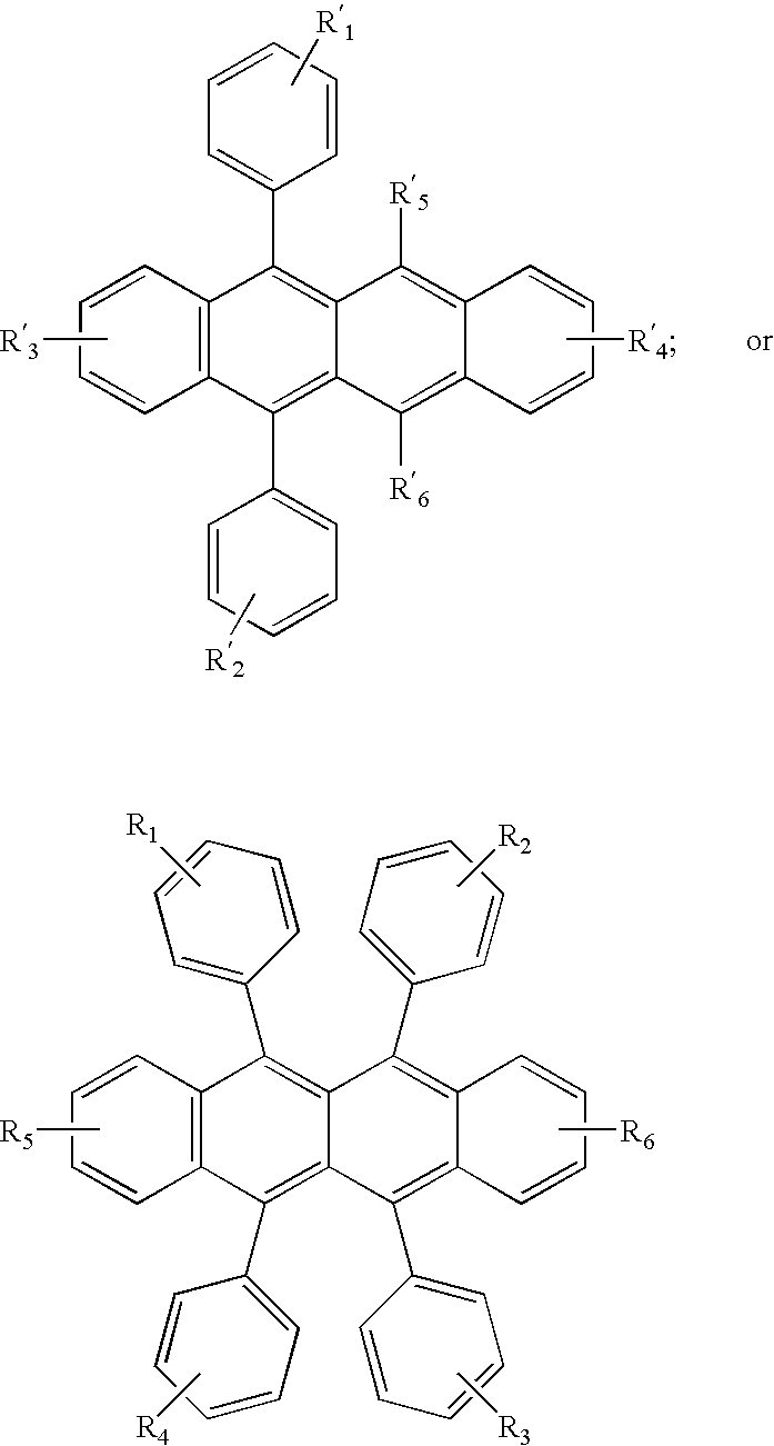
wherein R1-R6 represent one or more substituents on each ring and where each substituent is individually selected from one of the following:
- Category 1: hydrogen, or alkyl of from 1 to 24 carbon atoms;
- Category 2: aryl or substituted aryl of from 5 to 20 carbon atoms;
- Category 3: hydrocarbon containing 4 to 24 carbon atoms, completing a fused aromatic ring or ring system;
- Category 4: heteroaryl or substituted heteroaryl of from 5 to 24 carbon atoms such as thiazolyl, furyl, thienyl, pyridyl, quinolinyl or other heterocyclic systems, which are bonded via a single bond, or complete a fused heteroaromatic ring system;
- Category 5: alkoxylamino, alkylamino, or arylamino of from 1 to 24 carbon atoms; or
- Category 6: fluoro, chloro, bromo or cyano.

wherein X1-X16 are independently selected as hydrogen or substituents that include alkyl groups of from 1 to 24 carbon atoms; aryl or substituted aryl groups of from 5 to 20 carbon atoms; hydrocarbon groups containing 4 to 24 carbon atoms that complete one or more fused aromatic rings or ring systems; or halogen, provided that the substituents are selected to provide a full width at half maximum of between 5 nm and 90 nm contained within the wavelength range of 560 nm and 700 nm.


wherein:
- substituent groups R1 and R2 are independently alkyl, alkoxyl, aryl, or heteroaryl; and
- substituent groups R3 through R12 are independently hydrogen, alkyl, alkoxyl, halogen, aryl, or heteroaryl, and adjacent substituent groups R3 through R10 can optionally be connected to form one or more ring systems, including fused aromatic and fused heteroaromatic rings, provided that the substituents are selected to provide a full width at half maximum of between 5 nm and 70 nm contained within the wavelength range of 490 nm and 580 nm. Alkyl, alkoxyl, aryl, heteroaryl, fused aromatic ring and fused heteroaromatic ring substituent groups can be further substituted. Conveniently, R1 and R2 are aryl, and R2 through R12 are hydrogen, or substituent groups that are more electron withdrawing than methyl. Some examples of useful quinacridones include those disclosed in U.S. Pat. No. 5,593,788 and in U.S. Patent Application Publication 2004/0001969 A1.


wherein X is O or S, R1, R2, R3 and R6 can individually be hydrogen, alkyl, or aryl; and
- R4 and R5 can individually be alkyl or aryl, or where either R3 and R4, or R5 and R6, or both together represent the atoms completing a cycloalkyl group, provided that the substituents are selected to provide a full width at half maximum of between 5 nm and 70 nm contained within the wavelength range of 490 nm and 580 nm.


wherein:
- A and A′ represent independent azine ring systems corresponding to 6-membered aromatic ring systems containing at least one nitrogen;
- (Xa)n and (Xb)m represent one or more independently selected substituents and include acyclic substituents or are joined to form a ring fused to A or A′;
- m and n are independently 0 to 4;
- Za and Zb are independently selected substituents;
- 1, 2, 3, 4, 1′, 2′, 3′, and 4′ are independently selected as either carbon or nitrogen atoms; and
- provided that Xa, Xb, Za, and Zb, 1, 2, 3, 4, 1′, 2′, 3′, and 4′ are selected to provide a full width at half maximum of between 5 nm and 25 nm contained within a wavelength range of 400 nm and 490 nm.


2Σn i L i+2n s L s+(Q m1 +Q m2)λ/2π=mλ Eq. 1
wherein:
- ni is the refractive index and Li is the thickness of the ith sub-layer in the microcavity structure of
microcavity pixel 10; - ns is the refractive index and Ls is the thickness, which can be zero, of the
cavity spacer layer 30; - Qm1 and Qm2 are the phase shifts in radians at the two organic EL element-reflector interfaces, respectively;
- λ is the predetermined wavelength of on-axis light to be enhanced by the microcavity structure; and
- m is a non-negative integer.
For example, one can select the microcavity effect to enhance on-axis the emission of green light for a desired on-axis viewed color.
- 1. A clean glass substrate was deposited by sputtering with indium tin oxide (ITO) to form a transparent electrode of 85 nm thickness;
- 2. The above-prepared ITO surface was treated with a plasma oxygen etch, followed by plasma deposition of a 0.1 nm layer of a fluorocarbon polymer (CFx) as described in U.S. Pat. No. 6,208,075;
- 3. The above-prepared substrate was further treated by vacuum-depositing a 170 nm layer of 4,4′-bis[N-(1-naphthyl)-N-phenylamino]biphenyl (NPB) as a hole-transporting layer (HTL);
- 4. A 30 nm layer of 24 nm NPB and 6 nm 5,12-bis(t-butylphenyl)naphthacene (tBuDPN) containing 3% 6,11-diphenyl-5,12-bis(4-(6-methyl-benzothiazol-2-yl)phenyl)naphthacene (DBzR) was vacuum-deposited onto the substrate at a coating station that included a heated graphite boat source to form a yellow-light-emitting layer (yellow LEL);
- 5. A coating of 37 nm of 2-tert-butyl-9,10-bis(2-naphthyl)anthracene (TBADN) with 3 nm NPB and 2.5% 4-(di-p-tolylamino)-4′-[(di-p-tolylamino)styryl]stilbene (TPDBP above) was evaporatively deposited on the above substrate to form a blue-light-emitting layer (blue LEL);
- 6. A 10 nm electron-transporting layer (ETL) of tris(8-quinolinolato)aluminum (III) (ALQ) was vacuum-deposited onto the substrate at a coating station that included a heated tantalum boat source; and
- 7. A 0.5 nm layer of lithium fluoride was evaporatively deposited onto the substrate, followed by a 100 nm layer of aluminum, to form a cathode layer.
- 1. A clean glass substrate was deposited by sputtering with indium tin oxide (ITO) to form a transparent electrode of 85 nm thickness;
- 2. The above-prepared ITO surface was treated with a plasma oxygen etch, followed by plasma deposition of a 0.1 nm layer of a fluorocarbon polymer (CFx) as described in U.S. Pat. No. 6,208,075;
- 3. The above-prepared substrate was further treated by vacuum-depositing a 240 nm layer of NPB as a hole-transporting layer (HTL);
- 4. A 28 nm layer of 20 nm NPB and 8 nm rubrene containing 0.5% TPDPB (above) was vacuum-deposited onto the substrate at a coating station that included a heated graphite boat source to form a red light-emitting layer (red LEL);
- 5. A coating of 20 nm of 2-tert-butyl-9,10-bis(2-naphthyl)anthracene (TBADN) with 1 nm NPB and 0.75% BEP (above) was evaporatively deposited on the above substrate to form a blue-light-emitting layer (blue LEL);
- 6. A 15 nm layer of ALQ containing 0.5% diphenylquinacridone (DPQA) was evaporatively deposited on the above substrate to form a green light-emitting layer (green LEL);
- 7. A 15 nm electron-transporting layer (ETL) of ALQ was vacuum-deposited onto the substrate at a coating station that included a heated graphite boat source; and
- 8. A 0.5 nm layer of lithium fluoride was evaporatively deposited onto the substrate, followed by a 100 nm layer of aluminum, to form a cathode layer.
- 4. A 27 nm layer of 20 nm NPB and 7 nm rubrene containing 0.5% TPDPB (above) was vacuum-deposited onto the substrate at a coating station that included a heated graphite boat source to form a red light-emitting layer (red LEL);
- 5. A coating of 40 nm of TBADN with 0.5% DPQA was evaporatively deposited on the above substrate to form a green-light-emitting layer (green LEL);
- 6. A coating of 20 nm of TBADN with 1 nm NPB and 0.75% BEP was evaporatively deposited on the above substrate to form a blue-light-emitting layer (blue LEL); and
- 7. A 20 nm electron-transporting layer (ETL) of ALQ was vacuum-deposited onto the substrate at a coating station that included a heated graphite boat source.
- 3. The above-prepared substrate was further treated by vacuum-depositing a 120 nm layer of NPB as a hole-transporting layer (HTL);
- 4. A 27 nm layer of 20 nm NPB and 7 nm rubrene containing 0.5% TPDPB (above) was vacuum-deposited onto the substrate at a coating station that included a heated graphite boat source to form a red light-emitting layer (red LEL);
- 5. A coating of 10 nm of TBADN and 10 nm ALQ with 0.5% DPQA was evaporatively deposited on the above substrate to form a green-light-emitting layer (green LEL);
- 6. A coating of 20 nm of TBADN with 1 nm NPB and 0.75% BEP was evaporatively deposited on the above substrate to form a blue-light-emitting layer (blue LEL); and
- 7. A 20 nm electron-transporting layer (ETL) of ALQ was vacuum-deposited onto the substrate at a coating station that included a heated graphite boat source.
| TABLE 1 | |||||
| Example 1 | Example 2 | Example 3 | Example 4 | ||
| (Comparative) | (Inventive) | (Inventive) | (Inventive) | ||
| Red dopant | — | 0.5% TPDPB | 0.5% TPDPB | 0.5% TPDPB |
| Yellow dopant | 3% DBzR | — | — | — |
| Green dopant | — | 0.5% DPQA | 0.5% DPQA | 0.5% DPQA |
| Green host | — | ALQ | TBADN | TBADN/ALQ |
| Blue dopant | 2.5% L47 | 0.75% BEP | 0.75% BEP | 0.75% BEP |
| Emitting layer order (bottom to top) | YB | RBG | RGB | RGB |
| Relative White Luminous Efficiency | 1 | 0.54 | 0.72 | 0.63 |
| Relative lifetime | 1 | 4.5 | 3.5 | 3.0 |
| Relative Power Consumption | 1 | 1.73 | 1.19 | 1.19 |
| Red λmax | 572 | nm | 604 | nm | 608 | nm | 608 | nm |
| Red full width at half maximum | 84 | nm | 28 | nm | 28 | nm | 28 | nm |
| Red FWHM Range | 546–630 | nm | 592–620 | nm | 592–620 | nm | 592–620 | nm |
| Green λmax | — | 508 | nm | 516 | nm | 520 | nm |
| Green full width at half maximum | — | 32 | nm | 28 | nm | 28 | nm |
| Green FWHM Range | — | 511–543 | nm | 504–532 | nm | 507–535 | nm |
| Blue λmax | 472 | nm | 452 | nm | 452 | nm | 452 | nm |
| Blue full width at half maximum | 60 | nm | 12 | nm | 12 | nm | 12 | nm |
| Blue FWHM Range | 460–520 | nm | 446–458 | nm | 446–458 | nm | 446–458 | nm |
Delta CIEx,y=√{square root over ([(CIEx 0° −CIEx 60°)2+(CIEy 0° −CIEy 60°)2])}{square root over ([(CIEx 0° −CIEx 60°)2+(CIEy 0° −CIEy 60°)2])}.
| TABLE 2 | |||||
| Example 1 | Example 2 | Example 3 | Example 4 | ||
| (Comparative) | (Inventive) | (Inventive) | (Inventive) | ||
| Red (CIEx, y) | 0.623, 0.371 | 0.638, 0.354 | 0.630, 0.339 | 0.635, 0.348 |
| Red CIEx, y change at 60° viewing | 0.06 | 0.07 | 0.09 | 0.08 |
| angle | ||||
| Relative red luminous efficiency | 1 | 0.56 | 0.45 | 0.67 |
| Red luminous efficiency loss at 60° | 86% | 90% | 71% | 87% |
| viewing angle | ||||
| Green (CIEx, y) | 0.329, 0.627 | 0.262, 0.690 | 0.157, 0.721 | 0.203, 0.713 |
| Green CIEx, y change at 60° viewing | 0.21 | 0.16 | 0.25 | 0.16 |
| angle | ||||
| Relative green luminous efficiency | 1 | 0.61 | 0.98 | 0.77 |
| Green luminous efficiency loss at 60° | 66% | 71% | 72% | 52% |
| viewing angle | ||||
| Blue (CIEx, y) | 0.120, 0.100 | 0.144, 0.063 | 0.137, 0.077 | 0.144, 0.059 |
| Blue CIEx, y change at 60° viewing | 0.02 | 0.03 | 0.04 | 0.02 |
| angle | ||||
| Relative blue luminous efficiency | 1 | 0.35 | 0.93 | 0.58 |
| Blue luminous efficiency loss at 60° | 71% | 56% | 46% | 83% |
| viewing angle | ||||
| White (CIEx, y) | 0.355, 0.399 | 0.364, 0.369 | 0.260, 0.322 | 0.274, 0.336 |
| White CIEx, y change at 60° viewing | 0.12 | 0.12 | 0.09 | 0.13 |
| angle | ||||
| White luminance loss at 60° viewing | 73% | 75% | 72% | 64% |
| angle | ||||
- 10 microcavity pixel
- 10 a microcavity pixel
- 10 b micro cavity pixel
- 10 c micro cavity pixel
- 15 color OLED display
- 20 substrate
- 25 semitransparent reflector
- 25 a semitransparent reflector
- 25 b semitransparent reflector
- 25 c semitransparent reflector
- 30 cavity spacer layer
- 30 a cavity spacer layer
- 30 b cavity spacer layer
- 35 hole-injecting layer
- 40 hole-transporting layer
- 45 first light-emitting layer
- 50 second light-emitting layer
- 55 third light-emitting layer
- 60 electron-transporting layer
- 65 electron-injecting layer
- 70 organic EL element
- 90 reflector
- 105 λmax
- 110 full width at half maximum
- 115 color gamut
- 120 color gamut
- 125 color gamut
- 130 color gamut
Claims (36)


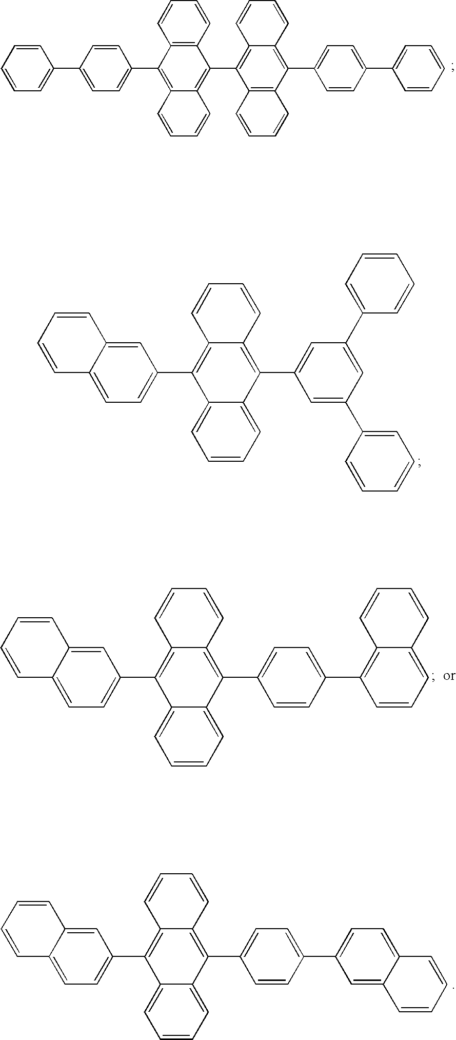
Priority Applications (3)
| Application Number | Priority Date | Filing Date | Title |
|---|---|---|---|
| US10/838,665 US7247394B2 (en) | 2004-05-04 | 2004-05-04 | Tuned microcavity color OLED display |
| PCT/US2005/013959 WO2005116969A2 (en) | 2004-05-04 | 2005-04-25 | Improved tuned microcavity color oled display |
| TW094114169A TWI364448B (en) | 2004-05-04 | 2005-05-03 | Improved tuned microcavity color oled display |
Applications Claiming Priority (1)
| Application Number | Priority Date | Filing Date | Title |
|---|---|---|---|
| US10/838,665 US7247394B2 (en) | 2004-05-04 | 2004-05-04 | Tuned microcavity color OLED display |
Publications (2)
| Publication Number | Publication Date |
|---|---|
| US20050249972A1 US20050249972A1 (en) | 2005-11-10 |
| US7247394B2 true US7247394B2 (en) | 2007-07-24 |
Family
ID=35239780
Family Applications (1)
| Application Number | Title | Priority Date | Filing Date |
|---|---|---|---|
| US10/838,665 Active 2025-06-12 US7247394B2 (en) | 2004-05-04 | 2004-05-04 | Tuned microcavity color OLED display |
Country Status (3)
| Country | Link |
|---|---|
| US (1) | US7247394B2 (en) |
| TW (1) | TWI364448B (en) |
| WO (1) | WO2005116969A2 (en) |
Cited By (41)
| Publication number | Priority date | Publication date | Assignee | Title |
|---|---|---|---|---|
| US20060091380A1 (en) * | 2004-10-25 | 2006-05-04 | Canon Kabushiki Kaisha | Organic light-emitting device array and display |
| US20060139255A1 (en) * | 2004-10-13 | 2006-06-29 | Kim Yang W | Organic light emitting display |
| US20080176099A1 (en) * | 2007-01-18 | 2008-07-24 | Hatwar Tukaram K | White oled device with improved functions |
| US20080308037A1 (en) * | 2007-06-14 | 2008-12-18 | Massachusetts Institute Of Technology | Method and apparatus for thermal jet printing |
| US20090053559A1 (en) * | 2007-08-20 | 2009-02-26 | Spindler Jeffrey P | High-performance broadband oled device |
| US20090053557A1 (en) * | 2007-08-23 | 2009-02-26 | Spindler Jeffrey P | Stabilized white-emitting oled device |
| US20090231243A1 (en) * | 2008-03-13 | 2009-09-17 | Samsung Mobile Display Co., Ltd. | Organic light-emitting display apparatus and method of manufacturing the same |
| US20090266978A1 (en) * | 2008-04-23 | 2009-10-29 | Micron Technology, Inc. | Method and apparatus providing color filter array with non-uniform color filter sizes |
| US20100013383A1 (en) * | 2008-07-17 | 2010-01-21 | Samsung Electronics Co., Ltd. | Organic light emitting device and manufacturing method thereof |
| US20100053044A1 (en) * | 2008-09-01 | 2010-03-04 | Lee Hae-Yeon | Organic light emitting diode display and method for manufacturing the same |
| US20100171780A1 (en) * | 2009-01-05 | 2010-07-08 | Kateeva, Inc. | Rapid Ink-Charging Of A Dry Ink Discharge Nozzle |
| US20100201749A1 (en) * | 2008-06-13 | 2010-08-12 | Kateeva, Inc. | Method And Apparatus for Load-Locked Printing |
| WO2010114749A1 (en) | 2009-04-03 | 2010-10-07 | Global Oled Technology Llc | Tandem white oled with efficient electron transfer |
| DE102009022408A1 (en) * | 2009-05-18 | 2010-12-09 | Technische Universität Dresden | Organic solar cell or photodetector with improved absorption |
| US20110008541A1 (en) * | 2009-05-01 | 2011-01-13 | Kateeva, Inc. | Method and apparatus for organic vapor printing |
| US20110062475A1 (en) * | 2009-09-15 | 2011-03-17 | Cho Jae-Young | Organic light emitting display device |
| US20110170184A1 (en) * | 2010-01-13 | 2011-07-14 | Wolk Martin B | Microreplicated Film for Attachment to Autostereoscopic Display Components |
| US20120319147A1 (en) * | 2011-06-14 | 2012-12-20 | Hee-Joo Ko | Organic light emitting diode display |
| US8469551B2 (en) | 2010-10-20 | 2013-06-25 | 3M Innovative Properties Company | Light extraction films for increasing pixelated OLED output with reduced blur |
| US8547015B2 (en) | 2010-10-20 | 2013-10-01 | 3M Innovative Properties Company | Light extraction films for organic light emitting devices (OLEDs) |
| US8556389B2 (en) | 2011-02-04 | 2013-10-15 | Kateeva, Inc. | Low-profile MEMS thermal printhead die having backside electrical connections |
| US8632145B2 (en) | 2008-06-13 | 2014-01-21 | Kateeva, Inc. | Method and apparatus for printing using a facetted drum |
| US8692446B2 (en) | 2011-03-17 | 2014-04-08 | 3M Innovative Properties Company | OLED light extraction films having nanoparticles and periodic structures |
| US20140319483A1 (en) * | 2013-04-26 | 2014-10-30 | Samsung Display Co., Ltd. | Organic light emitting diode display |
| US8899171B2 (en) | 2008-06-13 | 2014-12-02 | Kateeva, Inc. | Gas enclosure assembly and system |
| US8986780B2 (en) | 2004-11-19 | 2015-03-24 | Massachusetts Institute Of Technology | Method and apparatus for depositing LED organic film |
| US9005365B2 (en) | 2004-11-19 | 2015-04-14 | Massachusetts Institute Of Technology | Method and apparatus for depositing LED organic film |
| US9047891B1 (en) * | 2014-05-03 | 2015-06-02 | HGST Netherlands B.V. | Current-perpendicular-to-the-plane giant magnetoresistance (CPP-GMR) sensor with indium-zinc-oxide (IZO) spacer layer |
| US9048344B2 (en) | 2008-06-13 | 2015-06-02 | Kateeva, Inc. | Gas enclosure assembly and system |
| US9331302B2 (en) | 2014-02-18 | 2016-05-03 | Industrial Technology Research Institute | Blue light emitting device and light emitting device |
| US9559326B2 (en) | 2015-01-26 | 2017-01-31 | Industrial Technology Research Institute | Light emitting element |
| US9604245B2 (en) | 2008-06-13 | 2017-03-28 | Kateeva, Inc. | Gas enclosure systems and methods utilizing an auxiliary enclosure |
| US20170194385A1 (en) * | 2015-12-30 | 2017-07-06 | Lg Display Co., Ltd. | Organic light-emitting diode display device |
| US9704924B2 (en) | 2015-01-26 | 2017-07-11 | Industrial Technology Research Institute | Light emitting device |
| US9741959B1 (en) | 2016-02-19 | 2017-08-22 | Industrial Technology Research Institute | Light emitting device |
| US20170294488A1 (en) * | 2016-04-11 | 2017-10-12 | Abl Ip Holding Llc | Luminaire utilizing a transparent organic light emitting device display |
| US11107712B2 (en) | 2013-12-26 | 2021-08-31 | Kateeva, Inc. | Techniques for thermal treatment of electronic devices |
| US11164911B2 (en) | 2017-09-28 | 2021-11-02 | Apple Inc. | Displays with white organic light-emitting diodes |
| US11338319B2 (en) | 2014-04-30 | 2022-05-24 | Kateeva, Inc. | Gas cushion apparatus and techniques for substrate coating |
| US11489119B2 (en) | 2014-01-21 | 2022-11-01 | Kateeva, Inc. | Apparatus and techniques for electronic device encapsulation |
| US11633968B2 (en) | 2008-06-13 | 2023-04-25 | Kateeva, Inc. | Low-particle gas enclosure systems and methods |
Families Citing this family (88)
| Publication number | Priority date | Publication date | Assignee | Title |
|---|---|---|---|---|
| JPWO2005002010A1 (en) * | 2003-06-27 | 2006-08-10 | 株式会社半導体エネルギー研究所 | Organic laser equipment |
| US20050008052A1 (en) * | 2003-07-01 | 2005-01-13 | Ryoji Nomura | Light-emitting device |
| US20050147844A1 (en) * | 2004-01-05 | 2005-07-07 | Eastman Kodak Company | White oled devices with color filter arrays |
| US7300709B2 (en) * | 2004-03-31 | 2007-11-27 | Eastman Kodak Company | Organic element for electroluminescent devices |
| TWI327563B (en) * | 2004-05-24 | 2010-07-21 | Au Optronics Corp | Anthracene compound and organic electroluminescent device including the anthracene compound |
| US7315118B2 (en) * | 2004-05-28 | 2008-01-01 | Au Optronics Corporation | Combinational structures for electro-luminescent displays |
| CN100531498C (en) * | 2004-05-31 | 2009-08-19 | 株式会社丰田自动织机 | Organic EL device |
| KR20060046476A (en) * | 2004-06-18 | 2006-05-17 | 산요덴키가부시키가이샤 | Electro-luminescence panel |
| KR100611756B1 (en) * | 2004-06-18 | 2006-08-10 | 삼성에스디아이 주식회사 | Organic electroluminescent display device and method of fabricating the same |
| EP1784056B1 (en) * | 2004-07-23 | 2011-04-13 | Konica Minolta Holdings, Inc. | Organic electroluminescent device, display and illuminating device |
| JP4966203B2 (en) * | 2004-12-24 | 2012-07-04 | シーディーティー オックスフォード リミテッド | Light emitting device |
| WO2006093007A1 (en) * | 2005-03-02 | 2006-09-08 | Konica Minolta Holdings, Inc. | Organic electroluminescence element, image display unit and lighting device |
| US7851989B2 (en) * | 2005-03-25 | 2010-12-14 | Semiconductor Energy Laboratory Co., Ltd. | Light emitting device |
| TWI257267B (en) * | 2005-03-31 | 2006-06-21 | Au Optronics Corp | Organic electroluminescent display panel |
| US8729795B2 (en) | 2005-06-30 | 2014-05-20 | Semiconductor Energy Laboratory Co., Ltd. | Light emitting device and electronic device |
| KR100708714B1 (en) * | 2005-09-30 | 2007-04-17 | 삼성에스디아이 주식회사 | Organic light emitting display device and manufacturing method thereof |
| JP4281754B2 (en) * | 2006-03-27 | 2009-06-17 | セイコーエプソン株式会社 | Organic EL compound and organic EL device |
| JP2007265763A (en) * | 2006-03-28 | 2007-10-11 | Canon Inc | Full-color organic electroluminescent panel |
| JP4211799B2 (en) * | 2006-04-13 | 2009-01-21 | セイコーエプソン株式会社 | Organic EL compound and organic EL device |
| US8277955B2 (en) * | 2006-10-17 | 2012-10-02 | Seiko Epson Corporation | Compound for organic EL device and organic EL device |
| KR100823511B1 (en) * | 2006-11-10 | 2008-04-21 | 삼성에스디아이 주식회사 | Organic light emission display and fabrication method thereof |
| JP2008146904A (en) * | 2006-12-07 | 2008-06-26 | Sony Corp | Organic electroluminescent element and display device |
| JP4254886B2 (en) | 2006-12-22 | 2009-04-15 | ソニー株式会社 | Organic electroluminescence device and display device |
| US20080164809A1 (en) * | 2006-12-22 | 2008-07-10 | Sony Corporation | Organic electroluminescent device and display apparatus |
| DE112008000348B4 (en) * | 2007-02-05 | 2017-06-22 | Lg Display Co., Ltd. | Organic light emitting device with improved light emission efficiency and method of making the same |
| US7728512B2 (en) * | 2007-03-02 | 2010-06-01 | Universal Display Corporation | Organic light emitting device having an external microcavity |
| JP4811314B2 (en) * | 2007-03-27 | 2011-11-09 | セイコーエプソン株式会社 | Organic EL device |
| US20080238297A1 (en) * | 2007-03-29 | 2008-10-02 | Masuyuki Oota | Organic el display and method of manufacturing the same |
| US20080286610A1 (en) * | 2007-05-17 | 2008-11-20 | Deaton Joseph C | Hybrid oled with fluorescent and phosphorescent layers |
| JP5167723B2 (en) * | 2007-08-21 | 2013-03-21 | セイコーエプソン株式会社 | Light emitting device |
| KR101434361B1 (en) * | 2007-10-16 | 2014-08-26 | 삼성디스플레이 주식회사 | White organic light emitting device and color display apparatus employing the same |
| JP2009111023A (en) * | 2007-10-26 | 2009-05-21 | Toshiba Matsushita Display Technology Co Ltd | Organic el display device and manufacturing method thereof |
| US8877350B2 (en) * | 2007-12-11 | 2014-11-04 | Global Oled Technology Llc | White OLED with two blue light-emitting layers |
| JP2009170127A (en) * | 2008-01-11 | 2009-07-30 | Seiko Epson Corp | Light emitting device, and electronic apparatus |
| EP2249410B1 (en) * | 2008-02-25 | 2015-12-02 | Samsung Electronics Co., Ltd. | Organic electroluminescent element, and manufacturing method and uses therefor |
| JP5491383B2 (en) * | 2008-03-19 | 2014-05-14 | 出光興産株式会社 | Anthracene derivatives, light emitting materials, and organic electroluminescence devices |
| TWI470787B (en) * | 2008-03-31 | 2015-01-21 | Japan Display Inc | Organic el display device and method of manufacturing the same |
| JP4775863B2 (en) | 2008-09-26 | 2011-09-21 | 東芝モバイルディスプレイ株式会社 | Organic EL display device and manufacturing method thereof |
| KR101582937B1 (en) * | 2008-12-02 | 2016-01-08 | 삼성디스플레이 주식회사 | Organic light emitting diode display and method for manufacturing the same |
| KR20100071539A (en) * | 2008-12-19 | 2010-06-29 | 삼성전자주식회사 | Organic light emitting device and method for manufacturing the same |
| JP5164825B2 (en) * | 2008-12-19 | 2013-03-21 | キヤノン株式会社 | Organic light emitting device |
| JP4775865B2 (en) * | 2009-01-14 | 2011-09-21 | 東芝モバイルディスプレイ株式会社 | Organic EL display device and manufacturing method thereof |
| JP5457847B2 (en) * | 2009-01-23 | 2014-04-02 | ユー・ディー・シー アイルランド リミテッド | Organic electroluminescence device |
| JP2011029172A (en) * | 2009-06-30 | 2011-02-10 | Fujifilm Corp | Organic el device, and design method thereof |
| JP5268840B2 (en) * | 2009-09-10 | 2013-08-21 | 株式会社東芝 | Organic electroluminescence device |
| US20110108812A1 (en) * | 2009-11-06 | 2011-05-12 | Shiro Sumita | Organic el device |
| KR101182442B1 (en) * | 2010-01-27 | 2012-09-12 | 삼성디스플레이 주식회사 | OLED display apparatus and Method thereof |
| JP2011191739A (en) * | 2010-02-16 | 2011-09-29 | Toshiba Mobile Display Co Ltd | Organic electroluminescence device |
| KR20120005793A (en) * | 2010-07-09 | 2012-01-17 | 삼성모바일디스플레이주식회사 | Display device |
| US9691983B2 (en) * | 2010-07-16 | 2017-06-27 | Sumitomo Chemical Company, Limited | Composition containing polymer compound and light-emitting device using the same |
| KR101983229B1 (en) * | 2010-07-23 | 2019-05-29 | 삼성디스플레이 주식회사 | Organic light emitting device and method for manufacturing the same |
| CN103178084B (en) * | 2011-12-23 | 2015-10-14 | 乐金显示有限公司 | Organic light-emitting display device |
| KR101918953B1 (en) * | 2012-03-06 | 2018-11-16 | 삼성디스플레이 주식회사 | Amine-based compound, organic light emitting diode comprising the same and organic light emitting apparatus comprising the same |
| JP2014026902A (en) * | 2012-07-30 | 2014-02-06 | Sony Corp | Display device, method for manufacturing display device, and electronic apparatus |
| KR102009726B1 (en) * | 2012-11-08 | 2019-10-22 | 삼성디스플레이 주식회사 | Organic light emitting display apparatus and method for manufacturing the same |
| KR102016068B1 (en) * | 2012-11-30 | 2019-08-29 | 엘지디스플레이 주식회사 | Organic light emitting display |
| JP6111643B2 (en) * | 2012-12-17 | 2017-04-12 | セイコーエプソン株式会社 | ORGANIC ELECTROLUMINESCENCE DEVICE AND ELECTRONIC DEVICE |
| KR102046157B1 (en) * | 2012-12-21 | 2019-12-03 | 삼성디스플레이 주식회사 | Organic light emitting diode display and manufacturing method thereof |
| KR102050484B1 (en) | 2013-03-04 | 2019-12-02 | 삼성디스플레이 주식회사 | Anthracene derivatives and organic light emitting diodes comprising the derivatives |
| KR102081209B1 (en) * | 2013-03-26 | 2020-02-26 | 삼성디스플레이 주식회사 | Organic light emitting display device and manufacturing method thereof, and donor substrate, donor substrate set using manufacturing organic light emitting display device thereof |
| CN104078612A (en) * | 2013-03-29 | 2014-10-01 | 海洋王照明科技股份有限公司 | White organic light-emitting diode and manufacturing method thereof |
| KR102107106B1 (en) | 2013-05-09 | 2020-05-07 | 삼성디스플레이 주식회사 | Styryl-based compound and organic light emitting diode comprising the same |
| JP6564559B2 (en) * | 2013-05-10 | 2019-08-21 | 株式会社半導体エネルギー研究所 | Display panel and electronic equipment |
| KR102269131B1 (en) * | 2013-07-01 | 2021-06-25 | 삼성디스플레이 주식회사 | Compound and organic light emitting device comprising same |
| JP6207263B2 (en) * | 2013-07-03 | 2017-10-04 | 株式会社ジャパンディスプレイ | Organic EL display device and manufacturing method thereof |
| JP6196086B2 (en) * | 2013-07-19 | 2017-09-13 | 株式会社小糸製作所 | Organic EL panel and vehicle lamp |
| KR102053443B1 (en) | 2013-10-23 | 2019-12-06 | 엘지디스플레이 주식회사 | Organic light emitting device |
| CN104681743B (en) * | 2013-11-29 | 2017-02-15 | 清华大学 | Preparation method of organic light emitting diode |
| US10062850B2 (en) | 2013-12-12 | 2018-08-28 | Samsung Display Co., Ltd. | Amine-based compounds and organic light-emitting devices comprising the same |
| JP2015122459A (en) * | 2013-12-25 | 2015-07-02 | 三星ディスプレイ株式會社Samsung Display Co.,Ltd. | Organic EL element |
| CN104851980B (en) * | 2014-02-13 | 2017-02-08 | 上海和辉光电有限公司 | Full-color organic light-emitting diode structure |
| KR20150132795A (en) | 2014-05-16 | 2015-11-26 | 삼성디스플레이 주식회사 | Organic light emitting device |
| KR102327086B1 (en) | 2014-06-11 | 2021-11-17 | 삼성디스플레이 주식회사 | Organic light-emitting devices |
| KR102245164B1 (en) * | 2014-08-22 | 2021-04-27 | 엘지디스플레이 주식회사 | Organic light emitting device and method of fabricating the same |
| CN104466027B (en) * | 2014-12-30 | 2017-03-08 | 昆山国显光电有限公司 | The micro-cavity structure of OLED and OLED |
| KR102343145B1 (en) | 2015-01-12 | 2021-12-27 | 삼성디스플레이 주식회사 | Condensed compound and organic light-emitting device comprising the same |
| JP6707804B2 (en) * | 2015-09-24 | 2020-06-10 | エルジー・ケム・リミテッド | Compound and organic light emitting device containing the same |
| US10756141B2 (en) | 2016-07-28 | 2020-08-25 | Universal Display Corporation | Very high resolution stacked OLED display |
| CN106207015B (en) * | 2016-09-20 | 2018-05-25 | 昆山国显光电有限公司 | A kind of method for blocking the common layer lateral cross talk of OLED luminescent devices |
| KR102512378B1 (en) * | 2017-02-16 | 2023-03-20 | 가꼬우 호징 관세이 가쿠잉 | organic electroluminescent device |
| WO2019095380A1 (en) * | 2017-11-20 | 2019-05-23 | 深圳市柔宇科技有限公司 | Quantum-dot electroluminescent component, preparation method therefor, and display device |
| CN108075047A (en) * | 2017-12-11 | 2018-05-25 | 合肥京东方光电科技有限公司 | Organic light emitting diode device and its manufacturing method, display panel |
| US11917840B2 (en) | 2018-05-18 | 2024-02-27 | Semiconductor Energy Laboratory Co., Ltd. | Light-emitting device with reflective electrode and light-emitting layer |
| CN109830516B (en) | 2019-02-22 | 2021-11-12 | 京东方科技集团股份有限公司 | OLED substrate and display device |
| CN109904348B (en) | 2019-03-18 | 2021-01-12 | 京东方科技集团股份有限公司 | Pixel unit, display panel and display device |
| US11495777B2 (en) * | 2019-09-30 | 2022-11-08 | Joled Inc. | Self-luminous element, self-luminous panel, and self-luminous panel manufacturing method |
| CN110797385B (en) * | 2019-12-03 | 2022-04-12 | 上海天马微电子有限公司 | Display panel, display device and preparation method |
| US11937478B2 (en) | 2021-07-16 | 2024-03-19 | Avalon Holographics Inc. | Multi-colored microcavity OLED array having DBR for high aperture display and method of fabricating the same |
Citations (18)
| Publication number | Priority date | Publication date | Assignee | Title |
|---|---|---|---|---|
| US4769292A (en) | 1987-03-02 | 1988-09-06 | Eastman Kodak Company | Electroluminescent device with modified thin film luminescent zone |
| US4885211A (en) | 1987-02-11 | 1989-12-05 | Eastman Kodak Company | Electroluminescent device with improved cathode |
| US5405709A (en) | 1993-09-13 | 1995-04-11 | Eastman Kodak Company | White light emitting internal junction organic electroluminescent device |
| US5405710A (en) | 1993-11-22 | 1995-04-11 | At&T Corp. | Article comprising microcavity light sources |
| JPH07142169A (en) | 1993-11-15 | 1995-06-02 | Mitsubishi Chem Corp | Organic electroluminescence element |
| US5554911A (en) | 1993-03-18 | 1996-09-10 | Hitachi, Ltd. | Light-emitting elements |
| US5683823A (en) | 1996-01-26 | 1997-11-04 | Eastman Kodak Company | White light-emitting organic electroluminescent devices |
| US5708174A (en) | 1992-03-12 | 1998-01-13 | Smithkline Beecham P.L.C. | Heterocyclic-esters or -amides used as 5-HT4 receptor antagonists |
| JPH11288786A (en) | 1998-02-04 | 1999-10-19 | Toyota Central Res & Dev Lab Inc | Optical resonance type organic electroluminescence element |
| US6281634B1 (en) | 1998-12-01 | 2001-08-28 | Sanyo Electric Co., Ltd. | Color electroluminescence display device |
| US6392340B2 (en) | 1998-02-27 | 2002-05-21 | Sanyo Electric Co., Ltd. | Color display apparatus having electroluminescence elements |
| US20020186214A1 (en) | 2001-06-05 | 2002-12-12 | Eastman Kodak Company | Method for saving power in an organic electroluminescent display using white light emitting elements |
| EP1286569A1 (en) | 2001-08-15 | 2003-02-26 | Eastman Kodak Company | White organic light-emitting devices with improved efficiency |
| EP1340798A2 (en) | 2002-02-28 | 2003-09-03 | Eastman Kodak Company | Organic element for electroluminescent devices |
| EP1375624A1 (en) | 2002-06-27 | 2004-01-02 | Eastman Kodak Company | Device containing green organic light-emitting diode |
| EP1450419A2 (en) | 2003-02-18 | 2004-08-25 | Eastman Kodak Company | Tuned microcavity color oled display |
| WO2005060016A2 (en) | 2003-10-07 | 2005-06-30 | Eastman Kodak Company | White-emitting microcavity oled device |
| WO2005101541A1 (en) | 2004-04-07 | 2005-10-27 | Eastman Kodak Company | Color oled with added color gamut pixels |
-
2004
- 2004-05-04 US US10/838,665 patent/US7247394B2/en active Active
-
2005
- 2005-04-25 WO PCT/US2005/013959 patent/WO2005116969A2/en active Application Filing
- 2005-05-03 TW TW094114169A patent/TWI364448B/en active
Patent Citations (20)
| Publication number | Priority date | Publication date | Assignee | Title |
|---|---|---|---|---|
| US4885211A (en) | 1987-02-11 | 1989-12-05 | Eastman Kodak Company | Electroluminescent device with improved cathode |
| US4769292A (en) | 1987-03-02 | 1988-09-06 | Eastman Kodak Company | Electroluminescent device with modified thin film luminescent zone |
| US5708174A (en) | 1992-03-12 | 1998-01-13 | Smithkline Beecham P.L.C. | Heterocyclic-esters or -amides used as 5-HT4 receptor antagonists |
| US5554911A (en) | 1993-03-18 | 1996-09-10 | Hitachi, Ltd. | Light-emitting elements |
| US5405709A (en) | 1993-09-13 | 1995-04-11 | Eastman Kodak Company | White light emitting internal junction organic electroluminescent device |
| JPH07142169A (en) | 1993-11-15 | 1995-06-02 | Mitsubishi Chem Corp | Organic electroluminescence element |
| US5405710A (en) | 1993-11-22 | 1995-04-11 | At&T Corp. | Article comprising microcavity light sources |
| EP0654833A1 (en) | 1993-11-22 | 1995-05-24 | AT&T Corp. | Article comprising microcavity light sources |
| US5683823A (en) | 1996-01-26 | 1997-11-04 | Eastman Kodak Company | White light-emitting organic electroluminescent devices |
| US6406801B1 (en) | 1998-02-04 | 2002-06-18 | Kabushiki Kaisha Toyota Chuo Kenkyusho | Optical resonator type organic electroluminescent element |
| JPH11288786A (en) | 1998-02-04 | 1999-10-19 | Toyota Central Res & Dev Lab Inc | Optical resonance type organic electroluminescence element |
| US6392340B2 (en) | 1998-02-27 | 2002-05-21 | Sanyo Electric Co., Ltd. | Color display apparatus having electroluminescence elements |
| US6281634B1 (en) | 1998-12-01 | 2001-08-28 | Sanyo Electric Co., Ltd. | Color electroluminescence display device |
| US20020186214A1 (en) | 2001-06-05 | 2002-12-12 | Eastman Kodak Company | Method for saving power in an organic electroluminescent display using white light emitting elements |
| EP1286569A1 (en) | 2001-08-15 | 2003-02-26 | Eastman Kodak Company | White organic light-emitting devices with improved efficiency |
| EP1340798A2 (en) | 2002-02-28 | 2003-09-03 | Eastman Kodak Company | Organic element for electroluminescent devices |
| EP1375624A1 (en) | 2002-06-27 | 2004-01-02 | Eastman Kodak Company | Device containing green organic light-emitting diode |
| EP1450419A2 (en) | 2003-02-18 | 2004-08-25 | Eastman Kodak Company | Tuned microcavity color oled display |
| WO2005060016A2 (en) | 2003-10-07 | 2005-06-30 | Eastman Kodak Company | White-emitting microcavity oled device |
| WO2005101541A1 (en) | 2004-04-07 | 2005-10-27 | Eastman Kodak Company | Color oled with added color gamut pixels |
Non-Patent Citations (4)
| Title |
|---|
| "Control of emission characteristics in organic thin-film electroluminescent diodes using an optical-microcavity structure" by Noriyuki Takada et al., Applied Physics Letter 63 (15) Oct. 11, 1993, pp. 2032-2-34. |
| "Multilayer White Light-Emitting Organic Electroluminescent Device" by Junji Kido et al., Science vol. 267, Mar. 3, 1995, pp. 1332-1334. |
| "White light-emitting organic electroluminescent devices based on interlayer sequential energy transfer" by R. S. Deshpande et al., Applied Physics Letters, vol. 75, No. 7, Aug. 16, 1999, pp. 888-890. |
| "White light-emitting organic electroluminescent devices using the poly(N-vinylcarbazole) emitter layer doped with three fluorescent dyes" by J. Kido et al., Appl. Phys. Letter 64 (7), Feb. 14, 1994, pp. 815-817. |
Cited By (70)
| Publication number | Priority date | Publication date | Assignee | Title |
|---|---|---|---|---|
| US20060139255A1 (en) * | 2004-10-13 | 2006-06-29 | Kim Yang W | Organic light emitting display |
| US8759817B2 (en) * | 2004-10-25 | 2014-06-24 | Canon Kabushiki Kaisha | Organic light-emitting device array and display |
| US20060091380A1 (en) * | 2004-10-25 | 2006-05-04 | Canon Kabushiki Kaisha | Organic light-emitting device array and display |
| US9005365B2 (en) | 2004-11-19 | 2015-04-14 | Massachusetts Institute Of Technology | Method and apparatus for depositing LED organic film |
| US8986780B2 (en) | 2004-11-19 | 2015-03-24 | Massachusetts Institute Of Technology | Method and apparatus for depositing LED organic film |
| US8962073B2 (en) | 2004-11-19 | 2015-02-24 | Massachusetts Institute Of Technology | Method and apparatus for controlling film deposition |
| US9385322B2 (en) | 2005-11-21 | 2016-07-05 | Massachusetts Institute Of Technology | Method and apparatus for depositing LED organic film |
| US20080176099A1 (en) * | 2007-01-18 | 2008-07-24 | Hatwar Tukaram K | White oled device with improved functions |
| US20080308037A1 (en) * | 2007-06-14 | 2008-12-18 | Massachusetts Institute Of Technology | Method and apparatus for thermal jet printing |
| US20080311289A1 (en) * | 2007-06-14 | 2008-12-18 | Vladimir Bulovic | Method and apparatus for controlling film deposition |
| US20080311307A1 (en) * | 2007-06-14 | 2008-12-18 | Massachusetts Institute Of Technology | Method and apparatus for depositing films |
| US9023670B2 (en) | 2007-06-14 | 2015-05-05 | Kateeva, Inc. | Modular printhead for OLED printing |
| US20090053559A1 (en) * | 2007-08-20 | 2009-02-26 | Spindler Jeffrey P | High-performance broadband oled device |
| US20090053557A1 (en) * | 2007-08-23 | 2009-02-26 | Spindler Jeffrey P | Stabilized white-emitting oled device |
| US20090231243A1 (en) * | 2008-03-13 | 2009-09-17 | Samsung Mobile Display Co., Ltd. | Organic light-emitting display apparatus and method of manufacturing the same |
| US8344619B2 (en) * | 2008-03-13 | 2013-01-01 | Samsung Display Co., Ltd. | Organic light-emitting display apparatus and method of manufacturing the same |
| US7675024B2 (en) | 2008-04-23 | 2010-03-09 | Aptina Imaging Corporation | Method and apparatus providing color filter array with non-uniform color filter sizes |
| US20090266978A1 (en) * | 2008-04-23 | 2009-10-29 | Micron Technology, Inc. | Method and apparatus providing color filter array with non-uniform color filter sizes |
| US9174433B2 (en) | 2008-06-13 | 2015-11-03 | Kateeva, Inc. | Method and apparatus for load-locked printing |
| US8899171B2 (en) | 2008-06-13 | 2014-12-02 | Kateeva, Inc. | Gas enclosure assembly and system |
| US11633968B2 (en) | 2008-06-13 | 2023-04-25 | Kateeva, Inc. | Low-particle gas enclosure systems and methods |
| US9604245B2 (en) | 2008-06-13 | 2017-03-28 | Kateeva, Inc. | Gas enclosure systems and methods utilizing an auxiliary enclosure |
| US9248643B2 (en) | 2008-06-13 | 2016-02-02 | Kateeva, Inc. | Method and apparatus for load-locked printing |
| US9048344B2 (en) | 2008-06-13 | 2015-06-02 | Kateeva, Inc. | Gas enclosure assembly and system |
| US20100201749A1 (en) * | 2008-06-13 | 2010-08-12 | Kateeva, Inc. | Method And Apparatus for Load-Locked Printing |
| US8383202B2 (en) | 2008-06-13 | 2013-02-26 | Kateeva, Inc. | Method and apparatus for load-locked printing |
| US8875648B2 (en) | 2008-06-13 | 2014-11-04 | Kateeva, Inc. | Method and apparatus for load-locked printing |
| US8807071B2 (en) | 2008-06-13 | 2014-08-19 | Kateeva, Inc. | Method and apparatus for load-locked printing |
| US8802186B2 (en) | 2008-06-13 | 2014-08-12 | Kateeva, Inc. | Method and apparatus for load-locked printing |
| US8596747B2 (en) | 2008-06-13 | 2013-12-03 | Kateeva, Inc. | Modular printhead for OLED printing |
| US8632145B2 (en) | 2008-06-13 | 2014-01-21 | Kateeva, Inc. | Method and apparatus for printing using a facetted drum |
| US8802195B2 (en) | 2008-06-13 | 2014-08-12 | Kateeva, Inc. | Method and apparatus for load-locked printing |
| US8720366B2 (en) | 2008-06-13 | 2014-05-13 | Kateeva, Inc. | Method and apparatus for load-locked printing |
| US8193695B2 (en) | 2008-07-17 | 2012-06-05 | Samsung Electronics Co., Ltd. | Organic light emitting device and manufacturing method thereof |
| US20100013383A1 (en) * | 2008-07-17 | 2010-01-21 | Samsung Electronics Co., Ltd. | Organic light emitting device and manufacturing method thereof |
| US20100053044A1 (en) * | 2008-09-01 | 2010-03-04 | Lee Hae-Yeon | Organic light emitting diode display and method for manufacturing the same |
| US8803415B2 (en) | 2008-09-01 | 2014-08-12 | Samsung Display Co., Ltd. | Organic light emitting diode display and method for manufacturing the same |
| US8235487B2 (en) | 2009-01-05 | 2012-08-07 | Kateeva, Inc. | Rapid ink-charging of a dry ink discharge nozzle |
| US20100171780A1 (en) * | 2009-01-05 | 2010-07-08 | Kateeva, Inc. | Rapid Ink-Charging Of A Dry Ink Discharge Nozzle |
| WO2010114749A1 (en) | 2009-04-03 | 2010-10-07 | Global Oled Technology Llc | Tandem white oled with efficient electron transfer |
| US8808799B2 (en) | 2009-05-01 | 2014-08-19 | Kateeva, Inc. | Method and apparatus for organic vapor printing |
| US20110008541A1 (en) * | 2009-05-01 | 2011-01-13 | Kateeva, Inc. | Method and apparatus for organic vapor printing |
| DE102009022408A1 (en) * | 2009-05-18 | 2010-12-09 | Technische Universität Dresden | Organic solar cell or photodetector with improved absorption |
| US8288784B2 (en) * | 2009-09-15 | 2012-10-16 | Samsung Display Co., Ltd. | Organic light emitting display device |
| US20110062475A1 (en) * | 2009-09-15 | 2011-03-17 | Cho Jae-Young | Organic light emitting display device |
| US8917447B2 (en) | 2010-01-13 | 2014-12-23 | 3M Innovative Properties Company | Microreplicated film for attachment to autostereoscopic display components |
| US20110170184A1 (en) * | 2010-01-13 | 2011-07-14 | Wolk Martin B | Microreplicated Film for Attachment to Autostereoscopic Display Components |
| US8547015B2 (en) | 2010-10-20 | 2013-10-01 | 3M Innovative Properties Company | Light extraction films for organic light emitting devices (OLEDs) |
| US8469551B2 (en) | 2010-10-20 | 2013-06-25 | 3M Innovative Properties Company | Light extraction films for increasing pixelated OLED output with reduced blur |
| US8815626B2 (en) | 2011-02-04 | 2014-08-26 | Kateeva, Inc. | Low-profile MEMS thermal printhead die having backside electrical connections |
| US8556389B2 (en) | 2011-02-04 | 2013-10-15 | Kateeva, Inc. | Low-profile MEMS thermal printhead die having backside electrical connections |
| US8692446B2 (en) | 2011-03-17 | 2014-04-08 | 3M Innovative Properties Company | OLED light extraction films having nanoparticles and periodic structures |
| US8847210B2 (en) * | 2011-06-14 | 2014-09-30 | Samsung Display Co., Ltd. | Organic light emitting diode display |
| US20120319147A1 (en) * | 2011-06-14 | 2012-12-20 | Hee-Joo Ko | Organic light emitting diode display |
| US9142597B2 (en) * | 2013-04-26 | 2015-09-22 | Samsung Display Co., Ltd. | Organic light emitting diode display |
| US20140319483A1 (en) * | 2013-04-26 | 2014-10-30 | Samsung Display Co., Ltd. | Organic light emitting diode display |
| US11107712B2 (en) | 2013-12-26 | 2021-08-31 | Kateeva, Inc. | Techniques for thermal treatment of electronic devices |
| US11489119B2 (en) | 2014-01-21 | 2022-11-01 | Kateeva, Inc. | Apparatus and techniques for electronic device encapsulation |
| US9331302B2 (en) | 2014-02-18 | 2016-05-03 | Industrial Technology Research Institute | Blue light emitting device and light emitting device |
| US11338319B2 (en) | 2014-04-30 | 2022-05-24 | Kateeva, Inc. | Gas cushion apparatus and techniques for substrate coating |
| US9047891B1 (en) * | 2014-05-03 | 2015-06-02 | HGST Netherlands B.V. | Current-perpendicular-to-the-plane giant magnetoresistance (CPP-GMR) sensor with indium-zinc-oxide (IZO) spacer layer |
| US9559326B2 (en) | 2015-01-26 | 2017-01-31 | Industrial Technology Research Institute | Light emitting element |
| US9704924B2 (en) | 2015-01-26 | 2017-07-11 | Industrial Technology Research Institute | Light emitting device |
| US20170194385A1 (en) * | 2015-12-30 | 2017-07-06 | Lg Display Co., Ltd. | Organic light-emitting diode display device |
| US10170521B2 (en) * | 2015-12-30 | 2019-01-01 | Lg Display Co., Ltd. | Organic light-emitting diode display device |
| US9741959B1 (en) | 2016-02-19 | 2017-08-22 | Industrial Technology Research Institute | Light emitting device |
| US20170294488A1 (en) * | 2016-04-11 | 2017-10-12 | Abl Ip Holding Llc | Luminaire utilizing a transparent organic light emitting device display |
| US10367034B2 (en) * | 2016-04-11 | 2019-07-30 | Abl Ip Holding Llc | Luminaire utilizing a transparent organic light emitting device display |
| US10256277B2 (en) | 2016-04-11 | 2019-04-09 | Abl Ip Holding Llc | Luminaire utilizing a transparent organic light emitting device display |
| US11164911B2 (en) | 2017-09-28 | 2021-11-02 | Apple Inc. | Displays with white organic light-emitting diodes |
Also Published As
| Publication number | Publication date |
|---|---|
| US20050249972A1 (en) | 2005-11-10 |
| WO2005116969A2 (en) | 2005-12-08 |
| TW200604319A (en) | 2006-02-01 |
| WO2005116969A3 (en) | 2006-03-30 |
| TWI364448B (en) | 2012-05-21 |
Similar Documents
| Publication | Publication Date | Title |
|---|---|---|
| US7247394B2 (en) | Tuned microcavity color OLED display | |
| US7023013B2 (en) | Array of light-emitting OLED microcavity pixels | |
| US7192659B2 (en) | OLED device using reduced drive voltage | |
| US7288330B2 (en) | High performance white light-emitting OLED device | |
| US7531959B2 (en) | White light tandem OLED display with filters | |
| US7564182B2 (en) | Broadband light tandem OLED display | |
| US7252893B2 (en) | Anthracene derivative host having ranges of dopants | |
| US7816859B2 (en) | White light tandem OLED | |
| US7602119B2 (en) | OLED with magenta and green emissive layers | |
| US8179035B2 (en) | Selecting white point for OLED devices | |
| US7471041B2 (en) | OLED multicolor displays | |
| US7638207B2 (en) | OLED device with improved efficiency and lifetime | |
| US7436113B2 (en) | Multicolor OLED displays | |
| US7439670B2 (en) | Making multicolor OLED displays | |
| EP1339112A2 (en) | Organic electroluminescent device having stacked electroluminescent units | |
| US20050147844A1 (en) | White oled devices with color filter arrays | |
| US7645524B2 (en) | OLED device with improved high temperature operation |
Legal Events
| Date | Code | Title | Description |
|---|---|---|---|
| AS | Assignment |
Owner name: EASTMAN KODAK COMPANY, NEW YORK Free format text: ASSIGNMENT OF ASSIGNORS INTEREST;ASSIGNORS:HATWAR, TUKARAM K.;SPINDLER, JEFFREY P.;RICKS, MICHELE L.;AND OTHERS;REEL/FRAME:015304/0282 Effective date: 20040503 |
|
| FEPP | Fee payment procedure |
Free format text: PAYOR NUMBER ASSIGNED (ORIGINAL EVENT CODE: ASPN); ENTITY STATUS OF PATENT OWNER: LARGE ENTITY |
|
| STCF | Information on status: patent grant |
Free format text: PATENTED CASE |
|
| CC | Certificate of correction | ||
| FEPP | Fee payment procedure |
Free format text: PAYOR NUMBER ASSIGNED (ORIGINAL EVENT CODE: ASPN); ENTITY STATUS OF PATENT OWNER: LARGE ENTITY |
|
| AS | Assignment |
Owner name: GLOBAL OLED TECHNOLOGY LLC,DELAWARE Free format text: ASSIGNMENT OF ASSIGNORS INTEREST;ASSIGNOR:EASTMAN KODAK COMPANY;REEL/FRAME:023998/0368 Effective date: 20100122 Owner name: GLOBAL OLED TECHNOLOGY LLC, DELAWARE Free format text: ASSIGNMENT OF ASSIGNORS INTEREST;ASSIGNOR:EASTMAN KODAK COMPANY;REEL/FRAME:023998/0368 Effective date: 20100122 |
|
| FPAY | Fee payment |
Year of fee payment: 4 |
|
| FPAY | Fee payment |
Year of fee payment: 8 |
|
| MAFP | Maintenance fee payment |
Free format text: PAYMENT OF MAINTENANCE FEE, 12TH YEAR, LARGE ENTITY (ORIGINAL EVENT CODE: M1553); ENTITY STATUS OF PATENT OWNER: LARGE ENTITY Year of fee payment: 12 |