US7254792B1 - Accounting for the effects of dummy metal patterns in integrated circuits - Google Patents
Accounting for the effects of dummy metal patterns in integrated circuits Download PDFInfo
- Publication number
- US7254792B1 US7254792B1 US10/876,396 US87639604A US7254792B1 US 7254792 B1 US7254792 B1 US 7254792B1 US 87639604 A US87639604 A US 87639604A US 7254792 B1 US7254792 B1 US 7254792B1
- Authority
- US
- United States
- Prior art keywords
- level
- process model
- dielectric
- integrated circuit
- model
- Prior art date
- Legal status (The legal status is an assumption and is not a legal conclusion. Google has not performed a legal analysis and makes no representation as to the accuracy of the status listed.)
- Expired - Fee Related, expires
Links
Images


Classifications
-
- G—PHYSICS
- G06—COMPUTING; CALCULATING OR COUNTING
- G06F—ELECTRIC DIGITAL DATA PROCESSING
- G06F30/00—Computer-aided design [CAD]
- G06F30/30—Circuit design
- G06F30/39—Circuit design at the physical level
-
- G—PHYSICS
- G06—COMPUTING; CALCULATING OR COUNTING
- G06F—ELECTRIC DIGITAL DATA PROCESSING
- G06F30/00—Computer-aided design [CAD]
- G06F30/20—Design optimisation, verification or simulation
Definitions
- the present invention relates generally to electronic circuits, and more particularly but not exclusively to the design and manufacture of integrated circuits.
- Integrated circuits In recent years, integrated circuits have been increasing in complexity and in the degree of integration with each generation. Integrated circuits generally include multiple patterned conducting, semiconducting, and dielectric layers formed on a substrate or wafer by a combination of photolithographic, etching and deposition techniques. The increased complexity of latest generation of devices require finer and more accurately formed wiring and interconnects or vias. Thus, before each successive layer is formed, the underlying surface or present layer is planarized by, for example, chemical-mechanical polishing or planarization (CMP). CMP produces a substantially flat surface across the layer provided the layer has a substantially uniform density in a distribution or spacing of elements or features across the surface.
- CMP chemical-mechanical polishing or planarization
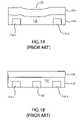
- an interlevel dielectric (ILD) layer 135 is formed over a metal level 130 .
- Metal level 130 includes patterned metal lines 110 (i.e., 110 - 1 , 110 - 2 ) separated by a dielectric 132 .
- chemical-mechanical polishing of the surface of interlevel dielectric layer 135 may result in an indentation 131 in regions between metal lines 110 .
- dummy metal patterns may be added to metal levels.
- the number of dummy metal patterns to be added to a metal level may depend on pattern density requirements.
- Dummy metal patterns which are also referred to as “waffles” or “dummy fill patterns,” allow the thickness of an interlevel dielectric to remain consistent during CMP.
- dummy metal patterns have no electrical function in the integrated circuit. That is, current is not flown through dummy metal patterns.
- a dummy metal pattern 120 is added between metal lines 110 . Dummy metal pattern 120 has no electrical function and is accordingly left electrically floating.
- Computer aided design programs may be employed to create a process model that describes the behavior of an integrated circuit.
- Process models allow designers to simulate the integrated circuit for testing, optimization, and other purposes.
- the dummy metal patterns may be added or drawn to the circuit layout just prior to tape out after the timing closure step is complete. Although there is no current flow through a dummy metal pattern, it may interact with other nets affecting the parasitic capacitance, which impacts circuit timing.
- Some pattern density simulation tools such as the ChampgeoTM software from UbiTech, Inc., accept process parameters and a layout to simulate for oxide variation across the die.
- the resulting process model is specific to particular layouts and must be derived every time the layout is changed.
- a level in a process technology for an integrated circuit that has dummy metal patterns is represented as a level in a process model.
- the level of the process model may comprise a high-k dielectric to represent the dummy metal patterns.
- each metal line may be surrounded by a normal dielectric. If the process technology has voids or pockets of air in between the metal lines, then each void or air pocket may be placed in a normal dielectric in the process model. Among other advantages, this allows the process model to take into account the effects of the dummy metal patterns.
- FIGS. 1A and 1B schematically illustrate the use of dummy metal patterns in integrated circuits.
- FIG. 2 shows a flow diagram of a method of creating a process model in accordance with an embodiment of the present invention.
- FIGS. 3A , 3 B, and 3 C schematically show levels of a process model in accordance with an embodiment of the present invention.
- FIG. 4A schematically shows a cross-section of a process technology for an integrated circuit.
- FIG. 4B schematically shows a process model for the process technology of FIG. 4A , in accordance with an embodiment of the present invention.
- FIG. 5 shows a flow diagram of a method of accounting for the effects of dummy metal patterns in integrated circuits, in accordance with an embodiment of the present invention.
- FIGS. 6A and 6B schematically illustrate void critical distance.
- Embodiments of the present invention may be employed in the design and manufacture of integrated circuits that have dummy metal patterns.
- an improved process model that takes into account the effects of dummy metal patterns is created. Details of this improved process model are further discussed beginning with FIG. 2 .
- the improved process model is then employed in conjunction with a high capacity or full chip capable parasitic extraction tool to characterize the interconnects of the integrated circuit. Examples of such extraction tools include the AssuraTM and QXTM software from Cadence Design systems and the CaliberTM software from Mentor Graphics.
- the extraction of parasitic capacitance is a complex problem and accurate extractions involve the use of 3D (three dimensional) field solvers. While accurate, 3D analysis is capacity limited. Even for relatively small 6 to 10 net circuits, extraction may take 10 to 20 hours to complete.
- High-capacity extraction tools use 3D field solver technology to calculate capacitance for different types of interconnect structures. These predetermined set of interconnect structures and their capacitance values are stored in a library format. This process is also referred to as interconnect characterization for a technology and is performed once per technology. For the AssuraTM software, a program called “capgen” performs this task; for the QXTM software, a program called “icecaps” performs this task, etc.
- the extraction process is reduced to recognition of interconnect structures in the circuit layout that match the predetermined set of interconnect structures in the library.
- a curve fitting mechanism is then employed to calculate the parasitic capacitance in the circuit layout.
- This interconnect characterization may be performed using the improved process model or its variants.
- the improved process model may be used for “capgen” when employing the AssuraTM software, for icecap when employing the QXTM software, and so on.
- FIG. 2 shows a flow diagram of a method 200 of creating a process model in accordance with an embodiment of the present invention.
- Method 200 will be described with reference to FIGS. 3A , 3 B, and 3 C, which schematically show levels that take into account the effects of dummy metal patterns in accordance with embodiments of the present invention.
- a level of a process technology for an integrated circuit that has dummy metal patterns is represented in a process model by a high-k dielectric layer.
- a process technology generally describes an integrated circuit in terms of the process to be used in fabricating the integrated circuit.
- a high-k dielectric layer may comprise a dielectric material having a dielectric constant equal to or greater than about 15. Silicon dioxide is the most commonly used dielectric material. The relative dielectric constant of silicon dioxide is about 3.0 to 4.0. It is to be noted that some emerging new dielectric materials have a relative dielectric constant less than about 3.0 (low-k).
- a high-k dielectric constant is any value above 10.0.
- An example model level with such a high-k dielectric layer is shown in FIG. 3A . In FIG.
- high-k dielectric layer 340 is so named because it has a relatively high dielectric constant.
- the dielectric constant of layer 340 depends on the particulars of the process technology. For example, the dielectric constant of layer 340 may be about 15 or greater.
- the dielectric constant assigned to layer 340 may be verified and optimized in a verification step, such as step 508 of the later discussed method 500 .
- each metal is surrounded by a “normal” dielectric in the process model.
- the normal dielectric is the dielectric surrounding the metal in the actual integrated circuit.
- the normal dielectric may be placed between the metals and the high-k dielectric layer.
- FIG. 3B An example model of a metal level in accordance with step 204 is shown in FIG. 3B .
- a metal 310 may be a patterned metal line in the actual integrated circuit.
- the metal 310 is also surrounded by a normal dielectric 330 , which comprises dielectric material present with the metal 310 . Space not occupied by the normal dielectric 330 and the metal 310 remains occupied by the high-k dielectric layer 340 .
- Dimensions D 370 - 1 and D 370 - 2 form the width of a normal dielectric 330 surrounding the metal 310 .
- the width of the normal dielectric 330 in the model may depend on the particulars of the process technology.
- each dimension D 370 i.e., D 370 - 1 or D 370 - 2
- metal level 130 shown in FIG. 1B may be modeled as shown in FIG. 3B , with dielectric 132 being represented by normal dielectric 330 , a metal 110 being represented by the metal 310 , and the rest of the regions in the model level being occupied by the high-k dielectric layer 340 .
- step 206 if voids are present in the actual integrated circuit, the voids are placed between metals in the process model. In one embodiment, the voids are represented in the model as regions within a normal dielectric.
- An example model level in accordance with step 206 is shown in FIG. 3C .
- the voids 317 i.e., 317 - 1 , 317 - 2
- the voids 317 are placed in the model level within normal dielectric 330 .
- the process model resulting from method 200 may be implemented using commercially available extraction tools, such as the previously mentioned software from Cadence Designs Systems and Mentor Graphics, for example.
- the process model advantageously takes into account the effects of dummy metal patterns without appreciably increasing parasitic capacitance extraction time.
- Method 200 may be employed in the design of both full-custom and “ASIC-like” integrated circuits without appreciably limiting the capacity of existing extraction tools.
- FIG. 4A schematically shows a cross-section of a process technology for an integrated circuit.
- the integrated circuit includes overlying levels 451 - 455 .
- Level 451 comprises dummy metal patterns 320 and dielectric 330 .
- Dielectric 330 may comprise any suitable interlevel dielectric (ILD) material, such as silicon dioxide.
- An interlevel dielectric may have a dielectric constant between about 3.0 to 4.0, for example.
- Level 452 which comprises a layer of dielectric 330 , is over level 451 .
- Level 453 comprises dummy metal patterns 320 , metals 310 , and dielectric 330 .
- Level 454 is the same as level 452
- level 455 is the same as level 451 .
- FIG. 4B schematically shows the new process model for the model of FIG. 4A .
- the model of FIG. 4B may be generated using method 200 , and may be employed for parasitic capacitance extraction.
- Levels 451 - 455 of the integrated circuit are represented in the process model by levels 461 - 465 , respectively.
- level 451 has dummy metal patterns 320 but does not include any metals. Accordingly, level 451 is represented in the new model by high-k dielectric layer 340 in level 461 (see step 202 of method 200 ). Level 452 does not include a metal or dummy metal pattern and is thus left the same in level 462 of the new model. Level 453 has metals 310 , dielectric 330 , and dummy metal patterns 320 . Accordingly, in level 463 of the model, metals 310 are surrounded by “normal” dielectric 330 , with the rest of level 463 being occupied by high-k dielectric layer 340 (see step 204 of method 200 ). Levels 454 and 455 are treated in the same way as levels 452 and 451 , respectively.
- step 502 the cross-section of the process technology for the integrated circuit to be modeled is obtained.
- the cross-section of the process technology may be based on electrical design rules, which dictate spacing between multiple levels of interconnect, the thickness of the metal lines, dielectrics, etc.
- the width of the normal dielectric surrounding each metal in the subsequently created process model is determined.
- the width of the normal dielectric depends on the particulars of the technology.
- the width of the normal dielectric in the model is based on the dimensions and spacing of the dummy metal patterns and the electrical design rules for the process technology.
- the dimensions and spacing of dummy metal patterns in the integrated circuit may be determined using techniques disclosed in U.S. Provisional Application No. 60/531,938, entitled “WAFFLING TECHNOLOGY BASED ON OXIDE PATTERN DENSITY,” filed on Dec. 23, 2003 by Walter Iandolo, Yitzhak Gilboa, and Artur Balasinski, which is incorporated herein by reference in its entirety.
- the width of the normal dielectric may be the larger of (a) twice the minimum allowable spacing between a dummy metal and a metal line or (b) twice the “void critical distance” when voids are present in the metal level. Twice the dimension is used in the embodiment because the width of a normal dielectric comprises two regions surrounding a metal line (e.g., see dimensions D 370 - 1 and D 370 - 2 for the metal 310 in FIG. 3B ).
- a dielectric 630 is deposited between metals 610 .
- Dielectric 630 may comprise a material that tends to form voids when deposited between narrowly spaced metal lines.
- a void 612 begins to form as the spacing between metals 610 is decreased. If the spacing between metals 610 is narrow enough, the void 612 will close as shown in FIG. 6B .
- the dimension D 600 between a metal 610 and the void 612 when the void 612 just closes is referred to as the void critical distance.
- the void critical distance may be used in determining the width of a normal dielectric in a process model.
- the process model is created.
- the process model may be based on the cross-section of the process technology obtained in step 502 and the width of the normal dielectric determined in step 504 .
- the process model is created using the method 200 previously discussed with reference to FIG. 2 .
- the resulting process model may be employed in conjunction with a parasitic capacitance extraction tool to characterize the interconnects of the integrated circuit.
- the process model is verified. In one embodiment, only a small portion of the process model is verified. For example, about 3 to 6 nets of the process model may be verified by simulating a test structure using a field solver tool, such as the RaphaelTM software from Synopsys, Inc.
- the cross-section of FIG. 4A is employed as a 3-wire test structure.
- the “3-wires” may be the metals 310 at level 453 .
- the dimensions, spacing, and other parameters of metals 310 , dummy metal patterns 320 , and dielectric 330 in the test structure may be obtained from the cross-section obtained from step 502 .
- FIG. 4B which is the resulting process model for the cross-section of FIG.
- the width of normal dielectric 330 in level 463 may be obtained from step 504 , while the dielectric constant of high-k dielectric layer 340 may be an expected value based on predictions or previous verification steps.
- the results of running a simulation using the process model of FIG. 4B may be compared to measured results of electrically testing the cross-section of FIG. 4A .
- the dielectric constant of high-k dielectric layer 340 and other parameters of the process model may be optimized until the results of the simulation agree with the results of the electrical testing.
- the dielectric constant of the high-k dielectric layer 340 may be changed until the measured capacitance of the center metal 310 (pointed to by arrow 342 in FIG. 4A ) of the test structure and the extracted capacitance of the center metal 310 in the process model (pointed to by arrow 352 in FIG. 4B ) agree to within 5%.
Abstract
Description
Claims (13)
Priority Applications (1)
| Application Number | Priority Date | Filing Date | Title |
|---|---|---|---|
| US10/876,396 US7254792B1 (en) | 2003-06-27 | 2004-06-25 | Accounting for the effects of dummy metal patterns in integrated circuits |
Applications Claiming Priority (2)
| Application Number | Priority Date | Filing Date | Title |
|---|---|---|---|
| US48346403P | 2003-06-27 | 2003-06-27 | |
| US10/876,396 US7254792B1 (en) | 2003-06-27 | 2004-06-25 | Accounting for the effects of dummy metal patterns in integrated circuits |
Publications (1)
| Publication Number | Publication Date |
|---|---|
| US7254792B1 true US7254792B1 (en) | 2007-08-07 |
Family
ID=38324474
Family Applications (1)
| Application Number | Title | Priority Date | Filing Date |
|---|---|---|---|
| US10/876,396 Expired - Fee Related US7254792B1 (en) | 2003-06-27 | 2004-06-25 | Accounting for the effects of dummy metal patterns in integrated circuits |
Country Status (1)
| Country | Link |
|---|---|
| US (1) | US7254792B1 (en) |
Cited By (6)
| Publication number | Priority date | Publication date | Assignee | Title |
|---|---|---|---|---|
| US20070298527A1 (en) * | 2006-06-23 | 2007-12-27 | Essam Mina | Determining geometrical configuration of interconnect structure |
| US20100077372A1 (en) * | 2008-09-25 | 2010-03-25 | International Business Machines Corporation | Apparatus, Method and Computer Program Product for Fast Stimulation of Manufacturing Effects During Integrated Circuit Design |
| US8464200B1 (en) | 2012-02-15 | 2013-06-11 | International Business Machines Corporation | Thermal relief optimization |
| US8566773B2 (en) * | 2012-02-15 | 2013-10-22 | International Business Machines Corporation | Thermal relief automation |
| US10223520B2 (en) | 2013-02-22 | 2019-03-05 | Duo Security, Inc. | System and method for integrating two-factor authentication in a device |
| US10345694B2 (en) * | 2014-08-25 | 2019-07-09 | Blobalfoundries Inc. | Model-based generation of dummy features |
Citations (11)
| Publication number | Priority date | Publication date | Assignee | Title |
|---|---|---|---|---|
| US5790417A (en) * | 1996-09-25 | 1998-08-04 | Taiwan Semiconductor Manufacturing Company Ltd. | Method of automatic dummy layout generation |
| US6037249A (en) * | 1997-12-31 | 2000-03-14 | Intel Corporation | Method for forming air gaps for advanced interconnect systems |
| US6243653B1 (en) * | 1998-08-17 | 2001-06-05 | Vlsi Technology, Inc. | Methods and apparatus for extracting parasitic capacitance values from a physical design of an integrated circuit |
| US6381730B1 (en) * | 1999-07-09 | 2002-04-30 | Sequence Design, Inc. | Method and system for extraction of parasitic interconnect impedance including inductance |
| US20020116686A1 (en) * | 2001-02-21 | 2002-08-22 | Shin Jae-Pil | Continuously variable dummy pattern density generating systems, methods and computer program products for patterning integrated circuits |
| US20020144224A1 (en) * | 2001-04-02 | 2002-10-03 | Martin Frerichs | Method for calculating the capacity of a layout of an integrated circuit with the aid of a computer, and application of the method to integrated circuit fabrication |
| US20030229875A1 (en) * | 2002-06-07 | 2003-12-11 | Smith Taber H. | Use of models in integrated circuit fabrication |
| US6678879B1 (en) * | 1999-06-02 | 2004-01-13 | Cypress Semiconductor Corp. | Method and apparatus for automated design of integrated circuits |
| US20040158805A1 (en) * | 2003-02-07 | 2004-08-12 | Renesas Technology Corp. | Parasitic capacitance extracting device and method for semiconductor integrated circuit |
| US6816999B2 (en) * | 2001-12-11 | 2004-11-09 | Samsung Electronics Co., Ltd. | Method of extracting interconnection capacitance of semiconductor integrated chip and recording medium for recording the same |
| US6854100B1 (en) * | 2002-08-27 | 2005-02-08 | Taiwan Semiconductor Manufacturing Company | Methodology to characterize metal sheet resistance of copper damascene process |
-
2004
- 2004-06-25 US US10/876,396 patent/US7254792B1/en not_active Expired - Fee Related
Patent Citations (11)
| Publication number | Priority date | Publication date | Assignee | Title |
|---|---|---|---|---|
| US5790417A (en) * | 1996-09-25 | 1998-08-04 | Taiwan Semiconductor Manufacturing Company Ltd. | Method of automatic dummy layout generation |
| US6037249A (en) * | 1997-12-31 | 2000-03-14 | Intel Corporation | Method for forming air gaps for advanced interconnect systems |
| US6243653B1 (en) * | 1998-08-17 | 2001-06-05 | Vlsi Technology, Inc. | Methods and apparatus for extracting parasitic capacitance values from a physical design of an integrated circuit |
| US6678879B1 (en) * | 1999-06-02 | 2004-01-13 | Cypress Semiconductor Corp. | Method and apparatus for automated design of integrated circuits |
| US6381730B1 (en) * | 1999-07-09 | 2002-04-30 | Sequence Design, Inc. | Method and system for extraction of parasitic interconnect impedance including inductance |
| US20020116686A1 (en) * | 2001-02-21 | 2002-08-22 | Shin Jae-Pil | Continuously variable dummy pattern density generating systems, methods and computer program products for patterning integrated circuits |
| US20020144224A1 (en) * | 2001-04-02 | 2002-10-03 | Martin Frerichs | Method for calculating the capacity of a layout of an integrated circuit with the aid of a computer, and application of the method to integrated circuit fabrication |
| US6816999B2 (en) * | 2001-12-11 | 2004-11-09 | Samsung Electronics Co., Ltd. | Method of extracting interconnection capacitance of semiconductor integrated chip and recording medium for recording the same |
| US20030229875A1 (en) * | 2002-06-07 | 2003-12-11 | Smith Taber H. | Use of models in integrated circuit fabrication |
| US6854100B1 (en) * | 2002-08-27 | 2005-02-08 | Taiwan Semiconductor Manufacturing Company | Methodology to characterize metal sheet resistance of copper damascene process |
| US20040158805A1 (en) * | 2003-02-07 | 2004-08-12 | Renesas Technology Corp. | Parasitic capacitance extracting device and method for semiconductor integrated circuit |
Cited By (8)
| Publication number | Priority date | Publication date | Assignee | Title |
|---|---|---|---|---|
| US20070298527A1 (en) * | 2006-06-23 | 2007-12-27 | Essam Mina | Determining geometrical configuration of interconnect structure |
| US7490304B2 (en) * | 2006-06-23 | 2009-02-10 | International Business Machines Corporation | Determining geometrical configuration of interconnect structure |
| US20100077372A1 (en) * | 2008-09-25 | 2010-03-25 | International Business Machines Corporation | Apparatus, Method and Computer Program Product for Fast Stimulation of Manufacturing Effects During Integrated Circuit Design |
| US8117568B2 (en) | 2008-09-25 | 2012-02-14 | International Business Machines Corporation | Apparatus, method and computer program product for fast simulation of manufacturing effects during integrated circuit design |
| US8464200B1 (en) | 2012-02-15 | 2013-06-11 | International Business Machines Corporation | Thermal relief optimization |
| US8566773B2 (en) * | 2012-02-15 | 2013-10-22 | International Business Machines Corporation | Thermal relief automation |
| US10223520B2 (en) | 2013-02-22 | 2019-03-05 | Duo Security, Inc. | System and method for integrating two-factor authentication in a device |
| US10345694B2 (en) * | 2014-08-25 | 2019-07-09 | Blobalfoundries Inc. | Model-based generation of dummy features |
Similar Documents
| Publication | Publication Date | Title |
|---|---|---|
| US6854100B1 (en) | Methodology to characterize metal sheet resistance of copper damascene process | |
| Mehrotra et al. | A methodology for modeling the effects of systematic within-die interconnect and device variation on circuit performance | |
| US8572537B2 (en) | Accurate parasitic capacitance extraction for ultra large scale integrated circuits | |
| US7363099B2 (en) | Integrated circuit metrology | |
| US7475377B2 (en) | Semiconductor device design system and method, and software product for the same | |
| US6243653B1 (en) | Methods and apparatus for extracting parasitic capacitance values from a physical design of an integrated circuit | |
| US8312406B2 (en) | Method and system performing RC extraction | |
| JP4846605B2 (en) | Timing verification method and timing verification apparatus | |
| KR100396900B1 (en) | Method for extracting interconnection capacitance of semiconductor integrated chip and recording media for recording the same | |
| Wong et al. | An empirical three-dimensional crossover capacitance model for multilevel interconnect VLSI circuits | |
| US7254792B1 (en) | Accounting for the effects of dummy metal patterns in integrated circuits | |
| US20070266360A1 (en) | Metal Thickness Simulation for Improving RC Extraction Accuracy | |
| US8495532B2 (en) | Systems and methods for creating frequency-dependent RC extraction netlist | |
| US8418112B2 (en) | Method of generating RC technology file | |
| TW200428238A (en) | Method of determining arrangement of wire in semiconductor integrated circuit | |
| US10013523B2 (en) | Full-chip assessment of time-dependent dielectric breakdown | |
| Qi et al. | Measurement and characterization of pattern dependent process variations of interconnect resistance, capacitance and inductance in nanometer technologies | |
| Kim et al. | Simple and accurate models for capacitance increment due to metal fill insertion | |
| US8667433B2 (en) | Polishing estimation/evaluation device, overpolishing condition calculation device, and computer-readable non-transitory medium thereof | |
| Rodriguez et al. | Hotspot prevention using CMP model in design implementation flow | |
| Oh et al. | Interconnect modeling for VLSIs | |
| Jung et al. | Interconnect modeling in deep-submicron design | |
| US20130196453A1 (en) | Presumably defective portion decision apparatus, presumably defective portion decision method, fabrication method for semiconductor device and program | |
| Katakamsetty et al. | Timing-aware metal fill for optimized timing impact and uniformity | |
| Oh et al. | Interconnect modeling in deep submicron design |
Legal Events
| Date | Code | Title | Description |
|---|---|---|---|
| AS | Assignment |
Owner name: CYPRESS SEMICONDUCTOR CORPORATION, CALIFORNIA Free format text: ASSIGNMENT OF ASSIGNORS INTEREST;ASSIGNORS:REKHI, SANJAY;LA BOUFF, MICHAEL;REEL/FRAME:015519/0527 Effective date: 20040624 |
|
| FEPP | Fee payment procedure |
Free format text: PAYER NUMBER DE-ASSIGNED (ORIGINAL EVENT CODE: RMPN); ENTITY STATUS OF PATENT OWNER: LARGE ENTITY Free format text: PAYOR NUMBER ASSIGNED (ORIGINAL EVENT CODE: ASPN); ENTITY STATUS OF PATENT OWNER: LARGE ENTITY |
|
| FPAY | Fee payment |
Year of fee payment: 4 |
|
| REMI | Maintenance fee reminder mailed | ||
| AS | Assignment |
Owner name: MORGAN STANLEY SENIOR FUNDING, INC., NEW YORK Free format text: SECURITY INTEREST;ASSIGNORS:CYPRESS SEMICONDUCTOR CORPORATION;SPANSION LLC;REEL/FRAME:035240/0429 Effective date: 20150312 |
|
| LAPS | Lapse for failure to pay maintenance fees | ||
| STCH | Information on status: patent discontinuation |
Free format text: PATENT EXPIRED DUE TO NONPAYMENT OF MAINTENANCE FEES UNDER 37 CFR 1.362 |
|
| FP | Lapsed due to failure to pay maintenance fee |
Effective date: 20150807 |
|
| AS | Assignment |
Owner name: MORGAN STANLEY SENIOR FUNDING, INC., NEW YORK Free format text: CORRECTIVE ASSIGNMENT TO CORRECT THE 8647899 PREVIOUSLY RECORDED ON REEL 035240 FRAME 0429. ASSIGNOR(S) HEREBY CONFIRMS THE SECURITY INTERST;ASSIGNORS:CYPRESS SEMICONDUCTOR CORPORATION;SPANSION LLC;REEL/FRAME:058002/0470 Effective date: 20150312 |