US7265415B2 - MOS-gated transistor with reduced miller capacitance - Google Patents
MOS-gated transistor with reduced miller capacitance Download PDFInfo
- Publication number
- US7265415B2 US7265415B2 US10/962,367 US96236704A US7265415B2 US 7265415 B2 US7265415 B2 US 7265415B2 US 96236704 A US96236704 A US 96236704A US 7265415 B2 US7265415 B2 US 7265415B2
- Authority
- US
- United States
- Prior art keywords
- region
- well region
- gate trench
- trench
- conductivity type
- Prior art date
- Legal status (The legal status is an assumption and is not a legal conclusion. Google has not performed a legal analysis and makes no representation as to the accuracy of the status listed.)
- Active
Links
- 239000000758 substrate Substances 0.000 claims description 26
- 229910021420 polycrystalline silicon Inorganic materials 0.000 claims description 11
- 229920005591 polysilicon Polymers 0.000 claims description 11
- 229910000577 Silicon-germanium Inorganic materials 0.000 claims description 10
- 239000000463 material Substances 0.000 claims description 6
- JMASRVWKEDWRBT-UHFFFAOYSA-N Gallium nitride Chemical compound [Ga]#N JMASRVWKEDWRBT-UHFFFAOYSA-N 0.000 claims description 5
- LEVVHYCKPQWKOP-UHFFFAOYSA-N [Si].[Ge] Chemical compound [Si].[Ge] LEVVHYCKPQWKOP-UHFFFAOYSA-N 0.000 claims description 5
- 229910021419 crystalline silicon Inorganic materials 0.000 claims description 5
- HBMJWWWQQXIZIP-UHFFFAOYSA-N silicon carbide Chemical compound [Si+]#[C-] HBMJWWWQQXIZIP-UHFFFAOYSA-N 0.000 claims description 5
- 239000002210 silicon-based material Substances 0.000 claims 30
- 239000007943 implant Substances 0.000 description 28
- XUIMIQQOPSSXEZ-UHFFFAOYSA-N Silicon Chemical compound [Si] XUIMIQQOPSSXEZ-UHFFFAOYSA-N 0.000 description 17
- 229910052710 silicon Inorganic materials 0.000 description 17
- 239000010703 silicon Substances 0.000 description 17
- 239000002019 doping agent Substances 0.000 description 16
- 238000000034 method Methods 0.000 description 6
- 230000000873 masking effect Effects 0.000 description 3
- 238000004088 simulation Methods 0.000 description 3
- 238000007796 conventional method Methods 0.000 description 2
- ZOXJGFHDIHLPTG-UHFFFAOYSA-N Boron Chemical compound [B] ZOXJGFHDIHLPTG-UHFFFAOYSA-N 0.000 description 1
- 230000002411 adverse Effects 0.000 description 1
- 230000000903 blocking effect Effects 0.000 description 1
- 229910052796 boron Inorganic materials 0.000 description 1
- 230000001413 cellular effect Effects 0.000 description 1
- 230000007423 decrease Effects 0.000 description 1
- 238000010586 diagram Methods 0.000 description 1
- 239000003989 dielectric material Substances 0.000 description 1
- 238000005530 etching Methods 0.000 description 1
- 230000003116 impacting effect Effects 0.000 description 1
- 238000004519 manufacturing process Methods 0.000 description 1
- 239000004065 semiconductor Substances 0.000 description 1
Images


Classifications
-
- H—ELECTRICITY
- H01—ELECTRIC ELEMENTS
- H01L—SEMICONDUCTOR DEVICES NOT COVERED BY CLASS H10
- H01L29/00—Semiconductor devices adapted for rectifying, amplifying, oscillating or switching, or capacitors or resistors with at least one potential-jump barrier or surface barrier, e.g. PN junction depletion layer or carrier concentration layer; Details of semiconductor bodies or of electrodes thereof ; Multistep manufacturing processes therefor
- H01L29/66—Types of semiconductor device ; Multistep manufacturing processes therefor
- H01L29/68—Types of semiconductor device ; Multistep manufacturing processes therefor controllable by only the electric current supplied, or only the electric potential applied, to an electrode which does not carry the current to be rectified, amplified or switched
- H01L29/76—Unipolar devices, e.g. field effect transistors
- H01L29/772—Field effect transistors
- H01L29/78—Field effect transistors with field effect produced by an insulated gate
- H01L29/7801—DMOS transistors, i.e. MISFETs with a channel accommodating body or base region adjoining a drain drift region
- H01L29/7802—Vertical DMOS transistors, i.e. VDMOS transistors
- H01L29/7813—Vertical DMOS transistors, i.e. VDMOS transistors with trench gate electrode, e.g. UMOS transistors
-
- H—ELECTRICITY
- H01—ELECTRIC ELEMENTS
- H01L—SEMICONDUCTOR DEVICES NOT COVERED BY CLASS H10
- H01L29/00—Semiconductor devices adapted for rectifying, amplifying, oscillating or switching, or capacitors or resistors with at least one potential-jump barrier or surface barrier, e.g. PN junction depletion layer or carrier concentration layer; Details of semiconductor bodies or of electrodes thereof ; Multistep manufacturing processes therefor
- H01L29/02—Semiconductor bodies ; Multistep manufacturing processes therefor
- H01L29/06—Semiconductor bodies ; Multistep manufacturing processes therefor characterised by their shape; characterised by the shapes, relative sizes, or dispositions of the semiconductor regions ; characterised by the concentration or distribution of impurities within semiconductor regions
- H01L29/0603—Semiconductor bodies ; Multistep manufacturing processes therefor characterised by their shape; characterised by the shapes, relative sizes, or dispositions of the semiconductor regions ; characterised by the concentration or distribution of impurities within semiconductor regions characterised by particular constructional design considerations, e.g. for preventing surface leakage, for controlling electric field concentration or for internal isolations regions
- H01L29/0607—Semiconductor bodies ; Multistep manufacturing processes therefor characterised by their shape; characterised by the shapes, relative sizes, or dispositions of the semiconductor regions ; characterised by the concentration or distribution of impurities within semiconductor regions characterised by particular constructional design considerations, e.g. for preventing surface leakage, for controlling electric field concentration or for internal isolations regions for preventing surface leakage or controlling electric field concentration
- H01L29/0611—Semiconductor bodies ; Multistep manufacturing processes therefor characterised by their shape; characterised by the shapes, relative sizes, or dispositions of the semiconductor regions ; characterised by the concentration or distribution of impurities within semiconductor regions characterised by particular constructional design considerations, e.g. for preventing surface leakage, for controlling electric field concentration or for internal isolations regions for preventing surface leakage or controlling electric field concentration for increasing or controlling the breakdown voltage of reverse biased devices
- H01L29/0615—Semiconductor bodies ; Multistep manufacturing processes therefor characterised by their shape; characterised by the shapes, relative sizes, or dispositions of the semiconductor regions ; characterised by the concentration or distribution of impurities within semiconductor regions characterised by particular constructional design considerations, e.g. for preventing surface leakage, for controlling electric field concentration or for internal isolations regions for preventing surface leakage or controlling electric field concentration for increasing or controlling the breakdown voltage of reverse biased devices by the doping profile or the shape or the arrangement of the PN junction, or with supplementary regions, e.g. junction termination extension [JTE]
- H01L29/0619—Semiconductor bodies ; Multistep manufacturing processes therefor characterised by their shape; characterised by the shapes, relative sizes, or dispositions of the semiconductor regions ; characterised by the concentration or distribution of impurities within semiconductor regions characterised by particular constructional design considerations, e.g. for preventing surface leakage, for controlling electric field concentration or for internal isolations regions for preventing surface leakage or controlling electric field concentration for increasing or controlling the breakdown voltage of reverse biased devices by the doping profile or the shape or the arrangement of the PN junction, or with supplementary regions, e.g. junction termination extension [JTE] with a supplementary region doped oppositely to or in rectifying contact with the semiconductor containing or contacting region, e.g. guard rings with PN or Schottky junction
- H01L29/0623—Buried supplementary region, e.g. buried guard ring
-
- H—ELECTRICITY
- H01—ELECTRIC ELEMENTS
- H01L—SEMICONDUCTOR DEVICES NOT COVERED BY CLASS H10
- H01L29/00—Semiconductor devices adapted for rectifying, amplifying, oscillating or switching, or capacitors or resistors with at least one potential-jump barrier or surface barrier, e.g. PN junction depletion layer or carrier concentration layer; Details of semiconductor bodies or of electrodes thereof ; Multistep manufacturing processes therefor
- H01L29/02—Semiconductor bodies ; Multistep manufacturing processes therefor
- H01L29/06—Semiconductor bodies ; Multistep manufacturing processes therefor characterised by their shape; characterised by the shapes, relative sizes, or dispositions of the semiconductor regions ; characterised by the concentration or distribution of impurities within semiconductor regions
- H01L29/0684—Semiconductor bodies ; Multistep manufacturing processes therefor characterised by their shape; characterised by the shapes, relative sizes, or dispositions of the semiconductor regions ; characterised by the concentration or distribution of impurities within semiconductor regions characterised by the shape, relative sizes or dispositions of the semiconductor regions or junctions between the regions
- H01L29/0692—Surface layout
- H01L29/0696—Surface layout of cellular field-effect devices, e.g. multicellular DMOS transistors or IGBTs
-
- H—ELECTRICITY
- H01—ELECTRIC ELEMENTS
- H01L—SEMICONDUCTOR DEVICES NOT COVERED BY CLASS H10
- H01L29/00—Semiconductor devices adapted for rectifying, amplifying, oscillating or switching, or capacitors or resistors with at least one potential-jump barrier or surface barrier, e.g. PN junction depletion layer or carrier concentration layer; Details of semiconductor bodies or of electrodes thereof ; Multistep manufacturing processes therefor
- H01L29/02—Semiconductor bodies ; Multistep manufacturing processes therefor
- H01L29/06—Semiconductor bodies ; Multistep manufacturing processes therefor characterised by their shape; characterised by the shapes, relative sizes, or dispositions of the semiconductor regions ; characterised by the concentration or distribution of impurities within semiconductor regions
- H01L29/10—Semiconductor bodies ; Multistep manufacturing processes therefor characterised by their shape; characterised by the shapes, relative sizes, or dispositions of the semiconductor regions ; characterised by the concentration or distribution of impurities within semiconductor regions with semiconductor regions connected to an electrode not carrying current to be rectified, amplified or switched and such electrode being part of a semiconductor device which comprises three or more electrodes
- H01L29/1095—Body region, i.e. base region, of DMOS transistors or IGBTs
-
- H—ELECTRICITY
- H01—ELECTRIC ELEMENTS
- H01L—SEMICONDUCTOR DEVICES NOT COVERED BY CLASS H10
- H01L29/00—Semiconductor devices adapted for rectifying, amplifying, oscillating or switching, or capacitors or resistors with at least one potential-jump barrier or surface barrier, e.g. PN junction depletion layer or carrier concentration layer; Details of semiconductor bodies or of electrodes thereof ; Multistep manufacturing processes therefor
- H01L29/66—Types of semiconductor device ; Multistep manufacturing processes therefor
- H01L29/66007—Multistep manufacturing processes
- H01L29/66075—Multistep manufacturing processes of devices having semiconductor bodies comprising group 14 or group 13/15 materials
- H01L29/66227—Multistep manufacturing processes of devices having semiconductor bodies comprising group 14 or group 13/15 materials the devices being controllable only by the electric current supplied or the electric potential applied, to an electrode which does not carry the current to be rectified, amplified or switched, e.g. three-terminal devices
- H01L29/66409—Unipolar field-effect transistors
- H01L29/66477—Unipolar field-effect transistors with an insulated gate, i.e. MISFET
- H01L29/66674—DMOS transistors, i.e. MISFETs with a channel accommodating body or base region adjoining a drain drift region
- H01L29/66712—Vertical DMOS transistors, i.e. VDMOS transistors
- H01L29/66734—Vertical DMOS transistors, i.e. VDMOS transistors with a step of recessing the gate electrode, e.g. to form a trench gate electrode
-
- H—ELECTRICITY
- H01—ELECTRIC ELEMENTS
- H01L—SEMICONDUCTOR DEVICES NOT COVERED BY CLASS H10
- H01L29/00—Semiconductor devices adapted for rectifying, amplifying, oscillating or switching, or capacitors or resistors with at least one potential-jump barrier or surface barrier, e.g. PN junction depletion layer or carrier concentration layer; Details of semiconductor bodies or of electrodes thereof ; Multistep manufacturing processes therefor
- H01L29/66—Types of semiconductor device ; Multistep manufacturing processes therefor
- H01L29/68—Types of semiconductor device ; Multistep manufacturing processes therefor controllable by only the electric current supplied, or only the electric potential applied, to an electrode which does not carry the current to be rectified, amplified or switched
- H01L29/76—Unipolar devices, e.g. field effect transistors
- H01L29/772—Field effect transistors
- H01L29/78—Field effect transistors with field effect produced by an insulated gate
- H01L29/7831—Field effect transistors with field effect produced by an insulated gate with multiple gate structure
Definitions
- This invention relates in general to semiconductor power devices and in particular to a trench MOS-gated transistor with reduced miller capacitance.
- FIG. 1 shows a simplified cross-section view of a conventional vertical trenched gate MOSFET 100 .
- An epitaxial layer 104 of n-type conductivity type extends over n-type substrate 102 which forms the drain contact region.
- Well region 106 of p-type conductivity type is formed in an upper portion of epitaxial layer 104 .
- Gate trench 109 extends through well region 106 and terminates just below the interface between epitaxial layer 104 and well region 106 .
- Gate trench 109 is lined with a dielectric layer 112 along its sidewalls and bottom, and is filled with polysilicon material 110 forming the transistor gate.
- Source regions 108 flank each side of trench 109 , and overlap gate 110 along the vertical dimension. In the on-state, a current flows vertically from drain terminal 114 to source terminal 116 through substrate 102 , epitaxial layer 104 , channel regions in well region 106 along the outer sidewalls of trench 109 , and finally source regions 108 .
- Epitaxial layer 104 together with substrate 102 form the drain region.
- gate 110 overlaps the drain region along the bottom of trench 109 . It is desirable to minimize this gate-drain overlap in order to improve the transistor switching speed.
- the gate-drain charge Qgd is proportional to this overlap area and inversely proportional to the thickness of the dielectric along the bottom of trench 109 .
- Several methods to reduce Qgd have been proposed including reducing the trench width, using thicker dielectric along the trench bottom, eliminating portions of the gate along the trench flat bottom portion, and extending the p-type well region slightly deeper than the trench. Each of these techniques has its own advantages and disadvantages. Some require a more complex process technology, while others are not as effective in reducing Qgd without adversely impacting other device characteristics.
- an MOS-gated transistor with improved characteristics including a substantially reduced miller capacitance, and which is simple to manufacture is desirable.
- a trench MOS-gated transistor includes a first region of a first conductivity type forming a pn junction with a well region of a second conductivity type.
- the well region has a flat bottom portion and a portion extending deeper than the flat bottom portion.
- a gate trench extends into the well region. Channel regions extend in the well region along outer sidewalls of the gate trench.
- the gate trench has a first bottom portion which terminates within the first region and a second portion which terminates within the deeper portion of the well region such that when the transistor is in an on state the deeper portion of the well region prevents a current from flowing through those channel region portions located directly above the deeper portion of the well region.
- a trench MOS-gated transistor includes a silicon layer of a first conductivity type over a silicon substrate.
- a well region of a second conductivity type is formed in an upper portion of the silicon layer.
- a gate trench extends through the well region and terminates within the silicon layer. Source regions of the first conductivity type flank each side of the gate trench.
- the gate trench is filled with a polysilicon material at least up to and partially overlapping with the source regions.
- a silicon region of the second conductivity type extends along a bottom portion of the trench such that a gap is formed between the silicon region and the well region through which gap a current flows when the transistor is in an on state.
- a trench MOS-gated transistor is formed as follows. A first region of a first conductivity type is provided. A well region of a second conductivity type is then formed in an upper portion of the first region. A trench is formed which extends through the well region and terminates within the first region. Dopants of the second conductivity type are implanted along predefined portions of the bottom of the trench to form regions along the bottom of the trench which are contiguous with the well region such that when the transistor is in an on state the deeper portion of the well region prevents a current from flowing through those channel region portions located directly above the deeper portion of the well region.
- a trench MOS-gated transistor is formed as follows. An epitaxial layer of a first conductivity type is formed over a substrate. A well region of a second conductivity type is formed in an upper portion of the epitaxial layer. A trench is formed which extends through the well region and terminates within the epitaxial layer. Dopants of the second conductivity type are implanted along the bottom of the trench to form a region of the second conductivity type extending along a bottom portion of the trench such that a gap is formed between the region of the second conductivity type and the well region through which gap a current flows when the transistor is in an on state.
- FIG. 1 shows a simplified cross-section view of a conventional vertical trenched gate MOSFET
- FIG. 2A shows a simplified cross section view of a vertical trenched-gate MOSFET in accordance with an embodiment of the present invention
- FIG. 2B shows a simplified top layout view of the vertical trenched-gate MOSFET in FIG. 2A ;
- FIG. 3 shows a simplified cross section view of a vertical trenched-gate MOSFET in accordance with another embodiment of the present invention.
- FIG. 4 shows a simplified top layout view of an alternate embodiment of the present invention wherein the cell structures in FIGS. 2A and 3 are combined;
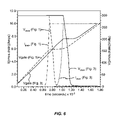
- FIG. 5 shows the current and voltage waveforms for the FIG. 2A MOSFET embodiment versus those for the prior art FIG. 1 MOSFET;
- FIG. 6 shows current and voltage waveforms for the FIG. 3 MOSFET versus those for the prior art FIG. 1 MOSFET.
- the gate-drain capacitance of a MOSFET is reduced by using an implant region under the trenched gate wherein the implant region is contiguous with the well region of the MOSFET.
- the implant region makes the area of the trench under which it is formed inactive as it blocks conduction in the corresponding portion of the transistor channel.
- One suitable application for this embodiment would be high voltage devices in which the contribution of the channel resistance to the transistor on resistance Rdson is low.
- an implant region under the gate trench is formed such that there is a gap between the implant region and the well region through which the channel current can flow. In this embodiment, the impact of the implant region on Rdson is minimized, and thus a suitable application for this embodiment would be low voltage devices.
- Both these embodiments are particularly useful in designs requiring a tight trench cell pitch such as tight alternating pn pillar pitch of a superjunction device or low Rdson. These two embodiments may be combined together in a single MOSFET. Alternatively, one of both of these embodiments may be combined with the prior art structure shown in FIG. 1 as needed.
- FIG. 2A shows a simplified cross section view of a vertical trenched-gate MOSFET 200 in accordance with an embodiment of the present invention.
- An epitaxial layer 204 of n-type conductivity type extends over n-type substrate 202 which forms the drain contact region.
- Well region 206 of p-type conductivity type is formed in an upper portion of epitaxial layer 204 .
- Gate trench 209 extends through well region 206 .
- a portion 206 a of well region 206 directly below trench 209 extends deeper into epitaxial layer 204 than other portions of well region 206 such that gate trench 209 terminates within portion 206 a .
- Gate trench 209 is lined with a dielectric layer 212 along its sidewalls and bottom.
- Trench 209 is filled with polysilicon material 210 forming the transistor gate. Source regions 208 flank each side of trench 209 and overlap gate 210 along the vertical dimension. In an alternate embodiment, trench 209 is partially filled with polysilicon material with dielectric material atop the polysilicon. Note that one or more of substrate 202 , epitaxial layer 204 , well region 206 including portion 206 a , and source regions 208 may be from crystalline silicon (Si), silicon carbide (SiC), gallium nitride (GaN), or silicon germanium (SiGe).
- the trenched-gate cell is stripe shape (i.e., is laid out in an open cell configuration) as shown in the simplified top layout view in FIG. 2B .
- Stripe-shaped trenched-gate 210 extends vertically with source regions 208 flanking each side of trenched-gate electrode 210 .
- deeper extending well portions 206 a are formed periodically along a length of the striped trenched-gate electrode 210 .
- portion 206 a is not formed (e.g., along dashed line 1 - 1 ) the cell cross section is similar to that in FIG.
- gate trench 210 extends clear through well region 206 and terminates within epitaxial layer 204 such the gate trench overlaps epitaxial layer 204 along the vertical dimension.
- current flow is established (in a similar manner to that described above in reference to FIG. 1 ) along those portions of the trench sidewalls below which deeper extending well portions 206 a are not formed.
- Current flow is however blocked where deeper extending well portions 206 a are formed under the gate.
- the gate-drain overlap is thus reduced by an amount corresponding to portions 206 a .
- the gate to source capacitance or Qgs increases.
- the Qgd/Qgs ratio advantageously decreases further. The switching characteristics of the MOSFET are therefore substantially improved.
- the FIG. 2A structure is formed as follows.
- Epitaxial layer 204 is formed over substrate 202 using conventional techniques.
- Well region 206 is formed in an upper portion of epitaxial layer 204 by implanting and driving in p-type dopants using known techniques.
- Trench 209 is then formed by etching the silicon using conventional silicon etch techniques. Using a masking layer, the bottom of trench 209 is then selectively implanted with p-type dopants to thus form regions 206 a .
- an implant dose in the range of 1 ⁇ 10 13 -1 ⁇ 10 14 cm ⁇ 3 and an implant energy in the range of 40-120 KeV are used.
- the thickness of region 206 a at its deepest point is in the range of 0.2-0.41 ⁇ m.
- Dielectric layer 212 , doped polysilicon 2210 filling trench 209 , and source regions 208 are all formed using conventional methods.
- FIG. 3 shows a simplified cross section view of a vertical trenched-gate MOSFET 300 in accordance with another embodiment of the present invention.
- Cross section view of MOSFET 300 is similar to that in FIG. 2A except that instead of the deeper extending well portion 206 a , p-type region 307 is formed directly below trench 309 .
- region 307 is formed such that there is a gap between well region 306 and region 307 at each of the bottom corners of trench 309 . During the on state, current flows through these gaps. Thus, by using region 307 with gaps as shown, the gate-drain overlap is significantly reduced without blocking the current flow.
- region 307 is formed by carrying out a shallow boron implant through the bottom the trench using an implant energy in the range of 30-80 KeV. In one embodiment, region 307 has a thickness in the range of 0.1-0.3 ⁇ m, and the gap between region 307 and well region 306 is in the range of 0.1-0.3 ⁇ m.
- substrate 302 , epitaxial layer 304 , well region 306 , region 307 , and source regions 308 may be from crystalline silicon (Si), silicon carbide (SiC), gallium nitride (GaN), or silicon germanium (SiGe).
- region 307 may be continuous along the length of the striped trench gate. Region 307 may be extended up at the ends of or other locations along the striped trench gate to electrically contact well region 306 . Alternatively, region 307 is not biased and thus is allowed to electrically float. In an alternate embodiment, similar to the layout shown in FIG. 2B , a number of p-type regions 307 are formed periodically along the length of the stripe such that the cell structure along portions of the stripe (e.g., at dashed line 1 - 1 ) is similar to that in prior art FIG. 1 . Alternatively, the FIG. 2A and FIG. 3 embodiments may be combined as shown in the layout diagram in FIG. 4 . In FIG.
- regions 206 a correspond to region 206 a in FIG. 2A and regions 307 correspond to region 307 in FIG. 3 .
- no current conduction occurs where regions 206 a are formed, but current can flow where regions 307 are formed as well as between regions 206 a and 307 .
- the particular arrangement of regions 307 and 206 a is not limited to that shown in FIG. 4 . Many other arrangements are possible.
- the regions between regions 206 a and 307 are eliminated such that nowhere along the stripe is a cell structure similar to that shown in the prior art FIG. 1 is formed.
- the well region 206 and region 206 a under the gate trench in FIG. 2A , and the well region 306 and the region 307 under the gate trench in FIG. 3 may be formed as follows.
- a shallow blanket implant (in the active region) of p-type dopants into the epitaxial layer is carried out.
- a deep implant of p-type dopants into selected areas of the epitaxial layer is then carried out using a masking layer. These two implant steps may be carried out in reverse order.
- a temperature cycle is then carried out to drive both implanted dopants deeper into the epitaxial layer.
- a well region corresponding to the shallow blanket implant and predefined silicon regions corresponding to the deep implant are formed in the epitaxial layer such that the deepest portion of the predefined silicon regions is deeper than a bottom surface of the well region.
- the above two implant steps and the temperature cycle need to be designed so that after driving in the dopants, the silicon regions are contiguous with the well regions.
- the two implant steps and the temperature cycle need to be designed so that after the dopants are driven in and the gate trench is formed, a gap is formed between each of the silicon regions and the well region.
- one skilled in the art would know how to design the two implant steps and the temperature cycle in order to obtain the structures shown in FIGS. 2A and 3 .
- a shallow implant of p-type dopants into selected areas of the epitaxial layer is first carried out using a masking layer.
- a temperature cycle is then performed to drive the implanted dopants deeper into the epitaxial layer.
- a blanket implant (in the active region) of p-type dopants into the first silicon region is then carried out.
- a second temperature cycle is then performed to drive the implanted dopants from the blanket implant step deeper into the epitaxial layer and to drive the dopants from the shallow implant step even deeper into the epitaxial layer.
- a well region corresponding to the blanket implant and silicon regions corresponding to the shallow implant are formed such that the deepest portion of the silicon regions is deeper than a bottom surface of the well region.
- the above two implant steps and two temperature cycles need to be designed so that after driving in the dopants the silicon regions are contiguous with the well regions.
- the two implant steps and the two implant steps need to be designed so that after the dopants are driven in and the gate trench is formed, a gap is formed between each of the silicon regions and the well region.
- one skilled in the art would know how to design the two the implant steps and the two temperature cycles in order to obtain the structures shown in FIGS. 2A and 3 .
- the table below shows the simulation results for Qgs, Qgd, and Qgd/Qgs ratio for each of MOSFET 100 in prior art FIG. 1 , MOSFET 200 in FIG. 2A , and MOSFET 300 in FIG. 3 .
- a 600V superjunction MOSFET with a 6 ⁇ m pitch and 0.6 ⁇ m trench width was used for the simulation.
- FIG. 1 FIG. 2A
- FIG. 3 Qgs nC/cm 2 72.8 103.8 73.2
- Qgd nC/cm 2 36.4 27.3 31.6 Qgd/Qgs 0.50 0.26 0.43
- MOSFETS 200 and 300 both have lower Qgd than prior art MOSFET 100 , and both have higher Qgs than prior art MOSFET 100 .
- a lower Qgd/Qgs ratio is thus obtained for both MOSFETs 200 and 300 than that for MOSFET 100 .
- the simulation waveforms in FIGS. 5 and 6 show similar results.
- FIG. 5 shows the Idrain, Vdrain, and Vgate for the FIG. 2A MOSFET and for the prior art FIG. 1 MOSFET
- FIG. 6 shows the same parameters for the FIG. 3 MOSFET and the prior art FIG. 1 MOSFET.
- the cross-section views and top layout view of the different embodiments may not be to scale, and as such are not intended to limit the possible variations in the layout design of the corresponding structures.
- the various transistors can be formed in cellular architecture including hexagonal or square shaped transistor cells.
- embodiments of the invention are not limited thereto.
- the doping polarities of the structures shown and described could be reversed and/or the doping concentrations of the various elements could be altered without departing from the invention.
- the various exemplary vertical transistors described above have the trenches terminating in the drift regions, but they can also terminate in the more heavily doped substrate.
- the present invention is shown and described in the context of vertical MOSFET embodiments, but regions 206 a in FIG. 2A and 307 in FIG. 3 can be similarly formed in other trenched gate structures such as trenched gate IGBTs and lateral trenched gate MOSFETs.
Abstract
Description
| Parameter | FIG. 1 | FIG. 2A | FIG. 3 | ||
| Qgs nC/cm2 | 72.8 | 103.8 | 73.2 | ||
| Qgd nC/cm2 | 36.4 | 27.3 | 31.6 | ||
| Qgd/Qgs | 0.50 | 0.26 | 0.43 | ||
Claims (23)
Priority Applications (10)
| Application Number | Priority Date | Filing Date | Title |
|---|---|---|---|
| US10/962,367 US7265415B2 (en) | 2004-10-08 | 2004-10-08 | MOS-gated transistor with reduced miller capacitance |
| KR1020097010188A KR100929714B1 (en) | 2004-10-08 | 2005-10-04 | Mos-gated transistor with reduced miller capacitance |
| PCT/US2005/035620 WO2006041823A2 (en) | 2004-10-08 | 2005-10-04 | Mos-gated transistor with reduced miller capacitance |
| EP05802949.7A EP1803159B1 (en) | 2004-10-08 | 2005-10-04 | Mos-gated transistor with reduced miller capacitance |
| JP2007535749A JP2008516451A (en) | 2004-10-08 | 2005-10-04 | MOS gate structure transistor with low mirror capacitance |
| CN2005800343157A CN101091258B (en) | 2004-10-08 | 2005-10-04 | Mos-gated transistor with reduced miller capacitance |
| TW094135172A TWI393254B (en) | 2004-10-08 | 2005-10-07 | Mos-gated transistor with reducde milleer capacitance |
| KR1020077010389A KR100919528B1 (en) | 2004-10-08 | 2007-05-07 | Mos-gated transistor with reduced miller capacitance and method of forming the same |
| US11/829,262 US7534683B2 (en) | 2004-10-08 | 2007-07-27 | Method of making a MOS-gated transistor with reduced miller capacitance |
| HK08106795.6A HK1112111A1 (en) | 2004-10-08 | 2008-06-19 | Mos-gated transistor with reduced miller capacitance |
Applications Claiming Priority (1)
| Application Number | Priority Date | Filing Date | Title |
|---|---|---|---|
| US10/962,367 US7265415B2 (en) | 2004-10-08 | 2004-10-08 | MOS-gated transistor with reduced miller capacitance |
Related Child Applications (1)
| Application Number | Title | Priority Date | Filing Date |
|---|---|---|---|
| US11/829,262 Division US7534683B2 (en) | 2004-10-08 | 2007-07-27 | Method of making a MOS-gated transistor with reduced miller capacitance |
Publications (2)
| Publication Number | Publication Date |
|---|---|
| US20060076617A1 US20060076617A1 (en) | 2006-04-13 |
| US7265415B2 true US7265415B2 (en) | 2007-09-04 |
Family
ID=36144410
Family Applications (2)
| Application Number | Title | Priority Date | Filing Date |
|---|---|---|---|
| US10/962,367 Active US7265415B2 (en) | 2004-10-08 | 2004-10-08 | MOS-gated transistor with reduced miller capacitance |
| US11/829,262 Expired - Fee Related US7534683B2 (en) | 2004-10-08 | 2007-07-27 | Method of making a MOS-gated transistor with reduced miller capacitance |
Family Applications After (1)
| Application Number | Title | Priority Date | Filing Date |
|---|---|---|---|
| US11/829,262 Expired - Fee Related US7534683B2 (en) | 2004-10-08 | 2007-07-27 | Method of making a MOS-gated transistor with reduced miller capacitance |
Country Status (8)
| Country | Link |
|---|---|
| US (2) | US7265415B2 (en) |
| EP (1) | EP1803159B1 (en) |
| JP (1) | JP2008516451A (en) |
| KR (2) | KR100929714B1 (en) |
| CN (1) | CN101091258B (en) |
| HK (1) | HK1112111A1 (en) |
| TW (1) | TWI393254B (en) |
| WO (1) | WO2006041823A2 (en) |
Cited By (10)
| Publication number | Priority date | Publication date | Assignee | Title |
|---|---|---|---|---|
| US20060267082A1 (en) * | 2005-05-31 | 2006-11-30 | Franz Hofmann | Semiconductor memory component |
| US20080088340A1 (en) * | 2006-10-16 | 2008-04-17 | Freescale Semiconductor, Inc. | Miller capacitance tolerant buffer element |
| US20080135927A1 (en) * | 2006-11-22 | 2008-06-12 | Fuji Electric Device Technology Co., Ltd. | Semiconductor device and manufacturing method thereof |
| US20090114949A1 (en) * | 2007-11-01 | 2009-05-07 | Alpha & Omega Semiconductor, Ltd. | High-mobility trench mosfets |
| US7534683B2 (en) * | 2004-10-08 | 2009-05-19 | Fairchild Semiconductor Corporation | Method of making a MOS-gated transistor with reduced miller capacitance |
| US20090273026A1 (en) * | 2002-10-03 | 2009-11-05 | Wilson Peter H | Trench-gate ldmos structures |
| US8785278B2 (en) | 2012-02-02 | 2014-07-22 | Alpha And Omega Semiconductor Incorporated | Nano MOSFET with trench bottom oxide shielded and third dimensional P-body contact |
| US10367091B2 (en) * | 2016-02-26 | 2019-07-30 | Toyota Jidosha Kabushiki Kaisha | Semiconductor switching element |
| US10374081B2 (en) * | 2016-02-26 | 2019-08-06 | Toyota Jidosha Kabushiki Kaisha | Semiconductor switching element |
| DE102018106670A1 (en) * | 2018-03-21 | 2019-09-26 | Infineon Technologies Ag | A silicon carbide semiconductor device having a trench gate structure and a source region in an upper region of a mesa section |
Families Citing this family (38)
| Publication number | Priority date | Publication date | Assignee | Title |
|---|---|---|---|---|
| JP4644730B2 (en) * | 2008-08-12 | 2011-03-02 | 株式会社日立製作所 | Semiconductor device and power conversion device using the same |
| US8237195B2 (en) * | 2008-09-29 | 2012-08-07 | Fairchild Semiconductor Corporation | Power MOSFET having a strained channel in a semiconductor heterostructure on metal substrate |
| CN101807546B (en) * | 2009-02-13 | 2013-04-17 | 尼克森微电子股份有限公司 | Trench type metal-oxide semiconductor device and manufacture method thereof |
| US8242510B2 (en) * | 2010-01-28 | 2012-08-14 | Intersil Americas Inc. | Monolithic integration of gallium nitride and silicon devices and circuits, structure and method |
| US8525260B2 (en) * | 2010-03-19 | 2013-09-03 | Monolithic Power Systems, Inc. | Super junction device with deep trench and implant |
| US8304828B2 (en) * | 2010-03-22 | 2012-11-06 | Great Power Semiconductor Corp. | Closed cell trench power MOSFET structure |
| JP5531787B2 (en) * | 2010-05-31 | 2014-06-25 | 株式会社デンソー | Silicon carbide semiconductor device and manufacturing method thereof |
| US8313995B2 (en) | 2011-01-13 | 2012-11-20 | Infineon Technologies Austria Ag | Method for manufacturing a semiconductor device |
| JP5717661B2 (en) * | 2011-03-10 | 2015-05-13 | 株式会社東芝 | Semiconductor device and manufacturing method thereof |
| CN102184960B (en) * | 2011-04-22 | 2016-07-27 | 上海华虹宏力半导体制造有限公司 | Power MOSFET pipe and forming method thereof |
| EP3151285B1 (en) | 2011-09-08 | 2023-11-22 | Tamura Corporation | Ga2o3-based semiconductor element |
| EP2765610B1 (en) * | 2011-09-08 | 2018-12-26 | Tamura Corporation | Ga2o3 semiconductor element |
| EP2602829A1 (en) | 2011-12-07 | 2013-06-12 | Nxp B.V. | Trench-gate resurf semiconductor device and manufacturing method |
| TW201421683A (en) * | 2012-11-23 | 2014-06-01 | Anpec Electronics Corp | Semiconductor device with reduced miller capacitance and fabrication method thereof |
| TWI544635B (en) | 2014-03-20 | 2016-08-01 | 帥群微電子股份有限公司 | Trench power mosfet and manufacturing method thereof |
| US9443973B2 (en) * | 2014-11-26 | 2016-09-13 | Infineon Technologies Austria Ag | Semiconductor device with charge compensation region underneath gate trench |
| DE102014117780B4 (en) | 2014-12-03 | 2018-06-21 | Infineon Technologies Ag | Semiconductor device with a trench electrode and method of manufacture |
| DE102014119465B3 (en) * | 2014-12-22 | 2016-05-25 | Infineon Technologies Ag | SEMICONDUCTOR DEVICE WITH STRIPULAR TRENCHGATE STRUCTURES, TRANSISTORMESIS AND DIODE MESAS |
| JP2017112161A (en) * | 2015-12-15 | 2017-06-22 | 三菱電機株式会社 | Semiconductor device |
| US10032907B2 (en) * | 2016-10-04 | 2018-07-24 | Nexperia B.V. | TrenchMOS |
| US9887287B1 (en) * | 2016-12-08 | 2018-02-06 | Cree, Inc. | Power semiconductor devices having gate trenches with implanted sidewalls and related methods |
| CN106449419A (en) * | 2016-12-08 | 2017-02-22 | 西安电子科技大学 | Ga2O3-material-based U-shaped grating type MOSFET and preparation method thereof |
| WO2018225600A1 (en) * | 2017-06-06 | 2018-12-13 | 三菱電機株式会社 | Semiconductor device and power conversion apparatus |
| CN109427886A (en) * | 2017-08-25 | 2019-03-05 | 比亚迪股份有限公司 | MOSFET and preparation method, electronic equipment, vehicle |
| CN109671766B (en) * | 2017-10-13 | 2023-06-27 | 联华电子股份有限公司 | Power mosfet |
| JP2019087611A (en) * | 2017-11-06 | 2019-06-06 | トヨタ自動車株式会社 | Switching element and manufacturing method thereof |
| DE102018103973B4 (en) | 2018-02-22 | 2020-12-03 | Infineon Technologies Ag | SILICON CARBIDE SEMICONDUCTOR COMPONENT |
| DE102019111308A1 (en) | 2018-05-07 | 2019-11-07 | Infineon Technologies Ag | SILICON CARBIDE SEMICONDUCTOR ELEMENT |
| CN109037337A (en) * | 2018-06-28 | 2018-12-18 | 华为技术有限公司 | A kind of power semiconductor and manufacturing method |
| JP7005453B2 (en) * | 2018-08-08 | 2022-01-21 | 株式会社東芝 | Semiconductor device |
| DE102018124740A1 (en) | 2018-10-08 | 2020-04-09 | Infineon Technologies Ag | SEMICONDUCTOR COMPONENT WITH A SIC SEMICONDUCTOR BODY AND METHOD FOR PRODUCING A SEMICONDUCTOR COMPONENT |
| US10903322B2 (en) | 2018-11-16 | 2021-01-26 | Infineon Technologies Ag | SiC power semiconductor device with integrated body diode |
| US10586845B1 (en) | 2018-11-16 | 2020-03-10 | Infineon Technologies Ag | SiC trench transistor device and methods of manufacturing thereof |
| US10985248B2 (en) | 2018-11-16 | 2021-04-20 | Infineon Technologies Ag | SiC power semiconductor device with integrated Schottky junction |
| CN110137259A (en) * | 2019-04-11 | 2019-08-16 | 深圳大学 | MOSFET pipe and preparation method thereof |
| CN111584365B (en) * | 2020-04-29 | 2024-01-30 | 北京时代民芯科技有限公司 | Manufacturing method of low miller capacitance trench gate VDMOS device |
| WO2022104074A1 (en) * | 2020-11-13 | 2022-05-19 | The Regents Of The University Of California | Epitaxy-enabled substrate transfer |
| CN117393585B (en) * | 2023-12-07 | 2024-04-05 | 深圳市冠禹半导体有限公司 | MOSFET device with high driving capability and driving circuit thereof |
Citations (99)
| Publication number | Priority date | Publication date | Assignee | Title |
|---|---|---|---|---|
| US3404295A (en) | 1964-11-30 | 1968-10-01 | Motorola Inc | High frequency and voltage transistor with added region for punch-through protection |
| US3412297A (en) | 1965-12-16 | 1968-11-19 | United Aircraft Corp | Mos field-effect transistor with a onemicron vertical channel |
| US3497777A (en) | 1967-06-13 | 1970-02-24 | Stanislas Teszner | Multichannel field-effect semi-conductor device |
| US3564356A (en) | 1968-10-24 | 1971-02-16 | Tektronix Inc | High voltage integrated circuit transistor |
| US3660697A (en) | 1970-02-16 | 1972-05-02 | Bell Telephone Labor Inc | Monolithic semiconductor apparatus adapted for sequential charge transfer |
| US4003072A (en) | 1972-04-20 | 1977-01-11 | Sony Corporation | Semiconductor device with high voltage breakdown resistance |
| US4011105A (en) | 1975-09-15 | 1977-03-08 | Mos Technology, Inc. | Field inversion control for n-channel device integrated circuits |
| US4300150A (en) | 1980-06-16 | 1981-11-10 | North American Philips Corporation | Lateral double-diffused MOS transistor device |
| US4324038A (en) | 1980-11-24 | 1982-04-13 | Bell Telephone Laboratories, Incorporated | Method of fabricating MOS field effect transistors |
| US4326332A (en) | 1980-07-28 | 1982-04-27 | International Business Machines Corp. | Method of making a high density V-MOS memory array |
| US4337474A (en) | 1978-08-31 | 1982-06-29 | Mitsubishi Denki Kabushiki Kaisha | Semiconductor device |
| US4345265A (en) | 1980-04-14 | 1982-08-17 | Supertex, Inc. | MOS Power transistor with improved high-voltage capability |
| US4445202A (en) | 1980-11-12 | 1984-04-24 | International Business Machines Corporation | Electrically switchable permanent storage |
| US4568958A (en) | 1984-01-03 | 1986-02-04 | General Electric Company | Inversion-mode insulated-gate gallium arsenide field-effect transistors |
| US4579621A (en) | 1983-07-08 | 1986-04-01 | Mitsubishi Denki Kabushiki Kaisha | Selective epitaxial growth method |
| US4636281A (en) | 1984-06-14 | 1987-01-13 | Commissariat A L'energie Atomique | Process for the autopositioning of a local field oxide with respect to an insulating trench |
| US4638344A (en) | 1979-10-09 | 1987-01-20 | Cardwell Jr Walter T | Junction field-effect transistor controlled by merged depletion regions |
| US4639761A (en) | 1983-12-16 | 1987-01-27 | North American Philips Corporation | Combined bipolar-field effect transistor resurf devices |
| US4673962A (en) | 1985-03-21 | 1987-06-16 | Texas Instruments Incorporated | Vertical DRAM cell and method |
| US4698653A (en) | 1979-10-09 | 1987-10-06 | Cardwell Jr Walter T | Semiconductor devices controlled by depletion regions |
| US4716126A (en) | 1986-06-05 | 1987-12-29 | Siliconix Incorporated | Fabrication of double diffused metal oxide semiconductor transistor |
| US4745079A (en) | 1987-03-30 | 1988-05-17 | Motorola, Inc. | Method for fabricating MOS transistors having gates with different work functions |
| US4746630A (en) | 1986-09-17 | 1988-05-24 | Hewlett-Packard Company | Method for producing recessed field oxide with improved sidewall characteristics |
| US4754310A (en) | 1980-12-10 | 1988-06-28 | U.S. Philips Corp. | High voltage semiconductor device |
| US4767722A (en) | 1986-03-24 | 1988-08-30 | Siliconix Incorporated | Method for making planar vertical channel DMOS structures |
| US4774556A (en) | 1985-07-25 | 1988-09-27 | Nippondenso Co., Ltd. | Non-volatile semiconductor memory device |
| US4801986A (en) | 1987-04-03 | 1989-01-31 | General Electric Company | Vertical double diffused metal oxide semiconductor VDMOS device with increased safe operating area and method |
| US4821095A (en) | 1987-03-12 | 1989-04-11 | General Electric Company | Insulated gate semiconductor device with extra short grid and method of fabrication |
| US4823176A (en) | 1987-04-03 | 1989-04-18 | General Electric Company | Vertical double diffused metal oxide semiconductor (VDMOS) device including high voltage junction exhibiting increased safe operating area |
| US4824793A (en) | 1984-09-27 | 1989-04-25 | Texas Instruments Incorporated | Method of making DRAM cell with trench capacitor |
| US4853345A (en) | 1988-08-22 | 1989-08-01 | Delco Electronics Corporation | Process for manufacture of a vertical DMOS transistor |
| US4868624A (en) | 1980-05-09 | 1989-09-19 | Regents Of The University Of Minnesota | Channel collector transistor |
| US4893160A (en) | 1987-11-13 | 1990-01-09 | Siliconix Incorporated | Method for increasing the performance of trenched devices and the resulting structure |
| US4914058A (en) | 1987-12-29 | 1990-04-03 | Siliconix Incorporated | Grooved DMOS process with varying gate dielectric thickness |
| US4941026A (en) | 1986-12-05 | 1990-07-10 | General Electric Company | Semiconductor devices exhibiting minimum on-resistance |
| US4961100A (en) | 1988-06-20 | 1990-10-02 | General Electric Company | Bidirectional field effect semiconductor device and circuit |
| US4967245A (en) | 1988-03-14 | 1990-10-30 | Siliconix Incorporated | Trench power MOSFET device |
| US4969028A (en) | 1980-12-02 | 1990-11-06 | General Electric Company | Gate enhanced rectifier |
| US4974059A (en) | 1982-12-21 | 1990-11-27 | International Rectifier Corporation | Semiconductor high-power mosfet device |
| US4990463A (en) | 1988-07-05 | 1991-02-05 | Kabushiki Kaisha Toshiba | Method of manufacturing capacitor |
| US4992390A (en) | 1989-07-06 | 1991-02-12 | General Electric Company | Trench gate structure with thick bottom oxide |
| US5027180A (en) | 1986-12-11 | 1991-06-25 | Mitsubishi Electric Corporation | Double gate static induction thyristor |
| US5034785A (en) | 1986-03-24 | 1991-07-23 | Siliconix Incorporated | Planar vertical channel DMOS structure |
| US5065273A (en) | 1990-12-04 | 1991-11-12 | International Business Machines Corporation | High capacity DRAM trench capacitor and methods of fabricating same |
| US5072266A (en) | 1988-12-27 | 1991-12-10 | Siliconix Incorporated | Trench DMOS power transistor with field-shaping body profile and three-dimensional geometry |
| US5071782A (en) | 1990-06-28 | 1991-12-10 | Texas Instruments Incorporated | Vertical memory cell array and method of fabrication |
| US5079608A (en) | 1990-11-06 | 1992-01-07 | Harris Corporation | Power MOSFET transistor circuit with active clamp |
| US5105243A (en) | 1987-02-26 | 1992-04-14 | Kabushiki Kaisha Toshiba | Conductivity-modulation metal oxide field effect transistor with single gate structure |
| US5111253A (en) | 1989-05-09 | 1992-05-05 | General Electric Company | Multicellular FET having a Schottky diode merged therewith |
| US5134448A (en) | 1990-01-29 | 1992-07-28 | Motorola, Inc. | MOSFET with substrate source contact |
| US5142640A (en) | 1988-06-02 | 1992-08-25 | Seiko Epson Corporation | Trench gate metal oxide semiconductor field effect transistor |
| US5156989A (en) | 1988-11-08 | 1992-10-20 | Siliconix, Incorporated | Complementary, isolated DMOS IC technology |
| US5164802A (en) | 1991-03-20 | 1992-11-17 | Harris Corporation | Power vdmosfet with schottky on lightly doped drain of lateral driver fet |
| US5164325A (en) | 1987-10-08 | 1992-11-17 | Siliconix Incorporated | Method of making a vertical current flow field effect transistor |
| US5168331A (en) | 1991-01-31 | 1992-12-01 | Siliconix Incorporated | Power metal-oxide-semiconductor field effect transistor |
| US5168973A (en) | 1987-03-25 | 1992-12-08 | Kabushiki Kaisha Komatsu Seisakusho | Apparatus for controlling hydraulic pressure for clutch |
| US5188973A (en) | 1991-05-09 | 1993-02-23 | Nippon Telegraph & Telephone Corporation | Method of manufacturing SOI semiconductor element |
| US5208657A (en) | 1984-08-31 | 1993-05-04 | Texas Instruments Incorporated | DRAM Cell with trench capacitor and vertical channel in substrate |
| US5216275A (en) | 1991-03-19 | 1993-06-01 | University Of Electronic Science And Technology Of China | Semiconductor power devices with alternating conductivity type high-voltage breakdown regions |
| US5219777A (en) | 1991-06-14 | 1993-06-15 | Gold Star Electron Co., Ltd. | Metal oxide semiconductor field effect transistor and method of making the same |
| US5219793A (en) | 1991-06-03 | 1993-06-15 | Motorola Inc. | Method for forming pitch independent contacts and a semiconductor device having the same |
| US5233215A (en) | 1992-06-08 | 1993-08-03 | North Carolina State University At Raleigh | Silicon carbide power MOSFET with floating field ring and floating field plate |
| US5242845A (en) | 1990-06-13 | 1993-09-07 | Kabushiki Kaisha Toshiba | Method of production of vertical MOS transistor |
| US5250450A (en) | 1991-04-08 | 1993-10-05 | Micron Technology, Inc. | Insulated-gate vertical field-effect transistor with high current drive and minimum overlap capacitance |
| US5262336A (en) | 1986-03-21 | 1993-11-16 | Advanced Power Technology, Inc. | IGBT process to produce platinum lifetime control |
| US5268311A (en) | 1988-09-01 | 1993-12-07 | International Business Machines Corporation | Method for forming a thin dielectric layer on a substrate |
| US5275965A (en) | 1992-11-25 | 1994-01-04 | Micron Semiconductor, Inc. | Trench isolation using gated sidewalls |
| US5275961A (en) | 1990-11-23 | 1994-01-04 | Texas Instruments Incorporated | Method of forming insulated gate field-effect transistors |
| US5281548A (en) | 1992-07-28 | 1994-01-25 | Micron Technology, Inc. | Plug-based floating gate memory |
| US5294824A (en) | 1992-07-31 | 1994-03-15 | Motorola, Inc. | High voltage transistor having reduced on-resistance |
| US5300452A (en) | 1991-12-18 | 1994-04-05 | U.S. Philips Corporation | Method of manufacturing an optoelectronic semiconductor device |
| US5300447A (en) | 1992-09-29 | 1994-04-05 | Texas Instruments Incorporated | Method of manufacturing a minimum scaled transistor |
| US5326711A (en) | 1993-01-04 | 1994-07-05 | Texas Instruments Incorporated | High performance high voltage vertical transistor and method of fabrication |
| US5346834A (en) | 1988-11-21 | 1994-09-13 | Hitachi, Ltd. | Method for manufacturing a semiconductor device and a semiconductor memory device |
| US5350937A (en) | 1991-10-08 | 1994-09-27 | Semiconductor Energy Laboratory Co., Ltd. | Non-volatile memory device having a floating gate |
| US5365102A (en) | 1993-07-06 | 1994-11-15 | North Carolina State University | Schottky barrier rectifier with MOS trench |
| US5366914A (en) | 1992-01-29 | 1994-11-22 | Nec Corporation | Vertical power MOSFET structure having reduced cell area |
| US5389815A (en) | 1992-04-28 | 1995-02-14 | Mitsubishi Denki Kabushiki Kaisha | Semiconductor diode with reduced recovery current |
| US5405794A (en) | 1994-06-14 | 1995-04-11 | Philips Electronics North America Corporation | Method of producing VDMOS device of increased power density |
| US5418376A (en) | 1993-03-02 | 1995-05-23 | Toyo Denki Seizo Kabushiki Kaisha | Static induction semiconductor device with a distributed main electrode structure and static induction semiconductor device with a static induction main electrode shorted structure |
| US5424231A (en) | 1994-08-09 | 1995-06-13 | United Microelectronics Corp. | Method for manufacturing a VDMOS transistor |
| US5430311A (en) | 1991-09-20 | 1995-07-04 | Hitachi, Ltd. | Constant-voltage diode for over-voltage protection |
| US5430324A (en) | 1992-07-23 | 1995-07-04 | Siliconix, Incorporated | High voltage transistor having edge termination utilizing trench technology |
| US5429977A (en) | 1994-03-11 | 1995-07-04 | Industrial Technology Research Institute | Method for forming a vertical transistor with a stacked capacitor DRAM cell |
| US5434435A (en) | 1994-05-04 | 1995-07-18 | North Carolina State University | Trench gate lateral MOSFET |
| US5436189A (en) | 1989-10-03 | 1995-07-25 | Harris Corporation | Self-aligned channel stop for trench-isolated island |
| US5438215A (en) | 1993-03-25 | 1995-08-01 | Siemens Aktiengesellschaft | Power MOSFET |
| US5438007A (en) | 1993-07-02 | 1995-08-01 | Thunderbird Technologies, Inc. | Method of fabricating field effect transistor having polycrystalline silicon gate junction |
| US5473176A (en) | 1993-09-01 | 1995-12-05 | Kabushiki Kaisha Toshiba | Vertical insulated gate transistor and method of manufacture |
| US5473180A (en) | 1993-07-12 | 1995-12-05 | U.S. Philips Corporation | Semiconductor device with an MOST provided with an extended drain region for high voltages |
| US5474943A (en) | 1993-03-15 | 1995-12-12 | Siliconix Incorporated | Method for fabricating a short channel trenched DMOS transistor |
| US5488010A (en) | 1991-02-08 | 1996-01-30 | International Business Machines Corporation | Method of fabricating sidewall charge-coupled device with trench isolation |
| US5519245A (en) | 1989-08-31 | 1996-05-21 | Nippondenso Co., Ltd. | Insulated gate bipolar transistor with reverse conducting current |
| US5541425A (en) | 1994-01-20 | 1996-07-30 | Mitsubishi Denki Kabushiki Kaisha | Semiconductor device having trench structure |
| US5554552A (en) | 1995-04-03 | 1996-09-10 | Taiwan Semiconductor Manufacturing Company | PN junction floating gate EEPROM, flash EPROM device and method of manufacture thereof |
| US5554862A (en) | 1992-03-31 | 1996-09-10 | Kabushiki Kaisha Toshiba | Power semiconductor device |
| US5567634A (en) | 1995-05-01 | 1996-10-22 | National Semiconductor Corporation | Method of fabricating self-aligned contact trench DMOS transistors |
| US20030209741A1 (en) * | 2002-04-26 | 2003-11-13 | Wataru Saitoh | Insulated gate semiconductor device |
| US6930352B2 (en) * | 2003-04-07 | 2005-08-16 | Kabushiki Kaisha Toshiba | Insulated gate semiconductor device |
Family Cites Families (75)
| Publication number | Priority date | Publication date | Assignee | Title |
|---|---|---|---|---|
| US5298761A (en) * | 1991-06-17 | 1994-03-29 | Nikon Corporation | Method and apparatus for exposure process |
| US5597795A (en) * | 1992-10-27 | 1997-01-28 | The Procter & Gamble Company | Detergent compositions inhibiting dye transfer |
| KR960012585B1 (en) * | 1993-06-25 | 1996-09-23 | Samsung Electronics Co Ltd | Transistor structure and the method for manufacturing the same |
| DE4417150C2 (en) * | 1994-05-17 | 1996-03-14 | Siemens Ag | Method for producing an arrangement with self-reinforcing dynamic MOS transistor memory cells |
| US5583368A (en) * | 1994-08-11 | 1996-12-10 | International Business Machines Corporation | Stacked devices |
| US5674766A (en) * | 1994-12-30 | 1997-10-07 | Siliconix Incorporated | Method of making a trench MOSFET with multi-resistivity drain to provide low on-resistance by varying dopant concentration in epitaxial layer |
| US5597765A (en) * | 1995-01-10 | 1997-01-28 | Siliconix Incorporated | Method for making termination structure for power MOSFET |
| JP3325736B2 (en) * | 1995-02-09 | 2002-09-17 | 三菱電機株式会社 | Insulated gate semiconductor device |
| JP3291957B2 (en) * | 1995-02-17 | 2002-06-17 | 富士電機株式会社 | Vertical trench MISFET and method of manufacturing the same |
| US5595927A (en) * | 1995-03-17 | 1997-01-21 | Taiwan Semiconductor Manufacturing Company Ltd. | Method for making self-aligned source/drain mask ROM memory cell using trench etched channel |
| US5592005A (en) * | 1995-03-31 | 1997-01-07 | Siliconix Incorporated | Punch-through field effect transistor |
| US5744372A (en) * | 1995-04-12 | 1998-04-28 | National Semiconductor Corporation | Fabrication of complementary field-effect transistors each having multi-part channel |
| JPH08306914A (en) * | 1995-04-27 | 1996-11-22 | Nippondenso Co Ltd | Semiconductor device and its manufacture |
| US6049108A (en) * | 1995-06-02 | 2000-04-11 | Siliconix Incorporated | Trench-gated MOSFET with bidirectional voltage clamping |
| US5879971A (en) * | 1995-09-28 | 1999-03-09 | Motorola Inc. | Trench random access memory cell and method of formation |
| US5705409A (en) * | 1995-09-28 | 1998-01-06 | Motorola Inc. | Method for forming trench transistor structure |
| US5616945A (en) * | 1995-10-13 | 1997-04-01 | Siliconix Incorporated | Multiple gated MOSFET for use in DC-DC converter |
| US6037632A (en) * | 1995-11-06 | 2000-03-14 | Kabushiki Kaisha Toshiba | Semiconductor device |
| EP0879481B1 (en) * | 1996-02-05 | 2002-05-02 | Infineon Technologies AG | Field effect controlled semiconductor component |
| US5895951A (en) * | 1996-04-05 | 1999-04-20 | Megamos Corporation | MOSFET structure and fabrication process implemented by forming deep and narrow doping regions through doping trenches |
| US5719409A (en) * | 1996-06-06 | 1998-02-17 | Cree Research, Inc. | Silicon carbide metal-insulator semiconductor field effect transistor |
| JP2891205B2 (en) * | 1996-10-21 | 1999-05-17 | 日本電気株式会社 | Manufacturing method of semiconductor integrated circuit |
| US6168983B1 (en) * | 1996-11-05 | 2001-01-02 | Power Integrations, Inc. | Method of making a high-voltage transistor with multiple lateral conduction layers |
| US6207994B1 (en) * | 1996-11-05 | 2001-03-27 | Power Integrations, Inc. | High-voltage transistor with multi-layer conduction region |
| US6011298A (en) * | 1996-12-31 | 2000-01-04 | Stmicroelectronics, Inc. | High voltage termination with buried field-shaping region |
| KR100218260B1 (en) * | 1997-01-14 | 1999-09-01 | 김덕중 | Trench type mos transistor fabricating method |
| JP3938964B2 (en) * | 1997-02-10 | 2007-06-27 | 三菱電機株式会社 | High voltage semiconductor device and manufacturing method thereof |
| US5877528A (en) * | 1997-03-03 | 1999-03-02 | Megamos Corporation | Structure to provide effective channel-stop in termination areas for trenched power transistors |
| KR100225409B1 (en) * | 1997-03-27 | 1999-10-15 | 김덕중 | Trench dmos and method of manufacturing the same |
| US5879994A (en) * | 1997-04-15 | 1999-03-09 | National Semiconductor Corporation | Self-aligned method of fabricating terrace gate DMOS transistor |
| US6037628A (en) * | 1997-06-30 | 2000-03-14 | Intersil Corporation | Semiconductor structures with trench contacts |
| JP3502531B2 (en) * | 1997-08-28 | 2004-03-02 | 株式会社ルネサステクノロジ | Method for manufacturing semiconductor device |
| DE19740195C2 (en) * | 1997-09-12 | 1999-12-02 | Siemens Ag | Semiconductor device with metal-semiconductor junction with low reverse current |
| US6337499B1 (en) * | 1997-11-03 | 2002-01-08 | Infineon Technologies Ag | Semiconductor component |
| US5949104A (en) * | 1998-02-07 | 1999-09-07 | Xemod, Inc. | Source connection structure for lateral RF MOS devices |
| US5897343A (en) * | 1998-03-30 | 1999-04-27 | Motorola, Inc. | Method of making a power switching trench MOSFET having aligned source regions |
| US5945724A (en) * | 1998-04-09 | 1999-08-31 | Micron Technology, Inc. | Trench isolation region for semiconductor device |
| CN1166002C (en) * | 1998-04-23 | 2004-09-08 | 国际整流器有限公司 | P-shape channelled metal-oxide semiconductor FET transistor structure |
| US6048772A (en) * | 1998-05-04 | 2000-04-11 | Xemod, Inc. | Method for fabricating a lateral RF MOS device with an non-diffusion source-backside connection |
| DE19820223C1 (en) * | 1998-05-06 | 1999-11-04 | Siemens Ag | Variable doping epitaxial layer manufacturing method |
| US6015727A (en) * | 1998-06-08 | 2000-01-18 | Wanlass; Frank M. | Damascene formation of borderless contact MOS transistors |
| DE19848828C2 (en) * | 1998-10-22 | 2001-09-13 | Infineon Technologies Ag | Semiconductor device with low forward voltage and high blocking capability |
| US6194741B1 (en) * | 1998-11-03 | 2001-02-27 | International Rectifier Corp. | MOSgated trench type power semiconductor with silicon carbide substrate and increased gate breakdown voltage and reduced on-resistance |
| DE19854915C2 (en) * | 1998-11-27 | 2002-09-05 | Infineon Technologies Ag | MOS field effect transistor with auxiliary electrode |
| US6222229B1 (en) * | 1999-02-18 | 2001-04-24 | Cree, Inc. | Self-aligned shield structure for realizing high frequency power MOSFET devices with improved reliability |
| US6351018B1 (en) * | 1999-02-26 | 2002-02-26 | Fairchild Semiconductor Corporation | Monolithically integrated trench MOSFET and Schottky diode |
| US6204097B1 (en) * | 1999-03-01 | 2001-03-20 | Semiconductor Components Industries, Llc | Semiconductor device and method of manufacture |
| US6188105B1 (en) * | 1999-04-01 | 2001-02-13 | Intersil Corporation | High density MOS-gated power device and process for forming same |
| US6198127B1 (en) * | 1999-05-19 | 2001-03-06 | Intersil Corporation | MOS-gated power device having extended trench and doping zone and process for forming same |
| US6191447B1 (en) * | 1999-05-28 | 2001-02-20 | Micro-Ohm Corporation | Power semiconductor devices that utilize tapered trench-based insulating regions to improve electric field profiles in highly doped drift region mesas and methods of forming same |
| JP3851744B2 (en) * | 1999-06-28 | 2006-11-29 | 株式会社東芝 | Manufacturing method of semiconductor device |
| GB9917099D0 (en) * | 1999-07-22 | 1999-09-22 | Koninkl Philips Electronics Nv | Cellular trench-gate field-effect transistors |
| JP3971062B2 (en) * | 1999-07-29 | 2007-09-05 | 株式会社東芝 | High voltage semiconductor device |
| US20030060013A1 (en) * | 1999-09-24 | 2003-03-27 | Bruce D. Marchant | Method of manufacturing trench field effect transistors with trenched heavy body |
| US6222233B1 (en) * | 1999-10-04 | 2001-04-24 | Xemod, Inc. | Lateral RF MOS device with improved drain structure |
| US6461918B1 (en) * | 1999-12-20 | 2002-10-08 | Fairchild Semiconductor Corporation | Power MOS device with improved gate charge performance |
| US6346469B1 (en) * | 2000-01-03 | 2002-02-12 | Motorola, Inc. | Semiconductor device and a process for forming the semiconductor device |
| US6580123B2 (en) | 2000-04-04 | 2003-06-17 | International Rectifier Corporation | Low voltage power MOSFET device and process for its manufacture |
| US6627949B2 (en) * | 2000-06-02 | 2003-09-30 | General Semiconductor, Inc. | High voltage power MOSFET having low on-resistance |
| US6479352B2 (en) * | 2000-06-02 | 2002-11-12 | General Semiconductor, Inc. | Method of fabricating high voltage power MOSFET having low on-resistance |
| JP4528460B2 (en) * | 2000-06-30 | 2010-08-18 | 株式会社東芝 | Semiconductor element |
| US6534828B1 (en) * | 2000-09-19 | 2003-03-18 | Fairchild Semiconductor Corporation | Integrated circuit device including a deep well region and associated methods |
| US6362112B1 (en) * | 2000-11-08 | 2002-03-26 | Fabtech, Inc. | Single step etched moat |
| US7345342B2 (en) * | 2001-01-30 | 2008-03-18 | Fairchild Semiconductor Corporation | Power semiconductor devices and methods of manufacture |
| US6870220B2 (en) * | 2002-08-23 | 2005-03-22 | Fairchild Semiconductor Corporation | Method and apparatus for improved MOS gating to reduce miller capacitance and switching losses |
| US6677641B2 (en) * | 2001-10-17 | 2004-01-13 | Fairchild Semiconductor Corporation | Semiconductor structure with improved smaller forward voltage loss and higher blocking capability |
| US6683346B2 (en) * | 2001-03-09 | 2004-01-27 | Fairchild Semiconductor Corporation | Ultra dense trench-gated power-device with the reduced drain-source feedback capacitance and Miller charge |
| TWI248136B (en) * | 2002-03-19 | 2006-01-21 | Infineon Technologies Ag | Method for fabricating a transistor arrangement having trench transistor cells having a field electrode |
| JP3930436B2 (en) * | 2002-03-26 | 2007-06-13 | 株式会社東芝 | Semiconductor device |
| JP3935042B2 (en) * | 2002-04-26 | 2007-06-20 | 株式会社東芝 | Insulated gate semiconductor device |
| JP4028333B2 (en) * | 2002-09-02 | 2007-12-26 | 株式会社東芝 | Semiconductor device |
| DE10324754B4 (en) * | 2003-05-30 | 2018-11-08 | Infineon Technologies Ag | Semiconductor device |
| US7279743B2 (en) * | 2003-12-02 | 2007-10-09 | Vishay-Siliconix | Closed cell trench metal-oxide-semiconductor field effect transistor |
| GB0403934D0 (en) * | 2004-02-21 | 2004-03-24 | Koninkl Philips Electronics Nv | Trench-gate semiconductor devices and the manufacture thereof |
| US7265415B2 (en) * | 2004-10-08 | 2007-09-04 | Fairchild Semiconductor Corporation | MOS-gated transistor with reduced miller capacitance |
-
2004
- 2004-10-08 US US10/962,367 patent/US7265415B2/en active Active
-
2005
- 2005-10-04 JP JP2007535749A patent/JP2008516451A/en active Pending
- 2005-10-04 CN CN2005800343157A patent/CN101091258B/en not_active Expired - Fee Related
- 2005-10-04 KR KR1020097010188A patent/KR100929714B1/en active IP Right Grant
- 2005-10-04 EP EP05802949.7A patent/EP1803159B1/en not_active Expired - Fee Related
- 2005-10-04 WO PCT/US2005/035620 patent/WO2006041823A2/en active Application Filing
- 2005-10-07 TW TW094135172A patent/TWI393254B/en active
-
2007
- 2007-05-07 KR KR1020077010389A patent/KR100919528B1/en active IP Right Grant
- 2007-07-27 US US11/829,262 patent/US7534683B2/en not_active Expired - Fee Related
-
2008
- 2008-06-19 HK HK08106795.6A patent/HK1112111A1/en not_active IP Right Cessation
Patent Citations (101)
| Publication number | Priority date | Publication date | Assignee | Title |
|---|---|---|---|---|
| US3404295A (en) | 1964-11-30 | 1968-10-01 | Motorola Inc | High frequency and voltage transistor with added region for punch-through protection |
| US3412297A (en) | 1965-12-16 | 1968-11-19 | United Aircraft Corp | Mos field-effect transistor with a onemicron vertical channel |
| US3497777A (en) | 1967-06-13 | 1970-02-24 | Stanislas Teszner | Multichannel field-effect semi-conductor device |
| US3564356A (en) | 1968-10-24 | 1971-02-16 | Tektronix Inc | High voltage integrated circuit transistor |
| US3660697A (en) | 1970-02-16 | 1972-05-02 | Bell Telephone Labor Inc | Monolithic semiconductor apparatus adapted for sequential charge transfer |
| US4003072A (en) | 1972-04-20 | 1977-01-11 | Sony Corporation | Semiconductor device with high voltage breakdown resistance |
| US4011105A (en) | 1975-09-15 | 1977-03-08 | Mos Technology, Inc. | Field inversion control for n-channel device integrated circuits |
| US4337474A (en) | 1978-08-31 | 1982-06-29 | Mitsubishi Denki Kabushiki Kaisha | Semiconductor device |
| US4638344A (en) | 1979-10-09 | 1987-01-20 | Cardwell Jr Walter T | Junction field-effect transistor controlled by merged depletion regions |
| US4698653A (en) | 1979-10-09 | 1987-10-06 | Cardwell Jr Walter T | Semiconductor devices controlled by depletion regions |
| US4345265A (en) | 1980-04-14 | 1982-08-17 | Supertex, Inc. | MOS Power transistor with improved high-voltage capability |
| US4868624A (en) | 1980-05-09 | 1989-09-19 | Regents Of The University Of Minnesota | Channel collector transistor |
| US4300150A (en) | 1980-06-16 | 1981-11-10 | North American Philips Corporation | Lateral double-diffused MOS transistor device |
| US4326332A (en) | 1980-07-28 | 1982-04-27 | International Business Machines Corp. | Method of making a high density V-MOS memory array |
| US4445202A (en) | 1980-11-12 | 1984-04-24 | International Business Machines Corporation | Electrically switchable permanent storage |
| US4324038A (en) | 1980-11-24 | 1982-04-13 | Bell Telephone Laboratories, Incorporated | Method of fabricating MOS field effect transistors |
| US4969028A (en) | 1980-12-02 | 1990-11-06 | General Electric Company | Gate enhanced rectifier |
| US4754310A (en) | 1980-12-10 | 1988-06-28 | U.S. Philips Corp. | High voltage semiconductor device |
| US4974059A (en) | 1982-12-21 | 1990-11-27 | International Rectifier Corporation | Semiconductor high-power mosfet device |
| US4579621A (en) | 1983-07-08 | 1986-04-01 | Mitsubishi Denki Kabushiki Kaisha | Selective epitaxial growth method |
| US4639761A (en) | 1983-12-16 | 1987-01-27 | North American Philips Corporation | Combined bipolar-field effect transistor resurf devices |
| US4568958A (en) | 1984-01-03 | 1986-02-04 | General Electric Company | Inversion-mode insulated-gate gallium arsenide field-effect transistors |
| US4636281A (en) | 1984-06-14 | 1987-01-13 | Commissariat A L'energie Atomique | Process for the autopositioning of a local field oxide with respect to an insulating trench |
| US5208657A (en) | 1984-08-31 | 1993-05-04 | Texas Instruments Incorporated | DRAM Cell with trench capacitor and vertical channel in substrate |
| US4824793A (en) | 1984-09-27 | 1989-04-25 | Texas Instruments Incorporated | Method of making DRAM cell with trench capacitor |
| US4673962A (en) | 1985-03-21 | 1987-06-16 | Texas Instruments Incorporated | Vertical DRAM cell and method |
| US4774556A (en) | 1985-07-25 | 1988-09-27 | Nippondenso Co., Ltd. | Non-volatile semiconductor memory device |
| US5262336A (en) | 1986-03-21 | 1993-11-16 | Advanced Power Technology, Inc. | IGBT process to produce platinum lifetime control |
| US5034785A (en) | 1986-03-24 | 1991-07-23 | Siliconix Incorporated | Planar vertical channel DMOS structure |
| US4767722A (en) | 1986-03-24 | 1988-08-30 | Siliconix Incorporated | Method for making planar vertical channel DMOS structures |
| US4716126A (en) | 1986-06-05 | 1987-12-29 | Siliconix Incorporated | Fabrication of double diffused metal oxide semiconductor transistor |
| US4746630A (en) | 1986-09-17 | 1988-05-24 | Hewlett-Packard Company | Method for producing recessed field oxide with improved sidewall characteristics |
| US4941026A (en) | 1986-12-05 | 1990-07-10 | General Electric Company | Semiconductor devices exhibiting minimum on-resistance |
| US5027180A (en) | 1986-12-11 | 1991-06-25 | Mitsubishi Electric Corporation | Double gate static induction thyristor |
| US5105243A (en) | 1987-02-26 | 1992-04-14 | Kabushiki Kaisha Toshiba | Conductivity-modulation metal oxide field effect transistor with single gate structure |
| US4821095A (en) | 1987-03-12 | 1989-04-11 | General Electric Company | Insulated gate semiconductor device with extra short grid and method of fabrication |
| US5168973A (en) | 1987-03-25 | 1992-12-08 | Kabushiki Kaisha Komatsu Seisakusho | Apparatus for controlling hydraulic pressure for clutch |
| US4745079A (en) | 1987-03-30 | 1988-05-17 | Motorola, Inc. | Method for fabricating MOS transistors having gates with different work functions |
| US4823176A (en) | 1987-04-03 | 1989-04-18 | General Electric Company | Vertical double diffused metal oxide semiconductor (VDMOS) device including high voltage junction exhibiting increased safe operating area |
| US4801986A (en) | 1987-04-03 | 1989-01-31 | General Electric Company | Vertical double diffused metal oxide semiconductor VDMOS device with increased safe operating area and method |
| US5298781A (en) | 1987-10-08 | 1994-03-29 | Siliconix Incorporated | Vertical current flow field effect transistor with thick insulator over non-channel areas |
| US5164325A (en) | 1987-10-08 | 1992-11-17 | Siliconix Incorporated | Method of making a vertical current flow field effect transistor |
| US4893160A (en) | 1987-11-13 | 1990-01-09 | Siliconix Incorporated | Method for increasing the performance of trenched devices and the resulting structure |
| US4914058A (en) | 1987-12-29 | 1990-04-03 | Siliconix Incorporated | Grooved DMOS process with varying gate dielectric thickness |
| US4967245A (en) | 1988-03-14 | 1990-10-30 | Siliconix Incorporated | Trench power MOSFET device |
| US5142640A (en) | 1988-06-02 | 1992-08-25 | Seiko Epson Corporation | Trench gate metal oxide semiconductor field effect transistor |
| US4961100A (en) | 1988-06-20 | 1990-10-02 | General Electric Company | Bidirectional field effect semiconductor device and circuit |
| US4990463A (en) | 1988-07-05 | 1991-02-05 | Kabushiki Kaisha Toshiba | Method of manufacturing capacitor |
| US4853345A (en) | 1988-08-22 | 1989-08-01 | Delco Electronics Corporation | Process for manufacture of a vertical DMOS transistor |
| US5268311A (en) | 1988-09-01 | 1993-12-07 | International Business Machines Corporation | Method for forming a thin dielectric layer on a substrate |
| US5156989A (en) | 1988-11-08 | 1992-10-20 | Siliconix, Incorporated | Complementary, isolated DMOS IC technology |
| US5346834A (en) | 1988-11-21 | 1994-09-13 | Hitachi, Ltd. | Method for manufacturing a semiconductor device and a semiconductor memory device |
| US5072266A (en) | 1988-12-27 | 1991-12-10 | Siliconix Incorporated | Trench DMOS power transistor with field-shaping body profile and three-dimensional geometry |
| US5111253A (en) | 1989-05-09 | 1992-05-05 | General Electric Company | Multicellular FET having a Schottky diode merged therewith |
| US4992390A (en) | 1989-07-06 | 1991-02-12 | General Electric Company | Trench gate structure with thick bottom oxide |
| US5519245A (en) | 1989-08-31 | 1996-05-21 | Nippondenso Co., Ltd. | Insulated gate bipolar transistor with reverse conducting current |
| US5436189A (en) | 1989-10-03 | 1995-07-25 | Harris Corporation | Self-aligned channel stop for trench-isolated island |
| US5134448A (en) | 1990-01-29 | 1992-07-28 | Motorola, Inc. | MOSFET with substrate source contact |
| US5242845A (en) | 1990-06-13 | 1993-09-07 | Kabushiki Kaisha Toshiba | Method of production of vertical MOS transistor |
| US5071782A (en) | 1990-06-28 | 1991-12-10 | Texas Instruments Incorporated | Vertical memory cell array and method of fabrication |
| US5079608A (en) | 1990-11-06 | 1992-01-07 | Harris Corporation | Power MOSFET transistor circuit with active clamp |
| US5275961A (en) | 1990-11-23 | 1994-01-04 | Texas Instruments Incorporated | Method of forming insulated gate field-effect transistors |
| US5065273A (en) | 1990-12-04 | 1991-11-12 | International Business Machines Corporation | High capacity DRAM trench capacitor and methods of fabricating same |
| US5168331A (en) | 1991-01-31 | 1992-12-01 | Siliconix Incorporated | Power metal-oxide-semiconductor field effect transistor |
| US5488010A (en) | 1991-02-08 | 1996-01-30 | International Business Machines Corporation | Method of fabricating sidewall charge-coupled device with trench isolation |
| US5216275A (en) | 1991-03-19 | 1993-06-01 | University Of Electronic Science And Technology Of China | Semiconductor power devices with alternating conductivity type high-voltage breakdown regions |
| US5164802A (en) | 1991-03-20 | 1992-11-17 | Harris Corporation | Power vdmosfet with schottky on lightly doped drain of lateral driver fet |
| US5250450A (en) | 1991-04-08 | 1993-10-05 | Micron Technology, Inc. | Insulated-gate vertical field-effect transistor with high current drive and minimum overlap capacitance |
| US5188973A (en) | 1991-05-09 | 1993-02-23 | Nippon Telegraph & Telephone Corporation | Method of manufacturing SOI semiconductor element |
| US5219793A (en) | 1991-06-03 | 1993-06-15 | Motorola Inc. | Method for forming pitch independent contacts and a semiconductor device having the same |
| US5219777A (en) | 1991-06-14 | 1993-06-15 | Gold Star Electron Co., Ltd. | Metal oxide semiconductor field effect transistor and method of making the same |
| US5430311A (en) | 1991-09-20 | 1995-07-04 | Hitachi, Ltd. | Constant-voltage diode for over-voltage protection |
| US5350937A (en) | 1991-10-08 | 1994-09-27 | Semiconductor Energy Laboratory Co., Ltd. | Non-volatile memory device having a floating gate |
| US5300452A (en) | 1991-12-18 | 1994-04-05 | U.S. Philips Corporation | Method of manufacturing an optoelectronic semiconductor device |
| US5366914A (en) | 1992-01-29 | 1994-11-22 | Nec Corporation | Vertical power MOSFET structure having reduced cell area |
| US5554862A (en) | 1992-03-31 | 1996-09-10 | Kabushiki Kaisha Toshiba | Power semiconductor device |
| US5389815A (en) | 1992-04-28 | 1995-02-14 | Mitsubishi Denki Kabushiki Kaisha | Semiconductor diode with reduced recovery current |
| US5233215A (en) | 1992-06-08 | 1993-08-03 | North Carolina State University At Raleigh | Silicon carbide power MOSFET with floating field ring and floating field plate |
| US5430324A (en) | 1992-07-23 | 1995-07-04 | Siliconix, Incorporated | High voltage transistor having edge termination utilizing trench technology |
| US5281548A (en) | 1992-07-28 | 1994-01-25 | Micron Technology, Inc. | Plug-based floating gate memory |
| US5294824A (en) | 1992-07-31 | 1994-03-15 | Motorola, Inc. | High voltage transistor having reduced on-resistance |
| US5300447A (en) | 1992-09-29 | 1994-04-05 | Texas Instruments Incorporated | Method of manufacturing a minimum scaled transistor |
| US5275965A (en) | 1992-11-25 | 1994-01-04 | Micron Semiconductor, Inc. | Trench isolation using gated sidewalls |
| US5326711A (en) | 1993-01-04 | 1994-07-05 | Texas Instruments Incorporated | High performance high voltage vertical transistor and method of fabrication |
| US5418376A (en) | 1993-03-02 | 1995-05-23 | Toyo Denki Seizo Kabushiki Kaisha | Static induction semiconductor device with a distributed main electrode structure and static induction semiconductor device with a static induction main electrode shorted structure |
| US5474943A (en) | 1993-03-15 | 1995-12-12 | Siliconix Incorporated | Method for fabricating a short channel trenched DMOS transistor |
| US5438215A (en) | 1993-03-25 | 1995-08-01 | Siemens Aktiengesellschaft | Power MOSFET |
| US5438007A (en) | 1993-07-02 | 1995-08-01 | Thunderbird Technologies, Inc. | Method of fabricating field effect transistor having polycrystalline silicon gate junction |
| US5365102A (en) | 1993-07-06 | 1994-11-15 | North Carolina State University | Schottky barrier rectifier with MOS trench |
| US5473180A (en) | 1993-07-12 | 1995-12-05 | U.S. Philips Corporation | Semiconductor device with an MOST provided with an extended drain region for high voltages |
| US5473176A (en) | 1993-09-01 | 1995-12-05 | Kabushiki Kaisha Toshiba | Vertical insulated gate transistor and method of manufacture |
| US5541425A (en) | 1994-01-20 | 1996-07-30 | Mitsubishi Denki Kabushiki Kaisha | Semiconductor device having trench structure |
| US5429977A (en) | 1994-03-11 | 1995-07-04 | Industrial Technology Research Institute | Method for forming a vertical transistor with a stacked capacitor DRAM cell |
| US5434435A (en) | 1994-05-04 | 1995-07-18 | North Carolina State University | Trench gate lateral MOSFET |
| US5405794A (en) | 1994-06-14 | 1995-04-11 | Philips Electronics North America Corporation | Method of producing VDMOS device of increased power density |
| US5442214A (en) | 1994-08-09 | 1995-08-15 | United Microelectronics Corp. | VDMOS transistor and manufacturing method therefor |
| US5424231A (en) | 1994-08-09 | 1995-06-13 | United Microelectronics Corp. | Method for manufacturing a VDMOS transistor |
| US5554552A (en) | 1995-04-03 | 1996-09-10 | Taiwan Semiconductor Manufacturing Company | PN junction floating gate EEPROM, flash EPROM device and method of manufacture thereof |
| US5567634A (en) | 1995-05-01 | 1996-10-22 | National Semiconductor Corporation | Method of fabricating self-aligned contact trench DMOS transistors |
| US20030209741A1 (en) * | 2002-04-26 | 2003-11-13 | Wataru Saitoh | Insulated gate semiconductor device |
| US6930352B2 (en) * | 2003-04-07 | 2005-08-16 | Kabushiki Kaisha Toshiba | Insulated gate semiconductor device |
Non-Patent Citations (37)
| Title |
|---|
| "CoolMOS(TM) the second generation," Infineon Technologies product information, (2000), 2 pages total. |
| "IR develops CoolMOS(TM) -equivalent technology, positions it at the top of a 3-tiered line of new products for SMPS," International Rectifiers company information available at http://www.irf.com (1999) 3 pages total. |
| Bai et al., "Novel automated optimization of power MOSFET for 12V input, high-frequency DC-DC converter," International Symposium on Power Semiconductors and ICs, Technical Digest, (2003), pp. 366-369, Apr. 2003. |
| Baliga "New Concepts in Power Rectifiers," Physics of Semiconductor Devices, Proceedings of the Third Int'l Workshop, Madras (India), Committee on Science and Technology in Developing Countries (1985), pp. 471-481, Nov. 1985. |
| Baliga "Options for CVD of Dielectrics Include Low-k Materials," Technical Literature from Semiconductor International, Jun. 1998, 4 pages total. |
| Baliga et al., "Improving the reverse recovery of power MOSFET integral diodes by electron irradiation," (Dec. 1983) Solid State Electronics, vol. 26, No. 12, pp. 1133-1141. |
| Brown et al. Novel Trench Gate Structure Developments Set the Benchmark for Next Generation Power MOSFET Switching Performance. Power Electronics-May 2003 Proceedings (PCIM), Nurenburg, vol. 47, pp. 275-278. |
| Bulucea "Trench DMOS Transistor Technology For High Current (100 A Range) Switching" Solid-State Electronics vol. 34 No. pp. 493-507 (May 1991). |
| Chang et al. "Numerical and experimental Analysis of 500-V Power DMOSFET with an Atomic-Lattice Layout," IEEE Transactions on Electron Devices 36:2623 (Jun. 1989). |
| Chang et al. "Self-Aligned UMOSFET's with a Specific On-Resistance of 1mOmega cm<SUP>2</SUP>," IEEE Transactions on Electron Devices 34:2329-2334 (Nov. 1987). |
| Cheng et al., "Fast reverse recovery body diode in high-voltage VDMOSFET using cell-distributed schottky contacts," (May 2003) IEEE Transactions on Electron Devices, vol. 50, No. 5, pp. 1422-1425. |
| Curtis, et al. "APCVD TEOS: 03 Advanced Trench Isolation Applications," Semiconductor Fabtech 9th Edition (1999) 8 pages total. |
| Darwish et al. A New Power W-Gated Trench MOSFET (WMOSFET) with High Switching Performance. ISPSD Proceedings-Apr. 2003, Cambridge, 4 pages total. |
| Djekic, O. et al., "High frequency synchronous buck converter for low voltage applications," (1998) Proc. IEEE Power Electronics Specialist Conf. (PESC), pp. 1248-1254. |
| Fujihira "Theory of Semiconductor Superjunction Devices" Jpn. J. Appl. Phys. vol. 36 pp. 6254-6262 (Oct. 1997). |
| Gan et al. "Poly Flanked VDMOS (PFVDMOS): A Superior Technology for Superjunction Devices," IEEE Power Electronics Specialists Conference, Jun. 17-22, 2001, Vancouver, Canada (2001), 4 pages total. |
| Glenn et al. "A Novel Vertical Deep Trench RESURF DMOS (VTR-DMOS)" IEEE ISPD 2000, May 22-25, Toulouse France, pp. 197-200, May 2000. |
| Kao et al. "Two Dimensional Thermal Oxidation of Silicon-I. Experiments,", IEEE Transactions on Electron Devices, vol. ED-34,No. 5, May 1987, pp. 1008-1017. |
| Kao et al. "Two Dimensional Thermal Oxidation of Silicon-II. Modeling Stress Effects in Wet Oxides," IEEE Transactions on Electron Devices, vol. ED-35, No. 1, Jan. 1988, pp. 25-37. |
| Kassakian, J.G. et al., "High-frequency high-density converters for distributed power supply systems," (Apr. 1988) Proceedings of the IEEE, vol. 76, No. 4, pp. 362-376. |
| Korman, C.S. et al., "High performance power DMOSFET with integrated schottky diode," (1989) Proc. IEEE Power Electronics Specialist Conf. (PESC), pp. 176-179. |
| Lorenz et al., "COOL MOS- An important milestone towards a new power MOSFET generation" Power Conversion pp. 151-160 (1988), May 1998. |
| Maksimovic, A.M. et al., "Modeling and simulation of power electronic converters," (Jun. 2001) Proceedings of the IEEE, vol. 89, No. 6, pp. 898-912. |
| Mehrotra, M. et al., "Very low forward drop JBS rectifiers fabricated using submicron technology," (Nov. 1993) IEEE Transactions on Electron Devices, vol. 40, No. 11, pp. 2131-2132. |
| Moghadam "Delivering Value Around New Industry Paradigms," Technical Literature from Applied Materials, pp. 1-11, vol. 1, Issue 2, Nov. 1999. |
| Park et al., "Lateral Trench Gate Super-Junction SOI-LDMOSFETs with Low On-Resistance," Institute for Microelectronics, University of Technology Vienna, Austria (2002), pp. 283-285. |
| Sakai et al., "Experimental investigation of dependence of electrical characteristics of device parameters in trench MOS barrier, schottky diodes," (1998) International Symposium on Power Semiconductors and ICs, Technical Digest, pp. 293-296. |
| Shenai et al., "Current transport mechanisms in atomically abrupt metal-semiconductor interfaces," (Apr. 1988) IEEE Transactions on Electron Devices, vol. 35, No. 4, pp. 468-482. |
| Shenai et al., "Monolithically integrated power MOSFET and schottky diode with improved reverse recovery characteristics," (Apr. 1990) IEEE Transactions on Electron Devices, vol. 37, No. 4, pp. 1167-1169. |
| Shenoy et al."Analysis of the Effect of Charge Imbalance on the Static and Dynamic Characteristic of the Super Junction MOSFET," IEEE International Symposium on Power Semiconductor Devices 1999, pp. 99-102 (1999). |
| Singer "Empty Spaces in Silicon (ESS): An Alternative to SOI," Semiconductor International p. 42, Dec. 1999. |
| Tabisz et al., "A MOSFET resonant synchronous rectifier for high-frequency dc/dc converters," (1990) Proc. IEEE Power Electronics Specialist Conf. (PESC), pp. 769-779. |
| Tu et al. "On the reverse blocking characteristics of schottky power diodes," (Dec. 1992) IEEE Transactions on Electron Devices. vol. 39, No. 12, pp. 2813-2814 2 pages total. |
| Ueda et al. "An Ultra-Low On-Resistance Power MOSFET Fabricated by Using a Fully Self-Aligned Process," IEEE Transactions on Electron Devices 34:926-930 (1987). |
| Wilamowski "Schottky Diodes with High Breakdown Voltages," Solid-State Electronics 26:491-493 (1983). |
| Wolf, "Silicon Processing for The VLSI Era" vol. 2 Process Integration Lattice Press (1990), 3 pages total. |
| Yamashita et al., Conduction Power loss in MOSFET synchronous rectifier with parallel-connected schottky barrier diode, (Jul. 1998) IEEE Transactions on Power electronics, vol. 13, No. 4, pp. 667-673. |
Cited By (19)
| Publication number | Priority date | Publication date | Assignee | Title |
|---|---|---|---|---|
| US8198677B2 (en) * | 2002-10-03 | 2012-06-12 | Fairchild Semiconductor Corporation | Trench-gate LDMOS structures |
| US20090273026A1 (en) * | 2002-10-03 | 2009-11-05 | Wilson Peter H | Trench-gate ldmos structures |
| US7534683B2 (en) * | 2004-10-08 | 2009-05-19 | Fairchild Semiconductor Corporation | Method of making a MOS-gated transistor with reduced miller capacitance |
| US20060267082A1 (en) * | 2005-05-31 | 2006-11-30 | Franz Hofmann | Semiconductor memory component |
| US7598543B2 (en) * | 2005-05-31 | 2009-10-06 | Qimonda Ag | Semiconductor memory component with body region of memory cell having a depression and a graded dopant concentration |
| US20080088340A1 (en) * | 2006-10-16 | 2008-04-17 | Freescale Semiconductor, Inc. | Miller capacitance tolerant buffer element |
| US7400172B2 (en) | 2006-10-16 | 2008-07-15 | Freescale Semiconductor, Inc. | Miller capacitance tolerant buffer element |
| US20080135927A1 (en) * | 2006-11-22 | 2008-06-12 | Fuji Electric Device Technology Co., Ltd. | Semiconductor device and manufacturing method thereof |
| US7994005B2 (en) * | 2007-11-01 | 2011-08-09 | Alpha & Omega Semiconductor, Ltd | High-mobility trench MOSFETs |
| US20110278665A1 (en) * | 2007-11-01 | 2011-11-17 | Alpha & Omega Semiconductor, Ltd | High-mobility trench mosfets |
| US20090114949A1 (en) * | 2007-11-01 | 2009-05-07 | Alpha & Omega Semiconductor, Ltd. | High-mobility trench mosfets |
| US8853772B2 (en) * | 2007-11-01 | 2014-10-07 | Alpha & Omega Semiconductor Ltd | High-mobility trench MOSFETs |
| US8785278B2 (en) | 2012-02-02 | 2014-07-22 | Alpha And Omega Semiconductor Incorporated | Nano MOSFET with trench bottom oxide shielded and third dimensional P-body contact |
| US9281394B2 (en) | 2012-02-02 | 2016-03-08 | Alpha And Omega Semiconductor Incorporated | Nano MOSFET with trench bottom oxide shielded and third dimensional P-body contact |
| US9748375B2 (en) | 2012-02-02 | 2017-08-29 | Alpha And Omega Semiconductor Incorporated | Nano MOSFET with trench bottom oxide shielded and third dimensional P-body contact |
| US10192982B2 (en) | 2012-02-02 | 2019-01-29 | Alpha And Omega Semiconductor Incorporated | Nano MOSFET with trench bottom oxide shielded and third dimensional P-body contact |
| US10367091B2 (en) * | 2016-02-26 | 2019-07-30 | Toyota Jidosha Kabushiki Kaisha | Semiconductor switching element |
| US10374081B2 (en) * | 2016-02-26 | 2019-08-06 | Toyota Jidosha Kabushiki Kaisha | Semiconductor switching element |
| DE102018106670A1 (en) * | 2018-03-21 | 2019-09-26 | Infineon Technologies Ag | A silicon carbide semiconductor device having a trench gate structure and a source region in an upper region of a mesa section |
Also Published As
| Publication number | Publication date |
|---|---|
| CN101091258B (en) | 2011-11-02 |
| US20060076617A1 (en) | 2006-04-13 |
| WO2006041823A3 (en) | 2007-07-26 |
| JP2008516451A (en) | 2008-05-15 |
| KR20070061588A (en) | 2007-06-13 |
| KR20090075862A (en) | 2009-07-09 |
| EP1803159A4 (en) | 2008-12-24 |
| KR100929714B1 (en) | 2009-12-03 |
| CN101091258A (en) | 2007-12-19 |
| KR100919528B1 (en) | 2009-10-01 |
| US20070264782A1 (en) | 2007-11-15 |
| TW200618280A (en) | 2006-06-01 |
| WO2006041823A2 (en) | 2006-04-20 |
| EP1803159A2 (en) | 2007-07-04 |
| US7534683B2 (en) | 2009-05-19 |
| EP1803159B1 (en) | 2013-08-28 |
| HK1112111A1 (en) | 2008-08-22 |
| TWI393254B (en) | 2013-04-11 |
Similar Documents
| Publication | Publication Date | Title |
|---|---|---|
| US7265415B2 (en) | MOS-gated transistor with reduced miller capacitance | |
| US9761702B2 (en) | Power MOSFET having planar channel, vertical current path, and top drain electrode | |
| US9461127B2 (en) | Vertical power MOSFET having planar channel and its method of fabrication | |
| US8330213B2 (en) | Power semiconductor devices, methods, and structures with embedded dielectric layers containing permanent charges | |
| KR101296922B1 (en) | Charge balance field effect transistor | |
| TWI459562B (en) | Staggered column superjunction | |
| US6849880B1 (en) | Power semiconductor device | |
| US8518777B2 (en) | Method for forming accumulation-mode field effect transistor with improved current capability | |
| US7633102B2 (en) | Low voltage high density trench-gated power device with uniformly doped channel and its edge termination | |
| CN108493247B (en) | SJ-VDMOS device with P column region and N column region step doping and manufacturing method | |
| US20200098856A1 (en) | Power Semiconductor Devices, Methods, and Structures with Embedded Dielectric Layers Containing Permanent Charges | |
| WO2018034818A1 (en) | Power mosfet having planar channel, vertical current path, and top drain electrode |
Legal Events
| Date | Code | Title | Description |
|---|---|---|---|
| AS | Assignment |
Owner name: FAIRCHILD SEMICONDUCTOR CORPORATION, MAINE Free format text: ASSIGNMENT OF ASSIGNORS INTEREST;ASSIGNORS:SHENOY, PRAVEEN MURALEEDHARAN;KOCON, CHRISTOPHER BOGUSLAW;REEL/FRAME:017784/0918 Effective date: 20041206 |
|
| STCF | Information on status: patent grant |
Free format text: PATENTED CASE |
|
| FPAY | Fee payment |
Year of fee payment: 4 |
|
| FPAY | Fee payment |
Year of fee payment: 8 |
|
| AS | Assignment |
Owner name: DEUTSCHE BANK AG NEW YORK BRANCH, AS COLLATERAL AGENT, NEW YORK Free format text: PATENT SECURITY AGREEMENT;ASSIGNOR:FAIRCHILD SEMICONDUCTOR CORPORATION;REEL/FRAME:040075/0644 Effective date: 20160916 Owner name: DEUTSCHE BANK AG NEW YORK BRANCH, AS COLLATERAL AG Free format text: PATENT SECURITY AGREEMENT;ASSIGNOR:FAIRCHILD SEMICONDUCTOR CORPORATION;REEL/FRAME:040075/0644 Effective date: 20160916 |
|
| MAFP | Maintenance fee payment |
Free format text: PAYMENT OF MAINTENANCE FEE, 12TH YEAR, LARGE ENTITY (ORIGINAL EVENT CODE: M1553); ENTITY STATUS OF PATENT OWNER: LARGE ENTITY Year of fee payment: 12 |
|
| AS | Assignment |
Owner name: SEMICONDUCTOR COMPONENTS INDUSTRIES, LLC, ARIZONA Free format text: ASSIGNMENT OF ASSIGNORS INTEREST;ASSIGNOR:FAIRCHILD SEMICONDUCTOR CORPORATION;REEL/FRAME:057694/0374 Effective date: 20210722 |
|
| AS | Assignment |
Owner name: FAIRCHILD SEMICONDUCTOR CORPORATION, ARIZONA Free format text: RELEASE BY SECURED PARTY;ASSIGNOR:DEUTSCHE BANK AG NEW YORK BRANCH;REEL/FRAME:057969/0206 Effective date: 20211027 |
|
| AS | Assignment |
Owner name: DEUTSCHE BANK AG NEW YORK BRANCH, AS COLLATERAL AGENT, NEW YORK Free format text: SECURITY INTEREST;ASSIGNOR:SEMICONDUCTOR COMPONENTS INDUSTRIES, LLC;REEL/FRAME:058871/0799 Effective date: 20211028 |
|
| AS | Assignment |
Owner name: FAIRCHILD SEMICONDUCTOR CORPORATION, ARIZONA Free format text: RELEASE OF SECURITY INTEREST IN PATENTS RECORDED AT REEL 040075, FRAME 0644;ASSIGNOR:DEUTSCHE BANK AG NEW YORK BRANCH, AS COLLATERAL AGENT;REEL/FRAME:064070/0536 Effective date: 20230622 Owner name: SEMICONDUCTOR COMPONENTS INDUSTRIES, LLC, ARIZONA Free format text: RELEASE OF SECURITY INTEREST IN PATENTS RECORDED AT REEL 040075, FRAME 0644;ASSIGNOR:DEUTSCHE BANK AG NEW YORK BRANCH, AS COLLATERAL AGENT;REEL/FRAME:064070/0536 Effective date: 20230622 |
|
| AS | Assignment |
Owner name: FAIRCHILD SEMICONDUCTOR CORPORATION, ARIZONA Free format text: RELEASE OF SECURITY INTEREST IN PATENTS RECORDED AT REEL 058871, FRAME 0799;ASSIGNOR:DEUTSCHE BANK AG NEW YORK BRANCH, AS COLLATERAL AGENT;REEL/FRAME:065653/0001 Effective date: 20230622 Owner name: SEMICONDUCTOR COMPONENTS INDUSTRIES, LLC, ARIZONA Free format text: RELEASE OF SECURITY INTEREST IN PATENTS RECORDED AT REEL 058871, FRAME 0799;ASSIGNOR:DEUTSCHE BANK AG NEW YORK BRANCH, AS COLLATERAL AGENT;REEL/FRAME:065653/0001 Effective date: 20230622 |
|
| AS | Assignment |
Owner name: JPMORGAN CHASE BANK, N.A., NEW YORK Free format text: SECURITY INTEREST;ASSIGNORS:SEMICONDUCTOR COMPONENTS INDUSTRIES, LLC;GTAT CORPORATION;REEL/FRAME:064271/0971 Effective date: 20230706 |