US7279063B2 - Method of making an OLED display device with enhanced optical and mechanical properties - Google Patents
Method of making an OLED display device with enhanced optical and mechanical properties Download PDFInfo
- Publication number
- US7279063B2 US7279063B2 US10/759,914 US75991404A US7279063B2 US 7279063 B2 US7279063 B2 US 7279063B2 US 75991404 A US75991404 A US 75991404A US 7279063 B2 US7279063 B2 US 7279063B2
- Authority
- US
- United States
- Prior art keywords
- cover plate
- flow
- adhesive material
- oled devices
- preventing
- Prior art date
- Legal status (The legal status is an assumption and is not a legal conclusion. Google has not performed a legal analysis and makes no representation as to the accuracy of the status listed.)
- Active, expires
Links
- 230000003287 optical effect Effects 0.000 title description 9
- 238000004519 manufacturing process Methods 0.000 title description 4
- 239000000463 material Substances 0.000 claims abstract description 130
- 239000000853 adhesive Substances 0.000 claims abstract description 115
- 230000001070 adhesive effect Effects 0.000 claims abstract description 115
- 239000000758 substrate Substances 0.000 claims abstract description 99
- 230000009969 flowable effect Effects 0.000 claims abstract description 73
- 238000000034 method Methods 0.000 claims abstract description 42
- 238000003892 spreading Methods 0.000 claims description 21
- 230000007480 spreading Effects 0.000 claims description 21
- 230000005855 radiation Effects 0.000 claims description 14
- 238000009736 wetting Methods 0.000 claims description 2
- 239000010410 layer Substances 0.000 description 66
- 238000001723 curing Methods 0.000 description 22
- 238000005538 encapsulation Methods 0.000 description 14
- 230000008569 process Effects 0.000 description 8
- 230000004888 barrier function Effects 0.000 description 7
- 230000007613 environmental effect Effects 0.000 description 7
- 238000003475 lamination Methods 0.000 description 7
- 239000011347 resin Substances 0.000 description 6
- 229920005989 resin Polymers 0.000 description 6
- 239000004020 conductor Substances 0.000 description 5
- 239000011159 matrix material Substances 0.000 description 5
- 230000002829 reductive effect Effects 0.000 description 5
- 230000003595 spectral effect Effects 0.000 description 5
- 230000035515 penetration Effects 0.000 description 4
- 229920000642 polymer Polymers 0.000 description 4
- QVGXLLKOCUKJST-UHFFFAOYSA-N atomic oxygen Chemical compound [O] QVGXLLKOCUKJST-UHFFFAOYSA-N 0.000 description 3
- 239000011324 bead Substances 0.000 description 3
- 239000002800 charge carrier Substances 0.000 description 3
- 238000010168 coupling process Methods 0.000 description 3
- 238000005859 coupling reaction Methods 0.000 description 3
- 239000011261 inert gas Substances 0.000 description 3
- 229910052760 oxygen Inorganic materials 0.000 description 3
- 239000001301 oxygen Substances 0.000 description 3
- 238000004806 packaging method and process Methods 0.000 description 3
- 238000007789 sealing Methods 0.000 description 3
- 239000003566 sealing material Substances 0.000 description 3
- 230000001235 sensitizing effect Effects 0.000 description 3
- 229920001621 AMOLED Polymers 0.000 description 2
- 229910052581 Si3N4 Inorganic materials 0.000 description 2
- 239000012790 adhesive layer Substances 0.000 description 2
- 239000000919 ceramic Substances 0.000 description 2
- 238000004140 cleaning Methods 0.000 description 2
- 230000008602 contraction Effects 0.000 description 2
- 239000002274 desiccant Substances 0.000 description 2
- 238000009826 distribution Methods 0.000 description 2
- 230000000694 effects Effects 0.000 description 2
- 239000012530 fluid Substances 0.000 description 2
- 239000007789 gas Substances 0.000 description 2
- 239000011521 glass Substances 0.000 description 2
- TWNQGVIAIRXVLR-UHFFFAOYSA-N oxo(oxoalumanyloxy)alumane Chemical compound O=[Al]O[Al]=O TWNQGVIAIRXVLR-UHFFFAOYSA-N 0.000 description 2
- BPUBBGLMJRNUCC-UHFFFAOYSA-N oxygen(2-);tantalum(5+) Chemical compound [O-2].[O-2].[O-2].[O-2].[O-2].[Ta+5].[Ta+5] BPUBBGLMJRNUCC-UHFFFAOYSA-N 0.000 description 2
- 230000036961 partial effect Effects 0.000 description 2
- 229920002120 photoresistant polymer Polymers 0.000 description 2
- 238000003825 pressing Methods 0.000 description 2
- 230000004044 response Effects 0.000 description 2
- 238000010008 shearing Methods 0.000 description 2
- HQVNEWCFYHHQES-UHFFFAOYSA-N silicon nitride Chemical compound N12[Si]34N5[Si]62N3[Si]51N64 HQVNEWCFYHHQES-UHFFFAOYSA-N 0.000 description 2
- 238000001228 spectrum Methods 0.000 description 2
- 229910001936 tantalum oxide Inorganic materials 0.000 description 2
- 239000010409 thin film Substances 0.000 description 2
- CDSULTPOCMWJCM-UHFFFAOYSA-N 4h-chromene-2,3-dione Chemical compound C1=CC=C2OC(=O)C(=O)CC2=C1 CDSULTPOCMWJCM-UHFFFAOYSA-N 0.000 description 1
- 238000005299 abrasion Methods 0.000 description 1
- 230000009471 action Effects 0.000 description 1
- 230000002411 adverse Effects 0.000 description 1
- 229910021417 amorphous silicon Inorganic materials 0.000 description 1
- 238000013459 approach Methods 0.000 description 1
- 238000000231 atomic layer deposition Methods 0.000 description 1
- 230000005540 biological transmission Effects 0.000 description 1
- 239000007844 bleaching agent Substances 0.000 description 1
- 230000015556 catabolic process Effects 0.000 description 1
- 239000003086 colorant Substances 0.000 description 1
- 230000008878 coupling Effects 0.000 description 1
- 238000006731 degradation reaction Methods 0.000 description 1
- 239000012776 electronic material Substances 0.000 description 1
- 238000005530 etching Methods 0.000 description 1
- 238000002474 experimental method Methods 0.000 description 1
- 238000010438 heat treatment Methods 0.000 description 1
- 238000010348 incorporation Methods 0.000 description 1
- 238000002347 injection Methods 0.000 description 1
- 239000007924 injection Substances 0.000 description 1
- 230000000670 limiting effect Effects 0.000 description 1
- 239000004973 liquid crystal related substance Substances 0.000 description 1
- 238000003754 machining Methods 0.000 description 1
- 229910052751 metal Inorganic materials 0.000 description 1
- 239000002184 metal Substances 0.000 description 1
- 239000000203 mixture Substances 0.000 description 1
- 238000012986 modification Methods 0.000 description 1
- 230000004048 modification Effects 0.000 description 1
- 239000012044 organic layer Substances 0.000 description 1
- 230000002093 peripheral effect Effects 0.000 description 1
- 238000000206 photolithography Methods 0.000 description 1
- 239000004417 polycarbonate Substances 0.000 description 1
- 229920000515 polycarbonate Polymers 0.000 description 1
- 230000001681 protective effect Effects 0.000 description 1
- 239000010453 quartz Substances 0.000 description 1
- 230000006798 recombination Effects 0.000 description 1
- 238000005215 recombination Methods 0.000 description 1
- 230000000717 retained effect Effects 0.000 description 1
- VYPSYNLAJGMNEJ-UHFFFAOYSA-N silicon dioxide Inorganic materials O=[Si]=O VYPSYNLAJGMNEJ-UHFFFAOYSA-N 0.000 description 1
- 229910052814 silicon oxide Inorganic materials 0.000 description 1
- 150000003384 small molecules Chemical class 0.000 description 1
- 238000004544 sputter deposition Methods 0.000 description 1
- 238000003860 storage Methods 0.000 description 1
- 238000001029 thermal curing Methods 0.000 description 1
- 238000007736 thin film deposition technique Methods 0.000 description 1
- 238000007740 vapor deposition Methods 0.000 description 1
- 230000000007 visual effect Effects 0.000 description 1
- 238000012800 visualization Methods 0.000 description 1
Images


Classifications
-
- H—ELECTRICITY
- H10—SEMICONDUCTOR DEVICES; ELECTRIC SOLID-STATE DEVICES NOT OTHERWISE PROVIDED FOR
- H10K—ORGANIC ELECTRIC SOLID-STATE DEVICES
- H10K59/00—Integrated devices, or assemblies of multiple devices, comprising at least one organic light-emitting element covered by group H10K50/00
- H10K59/80—Constructional details
- H10K59/87—Passivation; Containers; Encapsulations
- H10K59/871—Self-supporting sealing arrangements
- H10K59/8722—Peripheral sealing arrangements, e.g. adhesives, sealants
-
- H—ELECTRICITY
- H10—SEMICONDUCTOR DEVICES; ELECTRIC SOLID-STATE DEVICES NOT OTHERWISE PROVIDED FOR
- H10K—ORGANIC ELECTRIC SOLID-STATE DEVICES
- H10K50/00—Organic light-emitting devices
- H10K50/80—Constructional details
- H10K50/84—Passivation; Containers; Encapsulations
- H10K50/846—Passivation; Containers; Encapsulations comprising getter material or desiccants
-
- H—ELECTRICITY
- H10—SEMICONDUCTOR DEVICES; ELECTRIC SOLID-STATE DEVICES NOT OTHERWISE PROVIDED FOR
- H10K—ORGANIC ELECTRIC SOLID-STATE DEVICES
- H10K50/00—Organic light-emitting devices
- H10K50/80—Constructional details
- H10K50/84—Passivation; Containers; Encapsulations
- H10K50/842—Containers
- H10K50/8426—Peripheral sealing arrangements, e.g. adhesives, sealants
-
- H—ELECTRICITY
- H10—SEMICONDUCTOR DEVICES; ELECTRIC SOLID-STATE DEVICES NOT OTHERWISE PROVIDED FOR
- H10K—ORGANIC ELECTRIC SOLID-STATE DEVICES
- H10K2102/00—Constructional details relating to the organic devices covered by this subclass
- H10K2102/301—Details of OLEDs
- H10K2102/302—Details of OLEDs of OLED structures
- H10K2102/3023—Direction of light emission
- H10K2102/3026—Top emission
-
- H—ELECTRICITY
- H10—SEMICONDUCTOR DEVICES; ELECTRIC SOLID-STATE DEVICES NOT OTHERWISE PROVIDED FOR
- H10K—ORGANIC ELECTRIC SOLID-STATE DEVICES
- H10K59/00—Integrated devices, or assemblies of multiple devices, comprising at least one organic light-emitting element covered by group H10K50/00
- H10K59/80—Constructional details
- H10K59/87—Passivation; Containers; Encapsulations
- H10K59/874—Passivation; Containers; Encapsulations including getter material or desiccant
Abstract
Description
- 1) increasing the aperture ratio, therefore permitting pixels of the display to operate at a lower current density which results in improved operational stability;
- 2) permitting more complex drive circuitry to enable improved control of pixel current, leading to enhanced display uniformity and to improved display stability;
- 3) enabling the use of lower mobility materials, e.g., amorphous silicon, to be considered in forming the thin-film transistor (TFT) drive circuitry; and
- 4) permitting incorporation of elements which can increase the out-coupling of light generated within the organic EL medium structure to provide increased efficiency of emitted light.
- 100 conventionally packaged OLED device (prior art)
- 102 device substrate
- 104 anode electrode layer
- 106 cathode electrode layer
- 124 anode(s) electrical interconnect area
- 126 cathode(s) electrical interconnect area
- 130 perimeter seal
- 140 desiccant material
- 150 cover plate
- 155 spacing or a gap between upper surface of cathode electrode layer (106) and lower surface of cover plate (150)
- 250 cover plate configuration
- 250A cover plate configuration without flow-preventing pattern
- 250B cover plate configuration with a first flow-preventing dam pattern
- 250C cover plate configuration with a second flow-preventing dam pattern
- 250D cover plate configuration with a third flow-preventing dam pattern
- 250E cover plate configuration with a fourth flow-preventing dam pattern
- 250F cover plate configuration with a fifth flow-preventing dam pattern
- 250G cover plate configuration with a sixth flow-preventing dam pattern
- 250H cover plate configuration with a seventh flow-preventing dam pattern
- 250I cover plate configuration with an eighth flow-preventing groove pattern
- 250J cover plate configuration with an ninth flow-preventing groove pattern
- 205K cover plate configuration with an tenth flow-preventing groove pattern
- 252 cover plate
- 252 s singulated portion of cover plate
- 253 first surface of cover plate (252)
- 257 alignment mark(s) on first cover plate surface (253)
- 259 second surface of cover plate (252)
- 267 alternative alignment mark(s) on first cover plate surface (253)
- 270 dispensed drops or dots of a flowable and curable adhesive material
- 272 dispensed lines of a flowable and curable adhesive material
- 275 unrestrained spread of drops or dots (270)
- 277 controlled spread of drops or dots (270)
- 277 c cured adhesive layer, or structural buffer layer (“SBL”)
- 279 overflow of excess flowable adhesive material
- 280B rectilinear flow-preventing dam pattern(s) with one opening (281)
- 280Bc cured flow-preventing dam pattern (280B)
- 280C rectilinear flow-preventing dam pattern(s) with continuous dam segments (280C1) and interrupted dam segments (280C2) providing a plurality of openings (283)
- 280C1 continuous dam segment(s)
- 280C2 interrupted dam segment(s)
- 280D closed rectilinear flow-preventing dam pattern(s)
- 280E rectilinear flow-preventing dam pattern(s) with continuous dams (280E1) and perpendicular dam segments (280E2) providing four openings (285)
- 280E1 continuous dam(s)
- 280E2 perpendicular dam segment(s)
- 280F interconnect area flow-preventing dam pattern(s)
- 280G dual-interconnect area flow-preventing darn pattern(s)
- 280G1 first interconnect area (328) flow-preventing darn pattern(s)
- 280G2 second interconnect area (329) flow-preventing dam pattern(s)
- 280H unidirectional flow-preventing darn pattern(s)
- 280I rectilinear flow-preventing groove pattern(s)
- 280I1 interconnect area flow-preventing groove(s)
- 280I2 flow-preventing groove(s)
- 280I3 flow-preventing groove(s)
- 280J unidirectional flow-preventing groove pattern(s)
- 280J1 interconnect area flow-preventing groove(s)
- 280J2 flow-preventing groove(s)
- 280K unidirectional flow-preventing groove pattern(s)
- 281 opening in flow-preventing
dam pattern 280B - 283 plurality of openings in flow-preventing
darn pattern 280C - 285 four openings in flow-preventing
darn pattern 280E - 300 configuration of OLED devices with one electrical interconnect area
- 300A alternative configuration of OLED devices
- 300-2 configuration of OLED devices with two electrical interconnect areas
- 302 device substrate
- 302 s singulated device substrate
- 303 first surface of device substrate (302)
- 304 anode electrode layer
- 305 second surface of device substrate
- 306 cathode electrode layer
- 310 encapsulation layer
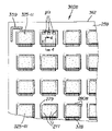
- 325 pixelated display area
- 325-11 pixelated OLED display area at a position (1;1)
- 325-13 pixelated OLED display area at a position (1;3)
- 325-14 pixelated OLED display area at a position (1;4)
- 325-21 pixelated OLED display area at a position (2;1)
- 325-31 pixelated OLED display area at a position (3;1)
- 325-xy pixelated OLED display area at a position (x;y)
- 328 outermost portion(s) of electrical interconnect area(s)
- 329 outermost portion(s) of second electrical interconnect area(s)
- 355 spacing between upper surface of encapsulation layer (310) and first surface (253) of cover plate (252)
- 357 alignment mark(s) on first surface (303) of device substrate (302)
- 359 aligned alignment marks (257 and 357)
- 360A engaged and aligned assembly configuration “A”
- 360B engaged and aligned assembly configuration “B”
- 360Bs singulated packaged OLED device (from
assembly configuration 360B) - 362 common edge(s) of aligned cover plate (252) and device substrate (302)
- 367 alternative alignment mark(s) on first surface (303) of device substrate
- 390 light emission from a pixel
- 500 power supply, scan line generator, and signal processor
- 502 signal lead
- 504 input terminal
- 510 output terminal
- 528 electrical leads
- 600 start of process
- 610 providing device substrate
- 620 providing transparent cover plate
- 630 providing flow-preventing pattern
- 640 dispensing flowable and curable adhesive material
- 650 engaging cover plate in alignment with device substrate
- 660 curing spread adhesive material
- 670 singulating device substrate and bonded cover plate
- 680 obtaining individual OLED devices having bonded cover plate
- 690 end of process
- 700 curing radiation
- EL organic electroluminescent (“EL”) medium structure
- H height dimension of flow-preventing dam pattern(s)
- pix light-emitting portion of a pixel
- sx1 spacing between OLED devices along an x-direction
- sx2 spacing between OLED devices along an x-direction, where sx2<sx1
- sx3 spacing between OLED devices along an x-direction, where sx3<sx1
- sy1 spacing between OLED devices along a y-direction
- sy2 spacing between OLED devices along a y-direction where sy2<<sy1
- x x-direction
- y y-direction
Claims (16)
Priority Applications (1)
| Application Number | Priority Date | Filing Date | Title |
|---|---|---|---|
| US10/759,914 US7279063B2 (en) | 2004-01-16 | 2004-01-16 | Method of making an OLED display device with enhanced optical and mechanical properties |
Applications Claiming Priority (1)
| Application Number | Priority Date | Filing Date | Title |
|---|---|---|---|
| US10/759,914 US7279063B2 (en) | 2004-01-16 | 2004-01-16 | Method of making an OLED display device with enhanced optical and mechanical properties |
Publications (2)
| Publication Number | Publication Date |
|---|---|
| US20050155704A1 US20050155704A1 (en) | 2005-07-21 |
| US7279063B2 true US7279063B2 (en) | 2007-10-09 |
Family
ID=34749797
Family Applications (1)
| Application Number | Title | Priority Date | Filing Date |
|---|---|---|---|
| US10/759,914 Active 2025-03-17 US7279063B2 (en) | 2004-01-16 | 2004-01-16 | Method of making an OLED display device with enhanced optical and mechanical properties |
Country Status (1)
| Country | Link |
|---|---|
| US (1) | US7279063B2 (en) |
Cited By (11)
| Publication number | Priority date | Publication date | Assignee | Title |
|---|---|---|---|---|
| US20080149380A1 (en) * | 2004-09-28 | 2008-06-26 | Rohm Co., Ltd. | Material Board for Producing Hybrid Circuit Board with Metallic Terminal Plate and Method for Producing Hybrid Circuit Board |
| US20090267891A1 (en) * | 2008-04-25 | 2009-10-29 | Bamidele Ali | Virtual paper |
| US20100107214A1 (en) * | 2008-10-27 | 2010-04-29 | Ganz | Temporary user account for a virtual world website |
| US20140346476A1 (en) * | 2013-05-24 | 2014-11-27 | Boe Technology Group Co., Ltd. | Oled display panel and the packaging method thereof, display device |
| US20140346477A1 (en) * | 2013-05-24 | 2014-11-27 | Innolux Corporation | Organic light emitting display device |
| CN104183614A (en) * | 2013-05-24 | 2014-12-03 | 群创光电股份有限公司 | Organic light emitting display device |
| WO2015180343A1 (en) * | 2014-05-29 | 2015-12-03 | 京东方科技集团股份有限公司 | Light-emitting display panel and manufacturing method therefor |
| US9978820B2 (en) * | 2015-12-31 | 2018-05-22 | Lg Display Co., Ltd. | Organic light emitting display device having a triple dam structure |
| US20190036234A1 (en) * | 2017-07-25 | 2019-01-31 | Lockheed Martin Corporation | Cable with nanoparticle paste |
| US20190234864A1 (en) * | 2013-12-12 | 2019-08-01 | G.M.S Global Mobile Solutions Ltd. | Sample holder for home testing device |
| CN110910777A (en) * | 2019-05-29 | 2020-03-24 | 友达光电股份有限公司 | Light emitting diode panel and splicing display device |
Families Citing this family (46)
| Publication number | Priority date | Publication date | Assignee | Title |
|---|---|---|---|---|
| US8288861B2 (en) * | 2004-04-22 | 2012-10-16 | Osram Opto Semiconductors Gmbh | Encapsulation for an organic electronic component, its production process and its use |
| JP2006049308A (en) * | 2004-08-04 | 2006-02-16 | Samsung Electronics Co Ltd | Display device, manufacturing method of the same, and manufacturing device for the same |
| EP1655790B1 (en) * | 2004-10-21 | 2010-08-04 | LG Display Co., Ltd. | Organic electroluminescent device and method of manufacturing the same |
| US7843134B2 (en) * | 2005-10-31 | 2010-11-30 | Idemitsu Kosan Co., Ltd. | Organic EL emission devices connected in series |
| KR100685853B1 (en) * | 2006-01-25 | 2007-02-22 | 삼성에스디아이 주식회사 | Organic electroluminescence device and method for fabricating of the same |
| KR100801623B1 (en) * | 2006-06-23 | 2008-02-11 | 삼성전자주식회사 | Manufacturing method for display device and manufacturing appratus for the same and display device made by the same |
| US20080216952A1 (en) * | 2007-03-06 | 2008-09-11 | Cheng Uei Precision Industry Co., Ltd. | Adhesive Method Of Optical Components |
| KR101096142B1 (en) * | 2008-01-24 | 2011-12-19 | 브레우어 사이언스 인코포레이션 | Method for reversibly mounting a device wafer to a carrier substrate |
| WO2009099425A2 (en) * | 2008-02-07 | 2009-08-13 | Qd Vision, Inc. | Flexible devices including semiconductor nanocrystals, arrays, and methods |
| KR100953654B1 (en) | 2008-06-26 | 2010-04-20 | 삼성모바일디스플레이주식회사 | Organic light emitting diode display and method for manufacturing the smae |
| JP5513020B2 (en) * | 2009-06-19 | 2014-06-04 | パナソニック液晶ディスプレイ株式会社 | THIN FILM TRANSISTOR SUBSTRATE AND METHOD FOR PRODUCING THIN FILM TRANSISTOR SUBSTRATE |
| KR101791580B1 (en) | 2009-10-17 | 2017-10-30 | 삼성전자주식회사 | An optical component, products including same, and methods for making same |
| KR101100955B1 (en) * | 2010-03-11 | 2011-12-29 | 삼성모바일디스플레이주식회사 | Organic light emitting display device and making method for the same |
| KR101146994B1 (en) * | 2010-06-10 | 2012-05-22 | 삼성모바일디스플레이주식회사 | A display apparatus and a method for manufacturing the same |
| US8852391B2 (en) | 2010-06-21 | 2014-10-07 | Brewer Science Inc. | Method and apparatus for removing a reversibly mounted device wafer from a carrier substrate |
| US9263314B2 (en) | 2010-08-06 | 2016-02-16 | Brewer Science Inc. | Multiple bonding layers for thin-wafer handling |
| SG179299A1 (en) * | 2010-09-13 | 2012-04-27 | Trimech Technology Pte Ltd | A display panel substrate assembly, an apparatus and a method for forming a display panel substrate assembly |
| KR102037700B1 (en) | 2012-05-23 | 2019-10-30 | 삼성디스플레이 주식회사 | Portable display device and method of assembling the same |
| US9608029B2 (en) * | 2013-06-28 | 2017-03-28 | Stmicroelectronics Pte Ltd. | Optical package with recess in transparent cover |
| KR20150025994A (en) | 2013-08-30 | 2015-03-11 | 엘지디스플레이 주식회사 | Organic light emitting diode display device and method of fabricating the same |
| EP3099215B1 (en) | 2014-01-31 | 2024-03-06 | Canon U.S.A., Inc. | Apparatus for color endoscopy |
| US10288868B2 (en) | 2014-01-31 | 2019-05-14 | Canon U.S.A., Inc. | Optical probe, light intensity detection, imaging method and system |
| EP3671883A1 (en) | 2014-06-25 | 2020-06-24 | LG Display Co., Ltd. | Organic light emitting display apparatus |
| CN104461203B (en) * | 2014-12-22 | 2017-10-27 | 合肥鑫晟光电科技有限公司 | Cover plate and the film adhered method of touch-control sensing and touch-screen |
| CN104659269B (en) * | 2015-02-06 | 2017-05-17 | 深圳市华星光电技术有限公司 | OLED encapsulation method and OLED encapsulation structure |
| US10194065B2 (en) | 2015-08-05 | 2019-01-29 | Canon U.S.A., Inc. | Endoscope probes and systems, and methods for use therewith |
| WO2017024145A1 (en) | 2015-08-05 | 2017-02-09 | Canon U.S.A., Inc. | Forward and angle view endoscope |
| US9869854B2 (en) * | 2015-12-16 | 2018-01-16 | Canon U.S.A, Inc. | Endoscopic system |
| JP2019502519A (en) | 2015-12-28 | 2019-01-31 | キヤノン ユーエスエイ, インコーポレイテッドCanon U.S.A., Inc | Optical probe, light intensity detection, imaging method and system |
| JP6670943B2 (en) | 2016-02-12 | 2020-03-25 | キヤノン ユーエスエイ, インコーポレイテッドCanon U.S.A., Inc | Simple monolithic optics for spectrally coded endoscopy of forward view |
| US10321810B2 (en) | 2016-06-13 | 2019-06-18 | Canon U.S.A., Inc. | Spectrally encoded endoscopic probe having a fixed fiber |
| KR102610024B1 (en) * | 2016-06-16 | 2023-12-06 | 삼성디스플레이 주식회사 | Display device |
| US10234694B2 (en) | 2016-07-15 | 2019-03-19 | Canon U.S.A., Inc. | Spectrally encoded probes |
| US10401610B2 (en) | 2016-07-15 | 2019-09-03 | Canon Usa, Inc. | Spectrally encoded probe with multiple diffraction orders |
| WO2018039468A1 (en) | 2016-08-26 | 2018-03-01 | Molecular Imprints, Inc. | Edge sealant confinement and halo reduction for optical devices |
| JP2019534069A (en) | 2016-09-23 | 2019-11-28 | キヤノン ユーエスエイ, インコーポレイテッドCanon U.S.A., Inc | Spectral-coded endoscopy apparatus and method |
| US10898068B2 (en) | 2016-11-01 | 2021-01-26 | Canon U.S.A., Inc. | Multi-bandwidth spectrally encoded endoscope |
| JP2018094395A (en) | 2016-11-03 | 2018-06-21 | キヤノン ユーエスエイ, インコーポレイテッドCanon U.S.A., Inc | Diagnostic spectrally encoded endoscopy apparatuses and systems, and methods for use with the same |
| KR20180094199A (en) * | 2017-02-14 | 2018-08-23 | 삼성디스플레이 주식회사 | Display device and manufacturing method of the same |
| US10825152B2 (en) | 2017-09-14 | 2020-11-03 | Canon U.S.A., Inc. | Distortion measurement and correction for spectrally encoded endoscopy |
| KR102360094B1 (en) * | 2017-09-15 | 2022-02-09 | 삼성디스플레이 주식회사 | Display device |
| US11513372B2 (en) | 2018-06-12 | 2022-11-29 | Magic Leap, Inc. | Edge sealant application for optical devices |
| JP7195419B2 (en) | 2018-10-16 | 2022-12-23 | マジック リープ, インコーポレイテッド | Method and apparatus for casting polymer products |
| CN109542269B (en) * | 2018-11-20 | 2022-05-03 | 信利(惠州)智能显示有限公司 | Touch display screen and touch display device |
| CN113471256B (en) * | 2021-06-16 | 2023-04-18 | 武汉华星光电技术有限公司 | Display panel and preparation method thereof |
| CN114078396A (en) * | 2021-11-30 | 2022-02-22 | 云谷(固安)科技有限公司 | Bonding method and bonding apparatus |
Citations (12)
| Publication number | Priority date | Publication date | Assignee | Title |
|---|---|---|---|---|
| US4657341A (en) * | 1983-08-03 | 1987-04-14 | Siemens Aktiengesellschaft | Connector for light waveguides and method of producing same |
| US6198217B1 (en) * | 1997-05-12 | 2001-03-06 | Matsushita Electric Industrial Co., Ltd. | Organic electroluminescent device having a protective covering comprising organic and inorganic layers |
| US6268695B1 (en) | 1998-12-16 | 2001-07-31 | Battelle Memorial Institute | Environmental barrier material for organic light emitting device and method of making |
| US20020074931A1 (en) * | 2000-12-20 | 2002-06-20 | Koninklijke Philips Electronics N.V. | Device, particularly an electroluminescent display device, and method of manufacturing such a device |
| US20020155320A1 (en) | 2001-04-20 | 2002-10-24 | Lg.Philips Lcd Co., Ltd. | Organic electroluminescent device |
| US20020187775A1 (en) | 1999-12-13 | 2002-12-12 | Louis Corrigan | WAP service personalisation, management and billing object oriented platform |
| US20020193035A1 (en) | 2001-06-14 | 2002-12-19 | Mao-Kuo Wei | Package method and apparatus for organic electro-luminescent display |
| US20030067268A1 (en) * | 2001-09-28 | 2003-04-10 | Hideki Matsuoka | Method of manufacturing electroluminescence panel |
| US20030218442A1 (en) * | 2002-05-25 | 2003-11-27 | Motorola, Inc. | Methods and devices for controlling stepper motors |
| US20030218422A1 (en) * | 2002-05-23 | 2003-11-27 | Samsung Sdi Co., Ltd. | Method for encapsulating organic electroluminescent device and an organic electroluminescent panel using the same |
| US20050002081A1 (en) * | 2001-09-14 | 2005-01-06 | Fabien Beteille | Functional safety glazing unit |
| US6867539B1 (en) * | 2000-07-12 | 2005-03-15 | 3M Innovative Properties Company | Encapsulated organic electronic devices and method for making same |
-
2004
- 2004-01-16 US US10/759,914 patent/US7279063B2/en active Active
Patent Citations (12)
| Publication number | Priority date | Publication date | Assignee | Title |
|---|---|---|---|---|
| US4657341A (en) * | 1983-08-03 | 1987-04-14 | Siemens Aktiengesellschaft | Connector for light waveguides and method of producing same |
| US6198217B1 (en) * | 1997-05-12 | 2001-03-06 | Matsushita Electric Industrial Co., Ltd. | Organic electroluminescent device having a protective covering comprising organic and inorganic layers |
| US6268695B1 (en) | 1998-12-16 | 2001-07-31 | Battelle Memorial Institute | Environmental barrier material for organic light emitting device and method of making |
| US20020187775A1 (en) | 1999-12-13 | 2002-12-12 | Louis Corrigan | WAP service personalisation, management and billing object oriented platform |
| US6867539B1 (en) * | 2000-07-12 | 2005-03-15 | 3M Innovative Properties Company | Encapsulated organic electronic devices and method for making same |
| US20020074931A1 (en) * | 2000-12-20 | 2002-06-20 | Koninklijke Philips Electronics N.V. | Device, particularly an electroluminescent display device, and method of manufacturing such a device |
| US20020155320A1 (en) | 2001-04-20 | 2002-10-24 | Lg.Philips Lcd Co., Ltd. | Organic electroluminescent device |
| US20020193035A1 (en) | 2001-06-14 | 2002-12-19 | Mao-Kuo Wei | Package method and apparatus for organic electro-luminescent display |
| US20050002081A1 (en) * | 2001-09-14 | 2005-01-06 | Fabien Beteille | Functional safety glazing unit |
| US20030067268A1 (en) * | 2001-09-28 | 2003-04-10 | Hideki Matsuoka | Method of manufacturing electroluminescence panel |
| US20030218422A1 (en) * | 2002-05-23 | 2003-11-27 | Samsung Sdi Co., Ltd. | Method for encapsulating organic electroluminescent device and an organic electroluminescent panel using the same |
| US20030218442A1 (en) * | 2002-05-25 | 2003-11-27 | Motorola, Inc. | Methods and devices for controlling stepper motors |
Cited By (26)
| Publication number | Priority date | Publication date | Assignee | Title |
|---|---|---|---|---|
| US20080149380A1 (en) * | 2004-09-28 | 2008-06-26 | Rohm Co., Ltd. | Material Board for Producing Hybrid Circuit Board with Metallic Terminal Plate and Method for Producing Hybrid Circuit Board |
| US7943860B2 (en) * | 2004-09-28 | 2011-05-17 | Rohm Co., Ltd. | Material board for producing hybrid circuit board with metallic terminal plate and method for producing hybrid circuit board |
| US20090267891A1 (en) * | 2008-04-25 | 2009-10-29 | Bamidele Ali | Virtual paper |
| US20100107214A1 (en) * | 2008-10-27 | 2010-04-29 | Ganz | Temporary user account for a virtual world website |
| US8516553B2 (en) | 2008-10-27 | 2013-08-20 | Ganz | Temporary user account for a virtual world website |
| US8826383B2 (en) | 2008-10-27 | 2014-09-02 | Ganz | Temporary user account for a virtual world website |
| CN104183614B (en) * | 2013-05-24 | 2017-06-06 | 群创光电股份有限公司 | Organic light-emitting display device |
| CN104183614A (en) * | 2013-05-24 | 2014-12-03 | 群创光电股份有限公司 | Organic light emitting display device |
| US8969904B2 (en) * | 2013-05-24 | 2015-03-03 | Innolux Corporation | Organic light emitting display device |
| US20140346477A1 (en) * | 2013-05-24 | 2014-11-27 | Innolux Corporation | Organic light emitting display device |
| US20140346476A1 (en) * | 2013-05-24 | 2014-11-27 | Boe Technology Group Co., Ltd. | Oled display panel and the packaging method thereof, display device |
| US20190234864A1 (en) * | 2013-12-12 | 2019-08-01 | G.M.S Global Mobile Solutions Ltd. | Sample holder for home testing device |
| US10935484B2 (en) | 2013-12-12 | 2021-03-02 | Mes Medical Electronic Systems Ltd. | Automated assessment of sperm samples |
| US10859488B2 (en) * | 2013-12-12 | 2020-12-08 | Mes Medical Electronic Systems Ltd. | Sample holder for home testing device |
| US9502678B2 (en) | 2014-05-29 | 2016-11-22 | Boe Technology Group Co., Ltd. | Light emitting display panel and manufacturing method thereof |
| US9985244B2 (en) | 2014-05-29 | 2018-05-29 | Boe Technology Group Co., Ltd. | Light emitting display panel and manufacturing method thereof |
| WO2015180343A1 (en) * | 2014-05-29 | 2015-12-03 | 京东方科技集团股份有限公司 | Light-emitting display panel and manufacturing method therefor |
| US10304916B2 (en) | 2015-12-31 | 2019-05-28 | Lg Display Co., Ltd. | Organic light emitting display device having a non-display area dam structure |
| US9978820B2 (en) * | 2015-12-31 | 2018-05-22 | Lg Display Co., Ltd. | Organic light emitting display device having a triple dam structure |
| US10916604B2 (en) | 2015-12-31 | 2021-02-09 | Lg Display Co., Ltd. | Organic light emitting display device having a multi-directional dam structure |
| US11552141B2 (en) | 2015-12-31 | 2023-01-10 | Lg Display Co, Ltd. | Organic light emitting display device including curve-shaped third dam structure |
| US11968860B2 (en) | 2015-12-31 | 2024-04-23 | Lg Display Co., Ltd. | Organic light emitting display device including dam structure and alignment mark |
| US20190036234A1 (en) * | 2017-07-25 | 2019-01-31 | Lockheed Martin Corporation | Cable with nanoparticle paste |
| US11031704B2 (en) * | 2017-07-25 | 2021-06-08 | Lockheed Martin Corporation | Cable with nanoparticle paste |
| CN110910777A (en) * | 2019-05-29 | 2020-03-24 | 友达光电股份有限公司 | Light emitting diode panel and splicing display device |
| US11195970B2 (en) * | 2019-05-29 | 2021-12-07 | Au Optronics Corporation | Light emitting diode panel and tiling display apparatus |
Also Published As
| Publication number | Publication date |
|---|---|
| US20050155704A1 (en) | 2005-07-21 |
Similar Documents
| Publication | Publication Date | Title |
|---|---|---|
| US7279063B2 (en) | Method of making an OLED display device with enhanced optical and mechanical properties | |
| CN108123062B (en) | Organic light emitting display device | |
| CN106876328B (en) | OLED display panel, preparation method thereof and display device | |
| US7932670B2 (en) | Organic electro-luminescence display device and method of manufacturing the same | |
| KR100707544B1 (en) | Organic electroluminescence display device | |
| US7144752B2 (en) | Method of manufacturing organic electroluminescent display device and organic electroluminescent display device, and display device equipped with organic electroluminescent display device | |
| KR101301180B1 (en) | Dual Plate Type Organic Electro-luminescent Device and the method for | |
| JP7443650B2 (en) | Display substrate, display device, and display substrate manufacturing method | |
| WO2019041945A1 (en) | Display substrate and manufacturing method therefor, and display panel | |
| US10276812B2 (en) | Display device and manufacturing method thereof | |
| JP2008235089A (en) | Organic el display panel and its manufacturing method | |
| CN108417598B (en) | OLED display panel, packaging method and preparation method of organic film | |
| US7135352B2 (en) | Method of fabricating a cover plate bonded over an encapsulated OLEDs | |
| WO2019109692A1 (en) | Electronic apparatus substrate and manufacturing method, and display apparatus | |
| KR102583813B1 (en) | Display apparatus | |
| KR100703457B1 (en) | Organic light emitting display device and fabricating method of the same | |
| TW201415624A (en) | Organic light emitting diode display and method for manufacturing the same | |
| KR100963073B1 (en) | Organic light emitting display device | |
| KR20150006706A (en) | Organic light emitting display device and method of fabricating thereof | |
| KR20070078502A (en) | Organic light emitting display and fabrication method for the same | |
| KR102094143B1 (en) | Fabricating Method Of Organic Light Emitting Diode Display | |
| CN108666437B (en) | Display panel and manufacturing method thereof | |
| CN112289948B (en) | Organic light emitting diode display panel and manufacturing method thereof | |
| KR20140074774A (en) | Organic light emitting display device and method of fabricating thereof | |
| KR100815761B1 (en) | Manufacturing method of organic light emitting display device |
Legal Events
| Date | Code | Title | Description |
|---|---|---|---|
| AS | Assignment |
Owner name: EASTMAN KODAK COMPANY, NEW YORK Free format text: ASSIGNMENT OF ASSIGNORS INTEREST;ASSIGNORS:YOKAJTY, JOSEPH E.;SERBICKI, JEFFREY P.;VANSLYKE, STEVEN A.;REEL/FRAME:014904/0569;SIGNING DATES FROM 20031215 TO 20031222 |
|
| FEPP | Fee payment procedure |
Free format text: PAYOR NUMBER ASSIGNED (ORIGINAL EVENT CODE: ASPN); ENTITY STATUS OF PATENT OWNER: LARGE ENTITY |
|
| STCF | Information on status: patent grant |
Free format text: PATENTED CASE |
|
| FEPP | Fee payment procedure |
Free format text: PAYER NUMBER DE-ASSIGNED (ORIGINAL EVENT CODE: RMPN); ENTITY STATUS OF PATENT OWNER: LARGE ENTITY Free format text: PAYOR NUMBER ASSIGNED (ORIGINAL EVENT CODE: ASPN); ENTITY STATUS OF PATENT OWNER: LARGE ENTITY |
|
| AS | Assignment |
Owner name: GLOBAL OLED TECHNOLOGY LLC,DELAWARE Free format text: ASSIGNMENT OF ASSIGNORS INTEREST;ASSIGNOR:EASTMAN KODAK COMPANY;REEL/FRAME:023998/0368 Effective date: 20100122 Owner name: GLOBAL OLED TECHNOLOGY LLC, DELAWARE Free format text: ASSIGNMENT OF ASSIGNORS INTEREST;ASSIGNOR:EASTMAN KODAK COMPANY;REEL/FRAME:023998/0368 Effective date: 20100122 |
|
| FPAY | Fee payment |
Year of fee payment: 4 |
|
| FPAY | Fee payment |
Year of fee payment: 8 |
|
| MAFP | Maintenance fee payment |
Free format text: PAYMENT OF MAINTENANCE FEE, 12TH YEAR, LARGE ENTITY (ORIGINAL EVENT CODE: M1553); ENTITY STATUS OF PATENT OWNER: LARGE ENTITY Year of fee payment: 12 |