US7284227B1 - Method and system for generating implementation files from a high level specification - Google Patents
Method and system for generating implementation files from a high level specification Download PDFInfo
- Publication number
- US7284227B1 US7284227B1 US10/966,993 US96699304A US7284227B1 US 7284227 B1 US7284227 B1 US 7284227B1 US 96699304 A US96699304 A US 96699304A US 7284227 B1 US7284227 B1 US 7284227B1
- Authority
- US
- United States
- Prior art keywords
- block
- blocks
- file
- bump
- lay
- Prior art date
- Legal status (The legal status is an assumption and is not a legal conclusion. Google has not performed a legal analysis and makes no representation as to the accuracy of the status listed.)
- Expired - Fee Related, expires
Links
Images


Classifications
-
- G—PHYSICS
- G06—COMPUTING; CALCULATING OR COUNTING
- G06F—ELECTRIC DIGITAL DATA PROCESSING
- G06F30/00—Computer-aided design [CAD]
- G06F30/30—Circuit design
- G06F30/34—Circuit design for reconfigurable circuits, e.g. field programmable gate arrays [FPGA] or programmable logic devices [PLD]
Definitions
- This application includes a computer program-listing appendix on a single compact disc, the contents of which are incorporated herein by reference in their entirety.
- the compact disc contains a first 10 KB file entitled “4vfx20.txt” created Jun. 9, 2004, a second 236 KB file entitled “dgen.c_excerpts.txt” created Sep. 20, 2004, a third 7 KB file entitled “4vfx12.txt” created Jul. 1, 2004, a fourth 3 KB file entitled “4vfx20.combos.txt” created Jun. 9, 2004, a fifth 26 KB file entitled “4vfx20.con.txt” created Jun.
- the present invention relates generally to computer aided design of integrated circuits (ICs).
- CAD Computer Aided design
- CAD tools have been used to produce programmable logic devices (PLDs) such as field programmable gate arrays (FPGAs).
- PLDs programmable logic devices
- FPGAs field programmable gate arrays
- FIG. 1 is a simplified schematic view of a conventional FPGA 48 .
- the FPGA includes a programmable fabric 2 surrounded by an I/O ring 4 .
- the programmable fabric 2 includes configurable logic block (CLB) columns 5 , block random access memory (BRAM) columns 6 , and a digital signal processing (DSP) column 7 .
- the I/O ring 4 includes input/output blocks (IOBs) and multi-gigabit transceiver (MGT) blocks (not shown).
- a programmable interconnect structure (not shown in FIG. 1 ) allows the circuit elements or blocks in the programmable fabric to be interconnected with each other and with the circuit elements or blocks in the I/O ring 4 .
- the present invention relates generally to a method and system for generating from a high-level placement specification the layout and schematic implementation data.
- packaging data and/or software modeling data may also be generated.
- an array of rows and columns is formed on an integrated circuit (IC) in which most elements in a row have substantially the same height and most elements in a column have substantially the same width.
- This array which may be formed in a textual or spreadsheet format, forms the high-level placement specification.
- a software program of this embodiment converts this high-level placement specification into layout and schematic files that can be used by a commercial CAD tool to produce a file for fabrication.
- the software program may also receive package pin list information, which the program uses to generate device packaging data.
- One embodiment of the present invention includes a system using a computer for laying out blocks from a common specification.
- the system includes: a high level block placement specification, e.g., a spreadsheet, stored in a computer readable medium, having a description of blocks arranged in rows and columns, wherein substantially all blocks in a row are of substantially equal height and substantially all blocks in a column are of substantially equal width; a bump placement specification for selected blocks; and software configured to lay out the plurality of blocks and to place one or more bumps on each selected block using the high level block placement specification and the bump placement specification.
- a high level block placement specification e.g., a spreadsheet
- a computer readable medium having a description of blocks arranged in rows and columns, wherein substantially all blocks in a row are of substantially equal height and substantially all blocks in a column are of substantially equal width
- a bump placement specification for selected blocks
- software configured to lay out the plurality of blocks and to place one or more bumps on each selected block using the high level block placement specification and the bump
- Another embodiment of the present invention includes a method for creating a package file for an integrated circuit. First, a grid is formed having a plurality of blocks. Next, a height and a width is determined for each block. Then at least one bump is placed on a block and a corresponding package pin is assigned to the at least one bump. Lastly, the package file is outputted.
- Yet another embodiment of the present invention includes software code stored in a computer readable medium for creating implementation files for a programmable logic device (PLD).
- the software code includes: code for receiving an array of rows and columns, where the array has a plurality of blocks, wherein each block is placed in an intersection of a row and a column; code for receiving data for setting a height for each row and a width for each column; code for determining a height, a width and a coordinate for each block; code for placing at least one bump on a block; code for assigning to the at least one bump a corresponding package pin; and code for outputting a package file, a layout file, a software model file, and a schematic file.
- a further embodiment of the present invention includes a system using a computer for creating implementation files for a programmable logic design.
- the system includes: a spreadsheet, displayed on a computer display, having an assignment of a plurality of blocks to spreadsheet cells, wherein substantially all blocks in a row of the spreadsheet are of substantially equal height and substantially all blocks in a column of the spreadsheet are of substantially equal width; a blocks definition file defining layout height and width for a block; and a software program configured to generate a layout implementation file based on input from the spreadsheet and blocks definition file.
- FIG. 1 is a simplified schematic view of a conventional FPGA (PRIOR ART);
- FIG. 2 is a simplified diagram of an IC in accordance with one embodiment of the present invention.
- FIG. 3 illustrates FPGA architecture of another embodiment of the present invention that includes a large number of different programmable tiles
- FIGS. 4A and 4B are simplified diagrams of a FPGA in accordance with another embodiment of the present invention.
- FIGS. 5A-5C is a spreadsheet showing the high-level block placement for part of a FPGA of an embodiment of the present invention.
- FIG. 6 is block diagram of a system of an embodiment of the present invention.
- FIGS. 7A and 7B show two examples of common data structures of an embodiment of the present invention.
- FIG. 8 is a flowchart for creating a package file and Cadence SKILL files for an integrated circuit of an embodiment of the present invention.
- Cadence® SKILL language is a high-level programming language, based on the LISP programming language but uses a C-like syntax. It is accessible only from within the Cadence software.
- FIG. 9 is a block diagram of a system using a master database to produce multiple views of a columnar architecture design of an embodiment of the present invention.
- the integrated circuit is divided into an array of multiple rows and multiple columns.
- the intersection of a row and a column includes a block, where the block has one or more circuit components or elements.
- most blocks (to substantially all blocks) in a column have the same physical width and most blocks (to substantially all blocks) in a row have the same physical height.
- Two columns do not necessarily have the same width and two rows do not necessarily have the same height.
- a mega-block i.e., a set of adjacent blocks, may be used to accommodate a multi-block application specific circuit, for example, a microprocessor.
- a high level block placement specification placing the blocks is formed by the user.
- This high level block placement specification can have many forms.
- a spreadsheet such as shown in FIGS. 5A-5C can be used to place some of the blocks.
- a textual description having a line of codes for each row (or column), for example, “t.4.i.4.b.4.d.4.o.4.b.4.i.4.t”, can alternatively be used to place the blocks per row (or column).
- the textual description having a line of codes can first be used and a PERL script used to expand the codes to produce the spreadsheet.
- One major advantage of using, for example, a spreadsheet is that columns (and/or rows) can be easily moved, added or subtracted, or modified.
- a columnar architecture e.g., FIGS. 2 , 3 , and 4 A/B
- laying out a new IC with a different mix of column types can be done in substantially less time than can be conventionally done.
- a design generator software program uses this high level placement specification along with detailed block and bump placement information for each block type to produce layout and schematic implementation data, for example, SKILL files.
- This implementation data is used, in a well-known process, by a commercial CAD tool, for example the Virtuoso custom design platform from Cadence Inc., along with a cell library provided by the user, to produce the GDSII Stream data (which may be used for electron beam lithography and photo mask production of the IC).
- pin list for a particular package can be input into the design generator software program and the bumps mapped to the pins.
- a package file can be produced such that the manufactures IC can be easily packaged.
- a software model may also be produced for simulation and verification.
- the files needed to manufacture, package and simulate the IC design are generated by one software program (which may or may not be distributed in one or more sections of code).
- the software program uses common data structures which allow for the sharing of information in generating the different output files.
- the common data structures are stored in a computer readable medium.
- the common data structures are stored in a database (DB), which may include a flat file. This is an improvement over prior art where the same data had to be entered in different locations, hence increasing the possibility of error and implementation time, especially if there was a change in the data.
- the regular structure of the array and of the block types allows for parameterization of data describing the blocks in an embodiment of the present invention.
- the block (or cell) placement including offset values can be done using algebraic equations and/or variables.
- a block width in a column can, for example, be given by a variable which is set in a common location.
- a block location in a row/column intersection in the array can be given, for example, by an algebraic equation using the center point of the row/column intersection and an (x,y) offset, where the offset is set in a common location.
- This algebraic representation of block or cell placement allows for easy updates.
- a more general functional representation i.e., f(x,y), may be used.
- one or more templates are used to place the bumps associated with, for example, the IOBs or MGTs in a PLD.
- each IOL 215 can be separately specified in an IOB specification that is read and implemented by the software program.
- each IOB block or pair of blocks can be given an IOB type name.
- the description of the 16 IOLs can be looked up in, for example, an IOB options file. Modifications to the IOLs associated with an IOB type name can be done in one location with the software program automatically placing the 16 IOLs and associated bumps.
- FIGS. 2 , 3 , and 4 A/B An illustrative example of a columnar architecture is used ( FIGS. 2 , 3 , and 4 A/B).
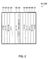
- FIG. 2 is a simplified diagram of IC 100 in accordance with one embodiment of the present invention.
- the IC includes two or more homogeneous columns, wherein each of the homogeneous columns starts at one side of the IC and ends at an opposite side of the IC.
- Each homogeneous column has substantially identical circuit elements substantially filling the column.
- IC 100 includes homogeneous columns 52 , 58 , and 64 of a CLB column type, homogeneous columns 54 and 68 of a BRAM column type, homogeneous columns 56 and 66 of an IOB column type, homogeneous column 62 of a DSP column type, and homogeneous column 70 of a MGT column type.
- FIG. 2 there is a heterogeneous column 60 (center col.) that may have circuit elements of different circuit types.
- FIG. 2 does not have an I/O ring 2 .
- Note some embodiments of the present invention can be used for producing the FPGA 48 in FIG. 1 as well as for producing the IC 100 in FIG. 2 .
- FIG. 3 illustrates a FPGA architecture 200 of another embodiment of the present invention.
- FPGAs are a specific type of PLDs.
- Another example of a PLD includes a complex programmable logic device (CPLD).
- FPGA 200 has a large number of different programmable tiles including multi-gigabit transceivers (MGTs 201 ), configurable logic blocks (CLBs 202 ), random access memory blocks (BRAMs 203 ), input/output blocks (IOBs 204 ), configuration and clocking logic (CONFIG/CLOCKS 205 ), digital signal processing blocks (DSPs 206 ), specialized input/output blocks (I/O 207 ) (e.g., configuration ports and clock ports), and other programmable logic 208 such as digital clock managers, analog-to-digital converters, system monitoring logic, and so forth.
- This FPGA may also include dedicated processor blocks (PROC 210 ).
- Each programmable tile includes a programmable interconnect element (INT 211 ) having standardized connections to and from a corresponding interconnect element in each adjacent tile. Therefore, the programmable interconnect elements taken together implement the programmable interconnect structure for the illustrated FPGA 200 .
- the programmable interconnect element (INT 211 ) also includes the connections to and from the programmable logic element within the same tile, as shown by the examples included at the top of FIG. 3 .
- a CLB 202 can include a configurable logic element (CLE 212 ) that can be programmed to implement user logic plus a single programmable interconnect element (INT 211 ).
- a BRAM 203 can include a BRAM logic element (BRL 213 ) in addition to one or more programmable interconnect elements.
- BRAM logic element BRAM logic element
- the number of interconnect elements included in a tile depends on the height of the tile. In the pictured embodiment, a BRAM tile has the same height as four CLBs, but other numbers (e.g., five) can also be used.
- a DSP tile 206 can include a DSP logic element (DSPL 214 ) in addition to an appropriate number of programmable interconnect elements.
- An IOB 204 can include, for example, two instances of an input/output logic element (IOL 215 ) in addition to one instance of the programmable interconnect element (INT 211 ).
- IOL 215 input/output logic element
- INT 211 programmable interconnect element
- the actual I/O pads connected, for example, to the I/O logic element 215 are manufactured using metal layered above the various illustrated logic blocks, and typically are not confined to the area of the input/output logic element 215 .
- a columnar area near the center of the die (shown shaded in FIG. 3 ) is used for configuration, clock, and other control logic. Horizontal areas 209 extending from this column are used to distribute the clocks and configuration signals across the breadth of the FPGA.
- the architecture illustrated in FIG. 3 includes additional logic blocks that disrupt the regular columnar structure making up a large part of the FPGA.
- the additional logic blocks can be programmable blocks and/or dedicated logic.
- the processor block PROC 210 shown in FIG. 3 spans several columns of CLBs and BRAMs.
- FIG. 3 is intended to illustrate only an exemplary embodiment.
- the numbers of logic blocks in a column, the relative widths of the columns, the number and order of columns, the types of logic blocks included in the columns, the relative sizes of the logic blocks, and the interconnect/logic implementations included at the top of FIG. 3 are purely exemplary.
- FIGS. 4A and 4B are simplified diagrams of a FPGA in accordance with another embodiment of the present invention.
- FIG. 4A shows a block diagram of the left side of the FPGA with the right side being shown in FIG. 4B . Note that the diagrams in FIGS. 4A and 4B are not to scale and that row 348 has been expanded to show the details.
- FIGS. 4A and 4B the horizontal hclk rows of a H clock tree are labeled by 340 . Note that the term's row and column are for explanation purposes only and can be interchanged.
- the hclk rows are coupled to the backbone or main trunk 42 (gclk) of the H clock tree.
- Rows 342 A ( FIG. 4A) and 342B ( FIG. 4B ) each have 12 IOB groups, where each IOB group has 8 IOBs (or 16 IOLs, see FIG. 3 ).
- Rows 343 A- 343 N each have 12 CLB groups, where from FIG. 3 each CLB group has 8 CLBs.
- Rows 344 A- 344 C each have 12 BRAMs, where from FIG. 3 each BRAM has 2 BRLs.
- Row 345 has 24 DSP blocks.
- Row 346 in FIG. 4A is the center column 60 of FIG. 2 and includes a plurality of heterogeneous elements, such as (from bottom to top) a System Monitor (Sys Mon) block, 3 DCM blocks, a CCM block, 2 IOBs, a CFG_center 20 , 2 IOBS, a CCM block, and 5 DCM blocks.
- Row 348 is adjacent to row 346 and has the circuit blocks which interface the hclk rows 340 and the blocks in row 346 to the global clock tree backbone 42 (gclk).
- FIGS. 5A-5C is a spreadsheet showing the high-level block placement for part of a FPGA of an embodiment of the present invention.
- FIGS. 5A-5C is the high-level placement specification for part of the associated FPGA 300 of FIGS. 4A-4B .
- Related columns in FIGS. 5A-5C have been given the same column reference numbers as in FIGS. 4A-4B .
- a block label iob_iob16ta(1,2) includes 1 column and 2 rows, and represents two blocks 352 - 1 and 352 - 2 , where each block has 4 IOBs (or 8 IOLs see FIG. 3 ).
- a block label clb8x2nb(1,2) includes 1 column and 2 rows, and represents two blocks 350 - 1 and 350 - 2 , where each block has 4 CLBs 202 (see FIG. 3 ).
- a block label cfg_hclk_clbx2nb_left 353 is for one block in an hclk row of the H clock tree.
- the high-level placement specification as illustrated by FIGS. 5A-C is then converted into a text file using, for example, the spreadsheet export option.
- the text file is converted into an input text format (device.con), an example of which is the file 4vfx20.con in the Appendix.
- FIG. 6 is block diagram of a system of an embodiment of the present invention.
- the software program that converts the high-level placement specification to the SKILL files used by the Virtuoso custom design platform from Cadence Inc. is called the design generator program 616 .
- the design generator program 616 is stored in a computer readable medium and is executed by a computer processor.
- the design generator program 616 receives an input run file 612 , e.g., device.in, which includes device.con (the high-level placement specification), and a package pin list file 614 , e.g., package.txt.
- the design generator program 616 works in conjunction with common data structures 615 stored in a computer readable medium.
- the design generator program 616 outputs a package file 620 , e.g., devicepackage.pkg, a software model file 622 , e.g., device.sw, a probe file 623 having a listing of the probe coordinates used by test engineering, and a layout and a schematic SKILL file 624 , e.g., layout.il and schematic.il.
- the SKILL files 624 are combined with a known cell library 628 , e.g., a FPGA cell library, by a commercial layout program 626 to produce a STREAM file 630 for IC fabrication, as is well-known in the art.
- a known cell library 628 e.g., a FPGA cell library
- a commercial layout program 626 to produce a STREAM file 630 for IC fabrication, as is well-known in the art.
- Table 1 below describes in further detail the input files to the design generator program 616 . Examples of these files for the 4vfx20 device along with an example of the design generator program 616 (dgen.c_excerpts.txt) are given in the Appendix, which is herein incorporated by reference.
- SkillLayFileName “4vfx20_lay.il” # Name of layout skill file generated.
- SkillSchFileName “4vfx20_sch.il” # Name of schematic skill file generated.
- SchLibName “wht_top” # Default schematic library name (used for all top schems).
- LayLibName “wht_top” # Default layout library name (used for all top layouts).
- FIGS. 7A and 7B show two examples of common data structures 615 of an embodiment of the present invention. Other examples are shown in the “dgen.c_excerpts.txt” file in the Appendix.
- FIG. 7A is a C language type definition structure for a block (or cell). The data structure has an entry for the block name on the spreadsheet such as shown in FIGS. 5A-5C . There are also entries for both layout and schematic block placement data for the block.
- FIG. 7B is a C language type definition structure identifying the output data produced by the design generator program.
- the chip is divided up into rows and columns. At the intersection of a row and column a block or cell exists. All blocks in a column are initially allocated the same width (but not necessarily the same height). All blocks in a row are initially allocated the same height (but not necessarily the same width). This facilitates the exchange of one column with another column (or one row with another row). Mega-blocks (or mega-cells) which are wider and/or higher then one column or one row are allowed as long as they take up integer multiples of the corresponding blocks.
- a block may consist of multiple circuit elements of the same type.
- clb8x2nb(1,2) in column 343 A of FIG. 5A consists of two blocks 350 - 1 and 350 - 2 .
- Each block has four substantially identical CLBs 202 (see FIG. 3 ).
- Block 350 - 1 has the same width as block 350 - 2 as they are in the same column.
- Block 350 - 1 (CLB) has the same height as block 352 - 1 (IOB) as they are in the same row.
- These initial layout allocations of all blocks in a column having the same width and all blocks in a row having the same height may be modified as a block in a particular row and column may be bigger than the initial layout allocation and may overlap with one or more adjacent rows/columns.
- a block in an adjacent row and column may need to be offset to accommodate the oversized block.
- the clk_hrow block 354 in FIG. 5C in column 348 is “2 clb's+hclk” tall, even though the height of the associated row is “hclk”.
- the blocks placed above (e.g., block clk_dcm_top_u) and below (e.g., block clk_dcm_top_d) block 354 are then placed with an offset to account for the block 354 overlapping into their position.
- one embodiment of the present invention includes a system using a computer for laying out blocks from a specification.
- the system includes: a high level block placement specification stored in a computer readable medium having a description of a plurality of blocks arranged in rows and columns, wherein substantially all blocks in a row are initially allocated space of substantially equal height and substantially all blocks in a column are initially allocated space of substantially equal width; an offset specification (for example, inc_block_offsets.txt in the Appendix) stored in a computer readable medium having offsets for predetermined blocks of the plurality of blocks; and software (e.g., dgen.c) configured to lay out the plurality of blocks and to place one or more bumps on each selected block using the high level block placement specification and the offset specification.
- a particular predetermined block has an adjacent block whose height or width exceeds the initially allocated space for height or width for that adjacent block.
- a block may consist of multiple circuits of the same type, e.g., IOB, but different sub-types.
- IOB iob_iob16ta(1,2)
- iob_iob16ta(1,2) occupies two blocks 352 - 1 and 352 - 2 .
- the 16 IOL 215 (see FIG. 3 ) circuits in the two blocks 352 - 1 and 352 - 2 can be individually specified in an inc_iob.options file, an example of which is given in the Appendix.
- MY indicates that the layout is flipped about the Y axis (the 1st coordinate is the layout, and the 2 nd coordinate is the schematic), R0 indicates that there is no rotation for the schematic cell placement, “lp” is one IOB subtype circuit (“iob_opt”) and “ssp” another subtype circuit (“iob_opt_lc”).
- iob _cells ⁇ “ iob — iob 16 ta ”, MY(758.62, 818.4), R0(58.1875, 67.5), lp, ln, lp, ln, lp, ln, lp, lnvr, lp, ln, lp, ln, lp, ln, ssp, ssn ⁇ , . . .
- Each block can have 4 addressable circuit elements.
- the base 4 address decoder circuitry i.e., four address decoder circuits (one for each of the four addresses), e.g., addr_cells, can be automatically inserted in the hclk block, e.g., cfg_hclk_clbx2nb_left 353 , for CLB block 350 - 1 (see FIG. 4A ).
- the placement of the two sets address decoder circuitry (where each set has four address decoder circuits) for blocks 350 - 1 and 350 - 2 is given in the file inc_addr.file, an example of which is given in the Appendix.
- the address syntax is ⁇ “block_name”, [(lay_address_offset1), (sch_address_offset1)], . . . ⁇
- the address_offset1 specifies the x,y location of the 1st address placement relative to that block [(x,y) layout offset pair followed by (x,y) schematic offset pair).
- the address_offset2 specifies the start of the 2nd address placement and so forth.
- An example code snippet is: ⁇ “cfg_hclk_clbx2nb_left”, (0, 0), (7.625, hclk_sy-1), (c1b —lx, 0), (16.625, hclk_sy-1) ⁇ where hclk_sy and clb_lx are variables given in the file inc_blocks.define (see Appendix for example).
- the example shows that two sets of address decoder circuitry will be placed. For the schematic, the first set has (x,y) offsets (0,0) and the second set has (x,y) offsets (clb_lx, 0). Similarly, (7.625, hclk_sy ⁇ 1) and (16.625, hclk_sy ⁇ 1) give the (x,y) offsets for the layout.
- each address decoder instance handles four address bits and has four address decoder circuits. These 2 instances are written left to right.
- An example of code illustrating the writing for a schematic of one address decoder instance is:
- FIG. 8 is a flowchart for creating a package file and Cadence SKILL files for an integrated circuit of an embodiment of the present invention.
- a grid of rows and columns for example a spreadsheet, is formed and the width of each column and the height of each row are determined.
- a first column may (or may not) have a different width than a second column and a first row may (or may not) have a different height than a second row.
- the width and height for each block is determined.
- the coordinates for each block of the grid is determined.
- selecting, for example, an input/output block one or more bumps are placed on the input/output block (step 714 ).
- Corresponding package pins are assigned to the one or more bumps (step 716 ).
- the package file and layout and schematic SKILL files are output (steps 718 and 720 , respectively).
- the “main” routine of the dgen.c program reads the input run file 612 and the package pinlist file 614 and produces the package file 620 , software file 622 and SKILL files 624 of FIG. 6 .
- An example main procedure is:
- MakeData in one embodiment performs steps 710 to 716 of FIG. 8 .
- the design generator program 616 determines the width of each column for all columns, height of each row for all rows, and the height and width of all blocks.
- An output produced may be of the form:
- w/h_col/row_num width and height of an intersection of a particular column and row number, col:row_num
- w/h_col/row_num width and height of an intersection of a particular column and row number, col:row_num
- inst ⁇ >banknum_exists construct ⁇ >banknum_exists
- inst ⁇ >banknum construct ⁇ >banknum
- inst ⁇ >order_exists construct ⁇ order_exists
- inst ⁇ >order construct ⁇ >order
- if (cell) part ⁇ >insts_lrtb inst
- cell NULL
- if (part>cols ⁇ inst ⁇ >col) part ⁇ >cols inst ⁇ >col
- if (part ⁇ >rows ⁇ inst ⁇ >row) part ⁇ >rows inst ⁇ >row
- InsertInst( part, inst ); ⁇ ⁇ ⁇ else ⁇ . . . ); ⁇ construct construct ⁇ >next; ⁇ . . .
- step 714 is done before step 712 in FIG. 8 .
- Step 714 places one or more bumps on each of selected blocks (normally not all blocks have bumps). All blocks with the same name get the same bumps. Which bumps go with which blocks is set by the inc_bumps.file, a sample of which is given in the Appendix, along with the name of the block. Bump positions (x,y) on a block are determined by adding the respective bump offset with the coordinates of the block placement (the calculation of the bumps x,y coordinates can be done by the CalcPart routine, a sample of which is given in the Appendix). An output of this step can be of the form:
- a template system is used by an embodiment of the present invention.
- inc_bumps.file which block names on the spreadsheet, e.g., iob_iob16ta 352 - 1 and 352 - 2 of FIG. 4A , and the associate template is first given.
- the bump allocation template syntax is:
- the bump allocation template which assigns the bumps to the block has syntax:
- the code snippet illustrating step 714 of placing bumps on each block is:
- step 712 the block placement coordinates are determined.
- the center of each row, column intersection is determined and an inputted x,y offset is used to determine the block placement.
- This step produces output of the form:
- Step 715 There may be a step 715 between steps 714 and 716 (not shown in FIG. 8 ).
- Step 715 would include assigning bump numbers.
- This step assigns unique numbers to each bank of multi-gigabit (MGT) blocks and serial I/O (SIO) blocks. The unique numbers are assigned numerically starting in the top left and increasing top to bottom/left to right. It also assigns unique PAD numbers for each I/O in the SIO blocks, again starting in the top left and increasing top to bottom/left to right.
- Example code to assign Pad numbers is given in the SetPadTBLR(part) routine called from the MakePart routine (see the Appendix):
- Step 716 of FIG. 8 assigns pin numbers to bumps (if applicable).
- the pin_label is derived from the package pinlist file (package.txt), for example, ff252.txt in the Appendix. If there are more pin_label's then io bumps then the bump_type is listed as “NOPAD”.
- Steps 716 and 718 are combined and the WritePkg routine, an example of which is in the Appendix, both assigns the pin numbers to the bumps (step 716 ) and outputs a package file, e.g., devicepackage.pkg, such as 4vfx20 ff252.pkg in the Appendix.
- WritePkg produces data of the following format:
- Step 720 outputs the layout and schematic SKILL files.
- This step creates the skill file (layout.il), for example, 4vfx20_lay.il in the Appendix, that when loaded into the Virtuoso tool from Cadence, Inc., creates the layout for the part. Instances are placed for each block and each bump. Labels are placed for each bump.
- This step also creates the skill file (schems.il), for example, 4vfx20_sch.il in the Appendix, that when loaded into Virtuoso creates the schematic for each of the parts. Instances are placed for each block and pins are placed for each bump.
- the common data structures 615 in FIG. 6 that are created by the design generator program form a master data file (or database), that can be used to produce multiple views of an IC design and in particular a columnar architecture IC design.
- FIG. 9 is a block diagram of a system using a database 910 to produce multiple views of a columnar architecture design of an embodiment of the present invention.
- a computer system 914 receives an input run file 612 having the high level description of the IC, e.g., a spreadsheet, and a package pin list file 614 .
- the computer system 914 has a design generator program 616 (see FIG. 6 ) that populates a plurality of common data structures (for example, those shown in FIGS. 7A and 7B and in the dgen.c_excerpts.txt file in the Appendix), where the plurality of common data structures form part of the DB 910 .
- the computer system 914 can then access the DB 910 to produce multiple views of the columnar architecture design.
- the views include a schematic view 916 , a layout view 918 , a package view 920 and a software model view 922 .
- Each of these views may be represented by a data file (for example, SKILL files in the case of the layout and schematic views) or may be displayed on a computer screen or both.
- the input spreadsheet view 924 is optionally output.
- the hardware functionality can be further combined, or even separated.
- the software functionality can be implemented in terms of hardware or a combination of hardware and software.
- the hardware functionality can be implemented in software or a combination of hardware and software.
Abstract
A method and system for generating from a high-level placement specification the layout and schematic implementation data is disclosed. In addition packaging data and a software model may also be generated. In one embodiment an array of rows and columns is formed on an integrated circuit (IC) in which all elements in a row have the same height and all elements in a column have the same width. This array, which may be displayed in a textual or spreadsheet format, forms the high-level placement specification. A software program of this embodiment converts this high-level placement specification into layout and schematic files that can be used by a commercial CAD tool to produce a file for fabrication.
Description
This application includes a computer program-listing appendix on a single compact disc, the contents of which are incorporated herein by reference in their entirety. The compact disc contains a first 10 KB file entitled “4vfx20.txt” created Jun. 9, 2004, a second 236 KB file entitled “dgen.c_excerpts.txt” created Sep. 20, 2004, a third 7 KB file entitled “4vfx12.txt” created Jul. 1, 2004, a fourth 3 KB file entitled “4vfx20.combos.txt” created Jun. 9, 2004, a fifth 26 KB file entitled “4vfx20.con.txt” created Jun. 9, 2004, a sixth 3 KB file entitled “4vfx20.in.txt” created Jul. 1, 2004, a seventh 16 KB file entitled “4vfx20.sw.txt” created Jul. 2, 2004, an eighth 4,112 KB file entitled “4vfx20_lay.il.txt” created Jul. 2, 2004, a ninth 265 KB file entitled “4vfx20_sch.il.txt” created Jul. 2, 2004, a tenth 99 KB file entitled “4vfx20ff252.pkg” created Sep. 20, 2004, an eleventh 12 KB file entitled “4vlx25.txt” created Jul. 1, 2004, a twelfth 18 KB file entitled “4vsx35.txt” created Jul. 1, 2004, a thirteenth 2 KB file entitled “ff252.txt” created Sep. 17, 2004, a fourteenth 4 KB file entitled “inc_addr.file.txt” created Jul. 2, 2004, a fifteenth 23 KB file entitled “inc_bank.limits.txt” created Jun. 9, 2004, a sixteenth 3 KB file entitled “inc_block.offsets.txt” created Jun. 9, 2004, a seventeenth 33 KB file entitled “inc_blocks.define.txt” created Jul. 2, 2004, an eighteenth 119 KB file entitled “inc_bumps.file.txt” created Jun. 9, 2004, a nineteenth 8 KB file entitled “inc_job.options.txt” created Jul. 2, 2004, and a twentieth 3 KB file entitled “inc_stats.define.txt” created Jun. 9, 2004. A portion of the disclosure of this patent document contains material, which is subject to copyright protection. The copyright owner has no objection to the facsimile reproduction by anyone of the patent document or the patent disclosure, as it appears in the Patent and Trademark Office patent file or records, but otherwise reserves all copyright rights whatsoever.
The present invention relates generally to computer aided design of integrated circuits (ICs).
The use of Computer Aided design (CAD) tools in the design of application specific integrated circuits (ASICs) is well-known. Despite the use of CAD tools there is still much manual effort in taking a high level specification of an ASIC and producing the detailed physical layout, circuit schematics, and packaging.
These CAD tools have been used to produce programmable logic devices (PLDs) such as field programmable gate arrays (FPGAs). For example, in order to produce the standard STREAM file that is sent to the foundry to produce the FPGA, schematics and layouts are first created manually via a graphics tool. These schematics and layouts are then combined with a FPGA specific cell library using a commercially available Virtuoso custom design platform diagram from Cadence Inc. of San Jose, Calif., to produce the STREAM file (a binary file of the layout in the GDS2 format).
Traditionally, the design time to produce the layout, schematic, and package files for FPGA 48 has been relatively long. A modification in the number and type of the columns in the programming fabric 2, or the size of the FPGA or the package type used also required relatively long redesign time.
Thus there is a need for improving the process of producing the detailed physical layout, circuit schematics, and packaging of an IC from a high level specification.
The present invention relates generally to a method and system for generating from a high-level placement specification the layout and schematic implementation data. In addition packaging data and/or software modeling data may also be generated. In one exemplary embodiment an array of rows and columns is formed on an integrated circuit (IC) in which most elements in a row have substantially the same height and most elements in a column have substantially the same width. This array, which may be formed in a textual or spreadsheet format, forms the high-level placement specification. A software program of this embodiment converts this high-level placement specification into layout and schematic files that can be used by a commercial CAD tool to produce a file for fabrication. In addition the software program may also receive package pin list information, which the program uses to generate device packaging data.
One embodiment of the present invention includes a system using a computer for laying out blocks from a common specification. The system includes: a high level block placement specification, e.g., a spreadsheet, stored in a computer readable medium, having a description of blocks arranged in rows and columns, wherein substantially all blocks in a row are of substantially equal height and substantially all blocks in a column are of substantially equal width; a bump placement specification for selected blocks; and software configured to lay out the plurality of blocks and to place one or more bumps on each selected block using the high level block placement specification and the bump placement specification.
Another embodiment of the present invention includes a method for creating a package file for an integrated circuit. First, a grid is formed having a plurality of blocks. Next, a height and a width is determined for each block. Then at least one bump is placed on a block and a corresponding package pin is assigned to the at least one bump. Lastly, the package file is outputted.
Yet another embodiment of the present invention includes software code stored in a computer readable medium for creating implementation files for a programmable logic device (PLD). The software code includes: code for receiving an array of rows and columns, where the array has a plurality of blocks, wherein each block is placed in an intersection of a row and a column; code for receiving data for setting a height for each row and a width for each column; code for determining a height, a width and a coordinate for each block; code for placing at least one bump on a block; code for assigning to the at least one bump a corresponding package pin; and code for outputting a package file, a layout file, a software model file, and a schematic file.
A further embodiment of the present invention includes a system using a computer for creating implementation files for a programmable logic design. The system includes: a spreadsheet, displayed on a computer display, having an assignment of a plurality of blocks to spreadsheet cells, wherein substantially all blocks in a row of the spreadsheet are of substantially equal height and substantially all blocks in a column of the spreadsheet are of substantially equal width; a blocks definition file defining layout height and width for a block; and a software program configured to generate a layout implementation file based on input from the spreadsheet and blocks definition file.
It will be appreciated that various other embodiments are set forth in the Detailed Description and Claims which follow.
In the following description, numerous specific details are set forth to provide a more thorough description of the specific embodiments of the invention. It should be apparent, however, to one skilled in the art, that the invention may be practiced without all the specific details given below. In other instances, well known features have not been described in detail so as not to obscure the invention.
In one exemplary embodiment of the present invention, the integrated circuit (IC) is divided into an array of multiple rows and multiple columns. The intersection of a row and a column includes a block, where the block has one or more circuit components or elements. most blocks (to substantially all blocks) in a column have the same physical width and most blocks (to substantially all blocks) in a row have the same physical height. Two columns do not necessarily have the same width and two rows do not necessarily have the same height. A mega-block, i.e., a set of adjacent blocks, may be used to accommodate a multi-block application specific circuit, for example, a microprocessor. Note while examples are given of PLDs and in particular FPGAs, these are merely illustrative and the invention is applicable to any IC which has cells that can be arranged in an array (which may occupy some or all of the IC), where all cells in a column have the same physical width and all cells in a row have the same physical height.
In this exemplary embodiment a high level block placement specification placing the blocks is formed by the user. This high level block placement specification can have many forms. For example a spreadsheet such as shown in FIGS. 5A-5C can be used to place some of the blocks. A textual description having a line of codes for each row (or column), for example, “t.4.i.4.b.4.d.4.o.4.b.4.i.4.t”, can alternatively be used to place the blocks per row (or column). In yet another example the textual description having a line of codes can first be used and a PERL script used to expand the codes to produce the spreadsheet.
One major advantage of using, for example, a spreadsheet is that columns (and/or rows) can be easily moved, added or subtracted, or modified. In a columnar architecture (e.g., FIGS. 2 , 3, and 4A/B), laying out a new IC with a different mix of column types can be done in substantially less time than can be conventionally done.
Further in this embodiment a design generator software program (for example, dgen.c_excerpts.txt in the Appendix) uses this high level placement specification along with detailed block and bump placement information for each block type to produce layout and schematic implementation data, for example, SKILL files. This implementation data is used, in a well-known process, by a commercial CAD tool, for example the Virtuoso custom design platform from Cadence Inc., along with a cell library provided by the user, to produce the GDSII Stream data (which may be used for electron beam lithography and photo mask production of the IC).
In addition the pin list for a particular package can be input into the design generator software program and the bumps mapped to the pins. A package file can be produced such that the manufactures IC can be easily packaged. A software model may also be produced for simulation and verification.
Thus, generally, from one high level specification the files needed to manufacture, package and simulate the IC design are generated by one software program (which may or may not be distributed in one or more sections of code). The software program uses common data structures which allow for the sharing of information in generating the different output files. The common data structures are stored in a computer readable medium. In an alternative embodiment the common data structures are stored in a database (DB), which may include a flat file. This is an improvement over prior art where the same data had to be entered in different locations, hence increasing the possibility of error and implementation time, especially if there was a change in the data.
The regular structure of the array and of the block types allows for parameterization of data describing the blocks in an embodiment of the present invention. For example, the block (or cell) placement including offset values, can be done using algebraic equations and/or variables. A block width in a column can, for example, be given by a variable which is set in a common location. A block location in a row/column intersection in the array, can be given, for example, by an algebraic equation using the center point of the row/column intersection and an (x,y) offset, where the offset is set in a common location. This algebraic representation of block or cell placement allows for easy updates. In an alternative embodiment a more general functional representation, i.e., f(x,y), may be used.
In an embodiment of the present invention, one or more templates are used to place the bumps associated with, for example, the IOBs or MGTs in a PLD. The use of templates or bump allocation templates rather than individual bump placement, both reduces implementation time as well as the possibility of error.
Other improvements of an embodiment of the present invention include the automatic placement of address decoding circuitry for the circuit components in a block, and having an IOB specification that describes the different IOL circuit options. For example, between two H clock (hclk) rows there are 8 CLBs (see for example FIGS. 3 and 4A/B). In the hclk row are the two sets of address decoder circuits to address each of the 8 CLBs (each set has four address decoder circuits). The software program places these address decoder circuits automatically.
For the two blocks having the 16 IOLs between two hclk rows (see for example FIGS. 3 and 4A/B), each IOL 215 can be separately specified in an IOB specification that is read and implemented by the software program. Thus each IOB block or pair of blocks can be given an IOB type name. Using the IOB type name, the description of the 16 IOLs can be looked up in, for example, an IOB options file. Modifications to the IOLs associated with an IOB type name can be done in one location with the software program automatically placing the 16 IOLs and associated bumps.
In order to better understand embodiments of the present invention an illustrative example of a columnar architecture is used (FIGS. 2 , 3, and 4A/B).
Each programmable tile includes a programmable interconnect element (INT 211) having standardized connections to and from a corresponding interconnect element in each adjacent tile. Therefore, the programmable interconnect elements taken together implement the programmable interconnect structure for the illustrated FPGA 200. The programmable interconnect element (INT 211) also includes the connections to and from the programmable logic element within the same tile, as shown by the examples included at the top of FIG. 3 .
For example, a CLB 202 can include a configurable logic element (CLE 212) that can be programmed to implement user logic plus a single programmable interconnect element (INT 211). A BRAM 203 can include a BRAM logic element (BRL 213) in addition to one or more programmable interconnect elements. Typically, the number of interconnect elements included in a tile depends on the height of the tile. In the pictured embodiment, a BRAM tile has the same height as four CLBs, but other numbers (e.g., five) can also be used. A DSP tile 206 can include a DSP logic element (DSPL 214) in addition to an appropriate number of programmable interconnect elements. An IOB 204 can include, for example, two instances of an input/output logic element (IOL 215) in addition to one instance of the programmable interconnect element (INT 211). As will be clear to those of skill in the art, the actual I/O pads connected, for example, to the I/O logic element 215 are manufactured using metal layered above the various illustrated logic blocks, and typically are not confined to the area of the input/output logic element 215.
In the pictured embodiment, a columnar area near the center of the die (shown shaded in FIG. 3 ) is used for configuration, clock, and other control logic. Horizontal areas 209 extending from this column are used to distribute the clocks and configuration signals across the breadth of the FPGA.
The architecture illustrated in FIG. 3 includes additional logic blocks that disrupt the regular columnar structure making up a large part of the FPGA. The additional logic blocks can be programmable blocks and/or dedicated logic. For example, the processor block PROC 210 shown in FIG. 3 spans several columns of CLBs and BRAMs.
Note that FIG. 3 is intended to illustrate only an exemplary embodiment. The numbers of logic blocks in a column, the relative widths of the columns, the number and order of columns, the types of logic blocks included in the columns, the relative sizes of the logic blocks, and the interconnect/logic implementations included at the top of FIG. 3 are purely exemplary.
A further description of the columnar architecture can be found in co-pending U.S. patent application Ser. No. 10/618,404 entitled “Columnar Floorplan”, by Steven P. Young, filed Jul. 11, 2003 and U.S. patent application Ser. No. 10/683,944 entitled “Columnar Architecture”, by Steven P. Young, filed Oct. 10, 2003, both of which are herein incorporated by reference.
In FIGS. 4A and 4B the horizontal hclk rows of a H clock tree are labeled by 340. Note that the term's row and column are for explanation purposes only and can be interchanged. The hclk rows are coupled to the backbone or main trunk 42 (gclk) of the H clock tree. Rows 342A (FIG. 4A) and 342B (FIG. 4B ) each have 12 IOB groups, where each IOB group has 8 IOBs (or 16 IOLs, see FIG. 3 ). Rows 343A-343N each have 12 CLB groups, where from FIG. 3 each CLB group has 8 CLBs. Rows 344A-344C each have 12 BRAMs, where from FIG. 3 each BRAM has 2 BRLs. Row 345 has 24 DSP blocks.
Row 346 in FIG. 4A is the center column 60 of FIG. 2 and includes a plurality of heterogeneous elements, such as (from bottom to top) a System Monitor (Sys Mon) block, 3 DCM blocks, a CCM block, 2 IOBs, a CFG_center 20, 2 IOBS, a CCM block, and 5 DCM blocks. Row 348 is adjacent to row 346 and has the circuit blocks which interface the hclk rows 340 and the blocks in row 346 to the global clock tree backbone 42 (gclk).
The high-level placement specification as illustrated by FIGS. 5A-C is then converted into a text file using, for example, the spreadsheet export option. Next, the text file is converted into an input text format (device.con), an example of which is the file 4vfx20.con in the Appendix.
The design generator program 616 receives an input run file 612, e.g., device.in, which includes device.con (the high-level placement specification), and a package pin list file 614, e.g., package.txt. The design generator program 616 works in conjunction with common data structures 615 stored in a computer readable medium. The design generator program 616 outputs a package file 620, e.g., devicepackage.pkg, a software model file 622, e.g., device.sw, a probe file 623 having a listing of the probe coordinates used by test engineering, and a layout and a schematic SKILL file 624, e.g., layout.il and schematic.il. The SKILL files 624 are combined with a known cell library 628, e.g., a FPGA cell library, by a commercial layout program 626 to produce a STREAM file 630 for IC fabrication, as is well-known in the art.
Table 1 below describes in further detail the input files to the design generator program 616. Examples of these files for the 4vfx20 device along with an example of the design generator program 616 (dgen.c_excerpts.txt) are given in the Appendix, which is herein incorporated by reference.
| TABLE 1 | ||
| Example in | ||
| Input Files | Description | Appendix |
| Device Specific files: | ||
| Device.in | DesignGen run file | 4vfx20.in |
| Device.con | Device(s) construct file | 4vfx20.con |
| Package Specific files: | ||
| package.txt | Package pin mapping file | ff252.txt |
| package.combos | Device/package definition | 4vfx20.combos |
| inc_bank.limits | Device/package bank limits | inc_bank.limits |
| Family Specific Files: | ||
| inc_stats.define | Statistics definition file | inc_stats.define |
| inc_blocks.define | Block description file | inc_blocks.define |
| inc_addr.file | Address decode definition | inc_addr.file |
| inc_iob.options | IOB option cell placement | inc_iob.options |
| inc_block.offsets | Block special placement | inc_block.offsets |
| inc_bumps.file | Bump placement file | inc_bumps.file |
From Table 1 above, except for the package.txt file 614, the other input files are included in the input run file 612 device.in). An example input for the 4vfx20 device is:
/* 4vfx20.in file */
SkillLayFileName=“4vfx20_lay.il” # Name of layout skill file generated.
SkillSchFileName=“4vfx20_sch.il” # Name of schematic skill file generated.
SchLibName=“wht_top” # Default schematic library name (used for all top schems).
LayLibName=“wht_top” # Default layout library name (used for all top layouts).
Include “inc_blocks.define”
Include “4vfx20.con”
Include “inc_stats.define”
Include “inc_addr.file”
Include “inc_iob.options”
Include “4vfx20.combos”
Include “inc_bank.limits”
Include “inc_block.offsets”
Include “inc_bumps.file”
The outputs of the design generator program 616 are given in further detail in Table 2 below. Examples of these files for the 4vfx20 device are given in the Appendix, which is herein incorporated by reference.
| TABLE 2 | ||
| Output file | Description | Example |
| Layout.il | Layout skill file | 4vfx20_lay.il |
| Schematic.il | Schematic skill file | 4vfx20_sch.il |
| Device.sw | Software File | 4vfx20.sw |
| DevicePackage.pkg | Package File | 4vlx20ff252.pkg |
| dgen.log | Stats & errors/warnings | none |
In another alternative embodiment of the present invention, the chip is divided up into rows and columns. At the intersection of a row and column a block or cell exists. All blocks in a column are initially allocated the same width (but not necessarily the same height). All blocks in a row are initially allocated the same height (but not necessarily the same width). This facilitates the exchange of one column with another column (or one row with another row). Mega-blocks (or mega-cells) which are wider and/or higher then one column or one row are allowed as long as they take up integer multiples of the corresponding blocks.
A block may consist of multiple circuit elements of the same type. For example, clb8x2nb(1,2) in column 343A of FIG. 5A consists of two blocks 350-1 and 350-2. Each block has four substantially identical CLBs 202 (see FIG. 3 ). Block 350-1 has the same width as block 350-2 as they are in the same column. Block 350-1 (CLB) has the same height as block 352-1 (IOB) as they are in the same row. These initial layout allocations of all blocks in a column having the same width and all blocks in a row having the same height, may be modified as a block in a particular row and column may be bigger than the initial layout allocation and may overlap with one or more adjacent rows/columns. For example, a block in an adjacent row and column may need to be offset to accommodate the oversized block. For example, the clk_hrow block 354 in FIG. 5C in column 348 is “2 clb's+hclk” tall, even though the height of the associated row is “hclk”. The blocks placed above (e.g., block clk_dcm_top_u) and below (e.g., block clk_dcm_top_d) block 354 are then placed with an offset to account for the block 354 overlapping into their position.
Hence one embodiment of the present invention includes a system using a computer for laying out blocks from a specification. The system includes: a high level block placement specification stored in a computer readable medium having a description of a plurality of blocks arranged in rows and columns, wherein substantially all blocks in a row are initially allocated space of substantially equal height and substantially all blocks in a column are initially allocated space of substantially equal width; an offset specification (for example, inc_block_offsets.txt in the Appendix) stored in a computer readable medium having offsets for predetermined blocks of the plurality of blocks; and software (e.g., dgen.c) configured to lay out the plurality of blocks and to place one or more bumps on each selected block using the high level block placement specification and the offset specification. In one example, a particular predetermined block has an adjacent block whose height or width exceeds the initially allocated space for height or width for that adjacent block.
In another embodiment a block may consist of multiple circuits of the same type, e.g., IOB, but different sub-types. For example, iob_iob16ta(1,2), occupies two blocks 352-1 and 352-2. The 16 IOL 215 (see FIG. 3 ) circuits in the two blocks 352-1 and 352-2 can be individually specified in an inc_iob.options file, an example of which is given in the Appendix. A code snippet is shown below, where for example, MY indicates that the layout is flipped about the Y axis (the 1st coordinate is the layout, and the 2nd coordinate is the schematic), R0 indicates that there is no rotation for the schematic cell placement, “lp” is one IOB subtype circuit (“iob_opt”) and “ssp” another subtype circuit (“iob_opt_lc”).
iob_cells={{“iob — iob16ta”, MY(758.62, 818.4),
R0(58.1875, 67.5), lp, ln, lp, ln, lp, ln, lp, lnvr, lp, ln, lp, ln, lp, ln, ssp, ssn}, . . .
iob_cells={{“iob — iob16ta”, MY(758.62, 818.4),
R0(58.1875, 67.5), lp, ln, lp, ln, lp, ln, lp, lnvr, lp, ln, lp, ln, lp, ln, ssp, ssn}, . . .
Each block can have 4 addressable circuit elements. For example, there are 4 CLBs in a block. The base 4 address decoder circuitry, i.e., four address decoder circuits (one for each of the four addresses), e.g., addr_cells, can be automatically inserted in the hclk block, e.g., cfg_hclk_clbx2nb_left 353, for CLB block 350-1 (see FIG. 4A ). There is also a second set of base 4 address decoder circuitry in cfg_hclk_clbx2nb_left 353, for CLB block 350-2. The placement of the two sets address decoder circuitry (where each set has four address decoder circuits) for blocks 350-1 and 350-2 is given in the file inc_addr.file, an example of which is given in the Appendix.
The address syntax is {“block_name”, [(lay_address_offset1), (sch_address_offset1)], . . . } The address_offset1 specifies the x,y location of the 1st address placement relative to that block [(x,y) layout offset pair followed by (x,y) schematic offset pair). The address_offset2 specifies the start of the 2nd address placement and so forth. An example code snippet is:
{“cfg_hclk_clbx2nb_left”, (0, 0), (7.625, hclk_sy-1), (c1b—lx, 0), (16.625, hclk_sy-1)}
where hclk_sy and clb_lx are variables given in the file inc_blocks.define (see Appendix for example). The example shows that two sets of address decoder circuitry will be placed. For the schematic, the first set has (x,y) offsets (0,0) and the second set has (x,y) offsets (clb_lx, 0). Similarly, (7.625, hclk_sy−1) and (16.625, hclk_sy−1) give the (x,y) offsets for the layout.
As can be seen in the above paragraph, there are 2 sets of address decoder instances, each with a specified x-offset and y-offset. In this example, each address decoder instance handles four address bits and has four address decoder circuits. These 2 instances are written left to right. An example of code illustrating the writing for a schematic of one address decoder instance is:
| static void WriteSchAddrInst ( | ||
| . . . |
| ) { |
| (void) fprintf (file, “schCreateInst(cell %s \“%s\” |
| %.10g:%.10g \“R0\” 1)\n”, name, |
| AddrInstname( inst, ++data−>addr_inst ), | |
| inst−>sch_x + offset−>x + | |
| data−>addr_sch_spx*bits, | |
| inst−>sch_y + offset−>y |
| ); |
| } | ||
where addr_sch_spx is a predetermined value giving the x spacing between address decoder instances for the schematic SKILL file and bits=3.
The steps in FIG. 8 describing the functions of the design generator (dgen) program 616 (see FIG. 6 ) of one embodiment of the present invention are explained in greater detail below.
The “main” routine of the dgen.c program reads the input run file 612 and the package pinlist file 614 and produces the package file 620, software file 622 and SKILL files 624 of FIG. 6 . An example main procedure is:
| static int Main ( | ||
| int argc, | |
| char* argv [ ] |
| ) { |
| int result = 1; | |
| Logfile = FileOpen( stderr, Logfilename, “w” ); | |
| PrintLogHeader( Logfile, argc, argv ); | |
| if (Logfile) { |
| data_p data = NewData ( ); | |
| ReadData( data, *argv++ ); | |
| while (−−argc) { |
| ReadPins( data, *argv++ ); |
| } | |
| MakeData( data ); | |
| if( Debug == TRUE ) WriteTest( data, stdout ); | |
| if( PrintProbes == TRUE ) { |
| WriteProbes( data ); |
| } else { |
| WriteData( data ); | |
| PrintStats( data ); |
| } | |
| result = 0; | |
| FileClose( Logfile, Logfilename ); | |
| } | |
| return result; |
| } | ||
where two of the major routines of interest are MakeData and WriteData.
A pseudo code description for MakeData follows. MakeData in one embodiment performs steps 710 to 716 of FIG. 8 .
| static void MakeData ( | ||
| . . . |
| /* Set layout lib/cell/view, width and height. */ |
| . . . |
| /* Set schematic lib/cell/view, width and height. */ |
| . . . |
| /* Check that all cells have both layout & |
| schematic definition. */ | |
| . . . |
| /* Add layout and schematic offsets to cells. */ |
| . . . |
| /* Create part instance list. */ | |
| wile (construct) { |
| . . . |
| InsertInst( part, inst ); |
| . . . } |
| /* Add bumps to cell list. */ |
| . . . |
| /* Create part package list. */ |
| . . . |
| for( part = data−>parts; part; part = part−>next) |
| { |
| MakePart( part ); /* Create the bump instances |
| and match up pin names with bumps*/ |
| CheckPart( part ); /* Check that there is a |
| block for each row and column in the input part. Also | |
| check that the width and height of each block matches | |
| the reference width and height for that row and | |
| column.*/ |
| Calcpart( part ); /* Calculate the block's |
| coordinates */ |
| SortBank( part ); /* Create banks to place the |
| blocks in */ |
| . . . | |
| } |
| } | ||
Specifically at step 710 the design generator program 616 determines the width of each column for all columns, height of each row for all rows, and the height and width of all blocks. An output produced may be of the form:
part_name block_name col:row_num w/h_col/row_num
where w/h_col/row_num (width and height of an intersection of a particular column and row number, col:row_num) is determined in the construct section (see below). Some code snippets illustrating this step are found in the routine MakeData (see Appendix). For the blocks section which assigns the width and height to a block name, the example snippet is:
| static void MakeData ( | ||
| data_p data |
| ) { |
| . . . | |
| /* Set layout lib/cell/view, width and height. */ | |
| for( block = data−>lay_blocks; block; block = |
| block−>next ) { |
| cell = GetCell( data, block−>name ); | |
| cell−>lay_lib = GetLayLib( data, block−>lib ); | |
| cell−>lay_name = block−>cell ? block−>cell : |
| block−>name; |
| cell −>lay_view = block−>view ? block−>view : |
| “layout”; |
| cell−>lay_mirror = block−>mirror; | |
| cell−>lay_width = block−>width; | |
| cell−>lay_height = block−>height; | |
| if (block−>cell2) { |
| cell −>lay_lib2 = |
| block−>lib2 ? GetLayLib( data, block−> | |
| lib2 ): |
| cell −>lay_lib; |
| cell−>lay_name2 = block−>cell2; | |
| cell−>lay_view2 = block−>view ? block − | |
| >view : |
| “layout”; |
| cell−>lay_mirror2 = block−>mirror2; |
| } |
| } | |
| /* Set schematic lib/cell/view, width and height. |
| */ |
| for( block = data−>sch_blocks; block; block = |
| block−>next ) { |
| cell = GetCell( data, block−>name ); | |
| cell−>sch_lib = GetSchLib( data, block−>lib ); | |
| cell−>sch_name − block−>cell ? block−>cell : |
| block−>name; |
| cell −>sch_view = block−>view ? block−>view : |
| “symbol”; |
| cell −>sch_mirror = block−>mirror; | |
| cell−>sch_width = block−>width; | |
| cell−>sch_height = block−>height; |
| } | ||
| . . . | ||
The construct section code snippet of MakeData which ties in part name, col:row_num, w/h_col/row_num to the block name is:
| static void MakeData ( | ||
| data_p data |
| ) { |
| . . . | |
| /* Create part instance list. */ | |
| while (construct) { |
| part = GetPart( data, construct−>part_name ); | |
| cell = FindCell( data−>cells, construct− |
| >block_name ); |
| if (cell) { |
| cell−>cols = GetCols( data, cell−>name, |
| construct−>cols ); |
| cell−>rows = GetRows( data, cell−>name, |
| construct−>rows ); |
| for( col = construct−>col; col; col = col− |
| >next ) { |
| for( row = construct−>row; row; row = row− |
| >next ) { |
| inst = NewInst( part−>insts_lrtb ); | |
| inst−>col = col−>pos; | |
| inst−>row = row−>pos; | |
| inst−>cell = cell; | |
| inst−>lay_mirror = CalcMirror( |
| construct−>mirror, cell ? cell−>lay_mirror : |
| R0 |
| ); | |
| inst−>lay_mirror2 = CalcMirror( |
| construct−>mirror, cell ? cell−>lay_mirror2 : |
| R0 |
| ); | |
| inst−>sch_mirror = CalcMirror( |
| construct−>mirror, cell ? cell−>sch_mirror |
| R0 |
| ); | |
| inst−>banknum_exists = construct− |
| >banknum_exists; |
| inst−>banknum = construct−>banknum; | |
| inst−>order_exists = construct− |
| order_exists; |
| inst−>order = construct−>order; | |
| if (cell) part−>insts_lrtb = inst; | |
| if (IsMegaBlock (cell)) cell = NULL; | |
| if (part>cols < inst−>col) part−>cols = |
| inst−>col; |
| if (part−>rows < inst−>row) part−>rows = |
| inst−>row; |
| InsertInst( part, inst ); |
| } |
| } |
| } else { |
| . . . | |
| ); |
| } | |
| construct = construct−>next; |
| } |
| . . . | ||
The routine InsertInst(part, inst) in the construct section above that sets w/h_col/row_num, i.e., col/row width/height, has the following code snippet:
| static void InsertInst ( | ||
| part_p part, | |
| inst_p inst |
| ) { |
| . . . | |
| /* Set the col/row width/height (except for |
| megacell placeholders). */ |
| if (cell) { |
| if (cell−>cols == 1) { |
| if ( (*refcolp)−>val_set) {. . . ; | |
| } else { |
| (*refcolp)−>val_set = TRUE; | |
| (*refcolp)−>lay_val = cell−>lay_width; | |
| (*refcolp)−>sch_val = cell−>sch_width; | |
| (*refcolp)−>inst = inst; |
| } |
| } else { |
| if ( (*refcolp)−>lay_mega == 0.0) { |
| (*refcolp)−>number = cell−>cols; | |
| (*refcolp)−>lay_mega = cell−> | |
| lay_width; |
| } | |
| if ((*refcolp)−>sch_mega == 0.0) { |
| (*refcolp)−>number = cell−>cols; | |
| (*refcolp)−>sch_mega = | |
| cell−>sch_width; |
| } |
| } | |
| if (cell−>rows == 1) { |
| if ( (*refrowp)−>val_set) {. . . ; | |
| } else { |
| (*refrowp)−>val_set = TRUE; | |
| (*refrowp)−>lay_val = cell−>lay_height; | |
| (*refrowp)−>sch_val = cell−>sch_height; | |
| (*refrowp)−>inst = inst; |
| } |
| } else { |
| if ((*refrowp)−>lay_mega == 0.0) { |
| (*refrowp)−>number = cell−>rows; | |
| (*refrowp)−>lay_mega = | |
| cell−>lay_height; |
| } | |
| if ((*refrowp)−>sch_mega == 0.0) { |
| (*refrowp)−>number = cell−>rows; | |
| (*refrowp)−>sch_mega = | |
| cell−>sch_height; |
| } |
| } |
| } | |
| inst−>refcol = *refcolp; | |
| inst−>refrow = *refrowp; |
| . . . | ||
In an alternative embodiment step 714 is done before step 712 in FIG. 8 . Step 714 places one or more bumps on each of selected blocks (normally not all blocks have bumps). All blocks with the same name get the same bumps. Which bumps go with which blocks is set by the inc_bumps.file, a sample of which is given in the Appendix, along with the name of the block. Bump positions (x,y) on a block are determined by adding the respective bump offset with the coordinates of the block placement (the calculation of the bumps x,y coordinates can be done by the CalcPart routine, a sample of which is given in the Appendix). An output of this step can be of the form:
-
- part_name block_name col_num:row_num bump_name bump_type (x,y) priority
where the priority is a numerical reference starting with “1” and incrementing to higher integer values.
- part_name block_name col_num:row_num bump_name bump_type (x,y) priority
In order to improve bump placement on a block a template system is used by an embodiment of the present invention. In the bumps specification file, for example inc_bumps.file, which block names on the spreadsheet, e.g., iob_iob16ta 352-1 and 352-2 of FIG. 4A , and the associate template is first given. The bump allocation template syntax is:
-
- <template_name block_name variable=start_number, variable=start_number, . . . >
where an example is:
Bump_Allocation={
<iob16_l iob_iob16ta q=1>
<iob16_l iob_iob16_smta q=1, s=1>
<iob16_l iob_iob16tb q=9>
. . . }
The bump allocation template which assigns the bumps to the block has syntax:
{<template_name argname1 argname2 . . . >
-
- {“bump_name” bump_type bump_offset &block_name <dir>}}
where a partial example for the template iob16_l (with 16 iob_cells) is:
- {“bump_name” bump_type bump_offset &block_name <dir>}}
Templates={
{<iob16_l block_name q s>
-
- {“GND” gnd iob16—07a_offset_l (probe
- iob—07a_probe_l) &block_name inoutID},
- {“VCCO” vcco iob16—06a_offset_l (probe iob—06a_probe_l) &block_name inoutID},
- {io_cell—1 (n=q, n3=s) bump_io iob16—05a_offset_l &block_name inoutID},
- {io_cell—2 (n=q, n3=s) bump_io iob16—04a_offset_l &block_name inoutID},
- {io_cell—3 (n=q+1, n3=s+1) bump_io iob16—03a_offset_l (probe iob—03a_probe_l) &block_name inoutID},
- . . . .
- {io_cell—16 (n=q+7, n3=s+6) bump_io iob16—01d_offset_l &block_name inoutID}, }, . . . }
The code snippet illustrating step 714 of placing bumps on each block is:
| static void MakeData ( | ||
| data_p data |
| ) { |
| . . . | |
| /* Add bumps to cell list. */ | |
| while (bumpalloc) { |
| cell = FindCell( data−>cells, bumpalloc− |
| >block_name ); |
| if (cell) { |
| bump = NewBump( cell−>bumps ); | |
| bump−>name = bumpalloc−>bump_name; | |
| bump−>direction = bumpalloc−>direction; | |
| bump−>type = GetBump( data, bumpalloc− |
| >bump_type ); |
| bump_offset = FindOffset( bump_offsets, |
| bumpalloc−>bump_offset ); |
| if (bump_offset) { |
| bump−>lay_xoff = bump_offset−>lay_x; | |
| bump−>lay_yoff = bump_offset−>lay_y; | |
| bump−>sch_coord = bump_offset−> | |
| sch_coord; | |
| bump−>sch_xoff = bump_offset−>sch_x; | |
| bump−>sch_yoff = bump_offset−>sch_y; |
| } else { |
| . . . | |
| ) ; |
| } | |
| if (bumpalloc−>probe_type) { |
| bump−>probe = GetBump( data, |
| bumpalloc−>probe_type ); |
| bump_offset = |
| FindOffset (bump_offsets,bumpalloc−>probe_offset); |
| if (bump_offset) { |
| bump−>probe_xoff = | |
| bump_offset−>lay_x; | |
| bump−>probe_yoff = | |
| bump_offset−>lay_y; |
| } else { |
| . . . | |
| ); |
| } |
| } | |
| cell−>bumps = bump; |
| . . . |
| } | ||
Returning to step 712 the block placement coordinates are determined. The center of each row, column intersection is determined and an inputted x,y offset is used to determine the block placement. This step produces output of the form:
-
- part_name block_name col_num:row_num col_num_cntr, row_num_cntr (x,y)
where col/row_num_cntr is determined by adding the previous col/row center with ½ the current col/row width/height and ½ the previous col/row width/height. The general equations for the col/row using an integer N as the current col or row number is;
col— N_cntr=col— N−1_cntr+½(w_col— N+w_col— N−1)
row— N_cntr=row— N−1_cntr+½(h_row— N+h_row— N−1)
- part_name block_name col_num:row_num col_num_cntr, row_num_cntr (x,y)
For these equations the w/h and cntr of the col/row before N=1 all equal 0.
col—0_cntr=0
row—0_cntr=0
w_col—0=0
h_row—0=0
col—0_cntr=0
row—0_cntr=0
w_col—0=0
h_row—0=0
The (x,y) coordinates for a block are the col and row centers modified for any block offsets, i.e.,
x=col— N_cntr+offset
y=row— N_cntr+offset
x=col— N_cntr+offset
y=row— N_cntr+offset
An example of code which performs step 712 is given from part of the CalcPart routine:
| static void CalcPart ( | ||
| part_p part |
| ) { | |
| . . . |
| /* Calculate reference column coordinates. */ |
| while (refcol) { |
| lay_x += (lay_width + refcol−>lay_val)/2.0; | |
| lay_width = refcol−>lay_val; | |
| refcol−>lay_ctr = lay_x; | |
| sch_x += (sch width + refcol−>sch_val)/2.0; | |
| sch_width = refcol−>sch_val; | |
| refcol−>sch_ctr = sch_x; | |
| part_width += refcol−>lay_val; | |
| refcol = refcol−>next; |
| } | |
| part−>width = part_width; | |
| /* Go to the last row (in order to start at |
| coordinate 0,0). */ |
| if( refrow ) { |
| while( refrow−>next ) refrow = refrow−>next; |
| } | |
| /* Calculate reference row coordinates. */ | |
| while (refrow) { |
| lay_y += (lay_height + refrow−>lay_val)/2.0; | |
| lay_height = refrow−>lay_val; | |
| refrow−>lay_ctr = lay_y; | |
| sch_y += (sch_height + refrow−>sch_val)/2.0; | |
| sch_height = refrow−>sch_val; | |
| refrow−>sch_ctr = sch_y; | |
| part_height += refrow−>lay_val; | |
| refrow = refrow−>prev; |
| { | |
| part−>height = part_height; | |
| /* Calculate inst , e.g., block, coordinates |
| (including any mirror & offsets). */ |
| while (inst) { |
| lay_mirror = inst−>lay_mirror; | |
| sch_mirror = inst−>sch_mirror; | |
| lay_width = inst−>cell−>lay_width; | |
| lay_height = inst−>cell−>lay_height; | |
| sch_width = inst−>cell−>sch_width; | |
| sch_height = inst−>cell−>sch_height; | |
| lay_x = inst−>refcol−>lay_ctr; | |
| lay_y = inst−>refrow−>lay_ctr; | |
| sch_x = inst−>refcol−>sch_ctr; | |
| sch_y = inst−>refrow−>sch_ctr; | |
| /* Change from ref col/row center to mega block |
| center. */ |
| if (IsMegaBlock( inst−>cell)) { |
| lay_x += (inst−>cell−>lay_width − inst− |
| >refcol−>lay_val) /2.0; |
| lay_y −= (inst−>cell−>lay_height − inst− |
| >refrow−>lay_val) /2.0; |
| sch_x += (inst−>cell−>sch_width − inst− |
| >refcol−>sch_val) /2 .0; |
| sch_y −= (inst−>cell−>sch_height − inst− |
| >refrow−>sch_val) /2 .0; |
| } | |
| inst−>lay_x_ctr = lay_x; | |
| inst−>lay_y_ctr = lay_y; | |
| inst−>sch_x_ctr = sch_x; | |
| inst−>sch_y_ctr = sch_y; | |
| /* Now adjust for lower left origin and mirror. */ | |
| inst−>lay_x = lay_x − |
| XMirror(lay_mirror,lay_width/2.0, lay_height/2.0); |
| inst−>lay_y = lay_y − |
| YMirror(lay_mirror,lay_width/2.0, lay_height/2.0); |
| inst−>sch_x = sch_x − |
| XMirror(sch_mirror,sch_width/2.0,sch_height/2.0); |
| inst−>sch_y = sch_y − |
| YMirror(sch_mirror,sch_width/2.0,sch_height/2.0); |
| /* Now adjust for any offset and chip centering. |
| */ |
| inst−>lay_x += inst−>cell−>lay_xoff − |
| part_width/2.0; |
| inst−>sch_x += inst−>cell−>sch_xoff; | |
| inst−>lay_y += inst−>cell−>lay_yoff − |
| part_height/2.0; |
| inst−>sch_y += inst−>cell−>sch_yoff; |
| . . . } | ||
There may be a step 715 between steps 714 and 716 (not shown in FIG. 8 ). Step 715 would include assigning bump numbers. This step assigns unique numbers to each bank of multi-gigabit (MGT) blocks and serial I/O (SIO) blocks. The unique numbers are assigned numerically starting in the top left and increasing top to bottom/left to right. It also assigns unique PAD numbers for each I/O in the SIO blocks, again starting in the top left and increasing top to bottom/left to right. Example code to assign Pad numbers is given in the SetPadTBLR(part) routine called from the MakePart routine (see the Appendix):
| static void SetPadTBLR ( | ||
| part_p part |
| ) { |
| int pad_num = 0; | |
| bumpinst_p bumpinst = NULL; | |
| inst_p inst = part−>insts_tblr; | |
| while (inst) { |
| if (inst−>cell && StringEqualnIC( inst−>cell− |
| >name, “io”)) { |
| bumpinst = inst−>bumpinsts; | |
| while (bumpinst) { |
| if (StringEqualnIC( bumpinst−>bump−>name, “io”)) { |
| bumpinst−>pad_num = ++pad_num; |
| } | |
| bumpinst = bumpinst−>next; |
| } |
| } | |
| inst = inst−>next_tblr; |
| } |
| } | ||
Step 716 of FIG. 8 assigns pin numbers to bumps (if applicable). The part_name and associated pkg_name is input from the combos file, e.g., 4vfx20.combos file in the Appendix (which has, for example, {part_name, pkg_name}={“4vfx20”, “ff252”}). The pin_label is derived from the package pinlist file (package.txt), for example, ff252.txt in the Appendix. If there are more pin_label's then io bumps then the bump_type is listed as “NOPAD”. If there are more bump_name's then pin_label's, then the corresponding pin_label is listed as “UNBONDED”. An example of a routine that produces the output format: {part_name pkg_name block_name col_num:row_num bump_name bump_type sio/mgt_num (X, Y) pin_label} is:
| (void) fprintf (file, “\nSection V.\n”); | ||
| for (part = data−>parts; part; part = part−>next) { |
| for( pkgs = part−>pkgs; pkgs; pkgs = pkgs−>next ) |
| { |
| for (bank = part−>banks; bank; bank = bank− |
| >next) { |
| banknum =bank−>banknum; | |
| banklimit = BankLimit( data, part, pkgs−>pkg, |
| banknum ); |
| banklimitnum = banklimit ? banklimit−>banklimit : |
| 0; |
| pin = FindBankPins( pkgs−>pkg−>bank_pins, banknum |
| ) ; |
| for( inst = bank−>insts; inst; inst = inst− |
| >next_bank ) { |
| for( bumpinst = inst−>bumpinsts; |
| bumpinst; |
| bumpinst = bumpinst−>next |
| ) { |
| if (banklimitnum && pin) { |
| −−banklimitnum; | |
| name = pin−>name; | |
| pin = pin−>next; |
| } else { |
| name = “UNBONDED”; |
| } | |
| (void) fprintf (file, |
| “ %-8s %-6s %-6s %4g:%-4g %12s %10s |
| %3d (%5g, %5g) %s\n”, |
| part−>name, pkgs−>pkg−>name, inst−>cell− |
| >name, |
| inst−>col, inst−>row, | |
| bumpinst−>bump−>name, | |
| bumpinst−>bump−>type− |
| >name, |
| inst−>banknum, | |
| inst−>lay_x + bumpinst−>bump− |
| >lay_xoff, |
| inst−>lay_y + bumpinst−>bump− |
| >lay_yoff, |
| name |
| ) ; |
| } |
| } | |
| while (pin) { |
| (void) fprintf (file,“ %-8s %-6s %10s |
| %s\n”, |
| part−>name, pkgs−>pkg−>name, | |
| “NOPAD”, |
| name |
| ); | |
| pin = pin−>next; |
| } |
| } |
| } |
| } | ||
In another embodiment Steps 716 and 718 are combined and the WritePkg routine, an example of which is in the Appendix, both assigns the pin numbers to the bumps (step 716) and outputs a package file, e.g., devicepackage.pkg, such as 4vfx20 ff252.pkg in the Appendix. WritePkg produces data of the following format:
-
- bump_type bump_name pin_label bank_num Pin_Descrip (x,y)
Step 720 outputs the layout and schematic SKILL files. This step creates the skill file (layout.il), for example, 4vfx20_lay.il in the Appendix, that when loaded into the Virtuoso tool from Cadence, Inc., creates the layout for the part. Instances are placed for each block and each bump. Labels are placed for each bump. This step also creates the skill file (schems.il), for example, 4vfx20_sch.il in the Appendix, that when loaded into Virtuoso creates the schematic for each of the parts. Instances are placed for each block and pins are placed for each bump.
In yet another embodiment of the present invention, the common data structures 615 in FIG. 6 that are created by the design generator program form a master data file (or database), that can be used to produce multiple views of an IC design and in particular a columnar architecture IC design.
While the above functionality has generally been described in terms of specific hardware and software, it would be recognized that the invention has a much broader range of applicability. For example, the software functionality can be further combined or even separated.
Similarly, the hardware functionality can be further combined, or even separated. The software functionality can be implemented in terms of hardware or a combination of hardware and software. Similarly, the hardware functionality can be implemented in software or a combination of hardware and software.
Although the invention has been described in connection with several embodiments, it is understood that this invention is not limited to the embodiments disclosed, but is capable of various modifications, which would be apparent to one of ordinary skill in the art. For example, although only one processor is shown on FPGA 200 of FIG. 3 , it is understood that more than one processor or even another ASIC may be present in other embodiments. Thus, the invention is limited only by the following claims.
Claims (18)
1. A system for laying out blocks, in a programmable integrated circuit, from a specification, comprising:
a computer having a computer-readable storage medium, an input and an output;
a high level block placement specification stored in the computer-readable storage medium comprising a description of a plurality of blocks arranged in rows and columns, wherein most blocks in a row are of substantially equal height and most blocks in a column are of substantially equal width;
a bump placement specification stored in the computer readable medium for selected blocks of the plurality of blocks; and
software stored on the computer readable medium and configured to lay out the plurality of blocks and to place one or more bumps on each selected block using the high level block placement specification and the bump placement specification and to present the resulting layout in the output.
2. The system of claim 1 wherein the high level block placement specification comprises a spreadsheet.
3. The system of claim 1 wherein the selected blocks of the plurality of blocks are selected from a set of blocks including serial input/output (SIO) blocks.
4. The system of claim 3 wherein the set of blocks further includes multi-gigabit (MGT) blocks, and blocks associated with an embedded processor.
5. The system of claim 1 further comprising package pin mapping information, and wherein the software is further configured to map the one or more bumps to an appropriate pin in the package pin mapping information.
6. The system of claim 1 wherein the height and width of each of the blocks is determined using a blocks definition file.
7. The system of claim 6 wherein the blocks definition file has an algebraic equation for determining a height and a width value of a block.
8. The system of claim 7 wherein the placement of each block depends on offset information, the offset information including algebraic equations having variables defined in the blocks definition file wherein the variables represent physical location data.
9. The system of claim 1 wherein the bump placement specification comprises bump offset data stored in a file.
10. The system of claim 1 further comprising address decode information for a block of the plurality of blocks, wherein the software is further configured to decode the address information to generate address decode circuitry for the block.
11. The system of claim 10 wherein the address decode information comprises offset data for the address decode circuitry.
12. The system of claim 1 further comprising stored block optioning information for a selected block of the plurality of blocks, wherein the software is further configured to generate various circuits for the selected block depending on the stored block optioning information.
13. The system of claim 12 wherein the block optioning information comprises a plurality of input/output circuit sub-types.
14. The system of claim 1 wherein the software is further configured to generate schematic and layout SKILL files.
15. The system of claim 1 wherein the software is further configured to generate a package file for a device.
16. The system of claim 1 wherein the bump placement specification comprises bump offset data for a selected block.
17. The system of claim 1 wherein the bump placement specification comprises a bump allocation template for a selected block.
18. The system of claim 1 wherein the software is further configured to generate a software model file.
Priority Applications (2)
| Application Number | Priority Date | Filing Date | Title |
|---|---|---|---|
| US10/966,993 US7284227B1 (en) | 2004-10-15 | 2004-10-15 | Method and system for generating implementation files from a high level specification |
| US11/903,013 US7757194B1 (en) | 2004-10-15 | 2007-09-19 | Method and system for generating implementation files from a high level specification |
Applications Claiming Priority (1)
| Application Number | Priority Date | Filing Date | Title |
|---|---|---|---|
| US10/966,993 US7284227B1 (en) | 2004-10-15 | 2004-10-15 | Method and system for generating implementation files from a high level specification |
Related Child Applications (1)
| Application Number | Title | Priority Date | Filing Date |
|---|---|---|---|
| US11/903,013 Division US7757194B1 (en) | 2004-10-15 | 2007-09-19 | Method and system for generating implementation files from a high level specification |
Publications (1)
| Publication Number | Publication Date |
|---|---|
| US7284227B1 true US7284227B1 (en) | 2007-10-16 |
Family
ID=38577908
Family Applications (2)
| Application Number | Title | Priority Date | Filing Date |
|---|---|---|---|
| US10/966,993 Expired - Fee Related US7284227B1 (en) | 2004-10-15 | 2004-10-15 | Method and system for generating implementation files from a high level specification |
| US11/903,013 Active 2025-11-04 US7757194B1 (en) | 2004-10-15 | 2007-09-19 | Method and system for generating implementation files from a high level specification |
Family Applications After (1)
| Application Number | Title | Priority Date | Filing Date |
|---|---|---|---|
| US11/903,013 Active 2025-11-04 US7757194B1 (en) | 2004-10-15 | 2007-09-19 | Method and system for generating implementation files from a high level specification |
Country Status (1)
| Country | Link |
|---|---|
| US (2) | US7284227B1 (en) |
Cited By (5)
| Publication number | Priority date | Publication date | Assignee | Title |
|---|---|---|---|---|
| US20070150243A1 (en) * | 2005-12-26 | 2007-06-28 | Fujitsu Limited | Apparatus and method for preparing data to generate simulation model, and program thereof |
| US7757194B1 (en) | 2004-10-15 | 2010-07-13 | Xilinx, Inc. | Method and system for generating implementation files from a high level specification |
| US7765508B1 (en) * | 2004-10-15 | 2010-07-27 | Xilinx, Inc. | Method and system for generating multiple implementation views of an IC design |
| GB2470792A (en) * | 2009-06-05 | 2010-12-08 | Askey Computer Corp | A system and method for assisting circuit design |
| US20120233187A1 (en) * | 2009-11-19 | 2012-09-13 | Hisense Mobile Communications Technology Co., Ltd. | Method and apparatus for decoding and reading txt file |
Citations (15)
| Publication number | Priority date | Publication date | Assignee | Title |
|---|---|---|---|---|
| US5295082A (en) * | 1989-02-22 | 1994-03-15 | The Boeing Company | Efficient method for multichip module interconnect |
| US5414637A (en) * | 1992-06-24 | 1995-05-09 | International Business Machines Corporation | Intra-module spare routing for high density electronic packages |
| US5450022A (en) | 1994-10-07 | 1995-09-12 | Xilinx Inc. | Structure and method for configuration of a field programmable gate array |
| US5627999A (en) * | 1994-01-13 | 1997-05-06 | Lsi Logic Corporation | Similarity-extraction force-oriented floor planner |
| US5822214A (en) * | 1994-11-02 | 1998-10-13 | Lsi Logic Corporation | CAD for hexagonal architecture |
| US6099583A (en) * | 1998-04-08 | 2000-08-08 | Xilinx, Inc. | Core-based placement and annealing methods for programmable logic devices |
| US6137307A (en) | 1998-08-04 | 2000-10-24 | Xilinx, Inc. | Structure and method for loading wide frames of data from a narrow input bus |
| US20020178429A1 (en) * | 2001-05-22 | 2002-11-28 | Takeshi Nakayama | Wiring board design aiding apparatus, design aiding method, storage medium, and computer program |
| US6526563B1 (en) * | 2000-07-13 | 2003-02-25 | Xilinx, Inc. | Method for improving area in reduced programmable logic devices |
| US6567967B2 (en) * | 2000-09-06 | 2003-05-20 | Monterey Design Systems, Inc. | Method for designing large standard-cell base integrated circuits |
| US6675361B1 (en) * | 1993-12-27 | 2004-01-06 | Hyundai Electronics America | Method of constructing an integrated circuit comprising an embedded macro |
| US20050132317A1 (en) * | 2003-12-12 | 2005-06-16 | Kolk Herbert R. | Method and system for automatically extracting data from a textual bump map |
| US20050138592A1 (en) * | 2003-12-17 | 2005-06-23 | Morgan Thomas O. | Apparatuses and methods to route line to line |
| US6941537B2 (en) * | 2002-02-07 | 2005-09-06 | Intel Corporation | Standoff devices and methods of using same |
| US20060080631A1 (en) * | 2004-10-12 | 2006-04-13 | Nanotech Corporation | ASICs having more features than generally usable at one time and methods of use |
Family Cites Families (58)
| Publication number | Priority date | Publication date | Assignee | Title |
|---|---|---|---|---|
| US5452231A (en) | 1988-10-05 | 1995-09-19 | Quickturn Design Systems, Inc. | Hierarchically connected reconfigurable logic assembly |
| US5541849A (en) | 1990-04-06 | 1996-07-30 | Lsi Logic Corporation | Method and system for creating and validating low level description of electronic design from higher level, behavior-oriented description, including estimation and comparison of timing parameters |
| US5452227A (en) | 1991-11-13 | 1995-09-19 | Westinghouse Elec. Corp. | Method and apparatus for converting a programmable logic device designed into a selectable target gate array design |
| US5155065A (en) * | 1992-03-16 | 1992-10-13 | Motorola, Inc. | Universal pad pitch layout |
| EP0597087B1 (en) | 1992-06-02 | 1999-07-28 | Hewlett-Packard Company | Computer-aided design method for multilevel interconnect technologies |
| US5475695A (en) | 1993-03-19 | 1995-12-12 | Semiconductor Diagnosis & Test Corporation | Automatic failure analysis system |
| JPH06348766A (en) | 1993-06-11 | 1994-12-22 | Mitsubishi Electric Corp | Method and device for incorporating tool |
| US5513119A (en) | 1993-08-10 | 1996-04-30 | Mitsubishi Semiconductor America, Inc. | Hierarchical floorplanner for gate array design layout |
| US5691913A (en) | 1994-03-28 | 1997-11-25 | Matsushita Electric Ind. Co. | Layout designing apparatus for circuit boards |
| JP3351651B2 (en) * | 1995-04-07 | 2002-12-03 | 富士通株式会社 | Interactive circuit design equipment |
| US5734582A (en) | 1995-12-12 | 1998-03-31 | International Business Machines Corporation | Method and system for layout and schematic generation for heterogeneous arrays |
| US6480995B1 (en) * | 1996-04-15 | 2002-11-12 | Altera Corporation | Algorithm and methodology for the polygonalization of sparse circuit schematics |
| JP3268740B2 (en) | 1997-08-20 | 2002-03-25 | 株式会社東芝 | ASIC design / manufacturing method, standard cell, embedded array, and multi-chip package |
| US6526566B1 (en) | 1997-11-14 | 2003-02-25 | National Instruments Corporation | Graphical programming system and method including nodes for programmatically accessing data sources and targets |
| US6243851B1 (en) | 1998-03-27 | 2001-06-05 | Xilinx, Inc. | Heterogeneous method for determining module placement in FPGAs |
| US6086631A (en) | 1998-04-08 | 2000-07-11 | Xilinx, Inc. | Post-placement residual overlap removal method for core-based PLD programming process |
| US6697773B1 (en) | 1998-05-19 | 2004-02-24 | Altera Corporation | Using assignment decision diagrams with control nodes for sequential review during behavioral simulation |
| US6295627B1 (en) | 1998-12-04 | 2001-09-25 | Cypress Semiconductor Corporation | Method and apparatus for the automated design of memory devices |
| US7016794B2 (en) * | 1999-03-16 | 2006-03-21 | Lsi Logic Corporation | Floor plan development electromigration and voltage drop analysis tool |
| US6823497B2 (en) | 1999-11-30 | 2004-11-23 | Synplicity, Inc. | Method and user interface for debugging an electronic system |
| US6851094B1 (en) | 2000-02-28 | 2005-02-01 | Cadence Design Systems, Inc. | Automated method and system for selecting and procuring electronic components used in circuit and chip designs |
| US6467074B1 (en) | 2000-03-21 | 2002-10-15 | Ammocore Technology, Inc. | Integrated circuit architecture with standard blocks |
| JP3535804B2 (en) * | 2000-04-28 | 2004-06-07 | Necマイクロシステム株式会社 | Method for designing flip-chip type semiconductor device |
| US6817005B2 (en) * | 2000-05-25 | 2004-11-09 | Xilinx, Inc. | Modular design method and system for programmable logic devices |
| US6637013B1 (en) | 2000-06-07 | 2003-10-21 | Sun Microsystems, Inc. | Method and system for automating design rule check error correction in a CAD environment |
| US6499134B1 (en) * | 2000-07-13 | 2002-12-24 | International Business Machines Corporation | Method of assigning integrated circuit I/O signals in an integrated circuit package |
| US6574786B1 (en) | 2000-07-21 | 2003-06-03 | Aeroflex UTMC Microelectronics Systems, Inc. | Gate array cell generator using cadence relative object design |
| US6574788B1 (en) | 2000-11-13 | 2003-06-03 | Reshape, Inc. | Method and system for automatically generating low level program commands as dependency graphs from high level physical design stages |
| US6557153B1 (en) | 2000-11-15 | 2003-04-29 | Reshape, Inc. | Method and system for implementing a user interface for performing physical design operations on an integrated circuit netlist |
| US6857110B1 (en) | 2001-01-30 | 2005-02-15 | Stretch, Inc. | Design methodology for merging programmable logic into a custom IC |
| US6493858B2 (en) | 2001-03-23 | 2002-12-10 | The Board Of Trustees Of The Leland Stanford Jr. University | Method and system for displaying VLSI layout data |
| US6605962B2 (en) | 2001-05-06 | 2003-08-12 | Altera Corporation | PLD architecture for flexible placement of IP function blocks |
| US6502231B1 (en) * | 2001-05-31 | 2002-12-31 | Applied Micro Circuits Corporation | Integrated circuit template cell system and method |
| US7030997B2 (en) | 2001-09-11 | 2006-04-18 | The Regents Of The University Of California | Characterizing aberrations in an imaging lens and applications to visual testing and integrated circuit mask analysis |
| US7636650B2 (en) | 2001-10-25 | 2009-12-22 | Electric Power Calc Holdings, Inc. | Method and apparatus for automating electrical engineering calculations |
| US6823501B1 (en) * | 2001-11-28 | 2004-11-23 | Reshape, Inc. | Method of generating the padring layout design using automation |
| US7117469B1 (en) * | 2001-11-28 | 2006-10-03 | Magma Design Automation, Inc. | Method of optimizing placement and routing of edge logic in padring layout design |
| US6650575B1 (en) | 2001-12-28 | 2003-11-18 | Netlogic Microsystems, Inc. | Programmable delay circuit within a content addressable memory |
| KR100442697B1 (en) * | 2002-03-11 | 2004-08-02 | 삼성전자주식회사 | Integrated Management System for automated wire bonding processes |
| US6665853B2 (en) | 2002-03-27 | 2003-12-16 | International Business Machines Corporation | Netlist consistency checking |
| US6772405B1 (en) | 2002-06-13 | 2004-08-03 | Xilinx, Inc. | Insertable block tile for interconnecting to a device embedded in an integrated circuit |
| US8181125B2 (en) | 2002-08-05 | 2012-05-15 | Hewlett-Packard Development Company, L.P. | System and method for providing compliant mapping between chip bond locations and package bond locations for an integrated circuit |
| US20040111248A1 (en) | 2002-09-04 | 2004-06-10 | Granny Nicola V. | Polymorphic computational system and method |
| US6952814B2 (en) * | 2002-11-20 | 2005-10-04 | Sun Microsystems Inc. | Method and apparatus for establishment of a die connection bump layout |
| US7386539B2 (en) | 2002-11-29 | 2008-06-10 | Taiwan Semiconductor Manufacturing Company, Ltd. | System, method, and user interface providing customized document portfolio management |
| US6925627B1 (en) * | 2002-12-20 | 2005-08-02 | Conexant Systems, Inc. | Method and apparatus for power routing in an integrated circuit |
| US6975145B1 (en) | 2003-06-02 | 2005-12-13 | Xilinx, Inc. | Glitchless dynamic multiplexer with synchronous and asynchronous controls |
| US7036107B1 (en) | 2003-06-12 | 2006-04-25 | Altera Corporation | Methods and apparatus for selective comment assertion |
| US7132851B2 (en) | 2003-07-11 | 2006-11-07 | Xilinx, Inc. | Columnar floorplan |
| US7093209B2 (en) * | 2003-09-16 | 2006-08-15 | Advanced Micro Devices, Inc. | Method and apparatus for packaging test integrated circuits |
| US7246285B1 (en) | 2004-04-01 | 2007-07-17 | Xilinx, Inc. | Method of automatic fault isolation in a programmable logic device |
| US7126406B2 (en) | 2004-04-30 | 2006-10-24 | Xilinx, Inc. | Programmable logic device having an embedded differential clock tree |
| US7194707B2 (en) * | 2004-09-17 | 2007-03-20 | International Business Machines Corporation | Method and apparatus for depopulating peripheral input/output cells |
| US7721238B2 (en) | 2004-09-22 | 2010-05-18 | Digi International Inc. | Method and apparatus for configurable printed circuit board circuit layout pattern |
| US7334209B1 (en) | 2004-10-15 | 2008-02-19 | Xilinx, Inc. | Method and system for generating multiple implementation views of an IC design |
| US7284227B1 (en) | 2004-10-15 | 2007-10-16 | Xilinx, Inc. | Method and system for generating implementation files from a high level specification |
| US7117471B1 (en) | 2004-10-22 | 2006-10-03 | Xilinx, Inc. | Generation of design views having consistent input/output pin definitions |
| US7308656B1 (en) | 2005-10-04 | 2007-12-11 | Xilinx, Inc. | Method and apparatus for generating a boundary scan description and model |
-
2004
- 2004-10-15 US US10/966,993 patent/US7284227B1/en not_active Expired - Fee Related
-
2007
- 2007-09-19 US US11/903,013 patent/US7757194B1/en active Active
Patent Citations (16)
| Publication number | Priority date | Publication date | Assignee | Title |
|---|---|---|---|---|
| US5295082A (en) * | 1989-02-22 | 1994-03-15 | The Boeing Company | Efficient method for multichip module interconnect |
| US5414637A (en) * | 1992-06-24 | 1995-05-09 | International Business Machines Corporation | Intra-module spare routing for high density electronic packages |
| US6675361B1 (en) * | 1993-12-27 | 2004-01-06 | Hyundai Electronics America | Method of constructing an integrated circuit comprising an embedded macro |
| US5627999A (en) * | 1994-01-13 | 1997-05-06 | Lsi Logic Corporation | Similarity-extraction force-oriented floor planner |
| US5808901A (en) * | 1994-01-13 | 1998-09-15 | Lsi Logic Corporation | Similarity-extraction force-oriented floor planner |
| US5450022A (en) | 1994-10-07 | 1995-09-12 | Xilinx Inc. | Structure and method for configuration of a field programmable gate array |
| US5822214A (en) * | 1994-11-02 | 1998-10-13 | Lsi Logic Corporation | CAD for hexagonal architecture |
| US6099583A (en) * | 1998-04-08 | 2000-08-08 | Xilinx, Inc. | Core-based placement and annealing methods for programmable logic devices |
| US6137307A (en) | 1998-08-04 | 2000-10-24 | Xilinx, Inc. | Structure and method for loading wide frames of data from a narrow input bus |
| US6526563B1 (en) * | 2000-07-13 | 2003-02-25 | Xilinx, Inc. | Method for improving area in reduced programmable logic devices |
| US6567967B2 (en) * | 2000-09-06 | 2003-05-20 | Monterey Design Systems, Inc. | Method for designing large standard-cell base integrated circuits |
| US20020178429A1 (en) * | 2001-05-22 | 2002-11-28 | Takeshi Nakayama | Wiring board design aiding apparatus, design aiding method, storage medium, and computer program |
| US6941537B2 (en) * | 2002-02-07 | 2005-09-06 | Intel Corporation | Standoff devices and methods of using same |
| US20050132317A1 (en) * | 2003-12-12 | 2005-06-16 | Kolk Herbert R. | Method and system for automatically extracting data from a textual bump map |
| US20050138592A1 (en) * | 2003-12-17 | 2005-06-23 | Morgan Thomas O. | Apparatuses and methods to route line to line |
| US20060080631A1 (en) * | 2004-10-12 | 2006-04-13 | Nanotech Corporation | ASICs having more features than generally usable at one time and methods of use |
Non-Patent Citations (8)
| Title |
|---|
| Alander et al., "Solder Bump Reliability-Issues on Bump Layout", IEEE Transactions on Advanced Packaging, vol. 23, No. 4, Nov. 2000, pp. 715-720. * |
| Cadence; "Virtuoso Layout Editor"; Datasheet; Copyright 2003; available from Cadence Design Systems, Inc.; Sep. 2003; pp. 1-4. |
| Ezawa et al., "Eutectic Solder Bump Process for ULSI Flip Chip Technology", Twenty-First IEEE/CPMT Electronics Manufacturing Technology Symposium, Oct. 13, 1997, pp. 293-298. * |
| Kar et al., "Optimizing C4 Bump Placements for a Peripheral I/O Design", 1999 Proceedings of 49th Electronic Components and Technology Conference, Jun. 1, 1999, pp. 250-254. * |
| M. Taliercio et al.; "A Procedural Datapath Compiler for VLSI Full Custom Applications"; IEEE 1991 Custom Integrated Circuits Conference; pp. 22.5.1 to 22.5.4, 1991. |
| U.S. Appl. No. 10/618,404, filed Jul. 11, 2003, Young. |
| U.S. Appl. No. 10/683,944, filed Oct. 10, 2003, Young. |
| U.S. Appl. No. 10/966,554, filed Oct. 15, 2004, Roberts et al. |
Cited By (6)
| Publication number | Priority date | Publication date | Assignee | Title |
|---|---|---|---|---|
| US7757194B1 (en) | 2004-10-15 | 2010-07-13 | Xilinx, Inc. | Method and system for generating implementation files from a high level specification |
| US7765508B1 (en) * | 2004-10-15 | 2010-07-27 | Xilinx, Inc. | Method and system for generating multiple implementation views of an IC design |
| US20070150243A1 (en) * | 2005-12-26 | 2007-06-28 | Fujitsu Limited | Apparatus and method for preparing data to generate simulation model, and program thereof |
| US7512527B2 (en) * | 2005-12-26 | 2009-03-31 | Fujitsu Limited | Apparatus and method for preparing data to generate simulation model, and program thereof |
| GB2470792A (en) * | 2009-06-05 | 2010-12-08 | Askey Computer Corp | A system and method for assisting circuit design |
| US20120233187A1 (en) * | 2009-11-19 | 2012-09-13 | Hisense Mobile Communications Technology Co., Ltd. | Method and apparatus for decoding and reading txt file |
Also Published As
| Publication number | Publication date |
|---|---|
| US7757194B1 (en) | 2010-07-13 |
Similar Documents
| Publication | Publication Date | Title |
|---|---|---|
| US7765508B1 (en) | Method and system for generating multiple implementation views of an IC design | |
| US7640527B1 (en) | Method and apparatus for partial reconfiguration circuit design for a programmable device | |
| US7890917B1 (en) | Method and apparatus for providing secure intellectual property cores for a programmable logic device | |
| US6823501B1 (en) | Method of generating the padring layout design using automation | |
| US7478357B1 (en) | Versatile bus interface macro for dynamically reconfigurable designs | |
| US6857110B1 (en) | Design methodology for merging programmable logic into a custom IC | |
| Ghazy et al. | Openlane: The open-source digital asic implementation flow | |
| US7117469B1 (en) | Method of optimizing placement and routing of edge logic in padring layout design | |
| CN102831268B (en) | Support the programmable logic device (PLD) domain rapid generation of customization | |
| US6829754B1 (en) | Method and system for checking for power errors in ASIC designs | |
| US7757194B1 (en) | Method and system for generating implementation files from a high level specification | |
| US20120304142A1 (en) | Design support device of three-dimensional integrated circuit and method thereof | |
| EP1301867A2 (en) | Modular design method and system for programmable logic devices | |
| US6938236B1 (en) | Method of creating a mask-programmed logic device from a pre-existing circuit design | |
| US7086029B1 (en) | Incremental design using a group area designation | |
| Kahng et al. | RosettaStone: connecting the past, present, and future of physical design research | |
| KR100704577B1 (en) | Timing budget designing method | |
| US7398496B1 (en) | Unified placer infrastructure | |
| US6907584B1 (en) | Method and apparatus for providing an interface to an electronic design of an integrated circuit | |
| US7117471B1 (en) | Generation of design views having consistent input/output pin definitions | |
| Lavin et al. | Build your own domain-specific solutions with RapidWright: invited tutorial | |
| US6734046B1 (en) | Method of customizing and using maps in generating the padring layout design | |
| US11704467B2 (en) | Automated balanced global clock tree synthesis in multi level physical hierarchy | |
| US20200302105A1 (en) | Analog design tool having a cell set, and related methods | |
| Glick et al. | Maverick: A stand-alone CAD flow for partially reconfigurable FPGA modules |
Legal Events
| Date | Code | Title | Description |
|---|---|---|---|
| AS | Assignment |
Owner name: XILINX, INC., CALIFORNIA Free format text: ASSIGNMENT OF ASSIGNORS INTEREST;ASSIGNORS:ROBERTS, MARK B.;ROBERTS, SCOTT K.;REEL/FRAME:016524/0687 Effective date: 20041011 |
|
| FPAY | Fee payment |
Year of fee payment: 4 |
|
| REMI | Maintenance fee reminder mailed | ||
| LAPS | Lapse for failure to pay maintenance fees | ||
| STCH | Information on status: patent discontinuation |
Free format text: PATENT EXPIRED DUE TO NONPAYMENT OF MAINTENANCE FEES UNDER 37 CFR 1.362 |
|
| FP | Lapsed due to failure to pay maintenance fee |
Effective date: 20151016 |