US7294849B2 - Materials and devices for blue phosphorescence based organic light emitting diodes - Google Patents
Materials and devices for blue phosphorescence based organic light emitting diodes Download PDFInfo
- Publication number
- US7294849B2 US7294849B2 US10/472,401 US47240104A US7294849B2 US 7294849 B2 US7294849 B2 US 7294849B2 US 47240104 A US47240104 A US 47240104A US 7294849 B2 US7294849 B2 US 7294849B2
- Authority
- US
- United States
- Prior art keywords
- layer
- host material
- dopant material
- emissive
- electron
- Prior art date
- Legal status (The legal status is an assumption and is not a legal conclusion. Google has not performed a legal analysis and makes no representation as to the accuracy of the status listed.)
- Expired - Lifetime
Links
- 0 *1C2=C(/C=C\C=C/2)N2=C1C1=C(C=CC=C1)OC2.*C(C)(N)O.C1=CC=C2C(=C1)CC1=C2C=CC=C1.CC1CC(C)O[Pt]2(O1)C1=CC(F)=CC(F)=C1C1=N2C=CC=C1.C[Ar] Chemical compound *1C2=C(/C=C\C=C/2)N2=C1C1=C(C=CC=C1)OC2.*C(C)(N)O.C1=CC=C2C(=C1)CC1=C2C=CC=C1.CC1CC(C)O[Pt]2(O1)C1=CC(F)=CC(F)=C1C1=N2C=CC=C1.C[Ar] 0.000 description 3
- XZCJVWCMJYNSQO-UHFFFAOYSA-N CC(C)(C)C1=CC=C(C2=NN=C(C3=CC=C(C4=CC=CC=C4)C=C3)O2)C=C1 Chemical compound CC(C)(C)C1=CC=C(C2=NN=C(C3=CC=C(C4=CC=CC=C4)C=C3)O2)C=C1 XZCJVWCMJYNSQO-UHFFFAOYSA-N 0.000 description 2
- UTDCSANXDUWNCJ-UHFFFAOYSA-N CC1CC(C)O[Ir]2(O1)/C1=C(/SC3=C1C=CC=C3)C1=CC=CC=N12 Chemical compound CC1CC(C)O[Ir]2(O1)/C1=C(/SC3=C1C=CC=C3)C1=CC=CC=N12 UTDCSANXDUWNCJ-UHFFFAOYSA-N 0.000 description 2
- LMJGSWRJVLNSLL-UHFFFAOYSA-N CC1CC(C)O[Ir]2(O1)C1=CC=CC=C1C1=N2C=CC=C1 Chemical compound CC1CC(C)O[Ir]2(O1)C1=CC=CC=C1C1=N2C=CC=C1 LMJGSWRJVLNSLL-UHFFFAOYSA-N 0.000 description 2
Images


Classifications
-
- H—ELECTRICITY
- H10—SEMICONDUCTOR DEVICES; ELECTRIC SOLID-STATE DEVICES NOT OTHERWISE PROVIDED FOR
- H10K—ORGANIC ELECTRIC SOLID-STATE DEVICES
- H10K50/00—Organic light-emitting devices
- H10K50/10—OLEDs or polymer light-emitting diodes [PLED]
- H10K50/11—OLEDs or polymer light-emitting diodes [PLED] characterised by the electroluminescent [EL] layers
-
- H—ELECTRICITY
- H05—ELECTRIC TECHNIQUES NOT OTHERWISE PROVIDED FOR
- H05B—ELECTRIC HEATING; ELECTRIC LIGHT SOURCES NOT OTHERWISE PROVIDED FOR; CIRCUIT ARRANGEMENTS FOR ELECTRIC LIGHT SOURCES, IN GENERAL
- H05B33/00—Electroluminescent light sources
- H05B33/12—Light sources with substantially two-dimensional radiating surfaces
- H05B33/18—Light sources with substantially two-dimensional radiating surfaces characterised by the nature or concentration of the activator
-
- H—ELECTRICITY
- H10—SEMICONDUCTOR DEVICES; ELECTRIC SOLID-STATE DEVICES NOT OTHERWISE PROVIDED FOR
- H10K—ORGANIC ELECTRIC SOLID-STATE DEVICES
- H10K85/00—Organic materials used in the body or electrodes of devices covered by this subclass
- H10K85/30—Coordination compounds
- H10K85/341—Transition metal complexes, e.g. Ru(II)polypyridine complexes
- H10K85/342—Transition metal complexes, e.g. Ru(II)polypyridine complexes comprising iridium
-
- H—ELECTRICITY
- H10—SEMICONDUCTOR DEVICES; ELECTRIC SOLID-STATE DEVICES NOT OTHERWISE PROVIDED FOR
- H10K—ORGANIC ELECTRIC SOLID-STATE DEVICES
- H10K85/00—Organic materials used in the body or electrodes of devices covered by this subclass
- H10K85/30—Coordination compounds
- H10K85/341—Transition metal complexes, e.g. Ru(II)polypyridine complexes
- H10K85/346—Transition metal complexes, e.g. Ru(II)polypyridine complexes comprising platinum
-
- H—ELECTRICITY
- H10—SEMICONDUCTOR DEVICES; ELECTRIC SOLID-STATE DEVICES NOT OTHERWISE PROVIDED FOR
- H10K—ORGANIC ELECTRIC SOLID-STATE DEVICES
- H10K2101/00—Properties of the organic materials covered by group H10K85/00
- H10K2101/10—Triplet emission
-
- H—ELECTRICITY
- H10—SEMICONDUCTOR DEVICES; ELECTRIC SOLID-STATE DEVICES NOT OTHERWISE PROVIDED FOR
- H10K—ORGANIC ELECTRIC SOLID-STATE DEVICES
- H10K2101/00—Properties of the organic materials covered by group H10K85/00
- H10K2101/30—Highest occupied molecular orbital [HOMO], lowest unoccupied molecular orbital [LUMO] or Fermi energy values
-
- H—ELECTRICITY
- H10—SEMICONDUCTOR DEVICES; ELECTRIC SOLID-STATE DEVICES NOT OTHERWISE PROVIDED FOR
- H10K—ORGANIC ELECTRIC SOLID-STATE DEVICES
- H10K71/00—Manufacture or treatment specially adapted for the organic devices covered by this subclass
- H10K71/30—Doping active layers, e.g. electron transporting layers
-
- H—ELECTRICITY
- H10—SEMICONDUCTOR DEVICES; ELECTRIC SOLID-STATE DEVICES NOT OTHERWISE PROVIDED FOR
- H10K—ORGANIC ELECTRIC SOLID-STATE DEVICES
- H10K85/00—Organic materials used in the body or electrodes of devices covered by this subclass
- H10K85/60—Organic compounds having low molecular weight
- H10K85/649—Aromatic compounds comprising a hetero atom
- H10K85/656—Aromatic compounds comprising a hetero atom comprising two or more different heteroatoms per ring
- H10K85/6565—Oxadiazole compounds
Definitions
- the claimed invention was made by, on behalf of, and/or in connection with one or more of the following parties to a joint university-corporation research agreement: Princeton University, The University of Southern California, and Universal Display Corporation.
- the agreement was in effect on and before the date the claimed invention was made, and the claimed invention was made as a result of activities undertaken within the scope of the agreement.
- the present invention relates to highly efficient organic light emitting devices (OLEDs) that are, for example, capable of emitting blue light, and in particular to OLEDs that have an emitting layer comprising a phosphorescent dopant material and a charge carrying dopant material that are doped in an inert host material.
- OLEDs organic light emitting devices
- OLEDs Organic light emitting devices
- LCDs liquid crystal displays Due to their high luminous efficiencies, electrophosphorescent OLEDs are seen as having the potential to replace incandescent, and perhaps even fluorescent, lamps for certain types of applications.
- an advantage of phosphorescence is that all excitons (formed by the recombination of holes and electrons in an EL), which are formed either as a singlet or triplet excited state, may participate in luminescence. This is because the lowest singlet excited state of an organic molecule is typically at a slightly higher energy than the lowest triplet excited state. This means that, for typical phosphorescent organometallic compounds, the lowest singlet excited state may rapidly decay to the lowest triplet excited state from which the phosphorescence is produced. In contrast, only a small percentage (about 25%) of excitons in fluorescent devices are believed to be capable of producing the fluorescent luminescence that is obtained from a singlet excited state.
- the remaining excitons in a fluorescent device which are produced in the lowest triplet excited state of an organic molecule, are typically not capable of being converted into the energetically unfavorable higher singlet excited states from which the fluorescence is produced. This energy, thus, becomes lost to radiationless decay processes that only tend to heat-up the device.
- OLEDs organic light emitting devices
- fac tris(2-phenylpyridine)iridium Ir(ppy) 3
- the triplet level of the metal-ligand charge transfer state of the green-emitting Ir(ppy) 3 is between 2.5 eV and 3.0 eV
- deep blue fluorophores with a peak wavelength at about 400 nm such as 4,4′-N,N′-dicarbazole-biphenyl (CBP) are likely candidates as triplet energy transfer and exciton confining media.
- CBP 4,4′-N,N′-dicarbazole-biphenyl
- Using 6% to 10%-Ir(ppy) 3 in CBP leads to efficient Ir(ppy) 3 phosphorescence.
- the control of charge carrier injection and transport in the host layers is believed to be necessary for achieving efficient formation of radiative excitons.
- the present invention relates to OLED devices that efficiently emit light, in particular that preferably emit light in the blue range of the visible spectrum, and to a method for forming such devices.
- the OLEDs made according to the invention preferably include blue phosphorescent OLEDs with efficiency levels comparable to those of current green to red phosphorescent OLEDs.
- the present invention is directed to an OLED, and to methods of preparing the same, in which the emissive layer comprises a wide gap host material doped with both a charge carrying dopant material and a phosphorescent dopant material.
- the charge carrying dopant material is capable of transporting a hole or an electron
- the phosphorescent dopant material is capable of transporting a charge opposite to the charge carried by the charge carrying dopant material.
- Each dopant material thus, carries charge, though of opposite polarity.
- the charge carrying phosphorescent material also performs the function of emitting the phosphorescent radiation.
- charge carrying dopant material is reserved herein to refer to the material that only carries charge, whereas the phosphorescent dopant material may be referred to, interchangeably herein, simply as the “phosphorescent dopant material” or, alternatively, as the “charge carrying phosphorescent dopant material”.
- the charge carrying dopant material is a hole transporting material and the phosphorescent dopant material is an electron transporting material.
- the phosphorescent dopant material is, in addition, the emissive material that produces phosphorescent radiation when a voltage is applied across the OLED.
- the charge carrying dopant material is an electron transporting material and the phosphorescent dopant material is a hole transporting material, in addition to being the emissive material.
- the lowest triplet state energy level of the wide gap host material and the lowest triplet state energy level of the charge carrying dopant material are each higher than the lowest triplet state energy level of the phosphorescent dopant material.
- the lowest triplet state energy level of the wide gap host material is also higher than the lowest triplet state energy level of the charge carrying dopant material.
- such radiation is emitted almost exclusively only from the lowest triplet state energy level of that matertial.
- the present invention is further directed to the emissive layer, and methods of preparing the same, comprising the wide gap host material with the charge carrying dopant material and the phosphorescent dopant material that are each dispersed in the host material, wherein the lowest triplet state energy level of the wide gap host material and the lowest triplet state energy level of the dopant material are each higher than the lowest triplet state energy level of the phosphorescent dopant material.
- the lowest triplet state energy level of the wide gap host material is also preferably higher than the lowest triplet state energy level of the charge carrying dopant material.
- the present invention is further directed to a method of selecting the materials that may be used in an efficient OLED, in particular, selecting materials having the combination of relative properties as prescribed herein.
- FIG. 1 shows a schematic cross section of an OLED structure according to the present invention
- FIG. 2 shows a schematic cross section of a second embodiment of an OLED structure according to the present invention, where the host material forms the electron injection layer;
- FIG. 3 shows a schematic cross section of a third embodiment of an OLED structure according to the present invention, including blocking layers;
- FIG. 4 is a diagram showing the energy levels in an OLED structure according to the invention.
- FIG. 5 is a diagram showing the energy levels in another OLED structure according to the invention.
- the OLEDs made according to the present invention include phosphorescent dopants dispersed in the device's emissive layer, preferably capable of achieving internal quantum efficiencies approaching 100%.
- the emissive dopants in these devices typically contain heavy transition metal atoms, such as, for example, iridium or platinum, that induce efficient radiative relaxation of triplet excitons. Although iridium and platinum have provided high quantum efficiencies, other heavy metals such as osmium or gold may also be used.
- These phosphorescent dopants thus can take advantage of substantially all the excitons available within the emissive layer of the device, resulting in much higher efficiencies compared to devices using only singlet excitation to induce luminescence.
- the luminescent emission from OLEDs is typically via fluorescence or phosphorescence.
- phosphorescence refers to emission from a triplet excited state of an organic molecule and the term “fluorescence” refers to emission from a singlet excited state of an organic molecule.
- the mechanism that was originally believed to be responsible for electroluminescence from dye-doped OLEDs involved exciton formation in the host matrix followed by energy transfer from the host to the dopant via a Förster or Dexter energy transfer process. While this process is still also believed to occur in phosphorescence-based OLEDs, there is a second process that is believed to be important for helping to increase the efficiency of these electrophosphorescent devices.
- the HOMO energy levels of the phosphorescent dopants are typically higher in energy than those of the matrix materials into which they are doped. This means that the dopants are capable of trapping holes and transporting them through the matrix if the doping level is high enough.
- the dopant itself may act as the site of hole-electron recombination.
- a Förster and/or a Dexter-type host-dopant energy transfer process may be unnecessary in an inert, non-charge-carrying host material, if the exciton can be preferentially formed at the dopant site.
- a trapping/recombination process of this type may be beneficially used for the formation of the blue phosphorescent OLEDs of the present invention, since such a process does not require generation of excitons in the host matrix that are higher in energy than the blue phosphors (i.e., at the very high energy levels in the violet to ultraviolet regions of the spectrum).
- a simple structure may be used in which the emissive region of the device is a wide gap host matrix, doped with a phosphorescent dopant that is capable of transporting holes and an electron transporter.
- the phosphor could carry electrons and the emissive layer would be co doped with a hole transporter.
- the present invention is directed toward OLEDs having such simple structures.
- one of the distinctive features of the present invention is that the charge carrying materials that are typically used as the predominant component, if not sole component, for the hole transporting layer or the electron transporting layer in a conventional OLED, may be used in the present invention as the charge carrying dopant material in an inert matrix.
- An additional feature of the present invention is the use of an emissive material capable of carrying a charge opposite to the charge carried by the charge carrying dopant material, wherein the emissive material is dispersed in the host matrix together with the charge carrying dopant material.
- the electroluminescent radiation may be more readily obtained from materials that have emissive triplet state energy levels at much higher energies than are typically available for producing electrophosphorescent radiation.
- energy transfer that tends to take place from these high triplet state energy levels to lower triplet state energy levels that are present in the other OLED materials would be expected to substantially prevent any radiative emission from being obtained from the higher-energy triplet states.
- the electrophosphorescent devices of the present invention are preferably capable of producing radiation in the higher energy regions of the visible spectrum, in particular, in the blue region of the visible spectrum.
- an inert host matrix in combination with the prescribed charge carrying dopant material and the prescribed charge carrying phosphorescent dopant material permits selection from a much wider range of OLED materials.
- a typical OLED may have, in sequence, a hole injecting layer, a hole transporting layer, an electron transporting layer, an electron injecting layer, and a phosphorescent dopant material that is present in either the hole transporting layer or the electron transporting layer.
- the electron transporting layer, or still another electron transporting layer may be used simply to function as a hole or exciton blocking layer.
- the materials used in each of these layers must be selected in combination so as to limit the radiationless energy transfer pathways that tend to reduce device efficiency.
- the present invention is directed to OLEDs that are capable of containing a significantly smaller number of materials that need to be matched so as to limit the radiationless loss pathways.
- the emissive layer includes an inert host material having such a large energy gap between the HOMO and LUMO levels of the material that the inert host matrix does not participate in hole or electron transport, since the hole and electrons that are created in the OLED do not have sufficient energy to be transported respectively through the HOMO or LUMO levels of the host material.
- these inert host materials have such a wide energy gap between the HOMO and LUMO levels, such materials may be readily selected to have a lowest triplet excited state level that is higher than the lowest triplet state level of the emissive phosphorescent material and, optionally, also higher than the lowest triplet state level of the charge carrying dopant material.
- charge carrying dopant materials based on the relative location of their emissive triplet state energy levels and, in addition, based on their effectiveness in carrying charge through the inert host matrix, it is believed that one skilled in the art may choose from a much wider range of OLED materials than is possible if the host material is capable of participating in hole or electron transport.
- both the inert host and the charge carrying dopant materials may be more readily selected, in combination, so as to limit the radiationless energy relaxation pathways that can cause a loss in device efficiency.
- charge carrying emissive material having the prescribed relative triplet state energy level it is believed that one skilled in the art may also choose from a much wider range of charge carrying emissive materials since there are far fewer additional materials present in the OLED that must be properly matched with the charge carrying emissive material. In this case, one can select those charge carrying emissive materials that permit energy transfer to be channeled through a limited number of energy relaxation pathways so as to achieve a high electrophosphorescent efficiency.
- the emissive material may be selected so as to produce radiation with an emission peak in the higher-energy, blue region of the visible spectrum. This corresponds to a range from about 430 nm to about 470 nm, more preferably with an emission peak at about 450 nm. It is to be understood that the materials and methods of the present invention may also be employed to produce radiation in other lower-energy regions, for example, in the green or red regions of the visible spectrum, while still remaining within the spirit and scope of the present invention.
- the preferred embodiments of the present invention are directed toward OLEDs containing a single, emissive, organic layer comprising only the host material doped with the charge carrying dopant material and the charge carrying phosphorescent dopant material, with one interface in direct contact with an anode and the opposite interface in direct contact with a cathode.
- the present invention also includes embodiments in which additional layers are present, for example, including a hole injecting layer, an electron injecting layer, and a hole blocking layer, and/or an exciton blocking layer.
- additional layers for example, including a hole injecting layer, an electron injecting layer, and a hole blocking layer, and/or an exciton blocking layer.
- the single, emissive, organic layer may be used in combination with one or more of these additional layers.
- the device can be manufactured, for example, by forming the various layers on a substrate 10 by vacuum deposition or by organic vapor phase deposition (OVPD).
- Vacuum deposition typically requires a high vacuum of between about 10 OE-11 to 10 E-5 torr.
- OVPD requires a weaker vacuum, for example of between about 10 E-5 to 50 torr.
- Other manufacturing techniques may also be used to form the device.
- polymeric layers may be formed by spin coating.
- a substrate 10 is first formed, on which an anode layer 60 connected to a positive power supply is formed. Adjacent to anode layer 60 a hole injecting layer 50 may optionally be formed.
- hole injecting layer 50 can be a coating formed on anode 60 .
- a wide gap host material layer 40 is formed above the optional hole injecting layer 50 , using conventional manufacturing methods. The wide gap host material layer 40 thus defines the emissive region of the OLED, which comprises a doped layer containing the charge carrying dopant material and the phosphorescent dopant material.
- An electron injecting layer 30 may optionally be formed next, and is followed by a conventional cathode layer 20 connected to a negative power supply.
- One or both of anode layer 60 and cathode layer 20 can be transparent to the electromagnetic radiation emitted by the device.
- the wide gap host material layer 40 also referred to as matrix material, has triplet state energy levels that are well above the energy levels of all the dopants used in the device.
- Wide gap host material layer 40 is preferably inert, that is, it preferably does not carry a charge within the structure of the OLED. Accordingly, charge is preferably carried only by the dopants, and not by the wide gap host material layer 40 .
- the OLED structure according to the invention includes electron and hole injection regions that are formed from portions of the inert host material, rather than being separate layers of different materials.
- Region 90 is an electron injection contact formed by an un-doped portion of the wide gap material layer 40 .
- Region 95 is a hole injection contact also formed by an un-doped portion of wide gap material layer 40 .
- the optional non-doped regions 90 , 95 can be layers that are sufficiently thick to function as hole and/or exciton blocking layers, if necessary, but are also sufficiently thin to permit effective injection of electrons.
- first and second blocking layers 100 , 110 are formed adjacent to the wide gap host material layer 40 , between the doped layer and the electrodes. The materials forming these layers are selected to confine carrier recombination and emission to the doped layer of the wide gap host material layer 40 .
- Blocking layers 100 , 110 can be used, for example, when un-doped regions of wide gap host material layer 40 , such as injection regions 90 , 95 shown in FIG. 2 , do not provide sufficient confinement and carrier injection. In some cases, only one blocking layer may be used, for example, a hole and/or exciton blocking layer between the emission layer and the cathode layer.
- FIG. 4 shows the energy levels of the materials forming an OLED device according to the invention, and including an electron injection layer 75 and a hole injection layer 50 .
- T HT >T ET
- T ET the energy levels of the materials forming an OLED device according to the invention
- T W >T ET where T indicates triplet energy, and the subscripts indicate the wide gap material (W), the electron transporter (ET) and hole transporter (HT).
- W wide gap material
- ET electron transporter
- HT hole transporter
- the triplet state energy level of the host material layer 40 is greater than the triplet state energy level of the emitter dopant, but does not have to be greater than that of the non-emitting dopant.
- the HOMO-LUMO energy gap of the inert host material layer 40 in contrast to the triplet level, is greater than the energy gap of both the hole and electron transporters.
- the HOMO level of the inert host material is lower than the HOMO level of any of the dopant materials as well as any adjacent layers that are in direct physical contact with the inert host material.
- the LUMO level of the inert host material Is higher than the LUMO level of any of the dopant materials as well as any adjacent layers that are in direct physical contact with the inert host material.
- a material that has a lower HOMO level as compared with another material is one that has a higher ionization potential (IP) as compared with the IP of the other material.
- IP ionization potential
- a material that has a higher LUMO level as compared with another material is one that has a lower electron affinity as compared with the electron affinity of the other material.
- the constraints on the HOMO and LUMO levels of the inert host material layer 40 relative to the levels of the electron and hole transporter dopants typically result in an inert host material layer having a wide energy gap between the HOMO and the LUMO energy levels.
- the host material may be selected to have an energy gap of at least about 3.5 eV, and a triplet energy level well above the energy levels of both dopant materials forming the phosphorescent doped layer. This is especially important when the phosphorescent doped layer includes phosphors that emit blue light.
- a non-charge-carrying material may be able to carry charge at least to some small degree
- a non-charge-carrying material may be characterized herein as one which carries at least ten times less current than either of the charge carrying dopants.
- the wide gap host material layer 40 is doped with two different materials, a charge carrying dopant material and a charge carrying phosphorescent dopant material, that are dispersed within the host material to form the emissive layer.
- the two dopant materials are typically dispersed uniformly throughout the host matrix, with the concentrations of each being independently selected to produce the desired results.
- the charge carrying dopant material can be, for example, a hole transporting material, in which case the phosphorescent dopant material is also capable of transporting electrons. In an alternate embodiment, the roles are reversed, and the charge carrying dopant material transports electrons while the phosphorescent dopant material transports holes.
- the wide gap host material layer 40 can be formed, for example, by di-phenylenes, tri-phenylenes, napthalenes, tetraphenylbutadienes, which may, in each case, be substituted or unsubstituted, and other organic and metal organic materials.
- the charge carrying dopant material can include electron transporting materials such as oxidiazoles, traizoles, cyclooctatetraenes and other wide gap electron transporters.
- the charge carrying dopant material can include hole transporting materials such as triarylamines, metal coordination complexes, donor substituted napthalenes and other wide gap materials with suitably high energy HOMO levels.
- the charge carrying dopant material must have triplet energy levels above those of the phosphorescent dopant material. This is in addition to the requirement described above that the wide gap host material layer 40 must also have triplet energy levels above those of the phosphorescent dopant material.
- the same materials that are used as the charge carrying dopant material can also be used as the hole and/or exciton blocking layers that may be included in the structure of the OLED.
- these materials must have triplet energy levels corresponding to the UV-blue region of the visible spectrum so as to result in OLEDs that produce blue emission from the lower triplet state levels of the phosphorescent dopant.
- the phosphorescent dopant material has a dual function of providing a phosphor that emits electromagnetic radiation in the desired wavelength range, and
- the charge carrying dopant material is an electron transporter
- the phosphorescent dopant material must be a hole transporter, and vice versa.
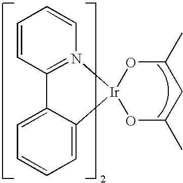
- the phosphorescent dopant material can contain a heavy metal atom, and can have a structure as shown below.
- These materials may be selected to form the doping phosphors because of their ability to tune the energies of the metal to ligand charge transfer and of the intraligand (3 ⁇ - ⁇ *) excited states.
- the heavy metals forming the described compounds are preferably Ir or Pt atoms.
- an OLED according to the invention was produced using a film of polystyrene as the inert host material.
- the dopant layers were formed by doping the inert host material with 15% of a hole transporting phosphorescent dopant and 40% of an electron transporting oxidiazole. More specifically, the phosphorescent dopants were bis(phenylpyridine) iridium acetylacetonate (PPIr), having the chemical structure:
- oxidiazole was (4-biphenyl)(4-tertbutylphenyl)oxidiazole (PDB), having the chemical structure:
- the device emitted light solely from the dopant with turn-on voltages of between about 7 and 9 Volts.
- the polystyrene acted as an inert matrix in which the dopants were supported.
- this device produced light in the green region of the visible spectrum, a different phosphor dopant in the same configuration may be used to produce light in the blue region of the spectrum.
Abstract
Description

In the diagram, M represents a heavy transition metal, C—N a cyclometallated ligand and O—X a coordination ligand wherein X can be 0, N or S, and wherein n=1 or 2, and p=0 or 1. These materials may be selected to form the doping phosphors because of their ability to tune the energies of the metal to ligand charge transfer and of the intraligand (3π-π*) excited states. In one example, the heavy metals forming the described compounds are preferably Ir or Pt atoms.

and bis(2-phenylbenzothiazole) iridium acetylacetonate (BTIr), having the chemical structure:

and the oxidiazole was (4-biphenyl)(4-tertbutylphenyl)oxidiazole (PDB), having the chemical structure:
The device emitted light solely from the dopant with turn-on voltages of between about 7 and 9 Volts. The polystyrene acted as an inert matrix in which the dopants were supported. Although this device produced light in the green region of the visible spectrum, a different phosphor dopant in the same configuration may be used to produce light in the blue region of the spectrum.
Claims (41)

Priority Applications (1)
| Application Number | Priority Date | Filing Date | Title |
|---|---|---|---|
| US10/472,401 US7294849B2 (en) | 2001-03-14 | 2002-03-13 | Materials and devices for blue phosphorescence based organic light emitting diodes |
Applications Claiming Priority (4)
| Application Number | Priority Date | Filing Date | Title |
|---|---|---|---|
| US27548101P | 2001-03-14 | 2001-03-14 | |
| US60275481 | 2001-03-14 | ||
| US10/472,401 US7294849B2 (en) | 2001-03-14 | 2002-03-13 | Materials and devices for blue phosphorescence based organic light emitting diodes |
| PCT/US2002/007492 WO2002074015A2 (en) | 2001-03-14 | 2002-03-13 | Materials and devices for blue phosphorescence based organic light emitting diodes |
Publications (2)
| Publication Number | Publication Date |
|---|---|
| US20040155238A1 US20040155238A1 (en) | 2004-08-12 |
| US7294849B2 true US7294849B2 (en) | 2007-11-13 |
Family
ID=23052471
Family Applications (1)
| Application Number | Title | Priority Date | Filing Date |
|---|---|---|---|
| US10/472,401 Expired - Lifetime US7294849B2 (en) | 2001-03-14 | 2002-03-13 | Materials and devices for blue phosphorescence based organic light emitting diodes |
Country Status (8)
| Country | Link |
|---|---|
| US (1) | US7294849B2 (en) |
| EP (2) | EP1374320B1 (en) |
| JP (2) | JP5265840B2 (en) |
| KR (1) | KR100916231B1 (en) |
| CN (1) | CN100379049C (en) |
| AU (1) | AU2002306698A1 (en) |
| TW (1) | TW540252B (en) |
| WO (1) | WO2002074015A2 (en) |
Cited By (107)
| Publication number | Priority date | Publication date | Assignee | Title |
|---|---|---|---|---|
| US20070046177A1 (en) * | 2001-06-15 | 2007-03-01 | Canon Kabushiki Kaisha | Light emitting device having dopant in a light emitting layer, and method of producing the light emitting device |
| US20090200927A1 (en) * | 2008-02-09 | 2009-08-13 | Universal Display Corporation | Organic light emitting device architecture |
| US20110057171A1 (en) * | 2006-12-28 | 2011-03-10 | Universal Display Corporation | Long lifetime Phosphorescent Organic Light Emitting Device (OLED) Structures |
| US20110177641A1 (en) * | 2010-01-20 | 2011-07-21 | Universal Display Corporation | Electroluminescent devices for lighting applications |
| US20110215309A1 (en) * | 2008-09-04 | 2011-09-08 | Universal Display Corporation | White phosphorescent organic light emitting devices |
| DE102013013876A1 (en) | 2013-08-20 | 2015-03-12 | Merck Patent Gmbh | metal complexes |
| WO2015082046A2 (en) | 2013-12-06 | 2015-06-11 | Merck Patent Gmbh | Substituted oxepines |
| EP2887417A2 (en) | 2013-12-17 | 2015-06-24 | The Regents Of The University Of Michigan | Extended OLED operational lifetime through phosphorescent dopant profile mangement |
| WO2015090504A2 (en) | 2013-12-19 | 2015-06-25 | Merck Patent Gmbh | Heterocyclic spiro compounds |
| WO2015135625A1 (en) | 2014-03-13 | 2015-09-17 | Merck Patent Gmbh | Formulations of luminescent compounds |
| WO2015165563A1 (en) | 2014-04-30 | 2015-11-05 | Merck Patent Gmbh | Materials for electronic devices |
| WO2015192941A1 (en) | 2014-06-18 | 2015-12-23 | Merck Patent Gmbh | Compositions for electronic devices |
| WO2016034262A1 (en) | 2014-09-05 | 2016-03-10 | Merck Patent Gmbh | Formulations and electronic devices |
| WO2016107663A1 (en) | 2014-12-30 | 2016-07-07 | Merck Patent Gmbh | Formulations and electronic devices |
| US9437824B2 (en) | 2008-12-17 | 2016-09-06 | Semiconductor Energy Laboratory Co., Ltd. | Light-emitting element, light emitting device, and electronic device |
| WO2016155866A1 (en) | 2015-03-30 | 2016-10-06 | Merck Patent Gmbh | Formulation of an organic functional material comprising a siloxane solvent |
| WO2016198141A1 (en) | 2015-06-12 | 2016-12-15 | Merck Patent Gmbh | Esters containing non-aromatic cycles as solvents for oled formulations |
| WO2017025166A1 (en) | 2015-08-13 | 2017-02-16 | Merck Patent Gmbh | Hexamethylindanes |
| WO2017036572A1 (en) | 2015-08-28 | 2017-03-09 | Merck Patent Gmbh | Formulation of an organic functional material comprising an epoxy group containing solvent |
| WO2017097391A1 (en) | 2015-12-10 | 2017-06-15 | Merck Patent Gmbh | Formulations containing ketones comprising non-aromatic cycles |
| WO2017102049A1 (en) | 2015-12-16 | 2017-06-22 | Merck Patent Gmbh | Formulations containing a mixture of at least two different solvents |
| WO2017102048A1 (en) | 2015-12-15 | 2017-06-22 | Merck Patent Gmbh | Esters containing aromatic groups as solvents for organic electronic formulations |
| WO2017102052A1 (en) | 2015-12-16 | 2017-06-22 | Merck Patent Gmbh | Formulations containing a solid solvent |
| WO2017140404A1 (en) | 2016-02-17 | 2017-08-24 | Merck Patent Gmbh | Formulation of an organic functional material |
| WO2017157983A1 (en) | 2016-03-17 | 2017-09-21 | Merck Patent Gmbh | Compounds with spirobifluorene-structures |
| DE102016003104A1 (en) | 2016-03-15 | 2017-09-21 | Merck Patent Gmbh | Container comprising a formulation containing at least one organic semiconductor |
| WO2017178311A1 (en) | 2016-04-11 | 2017-10-19 | Merck Patent Gmbh | Heterocyclic compounds comprising dibenzofuran and/or dibenzothiophene structures |
| WO2017216129A1 (en) | 2016-06-16 | 2017-12-21 | Merck Patent Gmbh | Formulation of an organic functional material |
| WO2017216128A1 (en) | 2016-06-17 | 2017-12-21 | Merck Patent Gmbh | Formulation of an organic functional material |
| WO2018001928A1 (en) | 2016-06-28 | 2018-01-04 | Merck Patent Gmbh | Formulation of an organic functional material |
| WO2018024719A1 (en) | 2016-08-04 | 2018-02-08 | Merck Patent Gmbh | Formulation of an organic functional material |
| WO2018050584A1 (en) | 2016-09-14 | 2018-03-22 | Merck Patent Gmbh | Compounds with spirobifluorene-structures |
| WO2018050583A1 (en) | 2016-09-14 | 2018-03-22 | Merck Patent Gmbh | Compounds with carbazole structures |
| WO2018060307A1 (en) | 2016-09-30 | 2018-04-05 | Merck Patent Gmbh | Compounds with diazadibenzofurane or diazadibenzothiophene structures |
| WO2018060218A1 (en) | 2016-09-30 | 2018-04-05 | Merck Patent Gmbh | Carbazoles with diazadibenzofurane or diazadibenzothiophene structures |
| WO2018077660A1 (en) | 2016-10-31 | 2018-05-03 | Merck Patent Gmbh | Formulation of an organic functional material |
| WO2018077662A1 (en) | 2016-10-31 | 2018-05-03 | Merck Patent Gmbh | Formulation of an organic functional material |
| WO2018087346A1 (en) | 2016-11-14 | 2018-05-17 | Merck Patent Gmbh | Compounds with an acceptor and a donor group |
| WO2018099846A1 (en) | 2016-11-30 | 2018-06-07 | Merck Patent Gmbh | Compounds having valerolactam structures |
| WO2018104195A1 (en) | 2016-12-05 | 2018-06-14 | Merck Patent Gmbh | Nitrogen-containing heterocycles for use in oleds |
| WO2018104202A1 (en) | 2016-12-06 | 2018-06-14 | Merck Patent Gmbh | Preparation process for an electronic device |
| WO2018108760A1 (en) | 2016-12-13 | 2018-06-21 | Merck Patent Gmbh | Formulation of an organic functional material |
| WO2018114883A1 (en) | 2016-12-22 | 2018-06-28 | Merck Patent Gmbh | Mixtures comprising at least two organofunctional compounds |
| WO2018138319A1 (en) | 2017-01-30 | 2018-08-02 | Merck Patent Gmbh | Method for forming an organic electroluminescence (el) element |
| WO2018138318A1 (en) | 2017-01-30 | 2018-08-02 | Merck Patent Gmbh | Method for forming an organic element of an electronic device |
| WO2018138039A1 (en) | 2017-01-25 | 2018-08-02 | Merck Patent Gmbh | Carbazole derivatives |
| WO2018166932A1 (en) | 2017-03-13 | 2018-09-20 | Merck Patent Gmbh | Compounds with arylamine structures |
| WO2018178136A1 (en) | 2017-03-31 | 2018-10-04 | Merck Patent Gmbh | Printing method for an organic light emitting diode (oled) |
| WO2018189050A1 (en) | 2017-04-10 | 2018-10-18 | Merck Patent Gmbh | Formulation of an organic functional material |
| WO2018189134A1 (en) | 2017-04-13 | 2018-10-18 | Merck Patent Gmbh | Composition for organic electronic devices |
| WO2018202603A1 (en) | 2017-05-03 | 2018-11-08 | Merck Patent Gmbh | Formulation of an organic functional material |
| WO2018215318A1 (en) | 2017-05-22 | 2018-11-29 | Merck Patent Gmbh | Hexacyclic heteroaromatic compounds for electronic devices |
| WO2019002198A1 (en) | 2017-06-26 | 2019-01-03 | Merck Patent Gmbh | Homogeneous mixtures |
| WO2019007867A1 (en) | 2017-07-05 | 2019-01-10 | Merck Patent Gmbh | Composition for organic electronic devices |
| WO2019007866A1 (en) | 2017-07-05 | 2019-01-10 | Merck Patent Gmbh | Composition for organic electronic devices |
| WO2019016184A1 (en) | 2017-07-18 | 2019-01-24 | Merck Patent Gmbh | Formulation of an organic functional material |
| WO2019096717A2 (en) | 2017-11-14 | 2019-05-23 | Merck Patent Gmbh | Composition for organic electronic devices |
| WO2019115573A1 (en) | 2017-12-15 | 2019-06-20 | Merck Patent Gmbh | Formulation of an organic functional material |
| WO2019115577A1 (en) | 2017-12-15 | 2019-06-20 | Merck Patent Gmbh | Substituted aromatic amines for use in organic electroluminescent devices |
| WO2019121458A1 (en) | 2017-12-19 | 2019-06-27 | Merck Patent Gmbh | Heterocyclic compound for use in electronic devices |
| WO2019162483A1 (en) | 2018-02-26 | 2019-08-29 | Merck Patent Gmbh | Formulation of an organic functional material |
| WO2019229011A1 (en) | 2018-05-30 | 2019-12-05 | Merck Patent Gmbh | Composition for organic electronic devices |
| WO2019238782A1 (en) | 2018-06-15 | 2019-12-19 | Merck Patent Gmbh | Formulation of an organic functional material |
| WO2020064666A1 (en) | 2018-09-27 | 2020-04-02 | Merck Patent Gmbh | Compounds that can be used in an organic electronic device as active compounds |
| WO2020064582A1 (en) | 2018-09-24 | 2020-04-02 | Merck Patent Gmbh | Method for the production of a granular material |
| WO2020064662A2 (en) | 2018-09-27 | 2020-04-02 | Merck Patent Gmbh | Method for producing sterically hindered, nitrogen-containing heteroaromatic compounds |
| EP3647393A1 (en) | 2013-07-30 | 2020-05-06 | Merck Patent GmbH | Materials for electronic devices |
| WO2020094539A1 (en) | 2018-11-05 | 2020-05-14 | Merck Patent Gmbh | Compounds that can be used in an organic electronic device |
| WO2020094538A1 (en) | 2018-11-06 | 2020-05-14 | Merck Patent Gmbh | Method for forming an organic element of an electronic device |
| WO2020099349A1 (en) | 2018-11-14 | 2020-05-22 | Merck Patent Gmbh | Compounds that can be used for producing an organic electronic device |
| WO2020169241A1 (en) | 2019-02-18 | 2020-08-27 | Merck Patent Gmbh | Composition for organic electronic devices |
| WO2020178230A1 (en) | 2019-03-04 | 2020-09-10 | Merck Patent Gmbh | Ligands for nano-sized materials |
| EP3712229A1 (en) | 2013-07-30 | 2020-09-23 | Merck Patent GmbH | Materials for electronic devices |
| WO2021052921A1 (en) | 2019-09-19 | 2021-03-25 | Merck Patent Gmbh | Mixture of two host materials, and organic electroluminescent device comprising same |
| WO2021078831A1 (en) | 2019-10-25 | 2021-04-29 | Merck Patent Gmbh | Compounds that can be used in an organic electronic device |
| WO2021089447A1 (en) | 2019-11-04 | 2021-05-14 | Merck Patent Gmbh | Organic electroluminescent apparatus |
| WO2021122868A1 (en) | 2019-12-19 | 2021-06-24 | Merck Patent Gmbh | Compounds for electronic devices |
| WO2021170522A1 (en) | 2020-02-25 | 2021-09-02 | Merck Patent Gmbh | Use of heterocyclic compounds in an organic electronic device |
| WO2021175706A1 (en) | 2020-03-02 | 2021-09-10 | Merck Patent Gmbh | Use of sulfone compounds in an organic electronic device |
| WO2021180614A1 (en) | 2020-03-11 | 2021-09-16 | Merck Patent Gmbh | Organic electroluminescent apparatus |
| WO2021180625A1 (en) | 2020-03-11 | 2021-09-16 | Merck Patent Gmbh | Organic electroluminescent apparatus |
| WO2021213918A1 (en) | 2020-04-21 | 2021-10-28 | Merck Patent Gmbh | Formulation of an organic functional material |
| EP3904361A2 (en) | 2013-10-02 | 2021-11-03 | Merck Patent GmbH | Boron containing compounds |
| WO2021239772A1 (en) | 2020-05-29 | 2021-12-02 | Merck Patent Gmbh | Organic electroluminescent apparatus |
| WO2021254984A1 (en) | 2020-06-18 | 2021-12-23 | Merck Patent Gmbh | Indenoazanaphthalenes |
| WO2021259824A1 (en) | 2020-06-23 | 2021-12-30 | Merck Patent Gmbh | Method for producing a mixture |
| WO2022063744A1 (en) | 2020-09-24 | 2022-03-31 | Merck Patent Gmbh | Organic electroluminescent device |
| WO2022090108A1 (en) | 2020-10-27 | 2022-05-05 | Merck Patent Gmbh | Organic electroluminescent device |
| WO2022122607A1 (en) | 2020-12-08 | 2022-06-16 | Merck Patent Gmbh | An ink system and a method for inkjet printing |
| EP4037000A1 (en) | 2014-07-21 | 2022-08-03 | Merck Patent GmbH | Materials for electronic devices |
| WO2022207678A1 (en) | 2021-03-30 | 2022-10-06 | Merck Patent Gmbh | Organic electroluminescent device |
| WO2022223675A1 (en) | 2021-04-23 | 2022-10-27 | Merck Patent Gmbh | Formulation of an organic functional material |
| WO2022243403A1 (en) | 2021-05-21 | 2022-11-24 | Merck Patent Gmbh | Method for the continuous purification of at least one functional material and device for the continuous purification of at least one functional material |
| WO2023052376A1 (en) | 2021-09-30 | 2023-04-06 | Merck Patent Gmbh | Organic electroluminescent apparatus |
| WO2023052377A1 (en) | 2021-09-30 | 2023-04-06 | Merck Patent Gmbh | Organic electroluminescent apparatus |
| WO2023057327A1 (en) | 2021-10-05 | 2023-04-13 | Merck Patent Gmbh | Method for forming an organic element of an electronic device |
| WO2023061998A1 (en) | 2021-10-14 | 2023-04-20 | Merck Patent Gmbh | Materials for organic electroluminescent devices |
| WO2023078812A1 (en) | 2021-11-02 | 2023-05-11 | Merck Patent Gmbh | Benzofuro[3,2-d]pyrimidino-2,4-dicarbonitril derivatives and similar compounds for organic electroluminescence devices |
| WO2023099430A1 (en) | 2021-12-02 | 2023-06-08 | Merck Patent Gmbh | Triphenylene-triazine-dibenzofuran/dibenzothiophene derivatives for organic electroluminescent devices |
| WO2023099543A1 (en) | 2021-11-30 | 2023-06-08 | Merck Patent Gmbh | Compounds having fluorene structures |
| WO2023117835A1 (en) | 2021-12-21 | 2023-06-29 | Merck Patent Gmbh | Electronic devices |
| WO2023117836A1 (en) | 2021-12-21 | 2023-06-29 | Merck Patent Gmbh | Electronic devices |
| WO2023247662A1 (en) | 2022-06-24 | 2023-12-28 | Merck Patent Gmbh | Composition for organic electronic devices |
| WO2023247663A1 (en) | 2022-06-24 | 2023-12-28 | Merck Patent Gmbh | Composition for organic electronic devices |
| WO2024038029A1 (en) | 2022-08-17 | 2024-02-22 | Merck Patent Gmbh | Materials for organic electroluminescent devices |
| WO2024038068A1 (en) | 2022-08-19 | 2024-02-22 | Merck Patent Gmbh | Materials for organic electroluminescent devices |
| US11963442B2 (en) | 2014-04-30 | 2024-04-16 | Merck Patent Gmbh | Materials for electronic devices |
Families Citing this family (127)
| Publication number | Priority date | Publication date | Assignee | Title |
|---|---|---|---|---|
| EP1374320B1 (en) * | 2001-03-14 | 2020-05-06 | The Trustees Of Princeton University | Materials and devices for blue phosphorescence based organic light emitting diodes |
| EP3333876A1 (en) * | 2001-05-16 | 2018-06-13 | The Trustees of Princeton University | High efficiency multi-color electro-phosphorescent oleds |
| JP4006266B2 (en) * | 2001-06-15 | 2007-11-14 | キヤノン株式会社 | Light emitting device and method for manufacturing light emitting device |
| WO2003101157A1 (en) | 2002-05-08 | 2003-12-04 | Zeolux Corporation | Lighting devices using feedback enhanced light emitting diode |
| US7332739B2 (en) | 2002-06-20 | 2008-02-19 | Samsung Sdi Co., Ltd. | Organic electroluminescent device using mixture of phosphorescent material as light-emitting substance |
| KR100483986B1 (en) | 2002-06-20 | 2005-04-15 | 삼성에스디아이 주식회사 | Organic polymer electroluminescent display device using phosphresecnce mixture as emiting material |
| KR101028435B1 (en) * | 2002-08-16 | 2011-04-14 | 유니버시티 오브 써던 캘리포니아 | Organic light emitting materials with anionic ligand |
| US20040062947A1 (en) * | 2002-09-25 | 2004-04-01 | Lamansky Sergey A. | Organic electroluminescent compositions |
| JP2004179142A (en) * | 2002-09-30 | 2004-06-24 | Sanyo Electric Co Ltd | Light emitting element |
| US6891326B2 (en) * | 2002-11-15 | 2005-05-10 | Universal Display Corporation | Structure and method of fabricating organic devices |
| JP4152173B2 (en) * | 2002-11-18 | 2008-09-17 | 出光興産株式会社 | Organic electroluminescence device |
| KR100520937B1 (en) * | 2002-12-03 | 2005-10-17 | 엘지전자 주식회사 | Phenyl pyridine - iridium metal complex compounds for organic electroluminescent device, process for preparing them and organic electroluminescent device using them |
| CN100384961C (en) * | 2002-12-13 | 2008-04-30 | 皇家飞利浦电子股份有限公司 | Electroluminescent device |
| US20040126617A1 (en) * | 2002-12-31 | 2004-07-01 | Eastman Kodak Company | Efficient electroluminescent device |
| JP4158562B2 (en) * | 2003-03-12 | 2008-10-01 | コニカミノルタホールディングス株式会社 | Organic electroluminescence element and display device |
| EP2062908B1 (en) | 2003-03-24 | 2016-07-13 | University of Southern California | Transition metal complexes comprising pyrazolylcarbazole ligands |
| JP2004296185A (en) * | 2003-03-26 | 2004-10-21 | Toyama Univ | Organic electroluminescent element |
| US20040209116A1 (en) * | 2003-04-21 | 2004-10-21 | Xiaofan Ren | Organic light emitting devices with wide gap host materials |
| US7029765B2 (en) | 2003-04-22 | 2006-04-18 | Universal Display Corporation | Organic light emitting devices having reduced pixel shrinkage |
| DE10333232A1 (en) * | 2003-07-21 | 2007-10-11 | Merck Patent Gmbh | Organic electroluminescent element |
| US20050025993A1 (en) * | 2003-07-25 | 2005-02-03 | Thompson Mark E. | Materials and structures for enhancing the performance of organic light emitting devices |
| US7018723B2 (en) | 2003-07-25 | 2006-03-28 | The University Of Southern California | Materials and structures for enhancing the performance of organic light emitting devices |
| JP2005054075A (en) * | 2003-08-05 | 2005-03-03 | Toyo Ink Mfg Co Ltd | Material for organic electroluminescent element, and organic electroluminescent element using the same |
| US7198730B2 (en) | 2003-08-28 | 2007-04-03 | E. I. Du Pont De Nemours And Company | Phosphorescent material |
| DE10356099A1 (en) | 2003-11-27 | 2005-07-07 | Covion Organic Semiconductors Gmbh | Organic electroluminescent element |
| DE10357315A1 (en) | 2003-12-05 | 2005-07-07 | Covion Organic Semiconductors Gmbh | Organic electroluminescent element |
| US7070867B2 (en) | 2003-12-05 | 2006-07-04 | The University Of Southern California | OLEDs having n-type doping |
| CN100490206C (en) * | 2003-12-25 | 2009-05-20 | 华南理工大学 | Organic/high molecular light emitting diode |
| DE10361385B4 (en) | 2003-12-29 | 2011-07-28 | OSRAM Opto Semiconductors GmbH, 93055 | Polymers, phosphorescent organic semiconducting emitter materials based on perarylated boranes, process for their preparation and uses thereof |
| US7045952B2 (en) | 2004-03-04 | 2006-05-16 | Universal Display Corporation | OLEDs with mixed host emissive layer |
| US7889774B2 (en) | 2004-03-05 | 2011-02-15 | The Trustees Of Princeton University | Organic polariton laser |
| EP1746094A4 (en) * | 2004-03-25 | 2009-06-10 | Hodogaya Chemical Co Ltd | Compound having oxadiazole ring structure substituted with pyridyl group, and organic electroluminescent device |
| US7582365B2 (en) | 2005-01-10 | 2009-09-01 | Universal Display Corporation | Reversibly reducible metal complexes as electron transporting materials for OLEDs |
| US7279704B2 (en) | 2004-05-18 | 2007-10-09 | The University Of Southern California | Complexes with tridentate ligands |
| US7655323B2 (en) | 2004-05-18 | 2010-02-02 | The University Of Southern California | OLEDs utilizing macrocyclic ligand systems |
| US7445855B2 (en) | 2004-05-18 | 2008-11-04 | The University Of Southern California | Cationic metal-carbene complexes |
| US7393599B2 (en) | 2004-05-18 | 2008-07-01 | The University Of Southern California | Luminescent compounds with carbene ligands |
| US7491823B2 (en) | 2004-05-18 | 2009-02-17 | The University Of Southern California | Luminescent compounds with carbene ligands |
| WO2005113704A2 (en) * | 2004-05-18 | 2005-12-01 | The University Of Southern California | Luminescent compounds with carbene ligands |
| US7598388B2 (en) | 2004-05-18 | 2009-10-06 | The University Of Southern California | Carbene containing metal complexes as OLEDs |
| US7534505B2 (en) | 2004-05-18 | 2009-05-19 | The University Of Southern California | Organometallic compounds for use in electroluminescent devices |
| US7601436B2 (en) | 2004-05-18 | 2009-10-13 | The University Of Southern California | Carbene metal complexes as OLED materials |
| KR100751316B1 (en) * | 2004-06-25 | 2007-08-22 | 삼성에스디아이 주식회사 | Organic electroluminescence display |
| JP4649676B2 (en) * | 2004-07-07 | 2011-03-16 | 独立行政法人科学技術振興機構 | Organic electroluminescence device |
| US7709100B2 (en) | 2004-07-07 | 2010-05-04 | Universal Display Corporation | Electroluminescent efficiency |
| EP3855519A3 (en) | 2004-07-07 | 2021-09-22 | Universal Display Corporation | Stable and efficient electroluminescent materials |
| US7316756B2 (en) | 2004-07-27 | 2008-01-08 | Eastman Kodak Company | Desiccant for top-emitting OLED |
| US9040170B2 (en) | 2004-09-20 | 2015-05-26 | Global Oled Technology Llc | Electroluminescent device with quinazoline complex emitter |
| JP4362461B2 (en) | 2004-11-05 | 2009-11-11 | 三星モバイルディスプレイ株式會社 | Organic electroluminescence device |
| US7776456B2 (en) | 2004-12-03 | 2010-08-17 | Universal Display Corporation | Organic light emitting devices with an emissive region having emissive and non-emissive layers and method of making |
| GB0427266D0 (en) * | 2004-12-13 | 2005-01-12 | Cambridge Display Tech Ltd | Phosphorescent OLED |
| US7597967B2 (en) * | 2004-12-17 | 2009-10-06 | Eastman Kodak Company | Phosphorescent OLEDs with exciton blocking layer |
| KR20060084733A (en) * | 2005-01-20 | 2006-07-25 | 삼성에스디아이 주식회사 | An organic electroluminescent device and a method for preparing the same |
| US7683536B2 (en) * | 2005-03-31 | 2010-03-23 | The Trustees Of Princeton University | OLEDs utilizing direct injection to the triplet state |
| US9070884B2 (en) | 2005-04-13 | 2015-06-30 | Universal Display Corporation | Hybrid OLED having phosphorescent and fluorescent emitters |
| EP1713136B1 (en) * | 2005-04-13 | 2007-12-12 | Novaled AG | Device for organic light emitting diode of pin-type and method for its manufacture |
| US7807275B2 (en) | 2005-04-21 | 2010-10-05 | Universal Display Corporation | Non-blocked phosphorescent OLEDs |
| US9051344B2 (en) | 2005-05-06 | 2015-06-09 | Universal Display Corporation | Stability OLED materials and devices |
| US7902374B2 (en) | 2005-05-06 | 2011-03-08 | Universal Display Corporation | Stability OLED materials and devices |
| US7851072B2 (en) | 2005-05-19 | 2010-12-14 | Universal Display Corporation | Stable and efficient electroluminescent materials |
| JP5095612B2 (en) | 2005-05-31 | 2012-12-12 | ユニバーサル ディスプレイ コーポレイション | Triphenylene host in phosphorescent light-emitting diodes |
| US7474048B2 (en) | 2005-06-01 | 2009-01-06 | The Trustees Of Princeton University | Fluorescent filtered electrophosphorescence |
| KR101308282B1 (en) | 2005-09-05 | 2013-09-13 | 이데미쓰 고산 가부시키가이샤 | Blue light emitting organic electroluminescence element |
| US8148891B2 (en) | 2005-10-04 | 2012-04-03 | Universal Display Corporation | Electron impeding layer for high efficiency phosphorescent OLEDs |
| US8956738B2 (en) | 2005-10-26 | 2015-02-17 | Global Oled Technology Llc | Organic element for low voltage electroluminescent devices |
| US7767317B2 (en) | 2005-10-26 | 2010-08-03 | Global Oled Technology Llc | Organic element for low voltage electroluminescent devices |
| CN1787250B (en) * | 2005-11-01 | 2012-05-02 | 友达光电股份有限公司 | Phosphorescence organic lighting assemply, display, all colour display |
| JPWO2007055186A1 (en) | 2005-11-09 | 2009-04-30 | コニカミノルタホールディングス株式会社 | Organic electroluminescence element, display device and lighting device |
| JP4878819B2 (en) * | 2005-11-18 | 2012-02-15 | ケミプロ化成株式会社 | Novel triazine derivative and organic electroluminescence device containing the same |
| US8021763B2 (en) | 2005-11-23 | 2011-09-20 | The Trustees Of Princeton University | Phosphorescent OLED with interlayer |
| US9666826B2 (en) | 2005-11-30 | 2017-05-30 | Global Oled Technology Llc | Electroluminescent device including an anthracene derivative |
| US7651791B2 (en) | 2005-12-15 | 2010-01-26 | Idemitsu Kosan Co., Ltd. | Material for organic electroluminescence device and electroluminescence device employing the same |
| CN100361983C (en) * | 2005-12-16 | 2008-01-16 | 武汉大学 | Halogen atom-containing bidentate ligand, its iridium complex and electrogenerated phosphorescence device |
| US8518556B2 (en) * | 2006-01-27 | 2013-08-27 | Konica Minolta Holdings, Inc. | Electroluminescent element |
| US8142909B2 (en) | 2006-02-10 | 2012-03-27 | Universal Display Corporation | Blue phosphorescent imidazophenanthridine materials |
| KR101634509B1 (en) | 2006-02-10 | 2016-06-28 | 유니버셜 디스플레이 코포레이션 | METAL COMPLEXES OF CYCLOMETALLATED IMIDAZO[1,2-f]PHENANTHRIDINE AND DIIMIDAZO[1,2-A:1',2'-C]QUINAZOLINE LIGANDS AND ISOELECTRONIC AND BENZANNULATED ANALOGS THEREOF |
| JP5189077B2 (en) | 2006-04-13 | 2013-04-24 | ユニバーシティ オブ サザン カリフォルニア | Organic electronic devices using phthalimide compounds |
| US8330351B2 (en) | 2006-04-20 | 2012-12-11 | Universal Display Corporation | Multiple dopant emissive layer OLEDs |
| US9118020B2 (en) | 2006-04-27 | 2015-08-25 | Global Oled Technology Llc | Electroluminescent devices including organic eil layer |
| EP2355198B1 (en) | 2006-05-08 | 2015-09-09 | Global OLED Technology LLC | OLED electron-injecting layer |
| KR100796593B1 (en) * | 2006-05-29 | 2008-01-21 | 삼성에스디아이 주식회사 | Organic Electroluminescence Display Device |
| US7579773B2 (en) | 2006-06-05 | 2009-08-25 | The Trustees Of Princeton University | Organic light-emitting device with a phosphor-sensitized fluorescent emission layer |
| US7724796B2 (en) | 2006-08-29 | 2010-05-25 | The Trustees Of Princeton University | Organic laser |
| US7710017B2 (en) | 2006-09-08 | 2010-05-04 | Universal Display Corporation | Organic light emitting device having a transparent microcavity |
| US7598381B2 (en) | 2006-09-11 | 2009-10-06 | The Trustees Of Princeton University | Near-infrared emitting organic compounds and organic devices using the same |
| US7800295B2 (en) | 2006-09-15 | 2010-09-21 | Universal Display Corporation | Organic light emitting device having a microcavity |
| US8945722B2 (en) * | 2006-10-27 | 2015-02-03 | The University Of Southern California | Materials and architectures for efficient harvesting of singlet and triplet excitons for white light emitting OLEDs |
| JP5300255B2 (en) * | 2007-02-07 | 2013-09-25 | ユー・ディー・シー アイルランド リミテッド | Organic electroluminescence device |
| US20080187748A1 (en) * | 2007-02-07 | 2008-08-07 | Masayuki Mishima | Organic electroluminescence device |
| KR101445418B1 (en) * | 2007-02-19 | 2014-09-26 | 다이니폰 인사츠 가부시키가이샤 | Organic electroluminescence element |
| US7993763B2 (en) | 2007-05-10 | 2011-08-09 | Universal Display Corporation | Organometallic compounds having host and dopant functionalities |
| JPWO2009008344A1 (en) * | 2007-07-07 | 2010-09-09 | 出光興産株式会社 | Organic EL device |
| TWI562975B (en) | 2007-08-08 | 2016-12-21 | Universal Display Corp | Single triphenylene chromophores in phosphorescent light emitting diodes |
| US8383249B2 (en) | 2007-10-04 | 2013-02-26 | Universal Display Corporation | Complexes with tridentate ligands |
| US8067100B2 (en) | 2007-10-04 | 2011-11-29 | Universal Display Corporation | Complexes with tridentate ligands |
| GB0804469D0 (en) * | 2008-03-11 | 2008-04-16 | Oled T Ltd | Compounds having electroluminescent or electron transport properties |
| DE102008039361A1 (en) | 2008-05-30 | 2009-12-03 | Osram Opto Semiconductors Gmbh | Electronic device |
| EP2313472B1 (en) | 2008-07-18 | 2012-08-15 | Basf Se | Azapyrenes for electronic applications |
| EP2161272A1 (en) | 2008-09-05 | 2010-03-10 | Basf Se | Phenanthrolines |
| KR101678235B1 (en) | 2008-09-25 | 2016-11-21 | 유니버셜 디스플레이 코포레이션 | Organoselenium materials and their uses in organic light emitting devices |
| DE102008063589A1 (en) | 2008-10-07 | 2010-04-08 | Osram Opto Semiconductors Gmbh | Radiation-emitting device |
| WO2010062643A1 (en) | 2008-10-28 | 2010-06-03 | The Regents Of The University Of Michigan | Stacked white oled having separate red, green and blue sub-elements |
| JP2010226059A (en) * | 2009-03-25 | 2010-10-07 | Toshiba Corp | Organic electroluminescent element |
| EP2443213B1 (en) | 2009-06-18 | 2014-04-23 | Basf Se | Phenanthroazole compounds as hole transporting materials for electro luminescent devices |
| US20120049168A1 (en) | 2010-08-31 | 2012-03-01 | Universal Display Corporation | Cross-Linked Charge Transport Layer Containing an Additive Compound |
| US9310766B2 (en) | 2010-09-29 | 2016-04-12 | Basf Se | Security element |
| EP2625171B1 (en) | 2010-10-07 | 2014-07-30 | Basf Se | Phenanthro[9,10-b]furans for electronic applications |
| US9079872B2 (en) | 2010-10-07 | 2015-07-14 | Basf Se | Phenanthro[9, 10-B]furans for electronic applications |
| US9385335B2 (en) * | 2011-04-05 | 2016-07-05 | Merck Patent Gmbh | Organic electroluminescent device |
| WO2012166101A1 (en) | 2011-05-27 | 2012-12-06 | Universal Display Corporation | Oled having multi-component emissivie layer |
| KR101429537B1 (en) | 2011-07-11 | 2014-08-12 | 엘지디스플레이 주식회사 | Organic light emitting diodes |
| WO2013008835A1 (en) * | 2011-07-12 | 2013-01-17 | 株式会社日立製作所 | Material for forming organic light-emitting layer, coating liquid for forming organic light-emitting element, organic light-emitting element and light source device, and method for manufacturing same |
| US9023420B2 (en) | 2011-07-14 | 2015-05-05 | Universal Display Corporation | Composite organic/inorganic layer for organic light-emitting devices |
| US8933468B2 (en) | 2012-03-16 | 2015-01-13 | Princeton University Office of Technology and Trademark Licensing | Electronic device with reduced non-device edge area |
| GB201306365D0 (en) | 2013-04-09 | 2013-05-22 | Kathirgamanathan Poopathy | Heterocyclic compounds and their use in electro-optical or opto-electronic devices |
| GB2514818B (en) * | 2013-06-05 | 2015-12-16 | Cambridge Display Tech Ltd | Polymer and organic electronic device |
| TWI526444B (en) | 2013-12-25 | 2016-03-21 | 財團法人工業技術研究院 | Organic metal compound, organic light-emitting device, and lighting device employing the same |
| KR102203774B1 (en) * | 2013-12-31 | 2021-01-18 | 엘지디스플레이 주식회사 | White Organic Emitting Device |
| WO2015134017A1 (en) | 2014-03-05 | 2015-09-11 | Universal Display Corporation | Phosphorescent oled devices |
| EP3473635B1 (en) | 2014-05-08 | 2020-07-22 | Universal Display Corporation | Stabilized imidazophenanthridine materials |
| KR102313358B1 (en) * | 2014-07-10 | 2021-10-18 | 삼성디스플레이 주식회사 | Organic light emitting device |
| KR102584846B1 (en) | 2015-05-05 | 2023-10-04 | 유니버셜 디스플레이 코포레이션 | Organic electroluminescent materials and devices |
| GB2538325A (en) * | 2015-05-15 | 2016-11-16 | Cambridge Display Tech Ltd | Organic light-emitting device |
| US10818853B2 (en) | 2015-06-04 | 2020-10-27 | University Of Southern California | Organic electroluminescent materials and devices |
| CN105679957B (en) * | 2016-04-20 | 2017-12-05 | 京东方科技集团股份有限公司 | Organic luminescent device and preparation method thereof |
| EP3492480B1 (en) | 2017-11-29 | 2021-10-20 | Universal Display Corporation | Organic electroluminescent materials and devices |
| CN110845538B (en) * | 2019-11-29 | 2023-04-07 | 武汉天马微电子有限公司 | Organic compound and application thereof |
Citations (18)
| Publication number | Priority date | Publication date | Assignee | Title |
|---|---|---|---|---|
| DE4428450A1 (en) | 1994-08-11 | 1996-02-15 | Philips Patentverwaltung | Optical electroluminescent component used as LED's |
| EP0757088A2 (en) | 1995-08-04 | 1997-02-05 | Toyo Ink Manufacturing Co., Ltd. | Organoelectroluminescence device material and organoelectroluminescence device for which the material is adapted |
| WO2001008230A1 (en) | 1999-07-21 | 2001-02-01 | The Trustees Of Princeton University | Intersystem crossing agents for efficient utilization of excitons in organic light emitting devices |
| WO2001041512A1 (en) | 1999-12-01 | 2001-06-07 | The Trustees Of Princeton University | Complexes of form l2mx as phosphorescent dopants for organic leds |
| US6285039B1 (en) * | 1996-08-19 | 2001-09-04 | Tdk Corporation | Organic electroluminescent device |
| US20020028347A1 (en) | 2000-06-12 | 2002-03-07 | Marrocco Matthew L. | Polymer matrix electroluminescent materials and devices |
| US6361886B2 (en) * | 1998-12-09 | 2002-03-26 | Eastman Kodak Company | Electroluminescent device with improved hole transport layer |
| US6365270B2 (en) | 1994-12-13 | 2002-04-02 | The Trustees Of Princeton University | Organic light emitting devices |
| US6392250B1 (en) * | 2000-06-30 | 2002-05-21 | Xerox Corporation | Organic light emitting devices having improved performance |
| US20020101154A1 (en) | 2001-02-01 | 2002-08-01 | Satoshi Seo | Organic light emitting element and display device using the element |
| US20020113545A1 (en) | 2000-12-18 | 2002-08-22 | Chihaya Adachi | Highly efficient oleds using doped ambipolar conductive molecular organic thin films |
| US6495274B1 (en) * | 1999-07-30 | 2002-12-17 | Sony Corporation | Organic electroluminescent device |
| US6579630B2 (en) * | 2000-12-07 | 2003-06-17 | Canon Kabushiki Kaisha | Deuterated semiconducting organic compounds used for opto-electronic devices |
| US6603150B2 (en) * | 2001-09-28 | 2003-08-05 | Eastman Kodak Company | Organic light-emitting diode having an interface layer between the hole-transporting layer and the light-emitting layer |
| US6720090B2 (en) * | 2001-01-02 | 2004-04-13 | Eastman Kodak Company | Organic light emitting diode devices with improved luminance efficiency |
| US6784016B2 (en) * | 2001-06-21 | 2004-08-31 | The Trustees Of Princeton University | Organic light-emitting devices with blocking and transport layers |
| US6821645B2 (en) * | 1999-12-27 | 2004-11-23 | Fuji Photo Film Co., Ltd. | Light-emitting material comprising orthometalated iridium complex, light-emitting device, high efficiency red light-emitting device, and novel iridium complex |
| US6869693B2 (en) * | 2000-10-10 | 2005-03-22 | E. I. Du Pont De Nemours And Company | Polymers having attached luminescent metal complexes and devices made with such polymers |
Family Cites Families (9)
| Publication number | Priority date | Publication date | Assignee | Title |
|---|---|---|---|---|
| WO1996005607A1 (en) * | 1994-08-11 | 1996-02-22 | Philips Electronics N.V. | Solid-stage image intensifier and x-ray examination apparatus comprising a solid-state image intensifier |
| EP0757035B1 (en) * | 1995-08-03 | 2002-12-04 | Kyocera Mita Corporation | Phenanthrylenediamine derivative and electrophotosensitive material using the same |
| GB9711237D0 (en) * | 1997-06-02 | 1997-07-23 | Isis Innovation | Organomettallic Complexes |
| DE69841006D1 (en) * | 1997-10-09 | 2009-09-03 | Univ Princeton | Phosphorescent organic light-emitting device |
| US6030715A (en) * | 1997-10-09 | 2000-02-29 | The University Of Southern California | Azlactone-related dopants in the emissive layer of an OLED |
| CN1094657C (en) * | 1998-03-10 | 2002-11-20 | 陈兴 | All colour organic luminous diode and its manufacturing method |
| JP2000348859A (en) * | 1999-06-03 | 2000-12-15 | Chisso Corp | Organic electroluminescent element |
| SG115435A1 (en) * | 2000-12-28 | 2005-10-28 | Semiconductor Energy Lab | Luminescent device |
| EP1374320B1 (en) * | 2001-03-14 | 2020-05-06 | The Trustees Of Princeton University | Materials and devices for blue phosphorescence based organic light emitting diodes |
-
2002
- 2002-03-13 EP EP02750605.4A patent/EP1374320B1/en not_active Expired - Lifetime
- 2002-03-13 JP JP2002571749A patent/JP5265840B2/en not_active Expired - Lifetime
- 2002-03-13 US US10/472,401 patent/US7294849B2/en not_active Expired - Lifetime
- 2002-03-13 KR KR1020037012019A patent/KR100916231B1/en active IP Right Grant
- 2002-03-13 CN CNB02808084XA patent/CN100379049C/en not_active Expired - Lifetime
- 2002-03-13 EP EP20100177763 patent/EP2276084A1/en not_active Ceased
- 2002-03-13 WO PCT/US2002/007492 patent/WO2002074015A2/en active Application Filing
- 2002-03-13 AU AU2002306698A patent/AU2002306698A1/en not_active Abandoned
- 2002-03-14 TW TW091104821A patent/TW540252B/en not_active IP Right Cessation
-
2009
- 2009-12-17 JP JP2009286813A patent/JP2010080979A/en not_active Withdrawn
Patent Citations (19)
| Publication number | Priority date | Publication date | Assignee | Title |
|---|---|---|---|---|
| DE4428450A1 (en) | 1994-08-11 | 1996-02-15 | Philips Patentverwaltung | Optical electroluminescent component used as LED's |
| US6365270B2 (en) | 1994-12-13 | 2002-04-02 | The Trustees Of Princeton University | Organic light emitting devices |
| EP0757088A2 (en) | 1995-08-04 | 1997-02-05 | Toyo Ink Manufacturing Co., Ltd. | Organoelectroluminescence device material and organoelectroluminescence device for which the material is adapted |
| US6285039B1 (en) * | 1996-08-19 | 2001-09-04 | Tdk Corporation | Organic electroluminescent device |
| US6361886B2 (en) * | 1998-12-09 | 2002-03-26 | Eastman Kodak Company | Electroluminescent device with improved hole transport layer |
| WO2001008230A1 (en) | 1999-07-21 | 2001-02-01 | The Trustees Of Princeton University | Intersystem crossing agents for efficient utilization of excitons in organic light emitting devices |
| US6495274B1 (en) * | 1999-07-30 | 2002-12-17 | Sony Corporation | Organic electroluminescent device |
| WO2001041512A1 (en) | 1999-12-01 | 2001-06-07 | The Trustees Of Princeton University | Complexes of form l2mx as phosphorescent dopants for organic leds |
| US6821645B2 (en) * | 1999-12-27 | 2004-11-23 | Fuji Photo Film Co., Ltd. | Light-emitting material comprising orthometalated iridium complex, light-emitting device, high efficiency red light-emitting device, and novel iridium complex |
| US20020028347A1 (en) | 2000-06-12 | 2002-03-07 | Marrocco Matthew L. | Polymer matrix electroluminescent materials and devices |
| US6392250B1 (en) * | 2000-06-30 | 2002-05-21 | Xerox Corporation | Organic light emitting devices having improved performance |
| US6869693B2 (en) * | 2000-10-10 | 2005-03-22 | E. I. Du Pont De Nemours And Company | Polymers having attached luminescent metal complexes and devices made with such polymers |
| US6579630B2 (en) * | 2000-12-07 | 2003-06-17 | Canon Kabushiki Kaisha | Deuterated semiconducting organic compounds used for opto-electronic devices |
| US20020113545A1 (en) | 2000-12-18 | 2002-08-22 | Chihaya Adachi | Highly efficient oleds using doped ambipolar conductive molecular organic thin films |
| US6573651B2 (en) * | 2000-12-18 | 2003-06-03 | The Trustees Of Princeton University | Highly efficient OLEDs using doped ambipolar conductive molecular organic thin films |
| US6720090B2 (en) * | 2001-01-02 | 2004-04-13 | Eastman Kodak Company | Organic light emitting diode devices with improved luminance efficiency |
| US20020101154A1 (en) | 2001-02-01 | 2002-08-01 | Satoshi Seo | Organic light emitting element and display device using the element |
| US6784016B2 (en) * | 2001-06-21 | 2004-08-31 | The Trustees Of Princeton University | Organic light-emitting devices with blocking and transport layers |
| US6603150B2 (en) * | 2001-09-28 | 2003-08-05 | Eastman Kodak Company | Organic light-emitting diode having an interface layer between the hole-transporting layer and the light-emitting layer |
Non-Patent Citations (9)
| Title |
|---|
| Baldo, et al., "Highly Efficient Phosphorescent Emission from Organic Electroluminescent Devices", Nature, vol. 395, pp. 151-154, Sep. 1998. |
| Baldo, et al., "Very High Efficiency Green Organic Light Emitting Devices based on Electrophosphorescence", Appl. Phys. Letter, vol. 75, No. 1, pp. 4-6 (Jul. 5, 1999). |
| C. Adachi, et al., "High-efficiency organic electrophosphorescent devices with tris(2-phenylpyridine) iridium doped into electron-transporting materials", Appl. Phys. Lett., vol. 77, No. 6, pp. 904-906, (Aug. 7, 2000). |
| C. L. Lee, et al., "Polymer phsophorescent light-emitting devices doped with tris(2-phenylpyridine) iridium as a triplet emitter", Appl. Phys. Lett., vol. 77, No. 15, pp. 2280-2282 (Oct. 9, 2000). |
| D. F. O'Brien, et al., "Improved Energy transfer in electrophosphorescent devices", Appl. Phys. Lett., vol. 74, No. 3, pp. 442-444 (Jan. 18, 1999). |
| Lyons et al., 1998, Solid-State Light-Emitting Devices Based on the Trischelated Rithenium (ll) Complex 1 Thin Film Blends with Poly(ethylene oxide), J. Am. Chem. Soc. 120:12100-12107. |
| M. J. Yang, et al., "Use of poly(9-vinylcarbazole) as Host Material for Iridium Complexes in High-Efficiency Organic Light emitting devices", Japanese J. Appl. Phys., Part 2, vol. 39, pp. L828-L829 (2000). |
| Supplementary European Search Report for European Patent Application No.: 02750605, mailed on Mar. 19, 2007. |
| T. Tsutsui, et al., "High Quantum Efficiency in Organic Light-Emitting Devices with Iridium-Complex as a Triplet Emissive Center", Japanese. J. Appl. Phys., Part 2, vol. 38, pp. L1502-L1504 (1999). |
Cited By (136)
| Publication number | Priority date | Publication date | Assignee | Title |
|---|---|---|---|---|
| US7910227B2 (en) | 2001-06-15 | 2011-03-22 | Canon Kabushiki Kaisha | Light emitting device having dopants in a light emitting layer |
| US20080265763A1 (en) * | 2001-06-15 | 2008-10-30 | Canon Kabushiki Kaisha | Light emitting device having dopants in a light emitting layer |
| US20080265762A1 (en) * | 2001-06-15 | 2008-10-30 | Canon Kabushiki Kaisha | Light emitting device having dopants in a light emitting layer |
| US20080265761A1 (en) * | 2001-06-15 | 2008-10-30 | Canon Kabushiki Kaisha | Light emitting device having dopants in a light emitting layer |
| US7446471B2 (en) | 2001-06-15 | 2008-11-04 | Canon Kabushiki Kaisha | OLED provided with organic layer comprising first and second dopants based on iridium organic complex compounds |
| US20070046177A1 (en) * | 2001-06-15 | 2007-03-01 | Canon Kabushiki Kaisha | Light emitting device having dopant in a light emitting layer, and method of producing the light emitting device |
| US7736758B2 (en) | 2001-06-15 | 2010-06-15 | Canon Kabushiki Kaisha | Light emitting device having dopants in a light emitting layer |
| US7790299B2 (en) | 2001-06-15 | 2010-09-07 | Canon Kabushiki Kaisha | Light emitting device having dopants in a light emitting layer |
| US20110089821A1 (en) * | 2001-06-15 | 2011-04-21 | Canon Kabushiki Kaisha | Light emitting device having dopants in a light emitting layer |
| US20110057171A1 (en) * | 2006-12-28 | 2011-03-10 | Universal Display Corporation | Long lifetime Phosphorescent Organic Light Emitting Device (OLED) Structures |
| US8866377B2 (en) | 2006-12-28 | 2014-10-21 | Universal Display Corporation | Long lifetime phosphorescent organic light emitting device (OLED) structures |
| US8040053B2 (en) | 2008-02-09 | 2011-10-18 | Universal Display Corporation | Organic light emitting device architecture for reducing the number of organic materials |
| US20090200927A1 (en) * | 2008-02-09 | 2009-08-13 | Universal Display Corporation | Organic light emitting device architecture |
| US20110215309A1 (en) * | 2008-09-04 | 2011-09-08 | Universal Display Corporation | White phosphorescent organic light emitting devices |
| US8513658B2 (en) | 2008-09-04 | 2013-08-20 | Universal Display Corporation | White phosphorescent organic light emitting devices |
| US9437824B2 (en) | 2008-12-17 | 2016-09-06 | Semiconductor Energy Laboratory Co., Ltd. | Light-emitting element, light emitting device, and electronic device |
| US9054344B2 (en) | 2010-01-20 | 2015-06-09 | Universal Display Corporation | Electroluminescent devices for lighting applications |
| US8288187B2 (en) | 2010-01-20 | 2012-10-16 | Universal Display Corporation | Electroluminescent devices for lighting applications |
| US20110177641A1 (en) * | 2010-01-20 | 2011-07-21 | Universal Display Corporation | Electroluminescent devices for lighting applications |
| EP3647393A1 (en) | 2013-07-30 | 2020-05-06 | Merck Patent GmbH | Materials for electronic devices |
| EP3712229A1 (en) | 2013-07-30 | 2020-09-23 | Merck Patent GmbH | Materials for electronic devices |
| DE102013013876A1 (en) | 2013-08-20 | 2015-03-12 | Merck Patent Gmbh | metal complexes |
| EP3904361A2 (en) | 2013-10-02 | 2021-11-03 | Merck Patent GmbH | Boron containing compounds |
| WO2015082046A2 (en) | 2013-12-06 | 2015-06-11 | Merck Patent Gmbh | Substituted oxepines |
| EP2887417A2 (en) | 2013-12-17 | 2015-06-24 | The Regents Of The University Of Michigan | Extended OLED operational lifetime through phosphorescent dopant profile mangement |
| EP3690972A1 (en) | 2013-12-17 | 2020-08-05 | The Regents Of The University Of Michigan | Extended oled operational lifetime through phosphorescent dopant profile management |
| EP3708634A1 (en) | 2013-12-19 | 2020-09-16 | Merck Patent GmbH | Heterocyclic spiro compounds |
| WO2015090504A2 (en) | 2013-12-19 | 2015-06-25 | Merck Patent Gmbh | Heterocyclic spiro compounds |
| US10734587B2 (en) * | 2014-03-13 | 2020-08-04 | Merck Patent Gmbh | Formulations of luminescent compounds |
| WO2015135625A1 (en) | 2014-03-13 | 2015-09-17 | Merck Patent Gmbh | Formulations of luminescent compounds |
| US11963442B2 (en) | 2014-04-30 | 2024-04-16 | Merck Patent Gmbh | Materials for electronic devices |
| US10355223B2 (en) * | 2014-04-30 | 2019-07-16 | Merck Patent Gmbh | Materials for electronic devices |
| EP3533794A2 (en) | 2014-04-30 | 2019-09-04 | Merck Patent GmbH | Materials for electronic devices |
| US10985330B2 (en) | 2014-04-30 | 2021-04-20 | Merck Patent Gmbh | Materials for electronic devices |
| WO2015165563A1 (en) | 2014-04-30 | 2015-11-05 | Merck Patent Gmbh | Materials for electronic devices |
| DE102014008722A1 (en) | 2014-06-18 | 2015-12-24 | Merck Patent Gmbh | Compositions for electronic devices |
| WO2015192941A1 (en) | 2014-06-18 | 2015-12-23 | Merck Patent Gmbh | Compositions for electronic devices |
| EP4037000A1 (en) | 2014-07-21 | 2022-08-03 | Merck Patent GmbH | Materials for electronic devices |
| WO2016034262A1 (en) | 2014-09-05 | 2016-03-10 | Merck Patent Gmbh | Formulations and electronic devices |
| WO2016107663A1 (en) | 2014-12-30 | 2016-07-07 | Merck Patent Gmbh | Formulations and electronic devices |
| WO2016155866A1 (en) | 2015-03-30 | 2016-10-06 | Merck Patent Gmbh | Formulation of an organic functional material comprising a siloxane solvent |
| WO2016198141A1 (en) | 2015-06-12 | 2016-12-15 | Merck Patent Gmbh | Esters containing non-aromatic cycles as solvents for oled formulations |
| EP3581633A1 (en) | 2015-06-12 | 2019-12-18 | Merck Patent GmbH | Esters containing non-aromatic cycles as solvents for oled formulations |
| WO2017025166A1 (en) | 2015-08-13 | 2017-02-16 | Merck Patent Gmbh | Hexamethylindanes |
| WO2017036572A1 (en) | 2015-08-28 | 2017-03-09 | Merck Patent Gmbh | Formulation of an organic functional material comprising an epoxy group containing solvent |
| WO2017097391A1 (en) | 2015-12-10 | 2017-06-15 | Merck Patent Gmbh | Formulations containing ketones comprising non-aromatic cycles |
| WO2017102048A1 (en) | 2015-12-15 | 2017-06-22 | Merck Patent Gmbh | Esters containing aromatic groups as solvents for organic electronic formulations |
| EP4084109A1 (en) | 2015-12-15 | 2022-11-02 | Merck Patent GmbH | Esters containing aromatic groups as solvents for organic electronic formulations |
| WO2017102049A1 (en) | 2015-12-16 | 2017-06-22 | Merck Patent Gmbh | Formulations containing a mixture of at least two different solvents |
| WO2017102052A1 (en) | 2015-12-16 | 2017-06-22 | Merck Patent Gmbh | Formulations containing a solid solvent |
| WO2017140404A1 (en) | 2016-02-17 | 2017-08-24 | Merck Patent Gmbh | Formulation of an organic functional material |
| DE102016003104A1 (en) | 2016-03-15 | 2017-09-21 | Merck Patent Gmbh | Container comprising a formulation containing at least one organic semiconductor |
| WO2017157783A1 (en) | 2016-03-15 | 2017-09-21 | Merck Patent Gmbh | Receptacle comprising a formulation containing at least one organic semiconductor |
| WO2017157983A1 (en) | 2016-03-17 | 2017-09-21 | Merck Patent Gmbh | Compounds with spirobifluorene-structures |
| WO2017178311A1 (en) | 2016-04-11 | 2017-10-19 | Merck Patent Gmbh | Heterocyclic compounds comprising dibenzofuran and/or dibenzothiophene structures |
| WO2017216129A1 (en) | 2016-06-16 | 2017-12-21 | Merck Patent Gmbh | Formulation of an organic functional material |
| WO2017216128A1 (en) | 2016-06-17 | 2017-12-21 | Merck Patent Gmbh | Formulation of an organic functional material |
| WO2018001928A1 (en) | 2016-06-28 | 2018-01-04 | Merck Patent Gmbh | Formulation of an organic functional material |
| WO2018024719A1 (en) | 2016-08-04 | 2018-02-08 | Merck Patent Gmbh | Formulation of an organic functional material |
| US11447464B2 (en) | 2016-09-14 | 2022-09-20 | Merck Patent Gmbh | Compounds with spirobifluorene-structures |
| WO2018050584A1 (en) | 2016-09-14 | 2018-03-22 | Merck Patent Gmbh | Compounds with spirobifluorene-structures |
| WO2018050583A1 (en) | 2016-09-14 | 2018-03-22 | Merck Patent Gmbh | Compounds with carbazole structures |
| WO2018060307A1 (en) | 2016-09-30 | 2018-04-05 | Merck Patent Gmbh | Compounds with diazadibenzofurane or diazadibenzothiophene structures |
| WO2018060218A1 (en) | 2016-09-30 | 2018-04-05 | Merck Patent Gmbh | Carbazoles with diazadibenzofurane or diazadibenzothiophene structures |
| WO2018077660A1 (en) | 2016-10-31 | 2018-05-03 | Merck Patent Gmbh | Formulation of an organic functional material |
| WO2018077662A1 (en) | 2016-10-31 | 2018-05-03 | Merck Patent Gmbh | Formulation of an organic functional material |
| EP4271163A2 (en) | 2016-11-14 | 2023-11-01 | Merck Patent GmbH | Compounds with an acceptor and a donor group |
| WO2018087346A1 (en) | 2016-11-14 | 2018-05-17 | Merck Patent Gmbh | Compounds with an acceptor and a donor group |
| WO2018099846A1 (en) | 2016-11-30 | 2018-06-07 | Merck Patent Gmbh | Compounds having valerolactam structures |
| WO2018104195A1 (en) | 2016-12-05 | 2018-06-14 | Merck Patent Gmbh | Nitrogen-containing heterocycles for use in oleds |
| EP3978491A1 (en) | 2016-12-05 | 2022-04-06 | Merck Patent GmbH | Nitrogen-containing heterocycles for use in oleds |
| WO2018104202A1 (en) | 2016-12-06 | 2018-06-14 | Merck Patent Gmbh | Preparation process for an electronic device |
| WO2018108760A1 (en) | 2016-12-13 | 2018-06-21 | Merck Patent Gmbh | Formulation of an organic functional material |
| WO2018114883A1 (en) | 2016-12-22 | 2018-06-28 | Merck Patent Gmbh | Mixtures comprising at least two organofunctional compounds |
| WO2018138039A1 (en) | 2017-01-25 | 2018-08-02 | Merck Patent Gmbh | Carbazole derivatives |
| WO2018138319A1 (en) | 2017-01-30 | 2018-08-02 | Merck Patent Gmbh | Method for forming an organic electroluminescence (el) element |
| WO2018138318A1 (en) | 2017-01-30 | 2018-08-02 | Merck Patent Gmbh | Method for forming an organic element of an electronic device |
| WO2018166932A1 (en) | 2017-03-13 | 2018-09-20 | Merck Patent Gmbh | Compounds with arylamine structures |
| WO2018178136A1 (en) | 2017-03-31 | 2018-10-04 | Merck Patent Gmbh | Printing method for an organic light emitting diode (oled) |
| WO2018189050A1 (en) | 2017-04-10 | 2018-10-18 | Merck Patent Gmbh | Formulation of an organic functional material |
| WO2018189134A1 (en) | 2017-04-13 | 2018-10-18 | Merck Patent Gmbh | Composition for organic electronic devices |
| WO2018202603A1 (en) | 2017-05-03 | 2018-11-08 | Merck Patent Gmbh | Formulation of an organic functional material |
| WO2018215318A1 (en) | 2017-05-22 | 2018-11-29 | Merck Patent Gmbh | Hexacyclic heteroaromatic compounds for electronic devices |
| WO2019002198A1 (en) | 2017-06-26 | 2019-01-03 | Merck Patent Gmbh | Homogeneous mixtures |
| WO2019007867A1 (en) | 2017-07-05 | 2019-01-10 | Merck Patent Gmbh | Composition for organic electronic devices |
| EP4186898A1 (en) | 2017-07-05 | 2023-05-31 | Merck Patent GmbH | Composition for organic electronic compounds |
| WO2019007866A1 (en) | 2017-07-05 | 2019-01-10 | Merck Patent Gmbh | Composition for organic electronic devices |
| WO2019016184A1 (en) | 2017-07-18 | 2019-01-24 | Merck Patent Gmbh | Formulation of an organic functional material |
| US11450809B2 (en) | 2017-11-14 | 2022-09-20 | Merck Patent Gmbh | Composition for organic electronic devices |
| WO2019096717A2 (en) | 2017-11-14 | 2019-05-23 | Merck Patent Gmbh | Composition for organic electronic devices |
| WO2019115573A1 (en) | 2017-12-15 | 2019-06-20 | Merck Patent Gmbh | Formulation of an organic functional material |
| WO2019115577A1 (en) | 2017-12-15 | 2019-06-20 | Merck Patent Gmbh | Substituted aromatic amines for use in organic electroluminescent devices |
| WO2019121458A1 (en) | 2017-12-19 | 2019-06-27 | Merck Patent Gmbh | Heterocyclic compound for use in electronic devices |
| WO2019162483A1 (en) | 2018-02-26 | 2019-08-29 | Merck Patent Gmbh | Formulation of an organic functional material |
| WO2019229011A1 (en) | 2018-05-30 | 2019-12-05 | Merck Patent Gmbh | Composition for organic electronic devices |
| WO2019238782A1 (en) | 2018-06-15 | 2019-12-19 | Merck Patent Gmbh | Formulation of an organic functional material |
| WO2020064582A1 (en) | 2018-09-24 | 2020-04-02 | Merck Patent Gmbh | Method for the production of a granular material |
| WO2020064666A1 (en) | 2018-09-27 | 2020-04-02 | Merck Patent Gmbh | Compounds that can be used in an organic electronic device as active compounds |
| WO2020064662A2 (en) | 2018-09-27 | 2020-04-02 | Merck Patent Gmbh | Method for producing sterically hindered, nitrogen-containing heteroaromatic compounds |
| EP4190880A1 (en) | 2018-09-27 | 2023-06-07 | Merck Patent GmbH | Compounds usable as active compounds in an organic electronic device |
| WO2020094539A1 (en) | 2018-11-05 | 2020-05-14 | Merck Patent Gmbh | Compounds that can be used in an organic electronic device |
| WO2020094538A1 (en) | 2018-11-06 | 2020-05-14 | Merck Patent Gmbh | Method for forming an organic element of an electronic device |
| WO2020099349A1 (en) | 2018-11-14 | 2020-05-22 | Merck Patent Gmbh | Compounds that can be used for producing an organic electronic device |
| WO2020169241A1 (en) | 2019-02-18 | 2020-08-27 | Merck Patent Gmbh | Composition for organic electronic devices |
| WO2020178230A1 (en) | 2019-03-04 | 2020-09-10 | Merck Patent Gmbh | Ligands for nano-sized materials |
| WO2021052921A1 (en) | 2019-09-19 | 2021-03-25 | Merck Patent Gmbh | Mixture of two host materials, and organic electroluminescent device comprising same |
| WO2021078831A1 (en) | 2019-10-25 | 2021-04-29 | Merck Patent Gmbh | Compounds that can be used in an organic electronic device |
| WO2021089447A1 (en) | 2019-11-04 | 2021-05-14 | Merck Patent Gmbh | Organic electroluminescent apparatus |
| WO2021122868A1 (en) | 2019-12-19 | 2021-06-24 | Merck Patent Gmbh | Compounds for electronic devices |
| WO2021170522A1 (en) | 2020-02-25 | 2021-09-02 | Merck Patent Gmbh | Use of heterocyclic compounds in an organic electronic device |
| WO2021175706A1 (en) | 2020-03-02 | 2021-09-10 | Merck Patent Gmbh | Use of sulfone compounds in an organic electronic device |
| WO2021180614A1 (en) | 2020-03-11 | 2021-09-16 | Merck Patent Gmbh | Organic electroluminescent apparatus |
| WO2021180625A1 (en) | 2020-03-11 | 2021-09-16 | Merck Patent Gmbh | Organic electroluminescent apparatus |
| WO2021213918A1 (en) | 2020-04-21 | 2021-10-28 | Merck Patent Gmbh | Formulation of an organic functional material |
| WO2021239772A1 (en) | 2020-05-29 | 2021-12-02 | Merck Patent Gmbh | Organic electroluminescent apparatus |
| WO2021254984A1 (en) | 2020-06-18 | 2021-12-23 | Merck Patent Gmbh | Indenoazanaphthalenes |
| WO2021259824A1 (en) | 2020-06-23 | 2021-12-30 | Merck Patent Gmbh | Method for producing a mixture |
| WO2022063744A1 (en) | 2020-09-24 | 2022-03-31 | Merck Patent Gmbh | Organic electroluminescent device |
| WO2022090108A1 (en) | 2020-10-27 | 2022-05-05 | Merck Patent Gmbh | Organic electroluminescent device |
| WO2022122607A1 (en) | 2020-12-08 | 2022-06-16 | Merck Patent Gmbh | An ink system and a method for inkjet printing |
| WO2022207678A1 (en) | 2021-03-30 | 2022-10-06 | Merck Patent Gmbh | Organic electroluminescent device |
| WO2022223675A1 (en) | 2021-04-23 | 2022-10-27 | Merck Patent Gmbh | Formulation of an organic functional material |
| WO2022243403A1 (en) | 2021-05-21 | 2022-11-24 | Merck Patent Gmbh | Method for the continuous purification of at least one functional material and device for the continuous purification of at least one functional material |
| WO2023052376A1 (en) | 2021-09-30 | 2023-04-06 | Merck Patent Gmbh | Organic electroluminescent apparatus |
| WO2023052377A1 (en) | 2021-09-30 | 2023-04-06 | Merck Patent Gmbh | Organic electroluminescent apparatus |
| WO2023057327A1 (en) | 2021-10-05 | 2023-04-13 | Merck Patent Gmbh | Method for forming an organic element of an electronic device |
| WO2023061998A1 (en) | 2021-10-14 | 2023-04-20 | Merck Patent Gmbh | Materials for organic electroluminescent devices |
| WO2023078812A1 (en) | 2021-11-02 | 2023-05-11 | Merck Patent Gmbh | Benzofuro[3,2-d]pyrimidino-2,4-dicarbonitril derivatives and similar compounds for organic electroluminescence devices |
| WO2023099543A1 (en) | 2021-11-30 | 2023-06-08 | Merck Patent Gmbh | Compounds having fluorene structures |
| WO2023099430A1 (en) | 2021-12-02 | 2023-06-08 | Merck Patent Gmbh | Triphenylene-triazine-dibenzofuran/dibenzothiophene derivatives for organic electroluminescent devices |
| WO2023117835A1 (en) | 2021-12-21 | 2023-06-29 | Merck Patent Gmbh | Electronic devices |
| WO2023117836A1 (en) | 2021-12-21 | 2023-06-29 | Merck Patent Gmbh | Electronic devices |
| WO2023247662A1 (en) | 2022-06-24 | 2023-12-28 | Merck Patent Gmbh | Composition for organic electronic devices |
| WO2023247663A1 (en) | 2022-06-24 | 2023-12-28 | Merck Patent Gmbh | Composition for organic electronic devices |
| WO2024038029A1 (en) | 2022-08-17 | 2024-02-22 | Merck Patent Gmbh | Materials for organic electroluminescent devices |
| WO2024038068A1 (en) | 2022-08-19 | 2024-02-22 | Merck Patent Gmbh | Materials for organic electroluminescent devices |
Also Published As
| Publication number | Publication date |
|---|---|
| JP2010080979A (en) | 2010-04-08 |
| EP1374320A4 (en) | 2007-04-18 |
| CN100379049C (en) | 2008-04-02 |
| WO2002074015A3 (en) | 2002-11-21 |
| US20040155238A1 (en) | 2004-08-12 |
| WO2002074015A2 (en) | 2002-09-19 |
| JP2004526284A (en) | 2004-08-26 |
| AU2002306698A1 (en) | 2002-09-24 |
| CN1535483A (en) | 2004-10-06 |
| KR20030093242A (en) | 2003-12-06 |
| EP1374320A2 (en) | 2004-01-02 |
| TW540252B (en) | 2003-07-01 |
| EP1374320B1 (en) | 2020-05-06 |
| EP2276084A1 (en) | 2011-01-19 |
| KR100916231B1 (en) | 2009-09-08 |
| JP5265840B2 (en) | 2013-08-14 |
Similar Documents
| Publication | Publication Date | Title |
|---|---|---|
| US7294849B2 (en) | Materials and devices for blue phosphorescence based organic light emitting diodes | |
| US6900588B2 (en) | Highly efficient OLEDs using doped ambipolar conductive molecular organic thin films | |
| US7285907B2 (en) | High efficiency multi-color electro-phosphorescent OLEDs | |
| US6867538B2 (en) | Double doped-layer, phosphorescent organic light emitting devices | |
| JP5328402B2 (en) | Highly stable and efficient organic light-emitting device having a mixed layer structure with phosphorescent doping | |
| JP2004515895A5 (en) |
Legal Events
| Date | Code | Title | Description |
|---|---|---|---|
| AS | Assignment |
Owner name: UNIVERSITY OF SOUTHERN CALIFORNIA, THE, CALIFORNIA Free format text: ASSIGNMENT OF ASSIGNORS INTEREST;ASSIGNOR:THOMPSON, MARK E.;REEL/FRAME:015172/0174 Effective date: 20040225 |
|
| AS | Assignment |
Owner name: TRUSTEES OF PRINCETON UNIVERSITY, THE, NEW JERSEY Free format text: ASSIGNMENT OF ASSIGNORS INTEREST;ASSIGNOR:FORREST, STEPHEN R.;REEL/FRAME:015199/0453 Effective date: 20040331 |
|
| STCF | Information on status: patent grant |
Free format text: PATENTED CASE |
|
| FPAY | Fee payment |
Year of fee payment: 4 |
|
| FEPP | Fee payment procedure |
Free format text: PAYOR NUMBER ASSIGNED (ORIGINAL EVENT CODE: ASPN); ENTITY STATUS OF PATENT OWNER: LARGE ENTITY |
|
| FPAY | Fee payment |
Year of fee payment: 8 |
|
| AS | Assignment |
Owner name: NATIONAL SCIENCE FOUNDATION, VIRGINIA Free format text: CONFIRMATORY LICENSE;ASSIGNOR:PRINCETON UNIVERSITY;REEL/FRAME:039910/0018 Effective date: 20160628 |
|
| MAFP | Maintenance fee payment |
Free format text: PAYMENT OF MAINTENANCE FEE, 12TH YEAR, LARGE ENTITY (ORIGINAL EVENT CODE: M1553); ENTITY STATUS OF PATENT OWNER: LARGE ENTITY Year of fee payment: 12 |