US7308470B2 - Smaller and lower power static mux circuitry in generating multiplier partial product signals - Google Patents
Smaller and lower power static mux circuitry in generating multiplier partial product signals Download PDFInfo
- Publication number
- US7308470B2 US7308470B2 US10/728,395 US72839503A US7308470B2 US 7308470 B2 US7308470 B2 US 7308470B2 US 72839503 A US72839503 A US 72839503A US 7308470 B2 US7308470 B2 US 7308470B2
- Authority
- US
- United States
- Prior art keywords
- circuit
- multiplier
- bit
- gate
- booth
- Prior art date
- Legal status (The legal status is an assumption and is not a legal conclusion. Google has not performed a legal analysis and makes no representation as to the accuracy of the status listed.)
- Active, expires
Links
Images


Classifications
-
- G—PHYSICS
- G06—COMPUTING; CALCULATING OR COUNTING
- G06F—ELECTRIC DIGITAL DATA PROCESSING
- G06F7/00—Methods or arrangements for processing data by operating upon the order or content of the data handled
- G06F7/38—Methods or arrangements for performing computations using exclusively denominational number representation, e.g. using binary, ternary, decimal representation
- G06F7/48—Methods or arrangements for performing computations using exclusively denominational number representation, e.g. using binary, ternary, decimal representation using non-contact-making devices, e.g. tube, solid state device; using unspecified devices
- G06F7/52—Multiplying; Dividing
- G06F7/523—Multiplying only
- G06F7/533—Reduction of the number of iteration steps or stages, e.g. using the Booth algorithm, log-sum, odd-even
- G06F7/5334—Reduction of the number of iteration steps or stages, e.g. using the Booth algorithm, log-sum, odd-even by using multiple bit scanning, i.e. by decoding groups of successive multiplier bits in order to select an appropriate precalculated multiple of the multiplicand as a partial product
- G06F7/5336—Reduction of the number of iteration steps or stages, e.g. using the Booth algorithm, log-sum, odd-even by using multiple bit scanning, i.e. by decoding groups of successive multiplier bits in order to select an appropriate precalculated multiple of the multiplicand as a partial product overlapped, i.e. with successive bitgroups sharing one or more bits being recoded into signed digit representation, e.g. using the Modified Booth Algorithm
Definitions
- This method of multiplying is slow and there have been methods developed to speed up the multiplying process.
- One method to speed up multiplying is to use radix-four multiplication or Booth multiplication. Instead of shifting and adding for every column of the multiplier, the method uses every other column.
- Booth encoding involves looking at three consecutive bits of a multiplier to determine whether to multiply the multiplicand by ⁇ 1, +1, ⁇ 2, +2, or zero to obtain a partial product. This method reduces the number of partial products to be added by one-half, and consequently reduces the complexity and power consumption of circuits that implement the method.
- the Booth encoding process consists of looking at three bits of a multiplier to determine how to calculate a partial product.
- the hexadecimal number 4E2 is shown below. 010011100010 — In long multiplication by the shift and add method, twelve partial products would be used to determine the final product.
- the number is grouped into the three-bit blocks.
- the least significant block begins with only the two least significant bits of the multiplier and zero is used as the least significant bit (LSB) of the block. Grouping starts at the LSB and each block overlaps the previous block by one bit. The most significant block is sign extended if necessary to fill out a block.
- the multiplicand is multiplied by ⁇ 1, +1, ⁇ 2, +2, or 0 to obtain the partial product.
- Table 1 shows the encoding used for each possible three-bit block.
- Booth multiplication can still result in complex circuits.
- computers that want to obtain the result of a multiply as quickly as possible use a circuit to calculate each bit of the partial products. So, for example, a 64-bit by 64-bit multiply that uses the shift and add method needs to add 64 partial products of 64 bits each; or 4096 circuits.
- a 64-bit by 64-bit multiply that uses Booth encoding reduces the number of partial products to be added by one-half. However, this method still requires adding 32 partial products of 64 bits each; or 2048 circuits.
- FIG. 1 is a block diagram of an embodiment of a circuit to generate one partial product for a Booth multiply.
- FIG. 2 is one embodiment of a multiplexer circuit for generating a partial product for multiplying using Booth encoding.
- FIG. 3 shows one embodiment of a Booth encoder circuit.
- FIG. 4 shows another embodiment of a Booth encoder circuit.
- FIG. 5 is an illustration of a partial product array circuit.
- FIG. 6 is a block diagram of one embodiment of a multiply circuit that uses a partial product array circuit.
- FIG. 7 is an illustration of one embodiment of a multiplexer circuit with increased fanout capability.
- FIG. 8 is a block diagram of one embodiment of a multiply circuit that uses a partial product circuit with an accumulator.
- FIG. 9 shows one embodiment of a method of multiplying a multiplicand and a multiplier.
- FIG. 10 shows a computer system that includes a multiply circuit.
- the partial products are generated for a type of multiplication known as radix-four multiplication, or Booth multiplication.
- FIG. 1 is a block diagram of an embodiment of a circuit 100 to generate one partial product for a Booth multiply.
- Inputs to the partial product circuit 100 are bits of the multiplicand 105 , their complements, bits of the multiplier 110 and their complements.
- the circuit 100 includes multiplexers 115 . There is one multiplexer 115 for each bit of the multiplicand 105 .
- the multiplier bits 110 are encoded using Booth encoder circuit 120 to generate Booth control signals 125 .
- the Booth control signals 125 are distributed to multiplexers 115 to select outputs to generate bits of the partial product 130 .
- the Booth control signals 125 include signals to generate a negative result (NEG), a positive result (POS), a multiply by one (M 1 ) and a multiply by two (M 2 ).
- FIG. 2 is one embodiment of a multiplexer circuit 215 .
- the circuit includes four pass gates 210 , 220 , 230 , 240 .
- the pass gates 210 , 220 , 230 , 240 are shown implemented with field effect transistors (FETs).
- FETs field effect transistors
- the FETs shown are N-type, but the multiplexer circuit 215 can also be implemented with P-type transistors or with bipolar transistors.
- the gate of the first transistor 210 is coupled to receive a multiplicand bit Z j and the gate of the second transistor 220 is coupled to receive the complement to the multiplicand bit.
- the drains of the transistors 210 , 220 are coupled together to provide an output Z j+1 ′.
- the source of the first transistor 210 is coupled to the POS control signal.
- the source of the second transistor 220 is coupled to the NEG control signal. Because only one of Z j ′ or its complement is active at any one time, the two transistors implement the truth table below in Table 2. In the table, “1” denotes an active state such as high, “0” denotes an inactive state such as low, and “X” denotes a don't care state. Although the description above uses specific source and drain connections, one of ordinary skill in the art would understand the source and drain regions are interchangeable.
- the middle two rows of the table show that the multiplicand bit is inverted at the Z j+1 ′ output by an active NEG signal or an inactive POS signal. It is also shown that if the NEG and POS control signals are both inactive, the Z j+1 ′ output is necessarily “0.”
- FIG. 2 also shows that the intermediate output Z j+1 ′ is provided to a next higher order multiplexer stage.
- the drains of the third and fourth transistors 230 , 240 are also tied together. If the control signal M 1 is active, the third transistor 230 passes the Z j+1 ′ drain output to the multiplexer output, PP j , to effect a multiply by one of the Z j+1 ′ drain output.
- the fourth transistor 240 passes the Z j ⁇ 1 ′ intermediate output from the next lower multiplexer stage to the output to effect a left shift for the multiply by two.
- Z j ⁇ 1 ′ corresponds to Z j+1 ′ from the next lower stage.
- the multiplexer output, PP j corresponds to one bit of the resultant partial product.
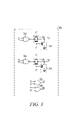
- FIG. 3 shows one embodiment 320 of a Booth encoder circuit.
- the circuit 320 uses logic circuits to encode a three-bit block of a multiplier, y 3 , y 2 , y 1 into four control signals NEG, POS, M 1 and M 2 corresponding to a negative result, a positive result, multiply by one and multiply by two.
- the Booth encoder circuit 320 is used to encode any block of three bits of the multiplier block. Although specific embodiments are discussed concerning the Booth encoder circuit 320 , one skilled in the art of logic circuit design would understand from reading this description that similar logic circuits to produce the indicated control signals are within the scope of this document.
- the embodiment 320 shows four logic circuits.
- the first logic circuit generates the NEG signal.
- the first logic circuit includes a two-input NAND gate 325 where the inputs to the NAND gate 325 are first and second bits y 2 , y 1 of the multiplier block.
- the first logic circuit also includes a transmission gate, or T-gate, 330 coupled to the output of the NAND gate 325 .
- a third multiplier bit y 3 and its complement activate the T-gate 330 .
- a pull-down transistor 335 is coupled to the output of the T-gate 330 .
- the complement of the third multiplier y 3 bit activates the pull down transistor 335 .
- the output of the T-gate 330 provides the NEG signal.
- a second logic circuit generates the POS signal.
- the second logic circuit includes a two-input NAND gate 340 , where the inputs to the NAND gate 340 are complements of the first and second bits y 2 , y 1 of the multiplier block.
- a T-gate 345 is coupled to the output of the NAND gate 340 .
- the third multiplier bit y 3 and a complement of the third multiplier bit activate the T-gate 345 .
- the output of the T-gate 345 provides the POS signal.
- a pull-down transistor 350 is coupled to the output T-gate 345 .
- the third multiplier bit y 3 activates the pull down transistor 350 .
- a third logic circuit generates the M 1 signal.
- the third logic circuit includes a two-input XOR gate 355 , where the inputs to the XOR gate 355 are first and second bits y 2 , y 1 of a multiplier block and the output of the XOR gate 355 is the M 1 signal.
- a fourth logic circuit generates the M 2 signal.
- the fourth logic includes a two-input XNOR gate 360 , where the inputs to the XNOR gate 360 are first and second bits y 2 , y 1 of a multiplier block and the output of the XNOR gate 360 is M 2 signal.
- FIG. 4 shows another embodiment 420 of a Booth encoder circuit.
- the embodiment 420 includes four logic circuits 425 , 435 , 355 , 360 to encode the NEG, POS, M 1 and M 2 signals and includes a fifth logic circuit 430 that detects when the three bits y 3 , y 2 , y 1 of the multiplier block are not ones or all zeros.
- the first logic circuit includes a two-input AND gate 425 .
- One input to the AND gate 425 is the output of the fifth logic circuit 430 and a second input is the third bit y 3 of a multiplier block.
- the output of the AND gate 425 provides the NEG signal.
- the second logic circuit includes a two-input AND gate 435 .
- One input to the AND gate 435 is the output of the fifth logic circuit 430 and a second input is the complement of the third bit y 3 of a multiplier block.
- the output of the AND gate 435 provides the POS signal.
- the third and fourth logic circuits include the XOR gate 355 to provide the M 1 signal and the XNOR gate 360 to provide the M 2 signal as discussed previously in FIG. 3 .
- FIG. 5 is an illustration of a partial product array circuit 500 .
- the circuit 500 includes a partial product circuit 100 for each partial product required by the multiply operation.
- Each partial product circuit 100 includes one Booth encoder circuit 120 to encode three-bits of a multiplier block and N multiplexer circuits for each bit of the multiplicand 105 .
- the number of partial product circuits 100 used in the array 500 is equal to one-half the number of bits in the multiplier 110 .
- the multiply operation requires multiplying an M-bit multiplier 110 by an N-bit multiplicand 105
- the number of partial product circuits 100 is M/2.
- the number of multiplexer circuits required is equal to M/2 times N.
- the letters M and N represent an integer number of bits useful in multiply circuits. Some examples include sixteen, thirty-two and sixty-four.
- a multiplying operation where M and N are relatively large integers shows the advantages of a multiplexer circuit that minimizes the number of pass gates in a multiplexer. For example, an integrated circuit implementation of a multiply operation that uses a sixty-four bit multiplier and a sixty-four multiplicand would require 32*64 or 2048 multiplexers. Use of the four-transistor multiplexer 215 of FIG. 2 over a multiplexer that uses five transistors would save 2048 transistors on the integrated circuit.
- FIG. 6 is a block diagram of one embodiment of a multiply circuit 600 that uses a partial product array circuit 500 .
- the partial product array circuit 500 receives the bits of the multiplicand and the multiplier and generates the partial products.
- An adder circuit 610 receives the partial products and them together along with generating any carries to form the final product.
- FIG. 7 is an illustration of one embodiment 700 of a multiplexer circuit 715 with increased fanout capability.
- the NEG and POS signals are inverted at the output of the Booth encoder circuit 120 using inverting buffers 750 .
- the partial product output of the multiplexer circuit 715 is also inverted using inverting buffer 760 thus preserving the logic sense of the partial product output.
- the buffers are non-inverting.
- FIG. 8 is a block diagram of one embodiment of a multiply circuit 800 that uses a partial product circuit 100 with an accumulator 810 .
- the partial products are calculated one at a time and the intermediate results are stored in the accumulator 810 .
- the partial product circuit 100 receives the bits of the multiplicand.
- a shift register 820 receives the bits of the multiplier and applies three bits of the multiplier at a time to the Booth encoder circuit 120 .
- the partial product is then shifted if necessary and added to the accumulator 810 using the arithmetic logic unit (ALU) 830 .
- the result is stored back into the accumulator 810 .
- the accumulator 810 holds the final product after all of the partial products are calculated and added to the accumulator 810 .
- FIG. 9 is an embodiment of a method 900 of multiplying multiplicand and a multiplier.
- four control signals are generated to implement Booth encoding functions of negative, positive, zero, multiply by one and multiply by two, from bits of a multiplier.
- bits of a multiplicand are multiplexed in accordance with the control signal functions to generate partial products.
- the multiplexing includes interconnecting intermediate stages of multiplexers from lower order bit positions to next higher order positions.
- the partial products are added to obtain the final product.
- FIG. 10 is a block diagram of one embodiment of a computer system 1000 that uses a partial product circuit 100 .
- the computer system includes a system bus 1010 for communicating information and a processor 1015 for processing information.
- the processor 1015 includes a multiplier circuit 1020 that includes a partial product circuit 100 for calculating partial products of a multiply operation.
- a cache memory 1030 is coupled to the processor 1015 for storing information frequently used by the processor 1015
- a main memory 1035 is coupled to the processor 1015 including random access memory (RAM) for storing information and instructions, including multiply instructions, for the processor 1015 .
- RAM random access memory
- a read only memory (ROM) 1045 or other non-volatile storage device for storing fixed information for the processor 1015 is coupled to the system bus 1010 .
- Other components such as a mass storage device 1040 , a display device 1050 , a keyboard 1055 or other input device and a cursor control device 1060 may also be included in the computer system 1000 .
Abstract
Description
010011100010—
In long multiplication by the shift and add method, twelve partial products would be used to determine the final product. To determine the partial products for Booth encoding, the number is grouped into the three-bit blocks. The least significant block begins with only the two least significant bits of the multiplier and zero is used as the least significant bit (LSB) of the block. Grouping starts at the LSB and each block overlaps the previous block by one bit. The most significant block is sign extended if necessary to fill out a block. Based on the three bits in the block, the multiplicand is multiplied by −1, +1, −2, +2, or 0 to obtain the partial product. Table 1 shows the encoding used for each possible three-bit block.
| TABLE 1 | |
| Bit Block | Partial product |
| 000 | 0 * Multiplicand |
| 001 | +1 * Multiplicand |
| 010 | +1 * Multiplicand |
| 011 | +2 * Multiplicand |
| 100 | −2 * Multiplicand |
| 101 | −1 * Multiplicand |
| 110 | −1 * Multiplicand |
| 111 | 0 * Multiplicand |
Starting with the LSB in the example above, the six blocks are 100, 001, 100, 111, 001 and 010. The multiplicand is then multiplied by −2, +1, −2, 0, +1 and +1 to obtain the six partial products. The partial products are shifted according to which block is decoded and then added together to obtain the final product.
| TABLE 2 | |||||
| Zj | NEG | POS | Zj+1′ | ||
| 0 | 0 | |
0 | ||
| 0 | 1 | |
1 | ||
| 1 | |
0 | 0 | ||
| 1 | |
1 | 1 | ||
Claims (25)
Priority Applications (1)
| Application Number | Priority Date | Filing Date | Title |
|---|---|---|---|
| US10/728,395 US7308470B2 (en) | 2003-12-05 | 2003-12-05 | Smaller and lower power static mux circuitry in generating multiplier partial product signals |
Applications Claiming Priority (1)
| Application Number | Priority Date | Filing Date | Title |
|---|---|---|---|
| US10/728,395 US7308470B2 (en) | 2003-12-05 | 2003-12-05 | Smaller and lower power static mux circuitry in generating multiplier partial product signals |
Publications (2)
| Publication Number | Publication Date |
|---|---|
| US20050125478A1 US20050125478A1 (en) | 2005-06-09 |
| US7308470B2 true US7308470B2 (en) | 2007-12-11 |
Family
ID=34633701
Family Applications (1)
| Application Number | Title | Priority Date | Filing Date |
|---|---|---|---|
| US10/728,395 Active 2025-09-02 US7308470B2 (en) | 2003-12-05 | 2003-12-05 | Smaller and lower power static mux circuitry in generating multiplier partial product signals |
Country Status (1)
| Country | Link |
|---|---|
| US (1) | US7308470B2 (en) |
Cited By (2)
| Publication number | Priority date | Publication date | Assignee | Title |
|---|---|---|---|---|
| US20050182814A1 (en) * | 2004-02-13 | 2005-08-18 | Young-Chul Rhee | Encoder for a multiplier |
| US9653165B2 (en) * | 2015-03-31 | 2017-05-16 | Xilinx, Inc. | Multiplexer-based ternary content addressable memory |
Families Citing this family (21)
| Publication number | Priority date | Publication date | Assignee | Title |
|---|---|---|---|---|
| US7425841B2 (en) | 2004-02-14 | 2008-09-16 | Tabula Inc. | Configurable circuits, IC's, and systems |
| US7167025B1 (en) * | 2004-02-14 | 2007-01-23 | Herman Schmit | Non-sequentially configurable IC |
| US20060093675A1 (en) * | 2004-10-29 | 2006-05-04 | Mathew Ebmeier | Intravaginal treatment of vaginal infections with metronidazole compositions |
| US7317331B2 (en) | 2004-11-08 | 2008-01-08 | Tabula, Inc. | Reconfigurable IC that has sections running at different reconfiguration rates |
| US7330050B2 (en) | 2004-11-08 | 2008-02-12 | Tabula, Inc. | Storage elements for a configurable IC and method and apparatus for accessing data stored in the storage elements |
| US7743085B2 (en) * | 2004-11-08 | 2010-06-22 | Tabula, Inc. | Configurable IC with large carry chains |
| US7236009B1 (en) | 2004-12-01 | 2007-06-26 | Andre Rohe | Operational time extension |
| US7310003B2 (en) * | 2005-03-15 | 2007-12-18 | Tabula, Inc. | Configurable IC with interconnect circuits that have select lines driven by user signals |
| US7530033B2 (en) | 2005-03-15 | 2009-05-05 | Tabula, Inc. | Method and apparatus for decomposing functions in a configurable IC |
| US7372297B1 (en) | 2005-11-07 | 2008-05-13 | Tabula Inc. | Hybrid interconnect/logic circuits enabling efficient replication of a function in several sub-cycles to save logic and routing resources |
| US8463836B1 (en) | 2005-11-07 | 2013-06-11 | Tabula, Inc. | Performing mathematical and logical operations in multiple sub-cycles |
| US7679401B1 (en) * | 2005-12-01 | 2010-03-16 | Tabula, Inc. | User registers implemented with routing circuits in a configurable IC |
| US7694083B1 (en) * | 2006-03-08 | 2010-04-06 | Tabula, Inc. | System and method for providing a virtual memory architecture narrower and deeper than a physical memory architecture |
| US7797497B1 (en) * | 2006-03-08 | 2010-09-14 | Tabula, Inc. | System and method for providing more logical memory ports than physical memory ports |
| US7930666B1 (en) | 2006-12-12 | 2011-04-19 | Tabula, Inc. | System and method of providing a memory hierarchy |
| US7525344B2 (en) | 2007-03-20 | 2009-04-28 | Tabula, Inc. | Configurable IC having a routing fabric with storage elements |
| US7610566B1 (en) * | 2007-03-22 | 2009-10-27 | Tabula, Inc. | Method and apparatus for function decomposition |
| WO2009035586A1 (en) | 2007-09-06 | 2009-03-19 | Tabula, Inc. | Configuration context switcher |
| US8863067B1 (en) | 2008-02-06 | 2014-10-14 | Tabula, Inc. | Sequential delay analysis by placement engines |
| JP4988627B2 (en) * | 2008-03-05 | 2012-08-01 | ルネサスエレクトロニクス株式会社 | Filter calculator and motion compensation device |
| US8166435B2 (en) * | 2008-06-26 | 2012-04-24 | Tabula, Inc. | Timing operations in an IC with configurable circuits |
Citations (20)
| Publication number | Priority date | Publication date | Assignee | Title |
|---|---|---|---|---|
| US5818743A (en) | 1995-04-21 | 1998-10-06 | Texas Instruments Incorporated | Low power multiplier |
| US5880985A (en) | 1996-10-18 | 1999-03-09 | Intel Corporation | Efficient combined array for 2n bit n bit multiplications |
| US5917741A (en) | 1996-08-29 | 1999-06-29 | Intel Corporation | Method and apparatus for performing floating-point rounding operations for multiple precisions using incrementers |
| US5943250A (en) * | 1996-10-21 | 1999-08-24 | Samsung Electronics Co., Ltd. | Parallel multiplier that supports multiple numbers with different bit lengths |
| US6035318A (en) | 1998-03-31 | 2000-03-07 | Intel Corporation | Booth multiplier for handling variable width operands |
| US6035316A (en) | 1995-08-31 | 2000-03-07 | Intel Corporation | Apparatus for performing multiply-add operations on packed data |
| US6055555A (en) | 1997-12-29 | 2000-04-25 | Intel Corporation | Interface for performing parallel arithmetic and round operations |
| US6065032A (en) * | 1998-02-19 | 2000-05-16 | Lucent Technologies Inc. | Low power multiplier for CPU and DSP |
| US6173304B1 (en) | 1998-08-20 | 2001-01-09 | Lucent Technologies, Inc. | Joint optimization of modified-booth encoder and partial product generator |
| US6240438B1 (en) * | 1996-08-29 | 2001-05-29 | Fujitsu Limited | Multiplier circuit for reducing the number of necessary elements without sacrificing high speed capability |
| US6269384B1 (en) | 1998-03-27 | 2001-07-31 | Advanced Micro Devices, Inc. | Method and apparatus for rounding and normalizing results within a multiplier |
| US6286023B1 (en) | 1998-06-19 | 2001-09-04 | Ati International Srl | Partitioned adder tree supported by a multiplexer configuration |
| US6301599B1 (en) | 1999-03-29 | 2001-10-09 | Sony Corporation Of Japan | Multiplier circuit having an optimized booth encoder/selector |
| US6308195B1 (en) | 1998-08-10 | 2001-10-23 | Mitsubishi Denki Kabushiki Kaisha | 4-2 compressor circuit and voltage holding circuit for use in 4-2 compressor circuit |
| US6393454B1 (en) * | 1995-01-30 | 2002-05-21 | Cirrus Logic, Inc. | Booth multiplier with low power, high performance input circuitry |
| US6460065B1 (en) | 1998-09-22 | 2002-10-01 | Ati International Srl | Circuit and method for partial product bit shifting |
| US20030158880A1 (en) | 2002-02-13 | 2003-08-21 | Ng Kenneth Y. | Booth encoder and partial products circuit |
| US6684236B1 (en) | 2000-02-15 | 2004-01-27 | Conexant Systems, Inc. | System of and method for efficiently performing computations through extended booth encoding of the operands thereto |
| US7069290B2 (en) * | 2002-05-06 | 2006-06-27 | Lucent Technologies Inc. | Power efficient booth recoded multiplier and method of multiplication |
| US7096246B2 (en) * | 2000-08-01 | 2006-08-22 | Stmicroelectronics S.A. | Arithmetic unit for multiplying a first quantity X by a second quantity Y |
-
2003
- 2003-12-05 US US10/728,395 patent/US7308470B2/en active Active
Patent Citations (23)
| Publication number | Priority date | Publication date | Assignee | Title |
|---|---|---|---|---|
| US6393454B1 (en) * | 1995-01-30 | 2002-05-21 | Cirrus Logic, Inc. | Booth multiplier with low power, high performance input circuitry |
| US5818743A (en) | 1995-04-21 | 1998-10-06 | Texas Instruments Incorporated | Low power multiplier |
| US6721774B1 (en) | 1995-04-21 | 2004-04-13 | Texas Instruments Incorporated | Low power multiplier |
| US6035316A (en) | 1995-08-31 | 2000-03-07 | Intel Corporation | Apparatus for performing multiply-add operations on packed data |
| US6535902B2 (en) | 1996-08-29 | 2003-03-18 | Fujitsu Limited | Multiplier circuit for reducing the number of necessary elements without sacrificing high speed capability |
| US6240438B1 (en) * | 1996-08-29 | 2001-05-29 | Fujitsu Limited | Multiplier circuit for reducing the number of necessary elements without sacrificing high speed capability |
| US5917741A (en) | 1996-08-29 | 1999-06-29 | Intel Corporation | Method and apparatus for performing floating-point rounding operations for multiple precisions using incrementers |
| US5880985A (en) | 1996-10-18 | 1999-03-09 | Intel Corporation | Efficient combined array for 2n bit n bit multiplications |
| US5943250A (en) * | 1996-10-21 | 1999-08-24 | Samsung Electronics Co., Ltd. | Parallel multiplier that supports multiple numbers with different bit lengths |
| US6055555A (en) | 1997-12-29 | 2000-04-25 | Intel Corporation | Interface for performing parallel arithmetic and round operations |
| US6065032A (en) * | 1998-02-19 | 2000-05-16 | Lucent Technologies Inc. | Low power multiplier for CPU and DSP |
| US6275842B1 (en) | 1998-02-19 | 2001-08-14 | Agere Systems Guardian Corp. | Low power multiplier for CPU and DSP |
| US6269384B1 (en) | 1998-03-27 | 2001-07-31 | Advanced Micro Devices, Inc. | Method and apparatus for rounding and normalizing results within a multiplier |
| US6035318A (en) | 1998-03-31 | 2000-03-07 | Intel Corporation | Booth multiplier for handling variable width operands |
| US6286023B1 (en) | 1998-06-19 | 2001-09-04 | Ati International Srl | Partitioned adder tree supported by a multiplexer configuration |
| US6308195B1 (en) | 1998-08-10 | 2001-10-23 | Mitsubishi Denki Kabushiki Kaisha | 4-2 compressor circuit and voltage holding circuit for use in 4-2 compressor circuit |
| US6173304B1 (en) | 1998-08-20 | 2001-01-09 | Lucent Technologies, Inc. | Joint optimization of modified-booth encoder and partial product generator |
| US6460065B1 (en) | 1998-09-22 | 2002-10-01 | Ati International Srl | Circuit and method for partial product bit shifting |
| US6301599B1 (en) | 1999-03-29 | 2001-10-09 | Sony Corporation Of Japan | Multiplier circuit having an optimized booth encoder/selector |
| US6684236B1 (en) | 2000-02-15 | 2004-01-27 | Conexant Systems, Inc. | System of and method for efficiently performing computations through extended booth encoding of the operands thereto |
| US7096246B2 (en) * | 2000-08-01 | 2006-08-22 | Stmicroelectronics S.A. | Arithmetic unit for multiplying a first quantity X by a second quantity Y |
| US20030158880A1 (en) | 2002-02-13 | 2003-08-21 | Ng Kenneth Y. | Booth encoder and partial products circuit |
| US7069290B2 (en) * | 2002-05-06 | 2006-06-27 | Lucent Technologies Inc. | Power efficient booth recoded multiplier and method of multiplication |
Non-Patent Citations (4)
| Title |
|---|
| "Booth Recoding", ASIC Design for Signal Processing, Available at http://www.geoffknagge.com/fyp/booth.shtml, 4 pages. |
| Cooper, A. R., "Parallel Architecture Modified Booth Multiplier", IEEE Procedings G-Circuits, Devices, and Systems, 135(3), (Jun. 1988),125-128. |
| Fried, R., "Minimizing Energy Dissipation in High-Speed Multipliers", Proceedings of the 1997 International Symposium on Low Power Electronics and Design (ISLPED '97), (Aug. 1997), 214-219. |
| Goldovsky, A. , et al., "Design and Implementation of a 16 by 16 Low-Power Two's Complement Multiplier", Proceedings, IEEE International Symposium on Circuits and Systems (ISCAS 2000), (May 28-31, 2000), 345-348. |
Cited By (3)
| Publication number | Priority date | Publication date | Assignee | Title |
|---|---|---|---|---|
| US20050182814A1 (en) * | 2004-02-13 | 2005-08-18 | Young-Chul Rhee | Encoder for a multiplier |
| US7519648B2 (en) * | 2004-02-13 | 2009-04-14 | Samsung Electronics Co., Ltd. | Encoder for a multiplier |
| US9653165B2 (en) * | 2015-03-31 | 2017-05-16 | Xilinx, Inc. | Multiplexer-based ternary content addressable memory |
Also Published As
| Publication number | Publication date |
|---|---|
| US20050125478A1 (en) | 2005-06-09 |
Similar Documents
| Publication | Publication Date | Title |
|---|---|---|
| US7308470B2 (en) | Smaller and lower power static mux circuitry in generating multiplier partial product signals | |
| EP0827069B1 (en) | Arithmetic circuit and method | |
| US6604120B1 (en) | Multiplier power saving design | |
| US7617269B2 (en) | Logic entity with two outputs for efficient adder and other macro implementations | |
| US9501260B2 (en) | High speed and low power circuit structure for barrel shifter | |
| US7620677B2 (en) | 4:2 Carry save adder and 4:2 carry save adding method | |
| US7523153B2 (en) | Method of forcing 1's and inverting sum in an adder without incurring timing delay | |
| US5636157A (en) | Modular 64-bit integer adder | |
| US7519648B2 (en) | Encoder for a multiplier | |
| Ahmed et al. | Improved designs of digit-by-digit decimal multiplier | |
| US7024445B2 (en) | Method and apparatus for use in booth-encoded multiplication | |
| Ghafari et al. | A new high-speed and low area efficient pipelined 128-bit adder based on modified carry look-ahead merging with Han-Carlson tree method | |
| US4866655A (en) | Arithmetic processor and divider using redundant signed digit | |
| US20030158880A1 (en) | Booth encoder and partial products circuit | |
| US6183122B1 (en) | Multiplier sign extension | |
| US7693925B2 (en) | Multiplicand shifting in a linear systolic array modular multiplier | |
| US5935202A (en) | Compressor circuit in a data processor and method therefor | |
| JPH0697431B2 (en) | Barrel shifter | |
| US4958313A (en) | CMOS parallel-serial multiplication circuit and multiplying and adding stages thereof | |
| US20070299900A1 (en) | Booth decoder apparatus and method | |
| Abraham et al. | An ASIC design of an optimized multiplication using twin precision | |
| Singh et al. | Modified booth multiplier with carry select adder using 3-stage pipelining technique | |
| JP3608970B2 (en) | Logic circuit | |
| US20060242219A1 (en) | Asynchronous multiplier | |
| US20080177817A1 (en) | Inversion of alternate instruction and/or data bits in a computer |
Legal Events
| Date | Code | Title | Description |
|---|---|---|---|
| AS | Assignment |
Owner name: INTEL CORPORATION, CALIFORNIA Free format text: ASSIGNMENT OF ASSIGNORS INTEREST;ASSIGNOR:NG, KENNETH Y.;REEL/FRAME:014768/0443 Effective date: 20031204 |
|
| STCF | Information on status: patent grant |
Free format text: PATENTED CASE |
|
| CC | Certificate of correction | ||
| FPAY | Fee payment |
Year of fee payment: 4 |
|
| AS | Assignment |
Owner name: MICRON TECHNOLOGY, INC., IDAHO Free format text: ASSIGNMENT OF ASSIGNORS INTEREST;ASSIGNOR:INTEL CORPORATION;REEL/FRAME:030747/0001 Effective date: 20111122 |
|
| FPAY | Fee payment |
Year of fee payment: 8 |
|
| AS | Assignment |
Owner name: U.S. BANK NATIONAL ASSOCIATION, AS COLLATERAL AGENT, CALIFORNIA Free format text: SECURITY INTEREST;ASSIGNOR:MICRON TECHNOLOGY, INC.;REEL/FRAME:038669/0001 Effective date: 20160426 Owner name: U.S. BANK NATIONAL ASSOCIATION, AS COLLATERAL AGEN Free format text: SECURITY INTEREST;ASSIGNOR:MICRON TECHNOLOGY, INC.;REEL/FRAME:038669/0001 Effective date: 20160426 |
|
| AS | Assignment |
Owner name: MORGAN STANLEY SENIOR FUNDING, INC., AS COLLATERAL AGENT, MARYLAND Free format text: PATENT SECURITY AGREEMENT;ASSIGNOR:MICRON TECHNOLOGY, INC.;REEL/FRAME:038954/0001 Effective date: 20160426 Owner name: MORGAN STANLEY SENIOR FUNDING, INC., AS COLLATERAL Free format text: PATENT SECURITY AGREEMENT;ASSIGNOR:MICRON TECHNOLOGY, INC.;REEL/FRAME:038954/0001 Effective date: 20160426 |
|
| AS | Assignment |
Owner name: U.S. BANK NATIONAL ASSOCIATION, AS COLLATERAL AGENT, CALIFORNIA Free format text: CORRECTIVE ASSIGNMENT TO CORRECT THE REPLACE ERRONEOUSLY FILED PATENT #7358718 WITH THE CORRECT PATENT #7358178 PREVIOUSLY RECORDED ON REEL 038669 FRAME 0001. ASSIGNOR(S) HEREBY CONFIRMS THE SECURITY INTEREST;ASSIGNOR:MICRON TECHNOLOGY, INC.;REEL/FRAME:043079/0001 Effective date: 20160426 Owner name: U.S. BANK NATIONAL ASSOCIATION, AS COLLATERAL AGEN Free format text: CORRECTIVE ASSIGNMENT TO CORRECT THE REPLACE ERRONEOUSLY FILED PATENT #7358718 WITH THE CORRECT PATENT #7358178 PREVIOUSLY RECORDED ON REEL 038669 FRAME 0001. ASSIGNOR(S) HEREBY CONFIRMS THE SECURITY INTEREST;ASSIGNOR:MICRON TECHNOLOGY, INC.;REEL/FRAME:043079/0001 Effective date: 20160426 |
|
| AS | Assignment |
Owner name: JPMORGAN CHASE BANK, N.A., AS COLLATERAL AGENT, ILLINOIS Free format text: SECURITY INTEREST;ASSIGNORS:MICRON TECHNOLOGY, INC.;MICRON SEMICONDUCTOR PRODUCTS, INC.;REEL/FRAME:047540/0001 Effective date: 20180703 Owner name: JPMORGAN CHASE BANK, N.A., AS COLLATERAL AGENT, IL Free format text: SECURITY INTEREST;ASSIGNORS:MICRON TECHNOLOGY, INC.;MICRON SEMICONDUCTOR PRODUCTS, INC.;REEL/FRAME:047540/0001 Effective date: 20180703 |
|
| AS | Assignment |
Owner name: MICRON TECHNOLOGY, INC., IDAHO Free format text: RELEASE BY SECURED PARTY;ASSIGNOR:U.S. BANK NATIONAL ASSOCIATION, AS COLLATERAL AGENT;REEL/FRAME:047243/0001 Effective date: 20180629 |
|
| MAFP | Maintenance fee payment |
Free format text: PAYMENT OF MAINTENANCE FEE, 12TH YEAR, LARGE ENTITY (ORIGINAL EVENT CODE: M1553); ENTITY STATUS OF PATENT OWNER: LARGE ENTITY Year of fee payment: 12 |
|
| AS | Assignment |
Owner name: MICRON TECHNOLOGY, INC., IDAHO Free format text: RELEASE BY SECURED PARTY;ASSIGNOR:MORGAN STANLEY SENIOR FUNDING, INC., AS COLLATERAL AGENT;REEL/FRAME:050937/0001 Effective date: 20190731 |
|
| AS | Assignment |
Owner name: MICRON SEMICONDUCTOR PRODUCTS, INC., IDAHO Free format text: RELEASE BY SECURED PARTY;ASSIGNOR:JPMORGAN CHASE BANK, N.A., AS COLLATERAL AGENT;REEL/FRAME:051028/0001 Effective date: 20190731 Owner name: MICRON TECHNOLOGY, INC., IDAHO Free format text: RELEASE BY SECURED PARTY;ASSIGNOR:JPMORGAN CHASE BANK, N.A., AS COLLATERAL AGENT;REEL/FRAME:051028/0001 Effective date: 20190731 |