US7314798B2 - Method of fabricating a nonvolatile storage array with continuous control gate employing hot carrier injection programming - Google Patents
Method of fabricating a nonvolatile storage array with continuous control gate employing hot carrier injection programming Download PDFInfo
- Publication number
- US7314798B2 US7314798B2 US11/188,583 US18858305A US7314798B2 US 7314798 B2 US7314798 B2 US 7314798B2 US 18858305 A US18858305 A US 18858305A US 7314798 B2 US7314798 B2 US 7314798B2
- Authority
- US
- United States
- Prior art keywords
- forming
- control gate
- trenches
- diffusion region
- trench
- Prior art date
- Legal status (The legal status is an assumption and is not a legal conclusion. Google has not performed a legal analysis and makes no representation as to the accuracy of the status listed.)
- Expired - Fee Related
Links
- 238000003860 storage Methods 0.000 title claims abstract description 92
- 238000004519 manufacturing process Methods 0.000 title claims abstract description 10
- 238000002347 injection Methods 0.000 title description 39
- 239000007924 injection Substances 0.000 title description 39
- 238000009792 diffusion process Methods 0.000 claims abstract description 69
- 239000000758 substrate Substances 0.000 claims abstract description 55
- 239000004065 semiconductor Substances 0.000 claims abstract description 51
- 238000000034 method Methods 0.000 claims description 38
- 238000001465 metallisation Methods 0.000 claims description 6
- 238000002955 isolation Methods 0.000 claims description 3
- 238000000059 patterning Methods 0.000 claims description 3
- 238000005530 etching Methods 0.000 claims 2
- 210000000352 storage cell Anatomy 0.000 abstract description 24
- 230000008569 process Effects 0.000 description 12
- XUIMIQQOPSSXEZ-UHFFFAOYSA-N Silicon Chemical compound [Si] XUIMIQQOPSSXEZ-UHFFFAOYSA-N 0.000 description 10
- 229910052710 silicon Inorganic materials 0.000 description 9
- 239000010703 silicon Substances 0.000 description 9
- VYPSYNLAJGMNEJ-UHFFFAOYSA-N Silicium dioxide Chemical compound O=[Si]=O VYPSYNLAJGMNEJ-UHFFFAOYSA-N 0.000 description 6
- 230000008901 benefit Effects 0.000 description 6
- 230000015572 biosynthetic process Effects 0.000 description 6
- 238000005229 chemical vapour deposition Methods 0.000 description 6
- 239000000463 material Substances 0.000 description 5
- 239000002159 nanocrystal Substances 0.000 description 5
- 229910021420 polycrystalline silicon Inorganic materials 0.000 description 5
- 229920005591 polysilicon Polymers 0.000 description 5
- 229910045601 alloy Inorganic materials 0.000 description 4
- 239000000956 alloy Substances 0.000 description 4
- 239000003989 dielectric material Substances 0.000 description 4
- 239000007943 implant Substances 0.000 description 4
- 229910052581 Si3N4 Inorganic materials 0.000 description 3
- 210000004027 cell Anatomy 0.000 description 3
- 238000000151 deposition Methods 0.000 description 3
- 230000005684 electric field Effects 0.000 description 3
- 239000012535 impurity Substances 0.000 description 3
- 229910052751 metal Inorganic materials 0.000 description 3
- 239000002184 metal Substances 0.000 description 3
- 230000003647 oxidation Effects 0.000 description 3
- 238000007254 oxidation reaction Methods 0.000 description 3
- HQVNEWCFYHHQES-UHFFFAOYSA-N silicon nitride Chemical compound N12[Si]34N5[Si]62N3[Si]51N64 HQVNEWCFYHHQES-UHFFFAOYSA-N 0.000 description 3
- 239000000243 solution Substances 0.000 description 3
- GQPLMRYTRLFLPF-UHFFFAOYSA-N Nitrous Oxide Chemical compound [O-][N+]#N GQPLMRYTRLFLPF-UHFFFAOYSA-N 0.000 description 2
- RTAQQCXQSZGOHL-UHFFFAOYSA-N Titanium Chemical compound [Ti] RTAQQCXQSZGOHL-UHFFFAOYSA-N 0.000 description 2
- 230000004075 alteration Effects 0.000 description 2
- 229910052782 aluminium Inorganic materials 0.000 description 2
- XAGFODPZIPBFFR-UHFFFAOYSA-N aluminium Chemical compound [Al] XAGFODPZIPBFFR-UHFFFAOYSA-N 0.000 description 2
- 230000007547 defect Effects 0.000 description 2
- 238000005516 engineering process Methods 0.000 description 2
- 230000001747 exhibiting effect Effects 0.000 description 2
- 238000012986 modification Methods 0.000 description 2
- 230000004048 modification Effects 0.000 description 2
- 235000012239 silicon dioxide Nutrition 0.000 description 2
- 239000000377 silicon dioxide Substances 0.000 description 2
- 229910052814 silicon oxide Inorganic materials 0.000 description 2
- 229910052719 titanium Inorganic materials 0.000 description 2
- 239000010936 titanium Substances 0.000 description 2
- JBRZTFJDHDCESZ-UHFFFAOYSA-N AsGa Chemical compound [As]#[Ga] JBRZTFJDHDCESZ-UHFFFAOYSA-N 0.000 description 1
- RYGMFSIKBFXOCR-UHFFFAOYSA-N Copper Chemical compound [Cu] RYGMFSIKBFXOCR-UHFFFAOYSA-N 0.000 description 1
- 229910001218 Gallium arsenide Inorganic materials 0.000 description 1
- 230000035508 accumulation Effects 0.000 description 1
- 238000009825 accumulation Methods 0.000 description 1
- 229910021417 amorphous silicon Inorganic materials 0.000 description 1
- 238000003491 array Methods 0.000 description 1
- 229910052785 arsenic Inorganic materials 0.000 description 1
- RQNWIZPPADIBDY-UHFFFAOYSA-N arsenic atom Chemical compound [As] RQNWIZPPADIBDY-UHFFFAOYSA-N 0.000 description 1
- 230000015556 catabolic process Effects 0.000 description 1
- 230000008859 change Effects 0.000 description 1
- 239000004020 conductor Substances 0.000 description 1
- 229910052802 copper Inorganic materials 0.000 description 1
- 239000010949 copper Substances 0.000 description 1
- 230000008021 deposition Effects 0.000 description 1
- MROCJMGDEKINLD-UHFFFAOYSA-N dichlorosilane Chemical compound Cl[SiH2]Cl MROCJMGDEKINLD-UHFFFAOYSA-N 0.000 description 1
- 238000009826 distribution Methods 0.000 description 1
- 229910052732 germanium Inorganic materials 0.000 description 1
- GNPVGFCGXDBREM-UHFFFAOYSA-N germanium atom Chemical compound [Ge] GNPVGFCGXDBREM-UHFFFAOYSA-N 0.000 description 1
- BHEPBYXIRTUNPN-UHFFFAOYSA-N hydridophosphorus(.) (triplet) Chemical compound [PH] BHEPBYXIRTUNPN-UHFFFAOYSA-N 0.000 description 1
- 238000002513 implantation Methods 0.000 description 1
- 238000011065 in-situ storage Methods 0.000 description 1
- 238000005468 ion implantation Methods 0.000 description 1
- 238000001459 lithography Methods 0.000 description 1
- 230000000873 masking effect Effects 0.000 description 1
- 239000007769 metal material Substances 0.000 description 1
- 229910021421 monocrystalline silicon Inorganic materials 0.000 description 1
- 239000001272 nitrous oxide Substances 0.000 description 1
- 239000002245 particle Substances 0.000 description 1
- 238000000206 photolithography Methods 0.000 description 1
- 125000006850 spacer group Chemical group 0.000 description 1
- 239000000126 substance Substances 0.000 description 1
- 229910052715 tantalum Inorganic materials 0.000 description 1
- GUVRBAGPIYLISA-UHFFFAOYSA-N tantalum atom Chemical compound [Ta] GUVRBAGPIYLISA-UHFFFAOYSA-N 0.000 description 1
- WFKWXMTUELFFGS-UHFFFAOYSA-N tungsten Chemical compound [W] WFKWXMTUELFFGS-UHFFFAOYSA-N 0.000 description 1
- 229910052721 tungsten Inorganic materials 0.000 description 1
- 239000010937 tungsten Substances 0.000 description 1
- 230000005641 tunneling Effects 0.000 description 1
- 239000011800 void material Substances 0.000 description 1
Images


Classifications
-
- H—ELECTRICITY
- H01—ELECTRIC ELEMENTS
- H01L—SEMICONDUCTOR DEVICES NOT COVERED BY CLASS H10
- H01L29/00—Semiconductor devices adapted for rectifying, amplifying, oscillating or switching, or capacitors or resistors with at least one potential-jump barrier or surface barrier, e.g. PN junction depletion layer or carrier concentration layer; Details of semiconductor bodies or of electrodes thereof ; Multistep manufacturing processes therefor
- H01L29/66—Types of semiconductor device ; Multistep manufacturing processes therefor
- H01L29/68—Types of semiconductor device ; Multistep manufacturing processes therefor controllable by only the electric current supplied, or only the electric potential applied, to an electrode which does not carry the current to be rectified, amplified or switched
- H01L29/76—Unipolar devices, e.g. field effect transistors
- H01L29/772—Field effect transistors
- H01L29/78—Field effect transistors with field effect produced by an insulated gate
- H01L29/788—Field effect transistors with field effect produced by an insulated gate with floating gate
- H01L29/7887—Programmable transistors with more than two possible different levels of programmation
-
- B—PERFORMING OPERATIONS; TRANSPORTING
- B82—NANOTECHNOLOGY
- B82Y—SPECIFIC USES OR APPLICATIONS OF NANOSTRUCTURES; MEASUREMENT OR ANALYSIS OF NANOSTRUCTURES; MANUFACTURE OR TREATMENT OF NANOSTRUCTURES
- B82Y10/00—Nanotechnology for information processing, storage or transmission, e.g. quantum computing or single electron logic
-
- H—ELECTRICITY
- H01—ELECTRIC ELEMENTS
- H01L—SEMICONDUCTOR DEVICES NOT COVERED BY CLASS H10
- H01L29/00—Semiconductor devices adapted for rectifying, amplifying, oscillating or switching, or capacitors or resistors with at least one potential-jump barrier or surface barrier, e.g. PN junction depletion layer or carrier concentration layer; Details of semiconductor bodies or of electrodes thereof ; Multistep manufacturing processes therefor
- H01L29/40—Electrodes ; Multistep manufacturing processes therefor
- H01L29/41—Electrodes ; Multistep manufacturing processes therefor characterised by their shape, relative sizes or dispositions
- H01L29/423—Electrodes ; Multistep manufacturing processes therefor characterised by their shape, relative sizes or dispositions not carrying the current to be rectified, amplified or switched
- H01L29/42312—Gate electrodes for field effect devices
- H01L29/42316—Gate electrodes for field effect devices for field-effect transistors
- H01L29/4232—Gate electrodes for field effect devices for field-effect transistors with insulated gate
- H01L29/42324—Gate electrodes for transistors with a floating gate
- H01L29/42332—Gate electrodes for transistors with a floating gate with the floating gate formed by two or more non connected parts, e.g. multi-particles flating gate
-
- H—ELECTRICITY
- H01—ELECTRIC ELEMENTS
- H01L—SEMICONDUCTOR DEVICES NOT COVERED BY CLASS H10
- H01L29/00—Semiconductor devices adapted for rectifying, amplifying, oscillating or switching, or capacitors or resistors with at least one potential-jump barrier or surface barrier, e.g. PN junction depletion layer or carrier concentration layer; Details of semiconductor bodies or of electrodes thereof ; Multistep manufacturing processes therefor
- H01L29/40—Electrodes ; Multistep manufacturing processes therefor
- H01L29/41—Electrodes ; Multistep manufacturing processes therefor characterised by their shape, relative sizes or dispositions
- H01L29/423—Electrodes ; Multistep manufacturing processes therefor characterised by their shape, relative sizes or dispositions not carrying the current to be rectified, amplified or switched
- H01L29/42312—Gate electrodes for field effect devices
- H01L29/42316—Gate electrodes for field effect devices for field-effect transistors
- H01L29/4232—Gate electrodes for field effect devices for field-effect transistors with insulated gate
- H01L29/42324—Gate electrodes for transistors with a floating gate
- H01L29/42336—Gate electrodes for transistors with a floating gate with one gate at least partly formed in a trench
-
- H—ELECTRICITY
- H01—ELECTRIC ELEMENTS
- H01L—SEMICONDUCTOR DEVICES NOT COVERED BY CLASS H10
- H01L29/00—Semiconductor devices adapted for rectifying, amplifying, oscillating or switching, or capacitors or resistors with at least one potential-jump barrier or surface barrier, e.g. PN junction depletion layer or carrier concentration layer; Details of semiconductor bodies or of electrodes thereof ; Multistep manufacturing processes therefor
- H01L29/40—Electrodes ; Multistep manufacturing processes therefor
- H01L29/41—Electrodes ; Multistep manufacturing processes therefor characterised by their shape, relative sizes or dispositions
- H01L29/423—Electrodes ; Multistep manufacturing processes therefor characterised by their shape, relative sizes or dispositions not carrying the current to be rectified, amplified or switched
- H01L29/42312—Gate electrodes for field effect devices
- H01L29/42316—Gate electrodes for field effect devices for field-effect transistors
- H01L29/4232—Gate electrodes for field effect devices for field-effect transistors with insulated gate
- H01L29/4234—Gate electrodes for transistors with charge trapping gate insulator
- H01L29/42348—Gate electrodes for transistors with charge trapping gate insulator with trapping site formed by at least two separated sites, e.g. multi-particles trapping site
-
- H—ELECTRICITY
- H01—ELECTRIC ELEMENTS
- H01L—SEMICONDUCTOR DEVICES NOT COVERED BY CLASS H10
- H01L29/00—Semiconductor devices adapted for rectifying, amplifying, oscillating or switching, or capacitors or resistors with at least one potential-jump barrier or surface barrier, e.g. PN junction depletion layer or carrier concentration layer; Details of semiconductor bodies or of electrodes thereof ; Multistep manufacturing processes therefor
- H01L29/40—Electrodes ; Multistep manufacturing processes therefor
- H01L29/41—Electrodes ; Multistep manufacturing processes therefor characterised by their shape, relative sizes or dispositions
- H01L29/423—Electrodes ; Multistep manufacturing processes therefor characterised by their shape, relative sizes or dispositions not carrying the current to be rectified, amplified or switched
- H01L29/42312—Gate electrodes for field effect devices
- H01L29/42316—Gate electrodes for field effect devices for field-effect transistors
- H01L29/4232—Gate electrodes for field effect devices for field-effect transistors with insulated gate
- H01L29/4234—Gate electrodes for transistors with charge trapping gate insulator
- H01L29/42352—Gate electrodes for transistors with charge trapping gate insulator with the gate at least partly formed in a trench
-
- H—ELECTRICITY
- H01—ELECTRIC ELEMENTS
- H01L—SEMICONDUCTOR DEVICES NOT COVERED BY CLASS H10
- H01L29/00—Semiconductor devices adapted for rectifying, amplifying, oscillating or switching, or capacitors or resistors with at least one potential-jump barrier or surface barrier, e.g. PN junction depletion layer or carrier concentration layer; Details of semiconductor bodies or of electrodes thereof ; Multistep manufacturing processes therefor
- H01L29/66—Types of semiconductor device ; Multistep manufacturing processes therefor
- H01L29/68—Types of semiconductor device ; Multistep manufacturing processes therefor controllable by only the electric current supplied, or only the electric potential applied, to an electrode which does not carry the current to be rectified, amplified or switched
- H01L29/76—Unipolar devices, e.g. field effect transistors
- H01L29/772—Field effect transistors
- H01L29/78—Field effect transistors with field effect produced by an insulated gate
- H01L29/792—Field effect transistors with field effect produced by an insulated gate with charge trapping gate insulator, e.g. MNOS-memory transistors
- H01L29/7923—Programmable transistors with more than two possible different levels of programmation
-
- H—ELECTRICITY
- H01—ELECTRIC ELEMENTS
- H01L—SEMICONDUCTOR DEVICES NOT COVERED BY CLASS H10
- H01L29/00—Semiconductor devices adapted for rectifying, amplifying, oscillating or switching, or capacitors or resistors with at least one potential-jump barrier or surface barrier, e.g. PN junction depletion layer or carrier concentration layer; Details of semiconductor bodies or of electrodes thereof ; Multistep manufacturing processes therefor
- H01L29/66—Types of semiconductor device ; Multistep manufacturing processes therefor
- H01L29/68—Types of semiconductor device ; Multistep manufacturing processes therefor controllable by only the electric current supplied, or only the electric potential applied, to an electrode which does not carry the current to be rectified, amplified or switched
- H01L29/76—Unipolar devices, e.g. field effect transistors
- H01L29/772—Field effect transistors
- H01L29/78—Field effect transistors with field effect produced by an insulated gate
- H01L29/792—Field effect transistors with field effect produced by an insulated gate with charge trapping gate insulator, e.g. MNOS-memory transistors
- H01L29/7926—Vertical transistors, i.e. transistors having source and drain not in the same horizontal plane
-
- H—ELECTRICITY
- H10—SEMICONDUCTOR DEVICES; ELECTRIC SOLID-STATE DEVICES NOT OTHERWISE PROVIDED FOR
- H10B—ELECTRONIC MEMORY DEVICES
- H10B41/00—Electrically erasable-and-programmable ROM [EEPROM] devices comprising floating gates
- H10B41/10—Electrically erasable-and-programmable ROM [EEPROM] devices comprising floating gates characterised by the top-view layout
-
- H—ELECTRICITY
- H10—SEMICONDUCTOR DEVICES; ELECTRIC SOLID-STATE DEVICES NOT OTHERWISE PROVIDED FOR
- H10B—ELECTRONIC MEMORY DEVICES
- H10B41/00—Electrically erasable-and-programmable ROM [EEPROM] devices comprising floating gates
- H10B41/20—Electrically erasable-and-programmable ROM [EEPROM] devices comprising floating gates characterised by three-dimensional arrangements, e.g. with cells on different height levels
- H10B41/23—Electrically erasable-and-programmable ROM [EEPROM] devices comprising floating gates characterised by three-dimensional arrangements, e.g. with cells on different height levels with source and drain on different levels, e.g. with sloping channels
- H10B41/27—Electrically erasable-and-programmable ROM [EEPROM] devices comprising floating gates characterised by three-dimensional arrangements, e.g. with cells on different height levels with source and drain on different levels, e.g. with sloping channels the channels comprising vertical portions, e.g. U-shaped channels
-
- H—ELECTRICITY
- H10—SEMICONDUCTOR DEVICES; ELECTRIC SOLID-STATE DEVICES NOT OTHERWISE PROVIDED FOR
- H10B—ELECTRONIC MEMORY DEVICES
- H10B43/00—EEPROM devices comprising charge-trapping gate insulators
- H10B43/10—EEPROM devices comprising charge-trapping gate insulators characterised by the top-view layout
-
- H—ELECTRICITY
- H10—SEMICONDUCTOR DEVICES; ELECTRIC SOLID-STATE DEVICES NOT OTHERWISE PROVIDED FOR
- H10B—ELECTRONIC MEMORY DEVICES
- H10B43/00—EEPROM devices comprising charge-trapping gate insulators
- H10B43/30—EEPROM devices comprising charge-trapping gate insulators characterised by the memory core region
-
- H—ELECTRICITY
- H10—SEMICONDUCTOR DEVICES; ELECTRIC SOLID-STATE DEVICES NOT OTHERWISE PROVIDED FOR
- H10B—ELECTRONIC MEMORY DEVICES
- H10B69/00—Erasable-and-programmable ROM [EPROM] devices not provided for in groups H10B41/00 - H10B63/00, e.g. ultraviolet erasable-and-programmable ROM [UVEPROM] devices
Definitions
- the invention is in the field of semiconductor devices and, more particularly, nonvolatile storage devices.
- Nonvolatile storage is an important element in the design of substantially all electronic devices. In the field of wireless and portable electronic devices, nonvolatile storage must be compact and consume little power.
- Various nonvolatile storage cells have been proposed and implemented. Included among these conventional cells are planar storage cells and storage cells employing floating gates as a charge storage element.
- a planar storage cell is characterized by a planar transistor channel region typically located in proximity to an upper surface of the wafer substrate. While planar technology is mature and well understood, planar devices consume an undesirably large amount of wafer area.
- conventional floating gates have been made of a contiguous strip of a conductive material such as polysilicon.
- Conductive floating gates present a problem in devices with very thin dielectrics. Thin dielectrics are particularly susceptible to pin hole defects. With a conductive floating gate, all of the stored charge on the floating gate can leak off through a single pin hole defect in the dielectric.
- conventional floating gates are not suitable for localized programming in which injected electrons are confined to a specific region of the charge storage element. Localized programming offers the prospect of multiple bit storage cells, where each bit is associated with a specific region of the charge storage element. Accordingly, it would be desirable to implement a multiple bit storage device suitable for use in an advanced processes employing very thin dielectrics where the design of the implemented device consumes less area than planar devices and devices employing conventional charge storage elements.
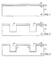
- FIG. 1 is a partial cross sectional view of a wafer at an intermediate stage in a fabrication process in which a hard mask is formed on a dielectric liner over a semiconductor substrate;
- FIG. 2 depicts processing subsequent to FIG. 1 in which trenches are formed in the semiconductor substrate
- FIG. 3 depicts processing subsequent to FIG. 2 in which the trenches are lined with a bottom dielectric
- FIG. 4 depicts processing subsequent to FIG. 3 in which source/drain regions are formed underlying the trenches
- FIG. 5 depicts processing subsequent to FIG. 4 in which a layer of discontinuous storage elements is deposited
- FIG. 6 depicts processing subsequent to FIG. 5 in which a top dielectric is formed on the layer of discontinuous storage elements
- FIG. 7 depicts processing subsequent to FIG. 6 in which a continuous control gate is formed resulting in a storage devices having hot carrier injection regions;
- FIG. 8 depicts a second embodiment of a storage device including a diffusion contact in the wafer surface
- FIG. 9 depicts a third embodiment of a storage device including a continuous control gate and staggered diffusion contacts
- FIG. 10 is a top view of an array based on the storage device of FIG. 7 ;
- FIG. 11 is a top view of an array based on the storage device of FIG. 8 ;
- FIG. 12 is a top view of an array based on the storage device of FIG. 9 ;
- FIG. 13 is a top view of an alternative layout to the device of FIG. 12 ;
- FIG. 14 is a programming table for the device of FIG. 7 ;
- FIG. 15 is a programming table for the device of FIG. 8 ;
- FIG. 16 is a programming table for the device of FIG. 9 ;
- FIG. 17 is an alternative embodiment of the array depicted in FIG. 8 .
- a semiconductor-based storage cell and a corresponding fabrication process employ a trench etched into a semiconductor substrate and a charge storage layer formed along the sidewalls of the trench.
- the charge storage layer preferably includes a set of discontinuous storage elements (DSEs).
- DSEs may be silicon nanocrystals, which are small, discreet silicon structures embedded in a dielectric layer and capable of holding a positive or negative charge. Because DSEs are not physically or electrically connected to each other, DSEs are less susceptible to charge loss through pin holes in the dielectric layer than conventional storage elements such as conventional polysilicon floating gate structures.
- the preferred implementation of the storage device is capable of storing multiple bits of information using hot carrier injection (HCI) programming, source side injection (SSI) programming, or both.
- HCI hot carrier injection
- SSI source side injection
- FIG. 1 through FIG. 7 depict a set of partial cross sectional views of a wafer at various stages in process for fabricating an embodiment of a nonvolatile storage device 100 .
- a dielectric liner 104 and a hard mask 106 are formed on an upper surface of a semiconductor substrate 102 of a semiconductor wafer 101 .
- Semiconductor substrate is preferably doped or undoped monocrystalline silicon.
- semiconductor substrate may include other semiconductors such as germanium or various semiconductor alloys such as the m-V semiconductor alloys including gallium arsenide.
- dielectric liner 104 is silicon oxide, which may be thermally formed (grown) or deposited using CVD (chemical vapor deposition).
- Hard mask 106 is preferably a dielectric that can be selectively etched with respect to substrate 102 .
- Hard mask 106 is preferably CVD silicon nitride, which is desirable for its ability to prevent oxidation of an underlying semiconductor.
- Hard mask 106 may include multiple dielectric layers.
- trenches 108 are formed in semiconductor substrate 102 .
- Trenches 108 define the structure of the storage device to be formed as will become evident in the following description. Formation of trenches 108 includes conventional photolithographic patterning of dielectric liner 104 and hard mask 106 followed by a dry etch process that etches the semiconductor material (e.g., silicon) preferentially with respect to liner 104 and hard mask 106 . Etch processes of this type are well known in the field of semiconductor fabrication. In the depicted implementation, trenches 108 have an aspect of approximately 1:2. A depth of trenches 108 is an implementation detail, but trenches having a depth in the range of approximately 50 nm to 300 nm are desirable for applications requiring dense storage arrays.
- bottom dielectric 110 is preferably a thin (e.g., 1 nm to 10 nm) high quality dielectric that is employed in the programming and erasing of the DSEs.
- a thin dielectric is preferred to achieve adequate programming times using either injection-based or tunneling-based programming techniques.
- a high quality dielectric is preferred to withstand the potentially large programming voltages and current and the potentially large number of programming cycles without exhibiting breakdown or significant leakage.
- bottom dielectric 110 is a thermally formed silicon dioxide film having a thickness in the range of approximately 4 to 10 nm. As depicted in FIG. 3 , where hard mask 106 is a silicon nitride hard mask, thermal oxidation of the trench walls does not substantially increase the thickness of dielectric liner 104 even for embodiments in which dielectric liner 104 is a silicon oxide.
- source/drain regions 112 are formed underlying trenches 108 .
- Source/drain regions 112 are electrically conductive, heavily-doped regions having a conductivity type opposite to a conductivity type of semiconductor substrate 102 .
- semiconductor substrate is preferably a lightly doped p-type (p ⁇ ) silicon and source/drain regions 112 are heavily doped n-doped (n+) silicon having an impurity distribution in excess of 1E18 cm ⁇ 3 .
- source/drain regions 112 are buried diffusion regions formed by implanting an impurity into substrate 102 underlying trenches 108 and thereafter performing a diffusion step. In other embodiments, the implantation step may be omitted to preserve the integrity of bottom oxide 110 .
- charge storage layer 121 represents the structure in or on which charge will be stored to program or erase the bit or bits of storage device 100 .
- charge storage layer 121 includes a plurality of DSEs 120 .
- DSEs 120 which are implemented as nanocrystals in some embodiments, are a set of discreet accumulations of a material capable of storing a charge. Suitable materials include silicon, polysilicon, metal materials including titanium, tantalum, aluminum, alloys thereof, and the like, and dielectrics such as silicon nitride or silicon oxynitride.
- DSEs 120 are silicon nanocrystals.
- DSEs 120 may be formed in any one of a variety of ways, preferably without requiring any photolithography steps.
- One well-known DSE formation technique is to deposit an amorphous silicon layer and heat it to form the nanocrystals.
- Another technique is to deposit the nanocrystals using chemical vapor deposition (CVD).
- DSEs may have various shapes, including hemispherical and spherical, depending upon the deposition technique employed.
- DSEs 120 are approximately 10 nm in diameter and are spaced at a predominantly uniform spacing of approximately 10 nm. Regardless of the formation technique used, each DSE 120 in this embodiment is a particle of silicon that is electrically and physically isolated from its neighbors.
- top dielectric 130 has been non-selectively formed overlying charge storage layer 121 to complete the formation of a charge storage stack, which includes bottom dielectric 110 , charge storage layer 121 , and top dielectric 130 .
- top dielectric 130 is a high temperature oxide (HTO) desirable for exhibiting characteristics (e.g., density and dielectric strength) substantially equivalent to thermally formed silicon dioxide.
- HTO high temperature oxide
- top dielectric 130 may be formed by a conventional HTO process such as by reacting dichlorosilane and nitrous oxide at temperatures approaching C.
- top dielectric 130 is preferably in the range of approximately 5 to 10 nm.
- control gate layer 140 is formed by non-selectively depositing an electrically conductive control gate material over wafer 101 including within trenches 108 ( FIG. 5 ). The deposited control gate material is then planarized (e.g., by chemical mechanical polish and/or etch back) to produce a substantially planar upper surface and patterned using conventional lithography and etch techniques.
- control gate layer 140 is formed by conventional CVD of polysilicon.
- the polysilicon may be doped either in situ or after deposition using ion implantation.
- control gate layer 140 may be doped with an n-type impurity such as arsenic or phosphorous.
- control gate layer 140 may include a metal such as aluminum, copper, titanium, tungsten, alloys thereof, or the like.
- Storage device 100 as depicted in FIG. 7 is a fully functional storage cell. More specifically, storage device 100 as depicted in FIG. 7 is a programmable storage device suitable for employing a hot carrier injection programming technique and capable of storing two bits of information (i.e., four unique states). As depicted in FIG. 7 , storage device 100 includes first and second source/drain regions 112 underlying first and second trenches 108 (see FIG. 6 ) defined in semiconductor substrate 102 . In one embodiment, source/drain regions 112 - 1 and 112 - 2 generically or collectively referred to as source/drain region(s) 112 ), extend parallel to one another in a plane perpendicular to the plane of cross section shown.
- Storage device 100 as depicted in FIG. 7 further includes a charge storage stack comprised of bottom oxide 104 , charge storage layer 121 , and top dielectric 130 .
- a control gate layer 140 of storage device 100 serves as the gate electrode for storage device 100 .
- control gate layer 140 is a continuous structure that fills the trenches 108 and traverses source/drain regions 112 - 1 and 112 - 2 . This embodiment is contrasted with an alternative implementation described below with respect to FIG. 8 .
- Storage device 100 is capable of storing two bits of information using HCI programming conditions.
- HCI programming localized regions of DSEs 120 , referred to as injection regions and indicated in FIG. 7 by reference numerals 114 - 1 and 114 - 2 , are programmed (have charge stored on them).
- Injection region 114 - 1 programmed using a first biasing condition, is associated with a first bit of storage device 100 while injection region 114 - 2 , programmed with a second biasing condition, is associated with a second bit of storage device 100 .
- Injection region 114 - 1 which includes DSEs 120 proximal to source/drain region 112 - 1 , is programmed by biasing control gate 140 to a gate programming voltage V PG , source/drain region 112 - 1 to a source/drain programming voltage V PD , and grounding source/drain region 112 - 2 and semiconductor substrate 102 .
- V PG and V PD are positive for NMOS structures (in which well 102 is p-doped and source/drain regions 112 are n-doped) with V PG preferably being larger than V PD in magnitude. In one embodiment, for example, V PG is preferably approximately 6 V while V PD is approximately 5 V.
- source/drain region 112 - 1 serves as the drain and electrons flow from source 112 - 2 to drain 112 - 1 along a conductive path formed in an upper portion of substrate 102 .
- electrons are accelerated by the electrical field resulting from the potential difference between drain 112 - 1 and source 112 - 2 , they are swept into a depletion region surrounding the biased drain.
- Some of these highly kinetic electrons collide with atoms in semiconductor substrate lattice and generate electron-hole pairs.
- Some of the electrons thus generated are injected into charge storage layer 121 by the electric field attributable to the positive bias on control gate layer 140 .
- This hot carrier injection process occurs primarily in a narrow injection zone, represented by reference numeral 114 - 1 in FIG. 7 , in proximity to drain 112 - 1 where the electrical field is at its maximum.
- the DSEs 120 encompassed by injection zone 114 - 1 retain injected charges and cause a detectable alteration in the electrical characteristics of the storage device. This alteration can be sensed during a read cycle as a change in I DS . As such, the charge stored on DSEs 120 in injection zone 114 - 1 correspond to a first bit of storage device 100 .
- a second injection zone 114 - 2 of charge storage device 100 including DSEs 120 proximal to source/drain region 112 - 2 , is programmed by switching the source/drain biases with source/drain 112 - 2 functioning as the biased drain terminal and source/drain region 112 - 1 serving as the grounded source terminal.
- Erasing injection zones 142 and 144 may be achieved by biasing control gate layer 140 to a negative potential (V E ) and biasing semiconductor substrate 102 to a positive value (V B ).
- V E negative potential
- V B biasing semiconductor substrate 102
- suitable values for V E and V B are ⁇ 6 V and 6 V respectively.
- the source/drain regions 112 may be floated during the erase operation. In this configuration, the erase operation erases both bits by simultaneously removing the stored charge from injection zones 114 - 1 and 114 - 2 .
- storage cell array 201 includes a set of parallel control gates 140 - 1 and 140 - 2 (generically or collectively referred to as control gate(s) 140 ), and a set of parallel source/drain regions 112 - 1 through 112 - n .
- Control gates 140 are oriented at right angles to source/drain regions 112 .
- the injection regions 114 - 1 and 114 - 2 of storage device 100 are shown as residing at edges of respective source/drain regions 112 - 1 and 112 - 2 where the DSEs 120 of FIG. 7 are positioned. (DSEs 120 are not themselves visible in the top view of FIG. 10 ).
- FIG. 11 An alternative embodiment of storage cell 200 is shown in the cross section of FIG. 8 and the top view of FIG. 11 .
- storage cell 200 includes a parallel pair of source drain regions 112 - 1 and 112 - 2 .
- the embodiment of storage cell 200 depicted in FIG. 8 and FIG. 11 employs a set of parallel control gates 140 - 1 , 140 - 2 , etc., which run parallel to trenches 112 .
- doping and isolation of the diffusion regions 152 may be achieved using a “striped” resist mask indicated by reference numeral 153 to form alternating n+ and p+ regions in substrate 102 .
- the implants (one n implant and one p implant) used to form these stripes are block by the control gates 140 as well as the resist masks.
- a variation of the embodiment depicted in FIG. 8 is the “virtual ground array” embodiment depicted in FIG. 17 .
- the diffusion region 152 of FIG. 8 is present, but without a contact within the array.
- the diffusion region 152 extends across the array parallel to source/drain regions 112 without making contact to a metalization layer within the array. Eliminating contact 152 simplifies the cell design and enables smaller cell sizes. Forming the diffusion region 152 without forming the contact may include using a masking step after forming the trenches to define the location of the isolation implants.
- contact structure 150 includes a conductive plug 151 within a void defined by sidewall spacers 154 .
- diffusion region 152 is of the same conductivity type as source/drain regions 112 (e.g., n-type for NMOS implementations).
- Storage cell 200 encompasses two storage devices 100 - 1 and 100 - 2 and a total of four bits indicated by HCI injection regions 114 - 1 through 114 - 4 .
- Storage device 100 - 1 of storage cell 200 includes control gate 140 - 1 , source/drain region 112 - 1 , and HCI programmable injection regions 114 - 1 and 114 - 3 while storage device 100 - 2 includes control gate 140 - 2 , source/drain region 112 - 2 , and injection regions 114 - 2 and 114 - 4 .
- Both storage cells use the contact 150 and the underlying source/drain region 152
- diffusion region 152 is vertically displaced relative to source/drain regions 112 .
- Charge storage layer 121 between source/drain region 112 and diffusion region 152 includes a vertical portion 122 overlying source/drain region 112 and a horizontal portion 124 adjacent diffusion region 152 .
- injection region 114 - 3 of storage device 100 - 1 encompasses the DSEs 120 in the horizontal portion 124 of charge storage layer 121 proximal to diffusion region 152 .
- injection region 114 - 4 of storage device 100 - 2 encompasses the DSEs 120 in horizontal portion 122 of charge storage layer 121 proximal to an opposing side of diffusion region 152 .
- Programming injection region 114 - 3 of storage device 100 - 1 includes biasing diffusion region 152 to V PD , control gate 140 - 1 to V PG , and source drain region 112 - 1 and semiconductor substrate to ground.
- Programming injection region 114 - 4 includes biasing diffusion region 152 to V PD , control gate 140 - 2 to V PG , and source/drain region 112 - 2 and semiconductor substrate to ground.
- Storage cell 200 is shown in FIG. 12 without backend metallization. In one embodiment, this metalization would includes diffusion region metalization connecting to contacts 150 - 1 and 150 - 2 .
- each storage cell 200 in array 201 includes a continuous control gate layer 140 and a pair of “staggered” contacts 150 - 1 and 150 - 2 .
- Contacts 150 - 1 and 150 - 2 are displaced with respect to control gate layer 140 such that first contact 150 - 1 is positioned on a first side of control gate layer 140 while second contact 150 - 2 is positioned on a second side of control gate layer 140 .
- This embodiment produces a storage cell 200 that includes four devices 100 - 1 through 100 - 4 and four HCI programmable bits corresponding to injection regions 114 - 1 through 114 - 4 .
- Injection regions 114 - 1 through 114 - 4 include a pair of injection regions 114 - 1 and 114 - 2 located in the DSEs at the edge of source/drain region 112 - 1 and a pair of injection regions 114 - 3 and 114 - 4 located in the DSEs at the edge of source/drain region 112 - 2 .
- Injection region 114 - 1 is associated with storage device 100 - 1
- injection region 114 - 2 is associated with storage device 100 - 2
- Storage device 100 - 1 includes control gate 140 , source/drain region 112 - 1 , and the diffusion region 152 - 1 underlying contact 150 - 1 .
- Storage device 100 - 2 includes control gate 140 , source/drain region 112 - 1 , and the diffusion region 152 - 2 underlying contact 150 - 2 .
- injection regions 114 - 1 and 114 - 2 are located in a common sidewall of charge storage layer 121 . As seen in FIG. 12 and FIG. 13 , injection region 114 - 1 is closer to contact 150 - 1 while injection region 114 - 2 is close to contact 150 - 2 .
- contacts 150 - 1 are 150 - 2 are staggered such that first contact 150 - 1 is closer to source/drain region 112 - 1 while second contact 150 - 2 is closer to source/drain region 112 - 2 .
- contacts 150 - 1 and 150 - 2 as depicted in FIG. 13 lie along a line that is parallel to the orientation of source/drain regions 112 - 1 and 112 - 2 such that the contacts are equidistant from source/drain regions 112 - 1 .
- contacts 150 - 1 and 150 - 2 are intended to be electrically distinct such that a first metal interconnect (not depicted) contacts first contact 150 - 1 while a second metal line contacts contact 150 - 2 .
- the arrangement of contacts 150 as depicted in FIG. 12 simplifies the design of the metallization, but introduces an asymmetry in the configuration of the resulting transistors.
- An injection region 114 - 1 of storage device 100 - 1 is programmed by biasing source/drain region 112 - 1 to V PD , control gate 140 to V PG , grounding semiconductor substrate 102 and diffusion region 152 - 1 underlying contact 150 - 1 , and floating source/drain region 152 - 2 .
- programming second injection region 114 - 2 includes biasing source/drain region 112 - 1 to V PD , control gate layer 140 to V PG , grounding diffusion region 152 - 2 and semiconductor substrate 102 , and floating source/drain contact 150 - 1 .
- Analogous biasing is used to program injection regions 114 - 3 and 114 - 4 of electrical devices 100 - 3 and 100 - 4 respectively with the biasing of source/drain region 112 - 2 substituting for the biasing of source/drain regions 112 - 1 .
- Programming tables 145 , 146 , and 147 depicted in FIG. 14 , FIG. 15 , and FIG. 16 respectively summarize the bias conditions for program and erase operations with respect to storage cell 100 as depicted in FIG. 7 , FIG. 8 , and FIG. 9 respectively.
- programming an injection region 114 is achieved by biasing the appropriate control gate to V PG and one of the device's source/drain electrodes to V PD .
- the other source/drain electrode and the substrate also referred to as the well) are grounded.
- the source/drain electrodes for device 100 are the source/drain regions 112 - 1 and 112 - 1 .
- the source/drain electrodes of the storage device include one of the source/drain regions 112 and the diffusion region 152 .
- the source/drain electrodes include one of the source/drain regions 112 and one of the diffusion regions 152 .
- V PG may be in the range of approximately 6 to 9 V
- V PD in the range of approximately 3 to 6 V
- V EG in the range of approximately ⁇ 6 to ⁇ 9 V.
- a read operation may use a biasing configuration analogous to the programming biasing configuration, but having lower voltage magnitudes. It will be appreciated by those skilled in the design of electrically programmable storage cells that circuits capable of producing the required programming, erase, and read biasing conditions are well known.
Abstract
Description
Claims (20)
Priority Applications (1)
| Application Number | Priority Date | Filing Date | Title |
|---|---|---|---|
| US11/188,583 US7314798B2 (en) | 2005-07-25 | 2005-07-25 | Method of fabricating a nonvolatile storage array with continuous control gate employing hot carrier injection programming |
Applications Claiming Priority (1)
| Application Number | Priority Date | Filing Date | Title |
|---|---|---|---|
| US11/188,583 US7314798B2 (en) | 2005-07-25 | 2005-07-25 | Method of fabricating a nonvolatile storage array with continuous control gate employing hot carrier injection programming |
Publications (2)
| Publication Number | Publication Date |
|---|---|
| US20070020831A1 US20070020831A1 (en) | 2007-01-25 |
| US7314798B2 true US7314798B2 (en) | 2008-01-01 |
Family
ID=37679589
Family Applications (1)
| Application Number | Title | Priority Date | Filing Date |
|---|---|---|---|
| US11/188,583 Expired - Fee Related US7314798B2 (en) | 2005-07-25 | 2005-07-25 | Method of fabricating a nonvolatile storage array with continuous control gate employing hot carrier injection programming |
Country Status (1)
| Country | Link |
|---|---|
| US (1) | US7314798B2 (en) |
Cited By (5)
| Publication number | Priority date | Publication date | Assignee | Title |
|---|---|---|---|---|
| US20070018221A1 (en) * | 2005-07-25 | 2007-01-25 | Freescale Semiconductor, Inc. | Programmable structure including discontinuous storage elements and spacer control gates in a trench |
| US7692972B1 (en) | 2008-07-22 | 2010-04-06 | Actel Corporation | Split gate memory cell for programmable circuit device |
| US20110063923A1 (en) * | 2006-12-04 | 2011-03-17 | Micron Technology, Inc. | Trench memory structure operation |
| US20110220986A1 (en) * | 2010-03-15 | 2011-09-15 | Macronix International Co., Ltd. | Memory device and method for fabricating the same |
| US8193572B2 (en) | 2007-01-24 | 2012-06-05 | Freescale Semiconductor, Inc. | Electronic device including trenches and discontinuous storage elements |
Families Citing this family (6)
| Publication number | Priority date | Publication date | Assignee | Title |
|---|---|---|---|---|
| US7262997B2 (en) * | 2005-07-25 | 2007-08-28 | Freescale Semiconductor, Inc. | Process for operating an electronic device including a memory array and conductive lines |
| US8320191B2 (en) | 2007-08-30 | 2012-11-27 | Infineon Technologies Ag | Memory cell arrangement, method for controlling a memory cell, memory array and electronic device |
| US8951892B2 (en) | 2012-06-29 | 2015-02-10 | Freescale Semiconductor, Inc. | Applications for nanopillar structures |
| US8853027B2 (en) | 2012-10-01 | 2014-10-07 | Freescale Semiconductor, Inc. | Split gate flash cell |
| WO2014070163A1 (en) | 2012-10-31 | 2014-05-08 | Hewlett-Packard Development Company, L.P. | Memory cell that prevents charge loss |
| CN108630521B (en) * | 2017-03-17 | 2020-11-03 | 中芯国际集成电路制造(上海)有限公司 | Method for manufacturing semiconductor device |
Citations (59)
| Publication number | Priority date | Publication date | Assignee | Title |
|---|---|---|---|---|
| US4184207A (en) * | 1978-01-27 | 1980-01-15 | Texas Instruments Incorporated | High density floating gate electrically programmable ROM |
| US4751558A (en) * | 1985-10-31 | 1988-06-14 | International Business Machines Corporation | High density memory with field shield |
| US4785337A (en) * | 1986-10-17 | 1988-11-15 | International Business Machines Corporation | Dynamic ram cell having shared trench storage capacitor with sidewall-defined bridge contacts and gate electrodes |
| US4833094A (en) * | 1986-10-17 | 1989-05-23 | International Business Machines Corporation | Method of making a dynamic ram cell having shared trench storage capacitor with sidewall-defined bridge contacts and gate electrodes |
| US4860070A (en) * | 1987-01-09 | 1989-08-22 | Mitsubishi Denki Kabushiki Kaisha | Semiconductor memory device comprising trench memory cells |
| US5196722A (en) | 1992-03-12 | 1993-03-23 | International Business Machines Corporation | Shadow ram cell having a shallow trench eeprom |
| US5252845A (en) | 1990-04-02 | 1993-10-12 | Electronics And Telecommunications Research Institute | Trench DRAM cell with vertical transistor |
| US5315142A (en) * | 1992-03-23 | 1994-05-24 | International Business Machines Corporation | High performance trench EEPROM cell |
| US5432365A (en) * | 1988-02-15 | 1995-07-11 | Samsung Electronics Co., Ltd. | Semiconductor memory device |
| US5705415A (en) | 1994-10-04 | 1998-01-06 | Motorola, Inc. | Process for forming an electrically programmable read-only memory cell |
| US5721448A (en) * | 1996-07-30 | 1998-02-24 | International Business Machines Corporation | Integrated circuit chip having isolation trenches composed of a dielectric layer with oxidation catalyst material |
| US5824580A (en) * | 1996-07-30 | 1998-10-20 | International Business Machines Corporation | Method of manufacturing an insulated gate field effect transistor |
| US5914523A (en) * | 1998-02-17 | 1999-06-22 | National Semiconductor Corp. | Semiconductor device trench isolation structure with polysilicon bias voltage contact |
| US5923046A (en) | 1996-09-13 | 1999-07-13 | Kabushiki Kaisha Toshiba | Quantum dot memory cell |
| US5969383A (en) | 1997-06-16 | 1999-10-19 | Motorola, Inc. | Split-gate memory device and method for accessing the same |
| US5998263A (en) * | 1996-05-16 | 1999-12-07 | Altera Corporation | High-density nonvolatile memory cell |
| US6074954A (en) * | 1998-08-31 | 2000-06-13 | Applied Materials, Inc | Process for control of the shape of the etch front in the etching of polysilicon |
| US6117733A (en) | 1998-05-27 | 2000-09-12 | Taiwan Semiconductor Manufacturing Company | Poly tip formation and self-align source process for split-gate flash cell |
| US6228706B1 (en) | 1999-08-26 | 2001-05-08 | International Business Machines Corporation | Vertical DRAM cell with TFT over trench capacitor |
| US6265268B1 (en) | 1999-10-25 | 2001-07-24 | Advanced Micro Devices, Inc. | High temperature oxide deposition process for fabricating an ONO floating-gate electrode in a two bit EEPROM device |
| US6281064B1 (en) | 1999-06-04 | 2001-08-28 | International Business Machines Corporation | Method for providing dual work function doping and protective insulating cap |
| US6307782B1 (en) | 2000-04-03 | 2001-10-23 | Motorola, Inc. | Process for operating a semiconductor device |
| US6320784B1 (en) | 2000-03-14 | 2001-11-20 | Motorola, Inc. | Memory cell and method for programming thereof |
| US6330184B1 (en) | 2000-02-01 | 2001-12-11 | Motorola, Inc. | Method of operating a semiconductor device |
| US6365452B1 (en) | 1998-03-19 | 2002-04-02 | Lsi Logic Corporation | DRAM cell having a vertical transistor and a capacitor formed on the sidewalls of a trench isolation |
| US6399441B1 (en) | 1999-08-05 | 2002-06-04 | Halo Lsi Device & Design Technology, Inc. | Nonvolatile memory cell, method of programming the same and nonvolatile memory array |
| US20020151136A1 (en) | 1998-03-05 | 2002-10-17 | Taiwan Semiconductor Manufacturing Company | Method of manufacture of vertical split gate flash memory device and device manufactured thereby |
| US6486028B1 (en) * | 2001-11-20 | 2002-11-26 | Macronix International Co., Ltd. | Method of fabricating a nitride read-only-memory cell vertical structure |
| US20030062565A1 (en) | 1996-01-22 | 2003-04-03 | Semiconductor Energy Laboratory Co., Ltd., A Japanese Corporation | Semiconductor device and method of fabricating same |
| US20030068864A1 (en) | 2001-10-10 | 2003-04-10 | Park Il-Yong | Method for fabricating power semiconductor device having trench gate structure |
| US6559032B2 (en) | 1996-01-05 | 2003-05-06 | Micron Technology, Inc. | Method of fabricating an isolation structure on a semiconductor substrate |
| US6638810B2 (en) | 2000-02-22 | 2003-10-28 | Applied Materials, Inc. | Tantalum nitride CVD deposition by tantalum oxide densification |
| US20040000688A1 (en) * | 2001-05-18 | 2004-01-01 | Sandisk Corporation | Non-volatile memory cells utilizing substrate trenches |
| US6674120B2 (en) | 2000-05-02 | 2004-01-06 | Sony Corporation | Nonvolatile semiconductor memory device and method of operation thereof |
| US6673681B2 (en) | 1999-05-19 | 2004-01-06 | Fairchild Semiconductor Corporation | Process for forming MOS-gated power device having segmented trench and extended doping zone |
| US6677204B2 (en) | 2000-08-14 | 2004-01-13 | Matrix Semiconductor, Inc. | Multigate semiconductor device with vertical channel current and method of fabrication |
| US6706599B1 (en) | 2003-03-20 | 2004-03-16 | Motorola, Inc. | Multi-bit non-volatile memory device and method therefor |
| US6750499B2 (en) | 2002-08-06 | 2004-06-15 | Intelligent Sources Development Corp. | Self-aligned trench-type dram structure and its contactless dram arrays |
| US20040121540A1 (en) | 2002-12-17 | 2004-06-24 | Chi-Hui Lin | Stacked gate flash memory device and method of fabricating the same |
| US6803620B2 (en) | 2000-10-27 | 2004-10-12 | Sony Corporation | Non-volatile semiconductor memory device and a method of producing the same |
| US6818512B1 (en) | 2002-01-04 | 2004-11-16 | Taiwan Semiconductor Manufacturing Company | Split-gate flash with source/drain multi-sharing |
| US6818939B1 (en) | 2003-07-18 | 2004-11-16 | Semiconductor Components Industries, L.L.C. | Vertical compound semiconductor field effect transistor structure |
| US20040248371A1 (en) | 2003-06-06 | 2004-12-09 | Chih-Hsin Wang | Floating-gate memory cell having trench structure with ballastic-charge injector and array of memory cells |
| US20050037576A1 (en) * | 2003-08-14 | 2005-02-17 | Bomy Chen | Method of manufacturing an array of bi-directional nonvolatile memory cells |
| US6894339B2 (en) | 2003-01-02 | 2005-05-17 | Actrans System Inc. | Flash memory with trench select gate and fabrication process |
| US20050148173A1 (en) | 2004-01-05 | 2005-07-07 | Fuja Shone | Non-volatile memory array having vertical transistors and manufacturing method thereof |
| US6916715B2 (en) | 2002-11-18 | 2005-07-12 | Nanya Technology Corporation | Method for fabricating a vertical NROM cell |
| US20050259475A1 (en) * | 2004-05-18 | 2005-11-24 | Micron Technology, Inc. | Ballistic injection nrom flash memory |
| US20050280089A1 (en) * | 2003-11-17 | 2005-12-22 | Micron Technology, Inc. | NROM flash memory devices on ultrathin silicon |
| US20060011966A1 (en) | 2004-07-15 | 2006-01-19 | Promos Technologies Inc. | Structure of a non-volatile memory cell and method of forming the same |
| US20060046383A1 (en) | 2004-09-02 | 2006-03-02 | Shenlin Chen | Method for forming a nanocrystal floating gate for a flash memory device |
| US7015537B2 (en) | 2004-04-12 | 2006-03-21 | Silicon Storage Technology, Inc. | Isolation-less, contact-less array of nonvolatile memory cells each having a floating gate for storage of charges, and methods of manufacturing, and operating therefor |
| US20060131640A1 (en) | 2004-03-16 | 2006-06-22 | Andy Yu | Memory array of non-volatile electrically alterable memory cells for storing multiple data |
| US20060152978A1 (en) * | 2003-12-16 | 2006-07-13 | Micron Technology, Inc. | Multi-state NROM device |
| US7078286B1 (en) | 2002-09-06 | 2006-07-18 | Lattice Semiconductor Corporation | Process for fabricating a semiconductor device having electrically isolated low voltage and high voltage regions |
| US7098502B2 (en) | 2003-11-10 | 2006-08-29 | Freescale Semiconductor, Inc. | Transistor having three electrically isolated electrodes and method of formation |
| US7199419B2 (en) | 2004-12-13 | 2007-04-03 | Micron Technology, Inc. | Memory structure for reduced floating body effect |
| US7211858B2 (en) * | 2005-07-25 | 2007-05-01 | Freescale Semiconductor, Inc. | Split gate storage device including a horizontal first gate and a vertical second gate in a trench |
| US7220634B2 (en) | 2002-06-21 | 2007-05-22 | Micron Technology, Inc. | NROM memory cell, memory array, related devices and methods |
Family Cites Families (1)
| Publication number | Priority date | Publication date | Assignee | Title |
|---|---|---|---|---|
| US6537870B1 (en) * | 2000-09-29 | 2003-03-25 | Infineon Technologies Ag | Method of forming an integrated circuit comprising a self aligned trench |
-
2005
- 2005-07-25 US US11/188,583 patent/US7314798B2/en not_active Expired - Fee Related
Patent Citations (65)
| Publication number | Priority date | Publication date | Assignee | Title |
|---|---|---|---|---|
| US4184207A (en) * | 1978-01-27 | 1980-01-15 | Texas Instruments Incorporated | High density floating gate electrically programmable ROM |
| US4751558A (en) * | 1985-10-31 | 1988-06-14 | International Business Machines Corporation | High density memory with field shield |
| US4785337A (en) * | 1986-10-17 | 1988-11-15 | International Business Machines Corporation | Dynamic ram cell having shared trench storage capacitor with sidewall-defined bridge contacts and gate electrodes |
| US4833094A (en) * | 1986-10-17 | 1989-05-23 | International Business Machines Corporation | Method of making a dynamic ram cell having shared trench storage capacitor with sidewall-defined bridge contacts and gate electrodes |
| US4860070A (en) * | 1987-01-09 | 1989-08-22 | Mitsubishi Denki Kabushiki Kaisha | Semiconductor memory device comprising trench memory cells |
| US5432365A (en) * | 1988-02-15 | 1995-07-11 | Samsung Electronics Co., Ltd. | Semiconductor memory device |
| US5252845A (en) | 1990-04-02 | 1993-10-12 | Electronics And Telecommunications Research Institute | Trench DRAM cell with vertical transistor |
| US5196722A (en) | 1992-03-12 | 1993-03-23 | International Business Machines Corporation | Shadow ram cell having a shallow trench eeprom |
| US5315142A (en) * | 1992-03-23 | 1994-05-24 | International Business Machines Corporation | High performance trench EEPROM cell |
| US5567635A (en) * | 1992-03-23 | 1996-10-22 | International Business Machines Corporation | Method of making a three dimensional trench EEPROM cell structure |
| US5705415A (en) | 1994-10-04 | 1998-01-06 | Motorola, Inc. | Process for forming an electrically programmable read-only memory cell |
| US6559032B2 (en) | 1996-01-05 | 2003-05-06 | Micron Technology, Inc. | Method of fabricating an isolation structure on a semiconductor substrate |
| US20030062565A1 (en) | 1996-01-22 | 2003-04-03 | Semiconductor Energy Laboratory Co., Ltd., A Japanese Corporation | Semiconductor device and method of fabricating same |
| US5998263A (en) * | 1996-05-16 | 1999-12-07 | Altera Corporation | High-density nonvolatile memory cell |
| US5721448A (en) * | 1996-07-30 | 1998-02-24 | International Business Machines Corporation | Integrated circuit chip having isolation trenches composed of a dielectric layer with oxidation catalyst material |
| US5824580A (en) * | 1996-07-30 | 1998-10-20 | International Business Machines Corporation | Method of manufacturing an insulated gate field effect transistor |
| US5923046A (en) | 1996-09-13 | 1999-07-13 | Kabushiki Kaisha Toshiba | Quantum dot memory cell |
| US5969383A (en) | 1997-06-16 | 1999-10-19 | Motorola, Inc. | Split-gate memory device and method for accessing the same |
| US5914523A (en) * | 1998-02-17 | 1999-06-22 | National Semiconductor Corp. | Semiconductor device trench isolation structure with polysilicon bias voltage contact |
| US6121148A (en) * | 1998-02-17 | 2000-09-19 | National Semiconductor Corporation | Semiconductor device trench isolation structure with polysilicon bias voltage contact |
| US6583466B2 (en) * | 1998-03-05 | 2003-06-24 | Taiwan Semiconductor Manufacturing Company | Vertical split gate flash memory device in an orthogonal array of rows and columns with devices in columns having shared source regions |
| US20020151136A1 (en) | 1998-03-05 | 2002-10-17 | Taiwan Semiconductor Manufacturing Company | Method of manufacture of vertical split gate flash memory device and device manufactured thereby |
| US6365452B1 (en) | 1998-03-19 | 2002-04-02 | Lsi Logic Corporation | DRAM cell having a vertical transistor and a capacitor formed on the sidewalls of a trench isolation |
| US6117733A (en) | 1998-05-27 | 2000-09-12 | Taiwan Semiconductor Manufacturing Company | Poly tip formation and self-align source process for split-gate flash cell |
| US6074954A (en) * | 1998-08-31 | 2000-06-13 | Applied Materials, Inc | Process for control of the shape of the etch front in the etching of polysilicon |
| US6673681B2 (en) | 1999-05-19 | 2004-01-06 | Fairchild Semiconductor Corporation | Process for forming MOS-gated power device having segmented trench and extended doping zone |
| US6281064B1 (en) | 1999-06-04 | 2001-08-28 | International Business Machines Corporation | Method for providing dual work function doping and protective insulating cap |
| US6399441B1 (en) | 1999-08-05 | 2002-06-04 | Halo Lsi Device & Design Technology, Inc. | Nonvolatile memory cell, method of programming the same and nonvolatile memory array |
| US6228706B1 (en) | 1999-08-26 | 2001-05-08 | International Business Machines Corporation | Vertical DRAM cell with TFT over trench capacitor |
| US6265268B1 (en) | 1999-10-25 | 2001-07-24 | Advanced Micro Devices, Inc. | High temperature oxide deposition process for fabricating an ONO floating-gate electrode in a two bit EEPROM device |
| US6330184B1 (en) | 2000-02-01 | 2001-12-11 | Motorola, Inc. | Method of operating a semiconductor device |
| US6638810B2 (en) | 2000-02-22 | 2003-10-28 | Applied Materials, Inc. | Tantalum nitride CVD deposition by tantalum oxide densification |
| US6320784B1 (en) | 2000-03-14 | 2001-11-20 | Motorola, Inc. | Memory cell and method for programming thereof |
| US6307782B1 (en) | 2000-04-03 | 2001-10-23 | Motorola, Inc. | Process for operating a semiconductor device |
| US6674120B2 (en) | 2000-05-02 | 2004-01-06 | Sony Corporation | Nonvolatile semiconductor memory device and method of operation thereof |
| US6677204B2 (en) | 2000-08-14 | 2004-01-13 | Matrix Semiconductor, Inc. | Multigate semiconductor device with vertical channel current and method of fabrication |
| US6803620B2 (en) | 2000-10-27 | 2004-10-12 | Sony Corporation | Non-volatile semiconductor memory device and a method of producing the same |
| US20040000688A1 (en) * | 2001-05-18 | 2004-01-01 | Sandisk Corporation | Non-volatile memory cells utilizing substrate trenches |
| US6936887B2 (en) | 2001-05-18 | 2005-08-30 | Sandisk Corporation | Non-volatile memory cells utilizing substrate trenches |
| US20030068864A1 (en) | 2001-10-10 | 2003-04-10 | Park Il-Yong | Method for fabricating power semiconductor device having trench gate structure |
| US6486028B1 (en) * | 2001-11-20 | 2002-11-26 | Macronix International Co., Ltd. | Method of fabricating a nitride read-only-memory cell vertical structure |
| US6818512B1 (en) | 2002-01-04 | 2004-11-16 | Taiwan Semiconductor Manufacturing Company | Split-gate flash with source/drain multi-sharing |
| US7220634B2 (en) | 2002-06-21 | 2007-05-22 | Micron Technology, Inc. | NROM memory cell, memory array, related devices and methods |
| US6750499B2 (en) | 2002-08-06 | 2004-06-15 | Intelligent Sources Development Corp. | Self-aligned trench-type dram structure and its contactless dram arrays |
| US7078286B1 (en) | 2002-09-06 | 2006-07-18 | Lattice Semiconductor Corporation | Process for fabricating a semiconductor device having electrically isolated low voltage and high voltage regions |
| US6916715B2 (en) | 2002-11-18 | 2005-07-12 | Nanya Technology Corporation | Method for fabricating a vertical NROM cell |
| US20040121540A1 (en) | 2002-12-17 | 2004-06-24 | Chi-Hui Lin | Stacked gate flash memory device and method of fabricating the same |
| US6894339B2 (en) | 2003-01-02 | 2005-05-17 | Actrans System Inc. | Flash memory with trench select gate and fabrication process |
| US6706599B1 (en) | 2003-03-20 | 2004-03-16 | Motorola, Inc. | Multi-bit non-volatile memory device and method therefor |
| US20040248371A1 (en) | 2003-06-06 | 2004-12-09 | Chih-Hsin Wang | Floating-gate memory cell having trench structure with ballastic-charge injector and array of memory cells |
| US6818939B1 (en) | 2003-07-18 | 2004-11-16 | Semiconductor Components Industries, L.L.C. | Vertical compound semiconductor field effect transistor structure |
| US20050037576A1 (en) * | 2003-08-14 | 2005-02-17 | Bomy Chen | Method of manufacturing an array of bi-directional nonvolatile memory cells |
| US7098502B2 (en) | 2003-11-10 | 2006-08-29 | Freescale Semiconductor, Inc. | Transistor having three electrically isolated electrodes and method of formation |
| US20050280089A1 (en) * | 2003-11-17 | 2005-12-22 | Micron Technology, Inc. | NROM flash memory devices on ultrathin silicon |
| US20050280094A1 (en) * | 2003-11-17 | 2005-12-22 | Micron Technology, Inc. | NROM flash memory devices on ultrathin silicon |
| US20060152978A1 (en) * | 2003-12-16 | 2006-07-13 | Micron Technology, Inc. | Multi-state NROM device |
| US20060166443A1 (en) * | 2003-12-16 | 2006-07-27 | Micron Technology, Inc. | Multi-state NROM device |
| US20050148173A1 (en) | 2004-01-05 | 2005-07-07 | Fuja Shone | Non-volatile memory array having vertical transistors and manufacturing method thereof |
| US20060131640A1 (en) | 2004-03-16 | 2006-06-22 | Andy Yu | Memory array of non-volatile electrically alterable memory cells for storing multiple data |
| US7015537B2 (en) | 2004-04-12 | 2006-03-21 | Silicon Storage Technology, Inc. | Isolation-less, contact-less array of nonvolatile memory cells each having a floating gate for storage of charges, and methods of manufacturing, and operating therefor |
| US20050259475A1 (en) * | 2004-05-18 | 2005-11-24 | Micron Technology, Inc. | Ballistic injection nrom flash memory |
| US20060011966A1 (en) | 2004-07-15 | 2006-01-19 | Promos Technologies Inc. | Structure of a non-volatile memory cell and method of forming the same |
| US20060046383A1 (en) | 2004-09-02 | 2006-03-02 | Shenlin Chen | Method for forming a nanocrystal floating gate for a flash memory device |
| US7199419B2 (en) | 2004-12-13 | 2007-04-03 | Micron Technology, Inc. | Memory structure for reduced floating body effect |
| US7211858B2 (en) * | 2005-07-25 | 2007-05-01 | Freescale Semiconductor, Inc. | Split gate storage device including a horizontal first gate and a vertical second gate in a trench |
Non-Patent Citations (29)
| Title |
|---|
| "Twin MONOS Cell with Dual Control Gates," VLSI Technology, Source-Side Injection Cell with Two Storage Regions Forming in Nitride, p. 122, 2000. |
| "Vertical Floating-Gate 4.5/sup 2/split-gate NOR Flash Memory at 110nm Node," VLSI Technology, Source-Side Injection Cell in a Trench, p. 72, 2004. |
| Actions on the Merits by U.S.P.T.O, as of Jul. 26, 2007, 8 pages. |
| Guan, H., et al. "An Analytical Model for Optimization of Programming Efficiency and Uniformity of Split Gate Source-Side Injection Superflash Memory," IEEE Transactions on Electron Devices, vol. 50, No. 3, pp. 809-815, Mar. 2003. |
| Hayashi, Y., et al. "Twin MONOS Cell with Dual Control Gates," 2000 Symposium on VLSI Technology Digest of Technical Papers, pp. 122-123, 2000. |
| Lee, D., et al. "Vertical Floating-Gate 4.5F2 Split-Gate NOR Flash Memory at 110nm Node," 2004 Symposium on VLSI Technology Digest of Technical Papers, pp. 72-73, 2004. |
| Ma, et al. "A Dual-Bit Split-Gate EEPROM (DSG) Cell in Contactless Array for Single-Vcc High Density Flash Memories," IEDM, p. 57-60, 1994. |
| Osabe, et al. "Charge-Injection Length in Silicon Nanocrystal Memory Cells," VLSI, p. 242, 2004. |
| U.S. Appl. No. 10/961,295, filed Oct. 8, 2004. |
| U.S. Appl. No. 11/188,582, filed Jul. 25, 2005. |
| U.S. Appl. No. 11/188,584, filed Jul. 25, 2005. |
| U.S. Appl. No. 11/188,585, filed Jul. 25, 2005. |
| U.S. Appl. No. 11/188,588, filed Jul. 25, 2005. |
| U.S. Appl. No. 11/188,591, filed Jul. 25, 2005. |
| U.S. Appl. No. 11/188,603, filed Jul. 25, 2005. |
| U.S. Appl. No. 11/188,604, filed Jul. 25, 2005. |
| U.S. Appl. No. 11/188,615, filed Jul. 25, 2005. |
| U.S. Appl. No. 11/188,898, filed Jul. 25, 2005. |
| U.S. Appl. No. 11/188,909, filed Jul. 25, 2005. |
| U.S. Appl. No. 11/188,910, filed Jul. 25, 2005. |
| U.S. Appl. No. 11/188,935, filed Jul. 25, 2005. |
| U.S. Appl. No. 11/188,939, filed Jul. 25, 2005. |
| U.S. Appl. No. 11/188,953, filed Jul. 25, 2005. |
| U.S. Appl. No. 11/188,999, filed Jul. 25, 2005. |
| U.S. Appl. No. 11/525,747, filed Sep. 22, 2006. |
| U.S. Appl. No. 11/626,753, filed Jan. 24, 2007. |
| U.S. Appl. No. 11/626,762, filed Jan. 24, 2007. |
| U.S. Appl. No. 11/626,768, filed Jan. 24, 2007. |
| Van Houdt, J., et al. "An Analytical Model for the Optimization of Source-Side Injection Flash EEPROM Devices," IEEE Transactions on Electron Devices, vol. 42, No. 7, pp. 1314-1320, Jul. 1995. |
Cited By (8)
| Publication number | Priority date | Publication date | Assignee | Title |
|---|---|---|---|---|
| US20070018221A1 (en) * | 2005-07-25 | 2007-01-25 | Freescale Semiconductor, Inc. | Programmable structure including discontinuous storage elements and spacer control gates in a trench |
| US7394686B2 (en) * | 2005-07-25 | 2008-07-01 | Freescale Semiconductor, Inc. | Programmable structure including discontinuous storage elements and spacer control gates in a trench |
| US20110063923A1 (en) * | 2006-12-04 | 2011-03-17 | Micron Technology, Inc. | Trench memory structure operation |
| US8284616B2 (en) * | 2006-12-04 | 2012-10-09 | Micron Technology, Inc. | Trench memory structure operation |
| US8193572B2 (en) | 2007-01-24 | 2012-06-05 | Freescale Semiconductor, Inc. | Electronic device including trenches and discontinuous storage elements |
| US7692972B1 (en) | 2008-07-22 | 2010-04-06 | Actel Corporation | Split gate memory cell for programmable circuit device |
| US20110220986A1 (en) * | 2010-03-15 | 2011-09-15 | Macronix International Co., Ltd. | Memory device and method for fabricating the same |
| US8836004B2 (en) * | 2010-03-15 | 2014-09-16 | Macronix International Co., Ltd. | Memory device |
Also Published As
| Publication number | Publication date |
|---|---|
| US20070020831A1 (en) | 2007-01-25 |
Similar Documents
| Publication | Publication Date | Title |
|---|---|---|
| US7285819B2 (en) | Nonvolatile storage array with continuous control gate employing hot carrier injection programming | |
| US7314798B2 (en) | Method of fabricating a nonvolatile storage array with continuous control gate employing hot carrier injection programming | |
| US7459744B2 (en) | Hot carrier injection programmable structure including discontinuous storage elements and spacer control gates in a trench and a method of using the same | |
| US7592224B2 (en) | Method of fabricating a storage device including decontinuous storage elements within and between trenches | |
| US10950608B2 (en) | Semiconductor device having junctionless vertical gate transistor and method of manufacturing the same | |
| US10741698B2 (en) | Semi-floating gate FET | |
| US7250340B2 (en) | Method of fabricating programmable structure including discontinuous storage elements and spacer control gates in a trench | |
| US20070020840A1 (en) | Programmable structure including nanocrystal storage elements in a trench | |
| US7211858B2 (en) | Split gate storage device including a horizontal first gate and a vertical second gate in a trench | |
| KR100587782B1 (en) | Bottle-shaped trench capacitor with epi buried layer | |
| KR101923791B1 (en) | Non-volatile memory cell with self aligned floating and erase gates, and method of making same | |
| US9748332B1 (en) | Non-volatile semiconductor memory | |
| JP2007511090A (en) | Transistor having three electrically insulated electrodes and method of forming the transistor | |
| EP2147461A1 (en) | Nonvolatile memory cell comprising a nanowire and manufacturing method thereof | |
| US7394686B2 (en) | Programmable structure including discontinuous storage elements and spacer control gates in a trench | |
| US8587036B2 (en) | Non-volatile memory and fabricating method thereof | |
| US20070128799A1 (en) | Method of fabricating flash memory | |
| US8344446B2 (en) | Nonvolatile storage device and method for manufacturing the same in which insulating film is located between first and second impurity diffusion regions but absent on first impurity diffusion region | |
| US8815680B2 (en) | Non-volatile memory having nano crystalline silicon hillocks floating gate | |
| US7602005B2 (en) | Memory devices including spacer-shaped electrodes on pedestals and methods of manufacturing the same | |
| US8471323B2 (en) | 3-D electrically programmable and erasable single-transistor non-volatile semiconductor memory device | |
| US20230083560A1 (en) | Field effect transistors with gate fins and method of making the same |
Legal Events
| Date | Code | Title | Description |
|---|---|---|---|
| AS | Assignment |
Owner name: FREESCALE SEMICONDUCTOR INC., TEXAS Free format text: ASSIGNMENT OF ASSIGNORS INTEREST;ASSIGNORS:CHINDALORE, GOWRISHANKAR L.;HONG, CHEONG M.;SWIFT, CRAIG T.;REEL/FRAME:016811/0955 Effective date: 20050719 |
|
| AS | Assignment |
Owner name: CITIBANK, N.A. AS COLLATERAL AGENT, NEW YORK Free format text: SECURITY AGREEMENT;ASSIGNORS:FREESCALE SEMICONDUCTOR, INC.;FREESCALE ACQUISITION CORPORATION;FREESCALE ACQUISITION HOLDINGS CORP.;AND OTHERS;REEL/FRAME:018855/0129 Effective date: 20061201 Owner name: CITIBANK, N.A. AS COLLATERAL AGENT,NEW YORK Free format text: SECURITY AGREEMENT;ASSIGNORS:FREESCALE SEMICONDUCTOR, INC.;FREESCALE ACQUISITION CORPORATION;FREESCALE ACQUISITION HOLDINGS CORP.;AND OTHERS;REEL/FRAME:018855/0129 Effective date: 20061201 |
|
| FEPP | Fee payment procedure |
Free format text: PAYOR NUMBER ASSIGNED (ORIGINAL EVENT CODE: ASPN); ENTITY STATUS OF PATENT OWNER: LARGE ENTITY |
|
| STCF | Information on status: patent grant |
Free format text: PATENTED CASE |
|
| AS | Assignment |
Owner name: CITIBANK, N.A., NEW YORK Free format text: SECURITY AGREEMENT;ASSIGNOR:FREESCALE SEMICONDUCTOR, INC.;REEL/FRAME:021194/0593 Effective date: 20080425 Owner name: CITIBANK, N.A.,NEW YORK Free format text: SECURITY AGREEMENT;ASSIGNOR:FREESCALE SEMICONDUCTOR, INC.;REEL/FRAME:021194/0593 Effective date: 20080425 |
|
| CC | Certificate of correction | ||
| AS | Assignment |
Owner name: CITIBANK, N.A., AS COLLATERAL AGENT,NEW YORK Free format text: SECURITY AGREEMENT;ASSIGNOR:FREESCALE SEMICONDUCTOR, INC.;REEL/FRAME:024397/0001 Effective date: 20100413 Owner name: CITIBANK, N.A., AS COLLATERAL AGENT, NEW YORK Free format text: SECURITY AGREEMENT;ASSIGNOR:FREESCALE SEMICONDUCTOR, INC.;REEL/FRAME:024397/0001 Effective date: 20100413 |
|
| FPAY | Fee payment |
Year of fee payment: 4 |
|
| AS | Assignment |
Owner name: CITIBANK, N.A., AS NOTES COLLATERAL AGENT, NEW YOR Free format text: SECURITY AGREEMENT;ASSIGNOR:FREESCALE SEMICONDUCTOR, INC.;REEL/FRAME:030633/0424 Effective date: 20130521 |
|
| AS | Assignment |
Owner name: CITIBANK, N.A., AS NOTES COLLATERAL AGENT, NEW YOR Free format text: SECURITY AGREEMENT;ASSIGNOR:FREESCALE SEMICONDUCTOR, INC.;REEL/FRAME:031591/0266 Effective date: 20131101 |
|
| FPAY | Fee payment |
Year of fee payment: 8 |
|
| AS | Assignment |
Owner name: FREESCALE SEMICONDUCTOR, INC., TEXAS Free format text: PATENT RELEASE;ASSIGNOR:CITIBANK, N.A., AS COLLATERAL AGENT;REEL/FRAME:037354/0225 Effective date: 20151207 Owner name: FREESCALE SEMICONDUCTOR, INC., TEXAS Free format text: PATENT RELEASE;ASSIGNOR:CITIBANK, N.A., AS COLLATERAL AGENT;REEL/FRAME:037354/0688 Effective date: 20151207 Owner name: FREESCALE SEMICONDUCTOR, INC., TEXAS Free format text: PATENT RELEASE;ASSIGNOR:CITIBANK, N.A., AS COLLATERAL AGENT;REEL/FRAME:037356/0553 Effective date: 20151207 Owner name: FREESCALE SEMICONDUCTOR, INC., TEXAS Free format text: PATENT RELEASE;ASSIGNOR:CITIBANK, N.A., AS COLLATERAL AGENT;REEL/FRAME:037356/0143 Effective date: 20151207 |
|
| AS | Assignment |
Owner name: MORGAN STANLEY SENIOR FUNDING, INC., MARYLAND Free format text: ASSIGNMENT AND ASSUMPTION OF SECURITY INTEREST IN PATENTS;ASSIGNOR:CITIBANK, N.A.;REEL/FRAME:037486/0517 Effective date: 20151207 |
|
| AS | Assignment |
Owner name: MORGAN STANLEY SENIOR FUNDING, INC., MARYLAND Free format text: ASSIGNMENT AND ASSUMPTION OF SECURITY INTEREST IN PATENTS;ASSIGNOR:CITIBANK, N.A.;REEL/FRAME:037518/0292 Effective date: 20151207 |
|
| AS | Assignment |
Owner name: NORTH STAR INNOVATIONS INC., CALIFORNIA Free format text: ASSIGNMENT OF ASSIGNORS INTEREST;ASSIGNOR:FREESCALE SEMICONDUCTOR, INC.;REEL/FRAME:037694/0264 Effective date: 20151002 |
|
| AS | Assignment |
Owner name: MORGAN STANLEY SENIOR FUNDING, INC., MARYLAND Free format text: SECURITY AGREEMENT SUPPLEMENT;ASSIGNOR:NXP B.V.;REEL/FRAME:038017/0058 Effective date: 20160218 |
|
| AS | Assignment |
Owner name: MORGAN STANLEY SENIOR FUNDING, INC., MARYLAND Free format text: CORRECTIVE ASSIGNMENT TO CORRECT THE REMOVE APPLICATION 12092129 PREVIOUSLY RECORDED ON REEL 038017 FRAME 0058. ASSIGNOR(S) HEREBY CONFIRMS THE SECURITY AGREEMENT SUPPLEMENT;ASSIGNOR:NXP B.V.;REEL/FRAME:039361/0212 Effective date: 20160218 |
|
| AS | Assignment |
Owner name: NXP B.V., NETHERLANDS Free format text: PATENT RELEASE;ASSIGNOR:MORGAN STANLEY SENIOR FUNDING, INC.;REEL/FRAME:039707/0471 Effective date: 20160805 |
|
| AS | Assignment |
Owner name: NXP, B.V., F/K/A FREESCALE SEMICONDUCTOR, INC., NETHERLANDS Free format text: RELEASE BY SECURED PARTY;ASSIGNOR:MORGAN STANLEY SENIOR FUNDING, INC.;REEL/FRAME:040925/0001 Effective date: 20160912 Owner name: NXP, B.V., F/K/A FREESCALE SEMICONDUCTOR, INC., NE Free format text: RELEASE BY SECURED PARTY;ASSIGNOR:MORGAN STANLEY SENIOR FUNDING, INC.;REEL/FRAME:040925/0001 Effective date: 20160912 |
|
| AS | Assignment |
Owner name: NXP B.V., NETHERLANDS Free format text: RELEASE BY SECURED PARTY;ASSIGNOR:MORGAN STANLEY SENIOR FUNDING, INC.;REEL/FRAME:040928/0001 Effective date: 20160622 |
|
| AS | Assignment |
Owner name: MORGAN STANLEY SENIOR FUNDING, INC., MARYLAND Free format text: CORRECTIVE ASSIGNMENT TO CORRECT THE REMOVE PATENTS 8108266 AND 8062324 AND REPLACE THEM WITH 6108266 AND 8060324 PREVIOUSLY RECORDED ON REEL 037518 FRAME 0292. ASSIGNOR(S) HEREBY CONFIRMS THE ASSIGNMENT AND ASSUMPTION OF SECURITY INTEREST IN PATENTS;ASSIGNOR:CITIBANK, N.A.;REEL/FRAME:041703/0536 Effective date: 20151207 |
|
| AS | Assignment |
Owner name: TAIWAN SEMICONDUCTOR MANUFACTURING CO., LTD., TAIW Free format text: ASSIGNMENT OF ASSIGNORS INTEREST;ASSIGNOR:NORTH STAR INNOVATIONS INC.;REEL/FRAME:041717/0736 Effective date: 20161006 |
|
| AS | Assignment |
Owner name: MORGAN STANLEY SENIOR FUNDING, INC., MARYLAND Free format text: CORRECTIVE ASSIGNMENT TO CORRECT THE REMOVE APPLICATION 12681366 PREVIOUSLY RECORDED ON REEL 039361 FRAME 0212. ASSIGNOR(S) HEREBY CONFIRMS THE SECURITY AGREEMENT SUPPLEMENT;ASSIGNOR:NXP B.V.;REEL/FRAME:042762/0145 Effective date: 20160218 Owner name: MORGAN STANLEY SENIOR FUNDING, INC., MARYLAND Free format text: CORRECTIVE ASSIGNMENT TO CORRECT THE REMOVE APPLICATION 12681366 PREVIOUSLY RECORDED ON REEL 038017 FRAME 0058. ASSIGNOR(S) HEREBY CONFIRMS THE SECURITY AGREEMENT SUPPLEMENT;ASSIGNOR:NXP B.V.;REEL/FRAME:042985/0001 Effective date: 20160218 |
|
| AS | Assignment |
Owner name: SHENZHEN XINGUODU TECHNOLOGY CO., LTD., CHINA Free format text: CORRECTIVE ASSIGNMENT TO CORRECT THE TO CORRECT THE APPLICATION NO. FROM 13,883,290 TO 13,833,290 PREVIOUSLY RECORDED ON REEL 041703 FRAME 0536. ASSIGNOR(S) HEREBY CONFIRMS THE THE ASSIGNMENT AND ASSUMPTION OF SECURITYINTEREST IN PATENTS.;ASSIGNOR:MORGAN STANLEY SENIOR FUNDING, INC.;REEL/FRAME:048734/0001 Effective date: 20190217 |
|
| FEPP | Fee payment procedure |
Free format text: MAINTENANCE FEE REMINDER MAILED (ORIGINAL EVENT CODE: REM.); ENTITY STATUS OF PATENT OWNER: LARGE ENTITY |
|
| AS | Assignment |
Owner name: NXP B.V., NETHERLANDS Free format text: RELEASE BY SECURED PARTY;ASSIGNOR:MORGAN STANLEY SENIOR FUNDING, INC.;REEL/FRAME:050745/0001 Effective date: 20190903 |
|
| AS | Assignment |
Owner name: TAIWAN SEMICONDUCTOR MANUFACTURING CO., LTD., TAIWAN Free format text: 323.01(C) ASSIGNMENT OR CHANGE OF NAME IMPROPERLY FILED AND RECORDED BY ANOTHER PERSON AGAINST OWNER'S PATENT;ASSIGNOR:TAIWAN SEMICONDUCTOR MANUFACTURING CO., LTD.;REEL/FRAME:052459/0656 Effective date: 20190924 |
|
| AS | Assignment |
Owner name: MORGAN STANLEY SENIOR FUNDING, INC., MARYLAND Free format text: CORRECTIVE ASSIGNMENT TO CORRECT THE REMOVE APPLICATION 12298143 PREVIOUSLY RECORDED ON REEL 042985 FRAME 0001. ASSIGNOR(S) HEREBY CONFIRMS THE SECURITY AGREEMENT SUPPLEMENT;ASSIGNOR:NXP B.V.;REEL/FRAME:051029/0001 Effective date: 20160218 Owner name: MORGAN STANLEY SENIOR FUNDING, INC., MARYLAND Free format text: CORRECTIVE ASSIGNMENT TO CORRECT THE REMOVE APPLICATION 12298143 PREVIOUSLY RECORDED ON REEL 042762 FRAME 0145. ASSIGNOR(S) HEREBY CONFIRMS THE SECURITY AGREEMENT SUPPLEMENT;ASSIGNOR:NXP B.V.;REEL/FRAME:051145/0184 Effective date: 20160218 Owner name: MORGAN STANLEY SENIOR FUNDING, INC., MARYLAND Free format text: CORRECTIVE ASSIGNMENT TO CORRECT THE REMOVE APPLICATION 12298143 PREVIOUSLY RECORDED ON REEL 039361 FRAME 0212. ASSIGNOR(S) HEREBY CONFIRMS THE SECURITY AGREEMENT SUPPLEMENT;ASSIGNOR:NXP B.V.;REEL/FRAME:051029/0387 Effective date: 20160218 Owner name: MORGAN STANLEY SENIOR FUNDING, INC., MARYLAND Free format text: CORRECTIVE ASSIGNMENT TO CORRECT THE REMOVE APPLICATION12298143 PREVIOUSLY RECORDED ON REEL 039361 FRAME 0212. ASSIGNOR(S) HEREBY CONFIRMS THE SECURITY AGREEMENT SUPPLEMENT;ASSIGNOR:NXP B.V.;REEL/FRAME:051029/0387 Effective date: 20160218 Owner name: MORGAN STANLEY SENIOR FUNDING, INC., MARYLAND Free format text: CORRECTIVE ASSIGNMENT TO CORRECT THE REMOVE APPLICATION12298143 PREVIOUSLY RECORDED ON REEL 042985 FRAME 0001. ASSIGNOR(S) HEREBY CONFIRMS THE SECURITY AGREEMENT SUPPLEMENT;ASSIGNOR:NXP B.V.;REEL/FRAME:051029/0001 Effective date: 20160218 Owner name: MORGAN STANLEY SENIOR FUNDING, INC., MARYLAND Free format text: CORRECTIVE ASSIGNMENT TO CORRECT THE REMOVE APPLICATION 12298143 PREVIOUSLY RECORDED ON REEL 038017 FRAME 0058. ASSIGNOR(S) HEREBY CONFIRMS THE SECURITY AGREEMENT SUPPLEMENT;ASSIGNOR:NXP B.V.;REEL/FRAME:051030/0001 Effective date: 20160218 Owner name: MORGAN STANLEY SENIOR FUNDING, INC., MARYLAND Free format text: CORRECTIVE ASSIGNMENT TO CORRECT THE REMOVE APPLICATION12298143 PREVIOUSLY RECORDED ON REEL 042762 FRAME 0145. ASSIGNOR(S) HEREBY CONFIRMS THE SECURITY AGREEMENT SUPPLEMENT;ASSIGNOR:NXP B.V.;REEL/FRAME:051145/0184 Effective date: 20160218 |
|
| AS | Assignment |
Owner name: MORGAN STANLEY SENIOR FUNDING, INC., MARYLAND Free format text: CORRECTIVE ASSIGNMENT TO CORRECT THE REMOVE APPLICATION11759915 AND REPLACE IT WITH APPLICATION 11759935 PREVIOUSLY RECORDED ON REEL 037486 FRAME 0517. ASSIGNOR(S) HEREBY CONFIRMS THE ASSIGNMENT AND ASSUMPTION OF SECURITYINTEREST IN PATENTS;ASSIGNOR:CITIBANK, N.A.;REEL/FRAME:053547/0421 Effective date: 20151207 |
|
| AS | Assignment |
Owner name: NXP B.V., NETHERLANDS Free format text: CORRECTIVE ASSIGNMENT TO CORRECT THE REMOVEAPPLICATION 11759915 AND REPLACE IT WITH APPLICATION11759935 PREVIOUSLY RECORDED ON REEL 040928 FRAME 0001. ASSIGNOR(S) HEREBY CONFIRMS THE RELEASE OF SECURITYINTEREST;ASSIGNOR:MORGAN STANLEY SENIOR FUNDING, INC.;REEL/FRAME:052915/0001 Effective date: 20160622 |
|
| LAPS | Lapse for failure to pay maintenance fees |
Free format text: PATENT EXPIRED FOR FAILURE TO PAY MAINTENANCE FEES (ORIGINAL EVENT CODE: EXP.); ENTITY STATUS OF PATENT OWNER: LARGE ENTITY |
|
| STCH | Information on status: patent discontinuation |
Free format text: PATENT EXPIRED DUE TO NONPAYMENT OF MAINTENANCE FEES UNDER 37 CFR 1.362 |
|
| AS | Assignment |
Owner name: NXP, B.V. F/K/A FREESCALE SEMICONDUCTOR, INC., NETHERLANDS Free format text: CORRECTIVE ASSIGNMENT TO CORRECT THE REMOVEAPPLICATION 11759915 AND REPLACE IT WITH APPLICATION11759935 PREVIOUSLY RECORDED ON REEL 040925 FRAME 0001. ASSIGNOR(S) HEREBY CONFIRMS THE RELEASE OF SECURITYINTEREST;ASSIGNOR:MORGAN STANLEY SENIOR FUNDING, INC.;REEL/FRAME:052917/0001 Effective date: 20160912 |
|
| FP | Lapsed due to failure to pay maintenance fee |
Effective date: 20200101 |