US7336027B2 - Plasma tube array and gas discharge tube - Google Patents
Plasma tube array and gas discharge tube Download PDFInfo
- Publication number
- US7336027B2 US7336027B2 US11/155,541 US15554105A US7336027B2 US 7336027 B2 US7336027 B2 US 7336027B2 US 15554105 A US15554105 A US 15554105A US 7336027 B2 US7336027 B2 US 7336027B2
- Authority
- US
- United States
- Prior art keywords
- light emitting
- fluorescent
- fluorescent material
- emitting tubes
- material layers
- Prior art date
- Legal status (The legal status is an assumption and is not a legal conclusion. Google has not performed a legal analysis and makes no representation as to the accuracy of the status listed.)
- Expired - Fee Related, expires
Links
- 239000000463 material Substances 0.000 claims abstract description 79
- 239000000758 substrate Substances 0.000 claims description 20
- 239000003086 colorant Substances 0.000 claims description 12
- 239000010410 layer Substances 0.000 description 59
- 239000011521 glass Substances 0.000 description 29
- 238000000034 method Methods 0.000 description 6
- 238000004519 manufacturing process Methods 0.000 description 4
- 238000005192 partition Methods 0.000 description 4
- 239000010408 film Substances 0.000 description 2
- 239000005357 flat glass Substances 0.000 description 2
- 239000002184 metal Substances 0.000 description 2
- 238000007650 screen-printing Methods 0.000 description 2
- 230000003466 anti-cipated effect Effects 0.000 description 1
- 239000011248 coating agent Substances 0.000 description 1
- 238000000576 coating method Methods 0.000 description 1
- 238000007796 conventional method Methods 0.000 description 1
- 238000009434 installation Methods 0.000 description 1
- 238000002360 preparation method Methods 0.000 description 1
- 230000001681 protective effect Effects 0.000 description 1
- 239000011241 protective layer Substances 0.000 description 1
- 239000010409 thin film Substances 0.000 description 1
Images


Classifications
-
- H—ELECTRICITY
- H01—ELECTRIC ELEMENTS
- H01J—ELECTRIC DISCHARGE TUBES OR DISCHARGE LAMPS
- H01J11/00—Gas-filled discharge tubes with alternating current induction of the discharge, e.g. alternating current plasma display panels [AC-PDP]; Gas-filled discharge tubes without any main electrode inside the vessel; Gas-filled discharge tubes with at least one main electrode outside the vessel
- H01J11/10—AC-PDPs with at least one main electrode being out of contact with the plasma
- H01J11/18—AC-PDPs with at least one main electrode being out of contact with the plasma containing a plurality of independent closed structures for containing the gas, e.g. plasma tube array [PTA] display panels
Definitions
- the present invention relates to a plasma tube array and a gas discharge tube used for the plasma tube array, in which plural light emitting tubes each having fluorescent material layers inside are lined up, and electric discharge is generated within those plural light emitting tubes so as to allow the fluorescent material layers within the light emitting tubes to emit light, thereby displaying an image.
- An individual light emitting thread is a thread, which forms an MgO layer and a fluorescent material layer, and for example, seals a discharge gas made of Ne and Xe into the glass tube.
- the fluorescent material layer is formed on a support member referred to as a boat, which is a mounting part having a cross sectional shape close to a semi-circle, and the support member (boat) is inserted into the glass tube. After that, the glass tube is evacuated, while being heated inside a vacuum chamber, and after being filled up with the discharge gas, both ends thereof are molten and sealed.
- the light emitting threads thus prepared are lined up and fixed in a large number, and at the same time, electrodes are provided above and below those light emitting threads, and those electrodes are applied with voltage, whereby discharge is generated inside the light emitting threads so as to allow fluorescent materials to emit light.
- FIG. 1 is an oblique view showing a basic structure of the plasma tube array.
- the plasma tube array (PTA) 100 shown here is disposed with light emitting threads 10 R, 10 G, 10 B, 10 R, 10 G, 10 B . . . incorporating therein fluorescent material layers that emit fluorescent lights of red (R), green (G), and blue (B), respectively.
- Each of the light emitting threads 10 R, 10 G, 10 B, 10 R, 10 G, 10 B . . . sealed with the discharge gas is sheet-like and lined up mutually in parallel.
- a transparent front surface support substrate 20 and a transparent rear surface support substrate 30 are disposed with a transparent front surface support substrate 20 and a transparent rear surface support substrate 30 , respectively, and a large number of those lined up light emitting threads 10 R, 10 G, 10 B, 10 R, 10 G, 10 B . . . are formed so as to be held by the front surface support substrate 20 and the rear surface support substrate 30 between them.
- pairs of display electrodes 21 mutually extending in parallel which are made of two pieces of display electrodes 211 and 212 in the lined up direction of a large number of light emitting threads 10 R, 10 G, 10 B, 10 R, 10 G, 10 B . . . , that is, in the direction to cross a number of those light emitting threads 10 R, 10 G, 10 B, 10 R, 10 G, 10 B . . . .
- This pair of display electrodes 21 is lined up in plural numbers in the longitudinal direction of the light emitting threads 10 R, 10 G, 10 B, 10 R, 10 G, 10 B . . . .
- two pieces of display electrodes 211 and 212 making up one pair of display electrodes 21 have bus electrodes 211 a and 212 a made from metal (for example, Cr/Cu/Cr) formed at a mutually isolated side, respectively, and transparent electrodes 211 b and 212 b made up of an ITO thin film formed at a mutually adjacent side, respectively.
- bus electrodes 211 a and 212 a made from metal (for example, Cr/Cu/Cr) formed at a mutually isolated side, respectively
- transparent electrodes 211 b and 212 b made up of an ITO thin film formed at a mutually adjacent side, respectively.
- the bus electrodes 211 a and 212 a are for lowering the electric resistance of the display electrodes 211 and 212
- the transparent electrodes 211 b and 212 b are devices for performing a bright display by allowing emission lights to transmit toward the front surface support member 20 side without shutting out the emission lights at the light emitting threads 10 R, 10 G, 10 B, 10 R, 10 G, 10 B . . . .
- the pair of electrodes 21 may be formed of not only the transparent electrodes, but also the electrodes having a structure of high opening ratio such as mesh electrodes and the like.
- the signal electrodes 31 extend mutually in parallel along the respective multiple lined up light emitting threads 10 R, 10 G, 10 B, 10 R, 10 G, 10 B . . . , with the correspondence therebetween.
- a cross over portion with the signal electrode 31 and the pairs of display electrodes 21 becomes a unit light emitting area (unit discharge area)
- the display is performed in such a manner that either one of the display electrode 211 or 212 is used as a scanning electrode, and at the cross over portion with the scanning electrode and the signal electrode 31 , a selective discharge is generated so as to select a light emitting area, and accompanied with this discharge, by utilizing a wall charge formed in the inner surface of the light emitting thread in the light emitting area, the display discharge is generated between the display electrodes 211 and 212 .
- the selective discharge is an opposed discharge, which is generated inside the light emitting thread between the scanning electrode and signal electrode 31 that are opposed above and below, and the display discharge is a surface discharge, which is generated inside the light emitting thread between the display electrodes 211 and 212 disposed in parallel on a flat surface.
- the interior of the light emitting thread is formed with plural light emitting areas in the longitudinal direction.
- the electrode structure of the drawing is a structure in which three electrodes are disposed in one light emitting area, and it is a structure in which the display electrodes 211 and 212 generate the display discharge, but it is not intended to be limited to this, and it may be a structure in which the display discharge is generated between the display electrodes 211 and 212 and the signal electrode 31 . That is, it may be an electrode structure of the type in which the display electrodes 211 and 212 are made one piece, and this one piece of the display electrode is used as a scanning electrode so as to generate the selective discharge and the display discharge (opposed discharge) with the signal electrode 13 .
- FIG. 2 is a schematic illustration showing a structure for one pixel of the plasma tube array 100 shown in FIG. 1 .
- Each of the light emitting threads 10 R, 10 G, and 10 B has a protective film 12 of a material such as MgO or the like formed in the inner surface of the glass tube 11 , and is formed such that, inside the glass tube 11 , there is inserted a boat 13 which is a support member formed with each of the fluorescent material layers 14 R, 14 G, and 14 B that emit each fluorescent light of each color of R, G, and B (see Japanese Patent Laid-Open No. 2003-86141).
- FIG. 3 is a view showing a boat in which the fluorescent material layer is formed.
- the boat 13 is shaped in a semi-circular in cross section or shaped similarly to it, and has the same long extended shape as the glass tube 11 (see FIG. 2 ), and in the interior thereof, there are formed three types of the fluorescent material layers 14 R, 14 G, and 14 B (see FIG. 2 ; in FIG. 3 , they are collectively referred to as a fluorescent layer 14 ) corresponding to three types of the light emitting threads 10 R, 10 G, and 10 B as shown in FIGS. 1 and 2 .
- Each of the light emitting threads 10 R, 10 G, and 10 B shown in FIG. 2 is made up with the boat 13 of the shape shown in FIG. 3 inserted inside the glass tube 11 .
- FIG. 2 is shown that, on these light emitting threads 10 R, 10 G, 10 B, there are disposed a pair of display electrodes 21 having two pieces of display electrodes 211 and 212 .
- These two pieces of display electrodes 211 and 212 are made up of the metallic bus electrodes 211 a and 212 a and the transparent electrodes 211 b and 212 b.
- three pieces of light emitting threads 10 R, 10 G, and 10 B having three types of the fluorescent material layers 14 R, 14 G, and 14 B, respectively are made one set, and moreover, an area D 1 defined by a set of the pair of display electrodes 21 having two pieces of display electrodes 211 and 212 becomes one pixel (1 pixel), which is a unit of a color image display.
- the diameter of each of the light emitting threads 10 R, 10 G, and 10 B is typically approx. 1 mm, and in the case of the structure shown in FIG. 2 , the size of the area D 1 of one pixel is 3 mm ⁇ 3 mm.
- the glass tube 11 used in the light emitting threads 10 R, 10 G, and 10 B is difficult to make significantly smaller in diameter than a diameter of 1 mm due to necessity of securing the strength. Further, even if the glass tube of a small diameter can be prepared, the smaller in diameter the glass tube is made, the more it is difficult to dispose a protective layer and a fluorescent material layer inside the glass tube. Hence, to realize the light emitting thread made significantly smaller in diameter than a diameter of 1 mm, a significant increase of the cost is anticipated.
- Japanese Patent Laid-Open No. 2003-272562 there has been disclosed a structure, which disposes a boat having two walls extending in the longitudinal direction inside the flat glass tube, and mounts three types of the fluorescent material layers emitting fluorescent lights of three colors of R, G, and B inside the boat.
- the technique of this patent publication adopts a flat glass tube aiming at reducing the number of glass tubes, and lines up and disposes three types of the fluorescent material layers extending in the longitudinal direction of the glass tube within one piece of that glass tube.
- three types of the fluorescent material layers are lined up in the diameter direction of one piece of the glass tube, and the size of the pixel can be reduced by 1 ⁇ 3 (1 mm) with respect to the diameter direction of the glass tube.
- the present invention has been made in view of the above circumstances and provides a plasma tube array, and a gas discharge tube suitable to be used for the plasma tube array, which can reduce the size of one pixel without making light emitting threads smaller in diameter and can realize a highly precise image display.
- a plasma tube array according to the present invention has:
- plural light emitting tubes that each have a fluorescent layer inside thereof and are mutually lined up in parallel;
- plural display electrodes that are formed on a surface, which faces the light emitting tubes, of the front surface support substrate in the direction to cross the light emitting tubes;
- each of the light emitting tubes includes plural types of fluorescent materials emitting fluorescent lights of different colors, the fluorescent materials being disposed in sequence in the longitudinal direction of the light emitting tubes, and
- the display electrodes are associated with the respective fluorescent materials that are disposed in sequence in the longitudinal direction of the light emitting tubes.
- the plasma tube array of the present invention is provided with the light emitting tubes including plural types of fluorescent materials which are disposed in sequence therein and emit the fluorescent lights of different colors in the longitudinal direction, and the display electrodes are provided along the respective fluorescent materials disposed in sequence in the longitudinal direction of the light emitting tubes. Therefore, without reducing the diameter of the light emitting tube, the size of one pixel is made small, and a highly precise image can be displayed.
- the display electrodes may be each formed along corresponding one of the plural types of fluorescent materials that emit in sequence fluorescent lights of different colors across the light emitting tubes.
- the fluorescent layer may include fluorescent materials that are disposed in sequence to be different in size in the longitudinal direction of the light emitting tubes depending on the type of the fluorescent materials.
- Light emitting strength of the fluorescent material is different depending the type of the florescent material. Hence, when the size in the longitudinal direction is made different according to the type of the fluorescent material, without making any particular device on the image signal, regardless of the type of the fluorescent material, the fluorescent light of a definite light emitting strength can be emitted.
- the plasma tube array according to the present invention may include a support member in which plural types of fluorescent materials emitting fluorescent lights of different colors are disposed in sequence, and the support member may be inserted into the light emitting tube.
- a gas discharge tube has a tubular container forming a discharge space and a fluorescent layer disposed inside the tubular container, and the gas discharge tube includes:
- the fluorescent layer includes plural types of fluorescent materials that emit fluorescent lights of different colors and are formed in sequence on the support member in the longitudinal direction of the tubular container, and
- the size of one pixel is reduced and a highly precise image display can be realized.
- FIG. 1 is an oblique view showing a basic structure of a plasma tube array
- FIG. 2 is a schematic illustration showing the structure of one pixel portion of the plasma tube array shown in FIG. 1 ;
- FIG. 3 is a view showing a boat in which fluorescent material layers are printed and formed
- FIG. 4 is a view showing an array structure of the fluorescent material layers on the boat, which is a fluorescent support member in the plasma tube array of a first embodiment of the present invention
- FIG. 5 is a view showing the light emitting threads of the first embodiment
- FIG. 6 is an oblique view showing the array mode of the light emitting threads of a third embodiment of the present invention.
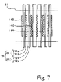
- FIG. 7 is a top view showing the array mode of the light emitting threads of the third embodiment of the present invention.
- FIG. 8 is a view showing the array mode of the light emitting threads in a fourth embodiment of the present invention.
- FIG. 1 Each embodiment to be described below, comparing with the related art ( FIGS. 1 to 3 ) described so far, is different only in the array structure of the fluorescent material layers on the boat and installation intervals of the pair of display electrodes. Consequently, in each embodiment to be described below also, the entire structure should be referred to FIG. 1 as it is, and here, the description will be focused on the characteristic portion of the present invention.
- FIG. 4 is a view showing the array structure of the fluorescent material layers on the boat, which is the fluorescent support member in the plasma tube array of a first embodiment of the present invention.
- a fluorescent layer 14 composed of sequentially lined up three types of the fluorescent material layers 14 R, 14 G, 14 B, 14 R, 14 G, 14 B . . . that emit each of the florescent lights of three colors of R, G, and B in the longitudinal direction of the boat 13 .
- These fluorescent material layers 14 R, 14 G, 14 B, 14 R, 14 G, 14 B . . . are formed in such a manner that an opened mask is arranged only on a portion where the fluorescent material intended to be coated so as to perform a screen printing, whereby the coated fluorescent material layers 14 R, 14 G, 14 B, . . . are formed on the boat 13 as shown in FIG. 4 .
- FIG. 5 is a view showing the light emitting threads of the first embodiment.
- the light emitting thread 10 shown here takes a glass tube 11 of 1 mm in diameter (0.1 mm in thickness) and 100 cm in total length and the boat 13 of 0.75 mm in width size as materials, and there are disposed in sequence therein the fluorescent material layers 14 R, 14 G, 14 B . . . that emit the fluorescent lights of red (R), green (G), blue (B) in this order on the boat 13 by using a screen printing technique at 0.3 mm width intervals in the longitudinal direction.
- the fluorescent material layers are referred to without classifying them into types, they are just collectively referred to as a fluorescent layer 14 .
- the boat 13 having thus disposed fluorescent layer 14 is put into a furnace so as to calcinate the fluorescent layer 14 , and after that, this boat 13 is put into the glass tube 11 formed with the MgO film 12 , and the discharge gas is enclosed into the glass tube 11 , and both ends of the glass tube 11 are sealed.
- the light emitting threads 10 thus formed are lined up, whereby the fluorescent material layers of the same type are adjacently lined up, and are held between and fixed by the front surface and the rear surface, for example, by the front surface support substrate and the rear surface support substrate such as glass substrates (not shown). From among these substrates, the front surface support substrate disposed in the front surface is formed with a pair of display electrodes 21 at 0.3 mm pitch intervals, and the pair of display electrodes 21 are aligned to the. arrangement of the fluorescent material layers inside the light emitting thread 10 .
- the signal electrodes 31 are formed, but the illustration thereof is omitted.
- the size of one pixel can be shrunk from the conventional size of 3 mm ⁇ 3 mm to the size of 1 mm ⁇ 1 mm, thereby achieving precision 9 times higher than the related art.
- the diameter (1 mm) of the glass tube 11 is the same as the size of the glass tube in the related art shown in FIG. 2 , and consequently, it can come off with the same extent of production, and though the number of steps of coating the fluorescent material layers onto the boat slightly increase, the production at almost the same level of cost can be performed.
- FIGS. 4 and 5 used for describing the first embodiment will be referred to as they are.
- a glass tube 11 of 2 mm in diameter (0.15 mm in thickness) and 100 cm in total length and a boat 13 of 1.6 mm in outer diameter are taken as materials, and, fluorescent material layers 14 R, 14 G, 14 B . . . are formed in order of red (R), green (G), blue (B) on the boat by using a dispense technique at 0.7 mm width intervals.
- Individual light emitting threads are formed by the same production step as the first embodiment, and are lined up, thereby fabricating a plasma tube array.
- one pixel is made highly precise toward the size of 2 mm ⁇ 2 mm, and at the same time, the diameter of the tube is made two times larger than that of the related art, so that a significant improvement of the strength is realized and the preparation of the light emitting threads becomes easy, and the strength and high precision which was conventionally in the relation of trade off become compatible.
- the parts are made large in size in this manner, between the fluorescent material layers 14 R, 14 G, 14 B . . . formed on the boat, there can be provided rib-shaped partitions, and when the fluorescent materials mounted on the same boat emit light, it is possible to make the fluorescent colors not mixed.
- FIGS. 6 and 7 are an oblique view and a top view showing the array mode of light emitting threads of the third embodiment of the present invention.
- Fluorescent material layers 14 R, 14 G, 14 B . . . provided in light emitting threads shown in FIGS. 6 and 7 are different in width in the alignment direction for each type, and as far as shown here, the width of the fluorescent material layer 14 G that emits the fluorescent light of green (G) is the most widest, and a pair of display electrodes 21 also become a pair of display electrodes having the width according to the size of the fluorescent material layer.
- the pair of display electrodes 21 similarly to each of the preceding examples, have two pieces of display electrodes 211 and 212 , and each of the display electrodes 211 and 212 is made up of bus electrodes 211 a and 212 a made of metal and transparent electrodes 211 b and 212 b .
- the pair of display electrodes 211 and 212 alone which correspond to the fluorescent material layer 14 G, show the transparent electrodes 211 b and 212 b , and for other display electrodes, the transparent electrodes are omitted to be shown.
- the fluorescent material layers 14 R, 14 G, 14 B . . . are different in light emitting efficiency for each type
- the fluorescent material layers 14 R, 14 G, 14 B . . . are different in width in the alignment direction for each type
- the light quantity of the fluorescent lights emitted from those fluorescent material layers 14 R, 14 G, 14 B . . . is adjusted to be at the same level for the image signal of the same level.
- FIG. 8 is a view showing an array mode of light emitting threads in the fourth embodiment of the present invention.
- the different points with the first embodiment described with reference to FIGS. 4 and 5 will be described.
- light emitting threads 10 of the same structure and preparing method as the previously described first embodiment are used, and in FIG. 8 , three pieces of light emitting threads adjacently lined up are shown.
- Each of the light emitting threads 10 has a boat 13 lined up in sequence with three types of the fluorescent material layers 14 R, 14 G, 14 B . . . inserted into glass tubes 11 in the longitudinal direction.
- the position of the boat 13 is shifted by 0.03 mm by adjacent light emitting thread, whereby three types of the fluorescent material layers 14 R, 14 G, 14 B . . . are lined up in sequence in the longitudinal direction of one piece of the light emitting thread 10 , and at the same time, three types of the fluorescent material layers 14 R, 14 G, 14 B . . . are also lined up in sequence across plural pieces of light emitting threads 10 in the extending direction of the pair of the display electrodes 21 .
- the fluorescent light colors controlled by the pair of display electrodes 211 and 212 become different in sequence depending on the light emitting threads 10 .
- the present disposition not only the resolution in x-y directions, but also the resolution in an oblique direction can be increased, and much higher image quality can be realized.
Abstract
Description
Claims (4)
Applications Claiming Priority (2)
| Application Number | Priority Date | Filing Date | Title |
|---|---|---|---|
| JP2005-84046 | 2005-03-23 | ||
| JP2005084046A JP2006269195A (en) | 2005-03-23 | 2005-03-23 | Plasma tube array and gas discharge tube |
Publications (2)
| Publication Number | Publication Date |
|---|---|
| US20060214554A1 US20060214554A1 (en) | 2006-09-28 |
| US7336027B2 true US7336027B2 (en) | 2008-02-26 |
Family
ID=37015586
Family Applications (1)
| Application Number | Title | Priority Date | Filing Date |
|---|---|---|---|
| US11/155,541 Expired - Fee Related US7336027B2 (en) | 2005-03-23 | 2005-06-20 | Plasma tube array and gas discharge tube |
Country Status (3)
| Country | Link |
|---|---|
| US (1) | US7336027B2 (en) |
| JP (1) | JP2006269195A (en) |
| CN (1) | CN100463017C (en) |
Families Citing this family (5)
| Publication number | Priority date | Publication date | Assignee | Title |
|---|---|---|---|---|
| CN101401144B (en) * | 2006-03-17 | 2010-12-01 | 筱田等离子有限公司 | Display device |
| WO2008096440A1 (en) * | 2007-02-08 | 2008-08-14 | Shinoda Plasma Co., Ltd. | Color display device and method for driving same |
| JP5047872B2 (en) * | 2008-04-30 | 2012-10-10 | 篠田プラズマ株式会社 | Gas discharge tube and display device |
| JP5189025B2 (en) * | 2008-06-18 | 2013-04-24 | 篠田プラズマ株式会社 | Display device |
| JP2011040271A (en) * | 2009-08-11 | 2011-02-24 | Shinoda Plasma Kk | Planar light source |
Citations (5)
| Publication number | Priority date | Publication date | Assignee | Title |
|---|---|---|---|---|
| JPS61103187A (en) | 1984-10-26 | 1986-05-21 | 富士通株式会社 | Large gas discharge display panel |
| US5514934A (en) * | 1991-05-31 | 1996-05-07 | Mitsubishi Denki Kabushiki Kaisha | Discharge lamp, image display device using the same and discharge lamp producing method |
| JP2003086141A (en) | 2001-09-12 | 2003-03-20 | Fujitsu Ltd | Gas discharge tube and display device using the same |
| JP2003272562A (en) | 2002-03-15 | 2003-09-26 | Fujitsu Ltd | Gas discharge tube and display device using the same |
| US7049748B2 (en) * | 2001-12-28 | 2006-05-23 | Fujitsu Limited | Display device employing gas discharge tubes arranged in parallel between front and rear substrates to comprise a display screen, each tube having a light emitting section as part of the display screen and a cleaning section connected to the light emitting section but displaced from the display screen |
Family Cites Families (6)
| Publication number | Priority date | Publication date | Assignee | Title |
|---|---|---|---|---|
| JPH05190153A (en) * | 1992-01-14 | 1993-07-30 | Mitsubishi Electric Corp | Luminous device and manufacture thereof |
| JPH10308179A (en) * | 1997-05-08 | 1998-11-17 | Matsushita Electric Ind Co Ltd | Plasma display panel, and its gradation display method |
| JPH1196923A (en) * | 1997-09-19 | 1999-04-09 | Fujitsu Ltd | Plasma display panel |
| JP2003045337A (en) * | 2001-07-31 | 2003-02-14 | Fujitsu Ltd | Display tube and display device |
| JP4909475B2 (en) * | 2001-09-13 | 2012-04-04 | 篠田プラズマ株式会社 | Display device |
| JP3877618B2 (en) * | 2002-03-15 | 2007-02-07 | 富士通株式会社 | Gas discharge tube and display device using the same |
-
2005
- 2005-03-23 JP JP2005084046A patent/JP2006269195A/en active Pending
- 2005-06-20 US US11/155,541 patent/US7336027B2/en not_active Expired - Fee Related
- 2005-07-14 CN CNB2005100841690A patent/CN100463017C/en not_active Expired - Fee Related
Patent Citations (5)
| Publication number | Priority date | Publication date | Assignee | Title |
|---|---|---|---|---|
| JPS61103187A (en) | 1984-10-26 | 1986-05-21 | 富士通株式会社 | Large gas discharge display panel |
| US5514934A (en) * | 1991-05-31 | 1996-05-07 | Mitsubishi Denki Kabushiki Kaisha | Discharge lamp, image display device using the same and discharge lamp producing method |
| JP2003086141A (en) | 2001-09-12 | 2003-03-20 | Fujitsu Ltd | Gas discharge tube and display device using the same |
| US7049748B2 (en) * | 2001-12-28 | 2006-05-23 | Fujitsu Limited | Display device employing gas discharge tubes arranged in parallel between front and rear substrates to comprise a display screen, each tube having a light emitting section as part of the display screen and a cleaning section connected to the light emitting section but displaced from the display screen |
| JP2003272562A (en) | 2002-03-15 | 2003-09-26 | Fujitsu Ltd | Gas discharge tube and display device using the same |
Also Published As
| Publication number | Publication date |
|---|---|
| CN1838201A (en) | 2006-09-27 |
| CN100463017C (en) | 2009-02-18 |
| US20060214554A1 (en) | 2006-09-28 |
| JP2006269195A (en) | 2006-10-05 |
Similar Documents
| Publication | Publication Date | Title |
|---|---|---|
| KR100727444B1 (en) | Display device | |
| US5825128A (en) | Plasma display panel with undulating separator walls | |
| US6677704B2 (en) | AC-type gas discharge display with elliptical discharge tube | |
| US5859508A (en) | Electronic fluorescent display system with simplified multiple electrode structure and its processing | |
| CN101563645B (en) | Screen structure for field emission device backlighting unit | |
| US7336027B2 (en) | Plasma tube array and gas discharge tube | |
| CN100538977C (en) | Plasmatron array | |
| KR100785563B1 (en) | Plasma display pannel | |
| US7623093B2 (en) | Array display apparatus | |
| EP1600997B1 (en) | Plasma display panel | |
| US20080024049A1 (en) | Plasma tube array | |
| EP1601000B1 (en) | Plasma display panel | |
| KR20030029697A (en) | Align mark and plasma display panel using the same | |
| JPH09129140A (en) | Plane discharge type plasma display panel | |
| US8330676B2 (en) | Plasma tube array-type display device and luminance correcting method | |
| CN209804581U (en) | plasma display screen | |
| CN100426346C (en) | Light-emitting array display device and driving method thereof | |
| US7459853B2 (en) | Plasma display panel for producing high color temperature white light and upper substrate thereof | |
| CN101164134A (en) | Color display | |
| CN100499014C (en) | Plasma display panel and a drive method therefor | |
| WO2006097974A1 (en) | Plasma tube array | |
| US20090146563A1 (en) | Plasma display panel and deposition apparatus used in the manufacturing thereof | |
| EP2144268A1 (en) | Plasma display panel | |
| CN101180701A (en) | Plasmatron array | |
| CN1971813A (en) | Plasma display panel |
Legal Events
| Date | Code | Title | Description |
|---|---|---|---|
| AS | Assignment |
Owner name: FUJITSU LIMITED, JAPAN Free format text: ASSIGNMENT OF ASSIGNORS INTEREST;ASSIGNORS:YAMAZAKI, YOSUKE;ISHIMOTO, MANABU;YAMADA, HITOSHI;AND OTHERS;REEL/FRAME:016706/0025;SIGNING DATES FROM 20050607 TO 20050608 |
|
| AS | Assignment |
Owner name: SHINODA PLASMA CORPORATION, JAPAN Free format text: ASSIGNMENT OF ASSIGNORS INTEREST;ASSIGNOR:FUJITSU LIMITED;REEL/FRAME:019529/0562 Effective date: 20070501 Owner name: SHINODA PLASMA CORPORATION,JAPAN Free format text: ASSIGNMENT OF ASSIGNORS INTEREST;ASSIGNOR:FUJITSU LIMITED;REEL/FRAME:019529/0562 Effective date: 20070501 |
|
| AS | Assignment |
Owner name: SHINODA PLASMA CORPORATION, JAPAN Free format text: ASSIGNMENT OF ASSIGNORS INTEREST;ASSIGNOR:FUJITSU LIMITED;REEL/FRAME:019632/0424 Effective date: 20070501 |
|
| FEPP | Fee payment procedure |
Free format text: PAYOR NUMBER ASSIGNED (ORIGINAL EVENT CODE: ASPN); ENTITY STATUS OF PATENT OWNER: LARGE ENTITY |
|
| FPAY | Fee payment |
Year of fee payment: 4 |
|
| AS | Assignment |
Owner name: TOPPAN PRINTING CO., LTD., JAPAN Free format text: LIEN;ASSIGNOR:SHINODA PLASMA CORP.;REEL/FRAME:031522/0436 Effective date: 20130821 |
|
| REMI | Maintenance fee reminder mailed | ||
| LAPS | Lapse for failure to pay maintenance fees | ||
| STCH | Information on status: patent discontinuation |
Free format text: PATENT EXPIRED DUE TO NONPAYMENT OF MAINTENANCE FEES UNDER 37 CFR 1.362 |
|
| FP | Lapsed due to failure to pay maintenance fee |
Effective date: 20160226 |