US7352269B2 - Method for making magnetic components with N-phase coupling, and related inductor structures - Google Patents
Method for making magnetic components with N-phase coupling, and related inductor structures Download PDFInfo
- Publication number
- US7352269B2 US7352269B2 US10/318,896 US31889602A US7352269B2 US 7352269 B2 US7352269 B2 US 7352269B2 US 31889602 A US31889602 A US 31889602A US 7352269 B2 US7352269 B2 US 7352269B2
- Authority
- US
- United States
- Prior art keywords
- coupled inductor
- windings
- magnetic
- phase coupled
- phase
- Prior art date
- Legal status (The legal status is an assumption and is not a legal conclusion. Google has not performed a legal analysis and makes no representation as to the accuracy of the status listed.)
- Expired - Lifetime, expires
Links
- 230000005291 magnetic effect Effects 0.000 title claims abstract description 189
- 230000008878 coupling Effects 0.000 title claims description 32
- 238000010168 coupling process Methods 0.000 title claims description 32
- 238000005859 coupling reaction Methods 0.000 title claims description 32
- 238000000034 method Methods 0.000 title abstract description 16
- 238000004804 winding Methods 0.000 claims description 211
- 239000000696 magnetic material Substances 0.000 claims 8
- 230000004907 flux Effects 0.000 claims 4
- 238000000926 separation method Methods 0.000 claims 4
- 230000008901 benefit Effects 0.000 abstract description 19
- 238000010276 construction Methods 0.000 abstract description 4
- DHDBTLFALXRTLB-UHFFFAOYSA-N 1,2,5-trichloro-3-(3-chlorophenyl)benzene Chemical compound ClC1=CC=CC(C=2C(=C(Cl)C=C(Cl)C=2)Cl)=C1 DHDBTLFALXRTLB-UHFFFAOYSA-N 0.000 description 8
- YAHNWSSFXMVPOU-UHFFFAOYSA-N 2,3',4,4',5'-Pentachlorobiphenyl Chemical compound ClC1=CC(Cl)=CC=C1C1=CC(Cl)=C(Cl)C(Cl)=C1 YAHNWSSFXMVPOU-UHFFFAOYSA-N 0.000 description 7
- 230000009467 reduction Effects 0.000 description 7
- 238000004519 manufacturing process Methods 0.000 description 6
- YDGFMDPEJCJZEV-UHFFFAOYSA-N 1,2,4-trichloro-3-(3,5-dichlorophenyl)benzene Chemical compound ClC1=CC(Cl)=CC(C=2C(=C(Cl)C=CC=2Cl)Cl)=C1 YDGFMDPEJCJZEV-UHFFFAOYSA-N 0.000 description 5
- 230000010354 integration Effects 0.000 description 5
- UHCLFIWDCYOTOL-UHFFFAOYSA-N 1,2,4,5-tetrachloro-3-(2,5-dichlorophenyl)benzene Chemical compound ClC1=CC=C(Cl)C(C=2C(=C(Cl)C=C(Cl)C=2Cl)Cl)=C1 UHCLFIWDCYOTOL-UHFFFAOYSA-N 0.000 description 4
- LAHWLEDBADHJGA-UHFFFAOYSA-N 1,2,4-trichloro-5-(2,5-dichlorophenyl)benzene Chemical compound ClC1=CC=C(Cl)C(C=2C(=CC(Cl)=C(Cl)C=2)Cl)=C1 LAHWLEDBADHJGA-UHFFFAOYSA-N 0.000 description 4
- 230000005294 ferromagnetic effect Effects 0.000 description 3
- 230000006870 function Effects 0.000 description 3
- 238000004364 calculation method Methods 0.000 description 2
- 238000006243 chemical reaction Methods 0.000 description 2
- 239000003302 ferromagnetic material Substances 0.000 description 2
- 239000000843 powder Substances 0.000 description 2
- 230000004044 response Effects 0.000 description 2
- UXUFTKZYJYGMGO-CMCWBKRRSA-N (2s,3s,4r,5r)-5-[6-amino-2-[2-[4-[3-(2-aminoethylamino)-3-oxopropyl]phenyl]ethylamino]purin-9-yl]-n-ethyl-3,4-dihydroxyoxolane-2-carboxamide Chemical compound O[C@@H]1[C@H](O)[C@@H](C(=O)NCC)O[C@H]1N1C2=NC(NCCC=3C=CC(CCC(=O)NCCN)=CC=3)=NC(N)=C2N=C1 UXUFTKZYJYGMGO-CMCWBKRRSA-N 0.000 description 1
- RYGMFSIKBFXOCR-UHFFFAOYSA-N Copper Chemical compound [Cu] RYGMFSIKBFXOCR-UHFFFAOYSA-N 0.000 description 1
- 239000004642 Polyimide Substances 0.000 description 1
- 230000009286 beneficial effect Effects 0.000 description 1
- -1 by flat portions 50P Chemical compound 0.000 description 1
- 239000003990 capacitor Substances 0.000 description 1
- 239000004020 conductor Substances 0.000 description 1
- 239000013256 coordination polymer Substances 0.000 description 1
- 229910052802 copper Inorganic materials 0.000 description 1
- 239000010949 copper Substances 0.000 description 1
- 238000005516 engineering process Methods 0.000 description 1
- 230000017525 heat dissipation Effects 0.000 description 1
- 230000003993 interaction Effects 0.000 description 1
- 230000013011 mating Effects 0.000 description 1
- 230000003071 parasitic effect Effects 0.000 description 1
- 230000035699 permeability Effects 0.000 description 1
- 229920001721 polyimide Polymers 0.000 description 1
- 230000008569 process Effects 0.000 description 1
- 230000035945 sensitivity Effects 0.000 description 1
- 229910000679 solder Inorganic materials 0.000 description 1
- 238000005476 soldering Methods 0.000 description 1
- 239000007787 solid Substances 0.000 description 1
- 239000010409 thin film Substances 0.000 description 1
- 230000001052 transient effect Effects 0.000 description 1
Images


Classifications
-
- H—ELECTRICITY
- H02—GENERATION; CONVERSION OR DISTRIBUTION OF ELECTRIC POWER
- H02M—APPARATUS FOR CONVERSION BETWEEN AC AND AC, BETWEEN AC AND DC, OR BETWEEN DC AND DC, AND FOR USE WITH MAINS OR SIMILAR POWER SUPPLY SYSTEMS; CONVERSION OF DC OR AC INPUT POWER INTO SURGE OUTPUT POWER; CONTROL OR REGULATION THEREOF
- H02M1/00—Details of apparatus for conversion
- H02M1/14—Arrangements for reducing ripples from dc input or output
-
- H—ELECTRICITY
- H01—ELECTRIC ELEMENTS
- H01F—MAGNETS; INDUCTANCES; TRANSFORMERS; SELECTION OF MATERIALS FOR THEIR MAGNETIC PROPERTIES
- H01F17/00—Fixed inductances of the signal type
- H01F17/04—Fixed inductances of the signal type with magnetic core
-
- H—ELECTRICITY
- H01—ELECTRIC ELEMENTS
- H01F—MAGNETS; INDUCTANCES; TRANSFORMERS; SELECTION OF MATERIALS FOR THEIR MAGNETIC PROPERTIES
- H01F37/00—Fixed inductances not covered by group H01F17/00
-
- H—ELECTRICITY
- H02—GENERATION; CONVERSION OR DISTRIBUTION OF ELECTRIC POWER
- H02M—APPARATUS FOR CONVERSION BETWEEN AC AND AC, BETWEEN AC AND DC, OR BETWEEN DC AND DC, AND FOR USE WITH MAINS OR SIMILAR POWER SUPPLY SYSTEMS; CONVERSION OF DC OR AC INPUT POWER INTO SURGE OUTPUT POWER; CONTROL OR REGULATION THEREOF
- H02M3/00—Conversion of dc power input into dc power output
- H02M3/003—Constructional details, e.g. physical layout, assembly, wiring or busbar connections
-
- H—ELECTRICITY
- H02—GENERATION; CONVERSION OR DISTRIBUTION OF ELECTRIC POWER
- H02M—APPARATUS FOR CONVERSION BETWEEN AC AND AC, BETWEEN AC AND DC, OR BETWEEN DC AND DC, AND FOR USE WITH MAINS OR SIMILAR POWER SUPPLY SYSTEMS; CONVERSION OF DC OR AC INPUT POWER INTO SURGE OUTPUT POWER; CONTROL OR REGULATION THEREOF
- H02M7/00—Conversion of ac power input into dc power output; Conversion of dc power input into ac power output
- H02M7/003—Constructional details, e.g. physical layout, assembly, wiring or busbar connections
Definitions
- the invention relates generally to making DC-to-DC converters. More specifically the invention relates to construction of a coupled inductor within a multi-phase DC-to-DC converter.
- a DC-to-DC converter provides an output voltage that is a step-up, a step-down, or a polarity reversal of the input voltage source.
- Certain known DC-to-DC converters have parallel power units with inputs coupled to a common DC voltage source and outputs coupled to a load, such as a microprocessor. Multiple power-units can sometimes reduce cost by lowering the power and size rating of components. A further benefit is that multiple power units provide smaller per-power-unit peak current levels, combined with smaller passive components.
- the prior art also includes switching techniques in parallel-power-unit DC-to-DC converters.
- power units may be switched with pulse width modulation (PWM) or with pulse frequency modulation (PFM).
- PWM pulse width modulation
- PFM pulse frequency modulation
- a parallel-unit buck converter the energizing and de-energizing of the inductance in each power unit occurs out of phase with switches coupled to the input, inductor and ground. Additional performance benefits are provided when the switches of one power unit, coupling the inductors to the DC input voltage or to ground, are out of phase with respect to the switches in another power unit.
- Such a “multi-phase,” parallel power unit technique results in ripple current cancellation at a capacitor, to which all the inductors are coupled at their respective output terminals.
- the '986 patent shows one system that reduces the ripple of the inductor current in a two-phase coupled inductor within a DC-to-DC buck converter.
- the '986 patent also provides a multi-phase transformer model to illustrate the working principles of multi-phase coupled inductors. It is a continuing problem to address scalability and implementation issues DC-to-DC converters.
- DC-to-DC converter As circuit components and, thus, printed circuit boards (PCB), become smaller due to technology advancements, smaller and more scalable DC-to-DC converters are needed to provide for a variety of voltage conversion needs.
- One specific feature presented hereinafter is to provide a DC-to-DC converter, the DC-to-DC converter being scalable in some embodiments.
- Another feature is to provide a converter that is mountable to a PCB.
- Yet another feature is to provide a lower cost manufacturing methodology for DC-to-DC converters, as compared to the prior art.
- Coupled inductors described herein may be used within DC-to-DC converters or within a power converter for power conversion applications, for example.
- a method of one aspect provides for constructing a magnetic core.
- a magnetic core is, for example, useful in applications detailed in the '986 patent.
- the method provides for constructing N-phase coupled inductors as both single and scalable magnetic structures, where N is greater than 1.
- An N-phase inductor as described herein may include N-number of windings.
- One method additionally describes construction of a magnetic core that enhances the benefits of using the scalable N-phase coupled inductor.
- the N-phase coupled inductor is formed by coupling first and second magnetic cores in such a way that a planar surface of the first core is substantially aligned with a planar surface of the second core in a common plane.
- the first and second magnetic cores may be formed into shapes that, when coupled together, may form a single scalable magnetic core having desirable characteristics, such as ripple current reduction and ease of implementation.
- the cores are fashioned into shapes, such as a U-shape, an I-shape (e.g., a bar), an H-shape, a ring-shape, a rectangular-shape, or a comb.
- the cores could be fashioned into a printed circuit trace within a PCB.
- certain cores form passageways through which conductive windings are wound when coupled together.
- Other cores may already form these passageways (e.g., the ring-shaped core and the rectangularly shaped core).
- two H-shaped magnetic cores may be coupled at the legs of each magnetic core to form a passageway.
- a multi-leg core may be formed as a comb-shaped core coupled to an I-shaped core.
- two I-shaped cores are layered about a PCB such that passageways are formed when the two cores are coupled to one another at two or more places, or when pre-configured holes in the PCB are filled with a ferromagnetic powder.
- Advantages of the method and structures herein include a scalable and cost effective DC-to-DC converter that reduces or nearly eliminates ripple current.
- the methods and structures further techniques that achieve the benefit of various performance characteristics with a single, scalable, topology.
- FIG. 1 shows one multi-phase DC-to-DC converter system
- FIG. 2 shows one two-phase coupled inductor
- FIG. 3 shows one two-phase coupled ring-core inductor
- FIG. 4 shows one vertically mounted two-phase coupled inductor
- FIG. 5 shows one plate structured two-phase coupled inductor
- FIG. 6 shows one scalable multi-phase coupled inductor with H-shaped cores
- FIG. 7 shows one scalable multi-phase coupled inductor with rectangular-shaped cores
- FIG. 8 shows one scalable multi-phase coupled inductor with U-shaped cores
- FIG. 9 shows one integrated multi-phase coupled inductor with a comb-shaped core
- FIG. 10 shows one scalable multi-phase coupled inductor with combinations of shaped cores
- FIG. 11 shows one scalable multi-phase coupled inductor with “staple” cores
- FIG. 12 shows an assembly view of the coupled inductor of FIG. 11 ;
- FIG. 13 shows a surface view of the inductor of FIG. 11 ;
- FIG. 14 shows one scaleable coupled inductor with bar magnet cores
- FIG. 15 shows one multi-phase coupled inductor with through-board integration
- FIG. 16 shows another multi-phase coupled inductor with through-board integration
- FIG. 17 shows one scalable multi-phase coupled ring-core inductor.
- FIG. 1 shows a multi-phase DC-to-DC converter system 10 .
- Each switch and inductor pair 14 , 24 represent one phase 26 of system 10 , as shown.
- Inductors 24 cooperate together as a coupled inductor 28 .
- Power source 12 may, for example, be either a DC power source, such as a battery, or an AC power source cooperatively coupled to a rectifier, such as a bridge rectifier, to provide DC power in signal 18 .
- Each switch 14 may include a plurality of switches to perform the functions of DC-to-DC converter system 10 .
- DC-to-DC converter system 10 converts an input signal 18 from source 12 to an output signal 30 .
- the voltage of signal 30 may be controlled through operation of switches 14 , to be equal to or different from signal 18 .
- coupled inductor 28 has one or more windings (not shown) that extend through and about inductors 24 , as described in detail below. These windings attach to switches 14 , which collectively operate to regulate the output voltage of signal 30 by sequentially switching inductors 24 to signal 18 .
- system 10 may for example be used as a two-phase power converter, (e.g., power supply).
- System 10 may also be used in both DC and AC based power supplies to replace a plurality of individual discrete inductors such that coupled inductor 28 reduces inductor ripple current, filter capacitances, and/or PCB footprint sizes, while delivering higher system efficiency and enhanced system reliability.
- Other functional and operational aspects of DC-to-DC converter system 10 may be exemplarily described in the '986 patent, features of coupled inductor 28 are described in detail below in connection with FIG. 2-FIG . 17 .
- system 10 may be arranged with different topologies to provide a coupled inductor 28 and without departing from the scope hereof.
- FIG. 2 shows a two-phase coupled inductor 33 , in accord with one embodiment.
- the two-phase coupled inductor 33 may include a first magnetic core 36 A and a second magnetic core 36 B.
- the first and second magnetic cores 36 A, 36 B, respectively, are coupled together such that planar surfaces 37 A, 37 B, respectively, of each core are substantially aligned in a common plane, represented by line 35 .
- the two magnetic cores 36 A and 36 B are coupled together, they cooperatively form a single magnetic core for use as a two-phase coupled inductor 33 .
- the first magnetic core 36 A may be formed from a ferromagnetic material into a U-shape.
- the second magnetic core 36 B may be formed from the same ferromagnetic material into a bar, or I-shape, as shown.
- the windings 34 A, 34 B may be formed of a conductive material, such as copper, that wind though and about the passageway 38 and the magnetic core 36 B.
- windings 34 A, 34 B may include a same or differing number of turns about the magnetic core 36 B. Windings 34 A, 34 B are shown as single turn windings, to decrease resistance through inductor 33 .
- the windings 34 A and 34 B of inductor 33 may be wound in the same or different orientation from one another.
- the windings 34 A and 34 B may also be either wound about the single magnetic core in the same number of turns or in a different number of turns.
- the number of turns and orientation of each winding may be selected so as to support the functionality of the '986 patent, for example.
- a gap may exist between magnetic cores 36 A, 36 B, for example to reduce the sensitivity to direct current when inductor 33 is used within a switching power converter.
- Such a gap is for example illustratively discussed as dimension A, FIG. 5 .
- the dimensional distance between windings 34 A, 34 B may also be adjusted to adjust leakage inductance. Such a dimension is illustratively discussed as dimension E, FIG. 5 .
- magnetic core 36 A is a “U-shaped” core while magnetic core 36 B is an unshaped flat plate.
- coupled inductor 33 may be formed with magnetic cores with different shapes.
- two “L-shaped” or two “U-shaped” cores may be coupled together to provide like overall form as combined cores 36 A, 36 B, to provide like functionality within a switching power converter.
- Cores 36 A, 36 B may be similarly replaced with a solid magnetic core block with a hole therein to form passageway 38 .
- At least part of passageway 38 is free from intervening magnetic structure between windings 34 A, 34 B; air or non-magnetic structure may for example fill the space of passageway 38 and between the windings 34 A, 34 B.
- intervening magnetic structure fills no more than 50% of a cross-sectional area between windings 34 A, 34 B, and within passageway 38 ; by way of example, the cross-sectional area of passageway 38 may be defined by the plane of dimensions 39 A, 39 B, which is perpendicular to a line 39 C between windings 34 A, 34 B.
- FIG. 2 also illustrates one advantageous feature associated with windings 34 A, 34 B. Specifically, each of windings 34 A, 34 B is shown with a rectangular cross-section that, when folded underneath core 36 B, as shown, produces a tab for soldering to a PCB, and without the need for a separate item. Other windings discussed below may have similar beneficial features.
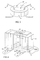
- FIG. 3 shows a single two-phase ring-core coupled inductor 43 , in accord with one embodiment.
- Inductor 43 may be combined with other embodiments herein, for example, to serve as inductor 28 of FIG. 1 .
- the ring-core inductor 43 is formed from a ring magnetic core 44 .
- the core 44 has a passageway 45 ; windings 40 and 42 are wound through passageway 45 and about the core 44 , as shown.
- core 44 is formed as a single magnetic core; however multiple magnetic cores, such as two semi-circles, may be cooperatively combined to form a similar core structure.
- Other single magnetic core embodiments shown herein may also be formed by cooperatively combining multiple magnetic cores as discussed in FIG. 17 .
- Such a combination may align plane 44 P of magnetic core 44 in the same plane of other magnetic cores 44 , for example to facilitate mounting to a PCB.
- At least part of passageway 45 is free from intervening magnetic structure between windings 40 , 42 ; air may for example fill the space of passageway 45 and between windings 40 , 42 .
- intervening magnetic structure fills no more than 50% of a cross-sectional area between windings 40 , 42 , and within passageway 45 .
- windings 40 , 42 wind through passageway 45 and around ring magnetic core 44 such that ring magnetic core 44 and windings 40 , 42 cooperate with two phase coupling within a switching power converter.
- Winding 40 is oriented such dc current in winding 40 flows in a first direction within passageway 45 ; winding 42 is oriented such that dc current in winding 42 flows in a second direction within passageway 45 , where the first direction is opposite to the second direction.
- Such a configuration avoids dc saturation of core 44 , and effectively reduces ripple current. See U.S. Pat. No. 6,362,986.
- FIG. 4 shows a vertically mounted two-phase coupled inductor 54 , in accord with one embodiment.
- Inductor 54 may be combined and/or formed with other embodiments herein, for example, to serve as inductor 28 of FIG. 1 .
- the inductor 54 is formed as a rectangular-shaped magnetic core 55 .
- the core 55 forms a passageway 56 ; windings 50 and 52 may be wound through passageway 56 and about the core 55 .
- the inductor 54 may be vertically mounted on a plane of PCB 57 (e.g., one end of passageway 56 faces the plane of the PCB 57 ) so as to minimize a “footprint”, or real estate, occupied by the inductor 54 on the PCB 57 .
- This embodiment may improve board layout convenience.
- Windings 50 and 52 may connect to printed traces 59 A, 59 B on the PCB 57 for receiving current. Additionally, windings 50 and 52 may be used to mount inductor 54 to the PCB 57 , such as by flat portions 50 P, 52 P of respective windings 50 , 52 . Specifically, portions 50 P, 52 P may be soldered underneath to PCB 57 . At least part of passageway 56 is free from intervening magnetic structure between windings 50 , 52 ; air may for example fill the space of passageway 56 and between windings 50 , 52 .
- intervening magnetic structure fills no more than 50% of a cross-sectional area between windings 50 , 52 , and within passageway 56 ; by way of example, the cross-sectional area of passageway 56 may be defined by the plane of dimensions 53 A, 53 B, which is perpendicular to a line 53 C between windings 50 , 52 .
- FIG. 4 further has advantages in that one winding 50 winds around one side of core 55 , while winding 52 winds around another side of core 55 , as shown.
- Such a configuration thus provides for input on one side of inductor 54 and output on the other side with convenient mating to a board layout of PCB 57 .
- FIG. 5 shows a two-phase coupled inductor 60 , in accord with one embodiment.
- Inductor 60 may, for example, serve as inductor 28 of FIG. 1 .
- the inductor 60 may be formed from first and second magnetic cores 61 and 62 , respectively.
- the illustration of the cores 61 and 62 is exaggerated for the purpose of showing detail of inductor 60 .
- the two cores 61 and 62 may be “sandwiched” about the windings 64 and 63 .
- the dimensions E, C and A are part of the calculation that determines a leakage inductance for inductor 60 .
- D, C, and A are part of the calculation that determines a magnetizing inductance of the inductor 60 .
- dimension D is much greater than E
- equations for leakage inductance and magnetizing inductance can be approximated as:
- ⁇ 0 is the permeability of free space
- L 1 is leakage inductance
- L m is magnetizing inductance.
- the cores 61 and 62 may be formed as conductive prints, or traces, directly with a PCB, thereby simplifying assembly processes of circuit construction such that windings 63 , 64 are also PCB traces that couple through one or more planes of a multi-plane PCB.
- the two-phase inductor 60 may be implemented on a PCB as two parallel thin-film magnetic cores 61 and 62 .
- inductor 60 may form planar surfaces 63 P and 64 P of respective windings 63 , 64 to facilitate mounting of inductor 60 onto the PCB.
- Dimensions E, A between windings 63 , 64 may define a passageway through inductor 60 .
- this passageway is free from intervening magnetic structure between windings 63 , 64 ; air may for example fill the space of the passageway and between windings 63 , 64 .
- intervening magnetic structure fills no more than 50% of a cross-sectional area between windings 63 , 64 , and within the passageway; by way of example, the cross-sectional area of the passageway may be defined by the plane of dimensions A, C, which is perpendicular to a line parallel to dimension E between windings 63 , 64 .
- FIG. 6 shows a scalable, multi-phase coupled inductor 70 that may be formed from a plurality of H-shaped magnetic cores 74 , in accord with one embodiment.
- Inductor 70 may, for example, serve as inductor 28 of FIG. 1 .
- the inductor 70 may be formed by coupling “legs” 74 A of each H-shaped core 74 together.
- Each core 74 has one winding 72 .
- the windings 72 may be wound through the passageways 71 formed by legs 74 A of each core 74 .
- the winding of each core 74 may be wound prior to coupling the several cores together such that manufacturing of inductor 70 is simplified.
- cores 74 may be made and used later; if a design requires additional phases, more of the cores 74 may be coupled together “as needed” without having to form additional windings 72 .
- Each core 74 may be mounted on a PCB, such as PCB 57 of FIG. 4 , and be coupled together to implement a particular design.
- One advantage to inductor 70 is that a plurality of cores 74 may be coupled together to make a multi-core inductor that is scalable.
- H-shaped cores 74 cooperatively form a four-phase coupled inductor. Other embodiments may, for example, scale the number of phases of the inductor 70 by coupling more H-shaped cores 74 .
- the coupling of another H-shaped core 74 may increase the number of phases of the inductor 70 to five.
- the center posts 74 C about which the windings 72 are wound may be thinner (along direction D) than the legs 74 A (along direction D). Thinner center posts 74 C may reduce winding resistance and increase leakage inductance without increasing the footprint size of the coupled inductor 70 .
- Each of the H-shaped cores 74 has a planar surface 74 P, for example, that aligns with other H-shaped cores in the same plane and facilitates mounting of inductor 70 onto PCB 74 S.
- At least part of one passageway 71 is free from intervening magnetic structure between windings 72 ; for example air may fill the three central passageways 71 of inductor 70 and between windings 72 in those three central passageways 71 .
- intervening magnetic structure fills no more than 50% of a cross-sectional area between windings 72 , and within passageway 71 .
- FIG. 7 shows a scalable, multi-phase coupled inductor 75 formed from a plurality of U-shaped magnetic cores 78 and an equal number of I-shaped magnetic cores 79 (e.g., bars), in accord with one embodiment.
- Inductor 75 may, for example, serve as inductor 28 of FIG. 1 .
- the U-shaped cores 78 coupled with the I-shaped cores 79 may form rectangular-shaped core cells 75 A, 75 B, 75 C, and 75 D, each of which is similar to the cell of FIG. 2 , but for the winding placement.
- the inductor 75 may be formed by coupling each of the rectangular-shaped core cells 75 A, 75 B, 75 C, and 75 D together.
- the windings 76 and 77 may be wound through the passageways (labeled “APERTURE”) formed by the couplings of cores 78 with cores 79 and about core elements. Similar to FIG. 6 , the windings 76 and 77 of each rectangular-shaped core cell may be made prior to coupling with other rectangular-shaped core cells 75 A, 75 B, 75 C, and 75 D such that manufacturing of inductor 75 is simplified; additional inductors 75 , may thus, be implemented “as needed” in a design.
- One advantage to inductor 75 is that cells 75 A, 75 B, 75 C, and 75 D—and/or other like cells—may be coupled together to make inductor 75 scalable. In the illustrated embodiment of FIG.
- each of the I-shaped cores 79 has a planar surface 79 P, for example, that aligns with other I-shaped cores in the same plane and facilitates mounting of inductor 75 onto PCB 79 S.
- At least part of the Apertures is free from intervening magnetic structure between windings 76 , 77 ; air may for example fill the space of these passageways and between windings 76 , 77 .
- each Aperture is shown with a pair of windings 76 , 77 passing therethrough, with only air filling the space between the windings 76 , 77 .
- intervening magnetic structure fills no more than 50% of a cross-sectional area between windings 76 , 77 , and within each respective Aperture.
- FIG. 8 shows a scalable, multi-phase coupled inductor 80 formed from a plurality of U-shaped magnetic cores 81 (or C-shaped depending on the orientation), in accord with one embodiment.
- Each magnetic core 81 has two lateral members 81 L and an upright member 81 U, as shown.
- Inductor 80 may, for example, serve as inductor 28 of FIG. 1 .
- the inductor 80 may be formed by coupling lateral members 81 L of each U-shaped core 81 (except for the last core 81 in a row) together with the upright member 81 U of a succeeding U-shaped core 81 , as shown.
- the windings 82 and 83 may be wound through the passageways 84 formed between each pair of cores 81 .
- winding 82 and its respective core 81 may be identical to winding 83 and its respective core 81 , forming a pair of like cells. More cells can be added to desired scalability.
- Each of the U-shaped cores 81 has a planar surface 81 P, for example, that aligns with other U-shaped cores 81 in the same plane and facilitates mounting of inductor 80 onto PCB 81 S.
- At least part of one passageway 84 is free from intervening magnetic structure between windings 82 , 83 ; air may for example fill the space of this passageway 84 and between windings 82 , 83 .
- passageways 84 are shown each with a pair of windings 82 , 83 passing therethrough, with only air filling the space between the windings 82 , 83 .
- One winding 82 is at the end of inductor 80 and does not pass through such a passageway 84 ; and another winding 83 is at another end of inductor 80 and does not pass through such a passageway 84 .
- intervening magnetic structure fills no more than 50% of a cross-sectional area between windings 82 , 83 , and within passageway 84 .
- FIG. 9 shows a multi-phase coupled inductor 85 formed from a comb-shaped magnetic core 86 and an I-shaped (e.g., a bar) magnetic core 87 , in accord with one embodiment.
- Inductor 85 may, for example, serve as inductor 28 of FIG. 1 .
- the inductor 85 may be formed by coupling a planar surface 86 P of “teeth” 86 A of the comb-shaped core 86 to a planar surface 87 P of the I-shaped core 87 in substantially the same plane.
- the windings 88 and 89 may be wound through the passageways 86 B formed by adjacent teeth 86 A of comb-shaped core 86 as coupled with I-shaped core 87 .
- FIG. 9 also shows end passageways 200 , planar surfaces 202 , 204 , 206 , 208 , 210 , 212 , 214 , and 224 , height 216 , depth 218 , and widths 220 and 220 .
- This embodiment may also be scalable by coupling inductor 85 with other inductor structures shown herein.
- the U-shaped magnetic cores 81 of FIG. 8 may be coupled to inductor 85 to form a multi-phase inductor, or a N+1 phase inductor.
- the I-shaped core 87 has a planar surface 87 P, for example, that facilitates mounting of inductor 85 onto PCB 87 S. At least part of one passageway 86 B is free from intervening magnetic structure between windings 88 , 89 ; air may for example fill the space of this passageway 86 B and between windings 88 , 89 .
- three passageways 86 B are shown each with a pair of windings 88 , 89 passing therethrough, with only air filling the space between the windings 88 , 89 .
- intervening magnetic structure fills no more than 50% of a cross-sectional area between windings 88 , 89 , and within passageway 86 B.
- windings 88 , 89 wind around teeth 86 A of core 86 , rather than around I-shaped core 87 or the non-teeth portion of core 86 .
- FIG. 10 shows a scalable, multi-phase coupled inductor 90 that may be formed from a comb-shaped magnetic core 92 and an I-shaped (e.g., a bar) magnetic core 93 , in accord with one embodiment.
- Inductor 90 may, for example, serve as inductor 28 of FIG. 1 .
- the inductor 90 may be formed by coupling “teeth” 92 A of the comb-shaped core 92 to the I-shaped core 93 , similar to FIG. 8 .
- the inductor 90 may be scaled to include more phases by the addition of the one more core cells to form a scalable structure.
- H-shaped cores 91 (such as those shown in FIG.
- H-shaped magnetic cores 74 may be coupled to cores 92 and 93 , as shown.
- the windings 94 and 95 may be wound through the passageways 90 A formed by the teeth 92 A as coupled with I-shaped core 93 .
- the windings 94 and 95 may be wound about the teeth 92 A of core 92 and the “bars” 91 A of H-shaped cores 91 .
- Scalability and ease of manufacturing advantages are similar to those previously mentioned. Those skilled in the art should appreciate that other shapes, such as the U-shaped cores and rectangular shaped cores, may be formed similarly to cores 92 and 93 .
- Each of the I-shaped core 92 and the H-shaped cores 91 has a respective planar surface 92 P and 91 P, for example, that aligns in the same plane and facilitates mounting of inductor 90 onto PCB 90 S.
- At least part of one passageway 90 A is free from intervening magnetic structure between windings 94 , 95 ; air may for example fill the space of this passageway 90 A and between windings 94 , 95 .
- five passageways 90 A are shown each with a pair of windings 94 , 95 passing therethrough, with only air filling the space between the windings 94 , 95 .
- intervening magnetic structure fills no more than 50% of a cross-sectional area between windings 94 , 95 , and within passageway 90 A.
- FIGS. 11-13 show staple magnetic cores 102 that may serve to implement a scalable multi-phase coupled inductor 100 .
- Inductor 100 may, for example, serve as inductor 28 of FIG. 1 .
- the staple magnetic cores 102 are, for example, U-shaped and may function similar to a “staple”.
- the staple magnetic cores 102 may connect, or staple, through PCB 101 to bus bars 103 to form a plurality of magnetic core cells.
- the two bus bars 103 may be affixed to one side of PCB 101 such that the staple magnetic cores 102 traverse through the PCB 101 from the opposite side of the PCB to physically couple to the bus bars 103 .
- One staple magnetic core may implement a single phase for the inductor 100 ; thus the inductor 100 may be scalable by adding more of staple magnetic cores 101 and windings 104 , 105 .
- a two-phase coupled inductor would have two staple magnetic cores 102 coupled to bus bars 103 with each core having a winding, such as windings 104 , 105 ; the number of phases are thus equal to the number of staple magnetic cores 102 and windings 104 , 105 .
- inductor 100 FIG. 11 , shows a 3-phase inductor.
- Advantages of this embodiment provide a PCB structure that may be designed in layout. As such, PCB real estate determinations may be made with fewer restrictions, as the inductor 100 becomes part of the PCB design.
- FIG. 13 Other advantages of the embodiment are apparent in FIG. 13 .
- the staples 102 may connect to PCB 101 at angles to each PCB trace (i.e., windings 104 and 105 ) so as to not incur added resistance while at the same time improving adjustability of leakage inductance. For example, extreme angles, such as 90 degrees, may increase the overall length of a PCB trace, which in turn increases resistance due to greater current travel. Further advantages of this embodiment include the reduction or avoidance of solder joints, which can significantly diminish high current. Additionally, the embodiment may incur fewer or no additional winding costs as the windings are part of the PCB; this may improve dimensional control so as to provide consistent characteristics such as AC resistance and leakage inductance.
- FIG. 14 shows bar magnetic cores 152 , 153 that serve to implement a scalable coupled inductor 150 .
- Inductor 150 may, for example, serve as inductor 28 of FIG. 1 .
- the bar magnetic cores 152 , 153 are, for example, respectively mounted to opposing sides 156 , 157 of PCB 151 .
- Each of the 152 , 153 has, for example, a respective planar surface 152 P, 153 P that facilitates mounting of the bar magnetic cores to PCB 151 .
- the bar magnetic cores 152 , 153 in this embodiment, do not physically connect to each other but rather affix to the sides of 156 , 157 such that coupling of the inductor 150 is weaker.
- the coupling of the inductor 150 may, thus, be determinant upon the thickness of the PCB 151 ; this thickness forms a gap between cores 152 and 153 .
- a PCB that would be useful in such an implementation is a thin polyimide PCB.
- One bar magnetic core 152 or 153 may implement a single phase for the inductor 150 ; and inductor 150 may be scalable by adding additional bar magnetic cores 152 or 152 ).
- a two-phase coupled inductor has two bar magnetic cores 152 coupled to two bus bars 153 , each core having a winding 154 or 155 respectively. The number of phases are therefore equal to the number of bar magnetic cores 152 , 153 and windings 154 , 155 .
- One advantage of the embodiment of FIG. 18 is that no through-holes are required in PCB 151 .
- the gap between cores 152 and 153 slightly reduces coupling so as to make the DC-to-DC converter system using coupled inductor 150 more tolerant to DC current mismatch.
- Another advantage is that all the cores 152 , 153 are simple, inexpensive I-shaped magnetic bars.
- FIGS. 15-16 each show a multi-phase coupled inductor (e.g., 110 and 120 , respectively) with through-board integration, in accord with other embodiments.
- FIG. 15 shows a coupled inductor 110 that may be formed from a comb-shaped core 111 coupled to an I-shaped core 112 (e.g., a bar), similar to that shown in FIG. 8 .
- the cores 111 and 112 may be coupled through PCB 113 and are integrated with PCB 113 .
- the windings 114 , 115 may be formed in PCB 113 and/or as printed circuit traces on PCB 113 , or as wires connected thereto.
- comb-shaped core 111 and I-shaped core 112 form a series of passageways 117 within coupled inductor 110 . At least part of one passageway 117 is free from intervening structure between windings 114 , 115 ; air may for example fill the space of this passageway 117 and between windings 114 , 115 .
- three passageways 117 are shown each with a pair of windings 114 , 115 passing therethrough, with non-magnetic structure of PCB 113 filling some or all of the space between the windings 114 , 115 .
- One winding 114 is at the end of inductor 110 and does not pass through such a passageway 117 ; and another winding 115 is at another end of inductor 110 and does not pass through such a passageway 117 .
- intervening magnetic structure fills no more than 50% of a cross-sectional area between windings 114 , 115 , and within passageway 117 .
- FIG. 16 shows another through-board integration in a coupled inductor 120 .
- magnetic cores 121 and 122 may be coupled together by “sandwiching” the cores 121 , 122 about PCB 123 .
- the connections to the cores 121 , 122 may be implemented via holes 126 in the PCB 123 .
- the holes 126 may be filled with a ferromagnetic powder and/or bar that couples the two cores together, when sandwiched with the PCB 123 .
- the windings 124 , 125 may be formed in PCB 123 and/or as printed circuit traces on PCB 123 , or as wires connected thereto.
- Inductors 110 and 120 may, for example, serve as inductor 28 of FIG.
- the windings 114 and 115 are illustrated as PCB traces located within a center, or interior, plane of the PCB 123 .
- the windings 114 and 115 may be embedded into any layer of the PCB and/or in multiple layers of the PCB, such as exterior and/or interior layers of the PCB.
- cores 121 and 122 and ferromagnetic-filled holes 126 form a series of passageways 118 within coupled inductor 120 . At least part of one passageway 118 is free from intervening structure between windings 124 , 125 ; air may for example fill the space of this passageway 118 and between windings 124 , 125 .
- three passageways 118 are shown each with a pair of windings 124 , 125 passing therethrough, with non-magnetic structure of PCB 123 filling some or all of the space between the windings 124 , 125 .
- intervening magnetic structure fills no more than 50% of a cross-sectional area between windings 124 , 125 , and within passageway 118 .
- FIG. 17 shows a multi-phase scalable coupled ring-core inductor 130 , in accord with one embodiment.
- the inductor 130 may be formed from multiple ring magnetic cores 131 A, 131 B, and 131 C.
- cores 131 A, 131 B, and 131 C may be coupled to one another.
- the ring magnetic cores 131 A, 131 B, and 131 C may have respective planar surfaces 131 AP, 131 BP, and 131 CP, for example, that align in the same plane, to facilitate mounting with electronics such as a PCB.
- Each core may have an passageway 135 through which windings 132 , 133 , and 134 may be wound.
- cores 131 A and 131 B may be coupled to one another as winding 133 may be wound through the passageways and about the cores.
- cores 131 B and 131 C may be coupled to one another as winding 132 may be wound through the passageways 135 of those two cores.
- Cores 131 C and 131 A may be coupled to one another as winding 134 is wound through the passageways of those two cores.
- the multiple ring magnetic cores 131 A, 131 B, and 131 C may be coupled together by windings such that inductor 130 appears as a string or a chain.
- intervening magnetic structure fills no more than 50% of a cross-sectional area between the windings within each respective passageway 135 .
- inductor embodiments include two-phase coupling, such as those shown in FIGS. 2-5 , it is not intended that inductor coupling should be limited to two-phases.
- a coupled inductor with two windings would function as a two-phase coupled inductor with good coupling, but coupling additional inductors together may advantageously increase the number of phases as a matter of design choice. Integration of multiple inductors that results in increased phases may achieve current ripple reduction of a power unit coupled thereto; examples of such are shown in FIGS. 6-8 , 10 , and 17 .
- Coupling two or more two-phase inductor structures together to create a scalable N-phase coupled inductor may achieve an increased number of phases of an inductor.
- the windings of such an N-phase coupled inductor may be wound through the passageways and about the core such as those shown in FIGS. 6-8 , 10 , and 17 .
Abstract
Description
Lm=μ 0 *D*C/(4*A) (2)
where μ0 is the permeability of free space, L1 is leakage inductance, and Lm is magnetizing inductance. One advantage of this embodiment is apparent in the ability to vary the leakage and the magnetizing inductances by varying the dimensions of
Claims (53)
Priority Applications (19)
| Application Number | Priority Date | Filing Date | Title |
|---|---|---|---|
| US10/318,896 US7352269B2 (en) | 2002-12-13 | 2002-12-13 | Method for making magnetic components with N-phase coupling, and related inductor structures |
| US11/852,226 US7525408B1 (en) | 2002-12-13 | 2007-09-07 | Method for making magnetic components with N-phase coupling, and related inductor structures |
| US11/852,231 US7772955B1 (en) | 2002-12-13 | 2007-09-07 | Method for making magnetic components with N-phase coupling, and related inductor structures |
| US11/852,216 US7864016B1 (en) | 2002-12-13 | 2007-09-07 | Method for making magnetic components with N-phase coupling, and related inductor structures |
| US11/929,827 US7498920B2 (en) | 2002-12-13 | 2007-10-30 | Method for making magnetic components with N-phase coupling, and related inductor structures |
| US12/202,929 US7746209B1 (en) | 2002-12-13 | 2008-09-02 | Method for making magnetic components with N-phase coupling, and related inductor structures |
| US12/271,497 US7965165B2 (en) | 2002-12-13 | 2008-11-14 | Method for making magnetic components with M-phase coupling, and related inductor structures |
| US12/344,163 US7893806B1 (en) | 2002-12-13 | 2008-12-24 | Method for making magnetic components with N-phase coupling, and related inductor structures |
| US12/392,602 US7898379B1 (en) | 2002-12-13 | 2009-02-25 | Method for making magnetic components with N-phase coupling, and related inductor structures |
| US12/987,944 US8350658B1 (en) | 2002-12-13 | 2011-01-10 | Method for making magnetic components with N-phase coupling, and related inductor structures |
| US13/107,784 US8299885B2 (en) | 2002-12-13 | 2011-05-13 | Method for making magnetic components with M-phase coupling, and related inductor structures |
| US13/107,616 US8952776B2 (en) | 2002-12-13 | 2011-05-13 | Powder core material coupled inductors and associated methods |
| US13/303,076 US20120062207A1 (en) | 2002-12-13 | 2011-11-22 | Powder Core Material Coupled Inductors And Associated Methods |
| US13/662,821 US9019064B2 (en) | 2002-12-13 | 2012-10-29 | Method for making magnetic components with M-phase coupling, and related inductor structures |
| US13/724,246 US8847722B2 (en) | 2002-12-13 | 2012-12-21 | Method for making magnetic components with N-phase coupling, and related inductor structures |
| US13/792,085 US8786395B2 (en) | 2002-12-13 | 2013-03-10 | Method for making magnetic components with M-phase coupling, and related inductor structures |
| US13/792,086 US8836461B2 (en) | 2002-12-13 | 2013-03-10 | Method for making magnetic components with M-phase coupling, and related inductor structures |
| US13/792,084 US8779885B2 (en) | 2002-12-13 | 2013-03-10 | Method for making magnetic components with M-phase coupling, and related inductor structures |
| US14/276,497 US9147515B2 (en) | 2002-12-13 | 2014-05-13 | Method for making magnetic components with M-phase coupling, and related inductor structures |
Applications Claiming Priority (1)
| Application Number | Priority Date | Filing Date | Title |
|---|---|---|---|
| US10/318,896 US7352269B2 (en) | 2002-12-13 | 2002-12-13 | Method for making magnetic components with N-phase coupling, and related inductor structures |
Related Parent Applications (2)
| Application Number | Title | Priority Date | Filing Date |
|---|---|---|---|
| PCT/US2008/081886 Continuation-In-Part WO2009059069A2 (en) | 2002-12-13 | 2008-10-30 | Magnetic components with m-phase coupling, and related inductor structures |
| PCT/US2008/081886 Continuation WO2009059069A2 (en) | 2002-12-13 | 2008-10-30 | Magnetic components with m-phase coupling, and related inductor structures |
Related Child Applications (4)
| Application Number | Title | Priority Date | Filing Date |
|---|---|---|---|
| US11/852,216 Division US7864016B1 (en) | 2002-12-13 | 2007-09-07 | Method for making magnetic components with N-phase coupling, and related inductor structures |
| US11/852,226 Division US7525408B1 (en) | 2002-12-13 | 2007-09-07 | Method for making magnetic components with N-phase coupling, and related inductor structures |
| US85220707A Division | 2002-12-13 | 2007-09-07 | |
| US11/852,231 Division US7772955B1 (en) | 2002-12-13 | 2007-09-07 | Method for making magnetic components with N-phase coupling, and related inductor structures |
Publications (2)
| Publication Number | Publication Date |
|---|---|
| US20040113741A1 US20040113741A1 (en) | 2004-06-17 |
| US7352269B2 true US7352269B2 (en) | 2008-04-01 |
Family
ID=32506497
Family Applications (5)
| Application Number | Title | Priority Date | Filing Date |
|---|---|---|---|
| US10/318,896 Expired - Lifetime US7352269B2 (en) | 2002-12-13 | 2002-12-13 | Method for making magnetic components with N-phase coupling, and related inductor structures |
| US11/852,231 Expired - Lifetime US7772955B1 (en) | 2002-12-13 | 2007-09-07 | Method for making magnetic components with N-phase coupling, and related inductor structures |
| US11/852,226 Expired - Lifetime US7525408B1 (en) | 2002-12-13 | 2007-09-07 | Method for making magnetic components with N-phase coupling, and related inductor structures |
| US11/852,216 Expired - Lifetime US7864016B1 (en) | 2002-12-13 | 2007-09-07 | Method for making magnetic components with N-phase coupling, and related inductor structures |
| US12/202,929 Expired - Lifetime US7746209B1 (en) | 2002-12-13 | 2008-09-02 | Method for making magnetic components with N-phase coupling, and related inductor structures |
Family Applications After (4)
| Application Number | Title | Priority Date | Filing Date |
|---|---|---|---|
| US11/852,231 Expired - Lifetime US7772955B1 (en) | 2002-12-13 | 2007-09-07 | Method for making magnetic components with N-phase coupling, and related inductor structures |
| US11/852,226 Expired - Lifetime US7525408B1 (en) | 2002-12-13 | 2007-09-07 | Method for making magnetic components with N-phase coupling, and related inductor structures |
| US11/852,216 Expired - Lifetime US7864016B1 (en) | 2002-12-13 | 2007-09-07 | Method for making magnetic components with N-phase coupling, and related inductor structures |
| US12/202,929 Expired - Lifetime US7746209B1 (en) | 2002-12-13 | 2008-09-02 | Method for making magnetic components with N-phase coupling, and related inductor structures |
Country Status (1)
| Country | Link |
|---|---|
| US (5) | US7352269B2 (en) |
Cited By (59)
| Publication number | Priority date | Publication date | Assignee | Title |
|---|---|---|---|---|
| US20070175701A1 (en) * | 2006-01-31 | 2007-08-02 | Ming Xu | Multiphase voltage regulator having coupled inductors with reduced winding resistance |
| US20080067990A1 (en) * | 2006-09-19 | 2008-03-20 | Intersil Americas Inc. | Coupled-inductor assembly with partial winding |
| US20080246577A1 (en) * | 2002-12-13 | 2008-10-09 | Volterra Semiconductor Corporation | Method For Making Magnetic Components With N-Phase Coupling, And Related Inductor Structures |
| US20080265858A1 (en) * | 2007-04-25 | 2008-10-30 | Texas Instruments Incorporated | Inductive element for a multi-phase interleaved power supply and apparatus and method using the same |
| US20080303495A1 (en) * | 2007-06-08 | 2008-12-11 | Intersil Americas Inc. | Power supply with a magnetically uncoupled phase and an odd number of magnetically coupled phases, and control for a power supply with magnetically coupled and magnetically uncoupled phases |
| US20080303624A1 (en) * | 2007-06-08 | 2008-12-11 | Nec Tokin Corporation | Inductor |
| US20090045785A1 (en) * | 2007-08-14 | 2009-02-19 | Intersil Americas Inc. | Sensing a phase-path current in a multiphase power supply such as a coupled-inductor power supply |
| US20090059546A1 (en) * | 2007-08-31 | 2009-03-05 | Intersil Americas Inc. | Stackable electronic component |
| US7525408B1 (en) | 2002-12-13 | 2009-04-28 | Volterra Semiconductor Corporation | Method for making magnetic components with N-phase coupling, and related inductor structures |
| US20090179723A1 (en) * | 2002-12-13 | 2009-07-16 | Volterra Semiconductor Corporation | Method For Making Magnetic Components With M-Phase Coupling, And Related Inductor Structures |
| US20090237197A1 (en) * | 2008-03-14 | 2009-09-24 | Alexandr Ikriannikov | Method For Making Magnetic Components With M-Phase Coupling, And Related Inductor Structures |
| US20090256535A1 (en) * | 2008-04-10 | 2009-10-15 | Intersil Americas Inc. | Varying operation of a voltage regulator, and components thereof, based upon load conditions |
| US20090273432A1 (en) * | 2008-05-02 | 2009-11-05 | Vishay Dale Electronics, Inc. | Highly coupled inductor |
| US20100176909A1 (en) * | 2008-07-17 | 2010-07-15 | Katsuharu Yasuda | Coil component and power-supply device provided therewith |
| US20110018669A1 (en) * | 2009-07-22 | 2011-01-27 | Alexandr Ikriannikov | Low Profile Inductors For High Density Circuit Boards |
| US20110035607A1 (en) * | 2009-08-10 | 2011-02-10 | Alexandr Ikriannikov | Coupled Inductor With Improved Leakage Inductance Control |
| US20110032068A1 (en) * | 2009-08-10 | 2011-02-10 | Alexandr Ikriannikov | Coupled Inductor With Improved Leakage Inductance Control |
| US20110043317A1 (en) * | 2009-07-22 | 2011-02-24 | Alexandr Ikriannikov | Low Profile Inductors For High Density Circuit Boards |
| US7898379B1 (en) | 2002-12-13 | 2011-03-01 | Volterra Semiconductor Corporation | Method for making magnetic components with N-phase coupling, and related inductor structures |
| US20110148560A1 (en) * | 2009-12-21 | 2011-06-23 | Alexandr Ikriannikov | Two-Phase Coupled Inductors Which Promote Improved Printed Circuit Board Layout |
| US20110169476A1 (en) * | 2010-01-14 | 2011-07-14 | Alexandr Ikriannikov | Asymmetrical Coupled Inductors And Associated Methods |
| US7994888B2 (en) | 2009-12-21 | 2011-08-09 | Volterra Semiconductor Corporation | Multi-turn inductors |
| US8299885B2 (en) | 2002-12-13 | 2012-10-30 | Volterra Semiconductor Corporation | Method for making magnetic components with M-phase coupling, and related inductor structures |
| US8466765B2 (en) | 2010-10-20 | 2013-06-18 | Astec International Limited | Core and coil construction for multi-winding magnetic structures |
| US20130201645A1 (en) * | 2012-02-06 | 2013-08-08 | Robert Catalano | Multi-function inductor and manufacture thereof |
| US20130241528A1 (en) * | 2010-12-01 | 2013-09-19 | Robert Bosch Gmbh | Polyphase converter with magnetically coupled phases |
| US8638187B2 (en) | 2009-07-22 | 2014-01-28 | Volterra Semiconductor Corporation | Low profile inductors for high density circuit boards |
| US8674802B2 (en) | 2009-12-21 | 2014-03-18 | Volterra Semiconductor Corporation | Multi-turn inductors |
| US8716991B1 (en) | 2011-02-28 | 2014-05-06 | Volterra Semiconductor Corporation | Switching power converters including air core coupled inductors |
| US8772967B1 (en) | 2011-03-04 | 2014-07-08 | Volterra Semiconductor Corporation | Multistage and multiple-output DC-DC converters having coupled inductors |
| US8963521B2 (en) | 2007-06-08 | 2015-02-24 | Intersil Americas LLC | Power supply with a magnetically uncoupled phase and an odd number of magnetically coupled phases, and control for a power supply with magnetically coupled and magnetically uncoupled phases |
| US8975995B1 (en) | 2012-08-29 | 2015-03-10 | Volterra Semiconductor Corporation | Coupled inductors with leakage plates, and associated systems and methods |
| US9019063B2 (en) | 2009-08-10 | 2015-04-28 | Volterra Semiconductor Corporation | Coupled inductor with improved leakage inductance control |
| US9083332B2 (en) | 2012-12-05 | 2015-07-14 | Volterra Semiconductor Corporation | Integrated circuits including magnetic devices |
| US9160241B2 (en) | 2010-02-08 | 2015-10-13 | Koninklijke Philips N.V. | Driver circuit for driving a load circuit |
| US9165707B2 (en) | 2011-09-30 | 2015-10-20 | Astec International Limited | Multiphase power converters having shared magnetic core sections |
| US9219422B1 (en) * | 2014-08-21 | 2015-12-22 | Lenovo Enterprise Solutions (Singapore) Pte. Ltd. | Operating a DC-DC converter including a coupled inductor formed of a magnetic core and a conductive sheet |
| US9236347B2 (en) | 2013-10-09 | 2016-01-12 | Lenovo Enterprise Solutions (Singapore) Pte. Ltd. | Operating and manufacturing a DC-DC converter |
| US9263177B1 (en) | 2012-03-19 | 2016-02-16 | Volterra Semiconductor LLC | Pin inductors and associated systems and methods |
| US9281739B2 (en) | 2012-08-29 | 2016-03-08 | Volterra Semiconductor LLC | Bridge magnetic devices and associated systems and methods |
| US9281748B2 (en) | 2012-03-02 | 2016-03-08 | Lenovo Enterprise Solutions (Singapore) Pte. Ltd. | Operating a DC-DC converter |
| US9287038B2 (en) | 2013-03-13 | 2016-03-15 | Volterra Semiconductor LLC | Coupled inductors with non-uniform winding terminal distributions |
| US9336941B1 (en) | 2013-10-30 | 2016-05-10 | Volterra Semiconductor LLC | Multi-row coupled inductors and associated systems and methods |
| US9373438B1 (en) | 2011-11-22 | 2016-06-21 | Volterra Semiconductor LLC | Coupled inductor arrays and associated methods |
| US9379619B2 (en) | 2014-10-21 | 2016-06-28 | Lenovo Enterprise Solutions (Singapore) Pte. Ltd. | Dividing a single phase pulse-width modulation signal into a plurality of phases |
| US9618539B2 (en) | 2015-05-28 | 2017-04-11 | Lenovo Enterprise Solutions (Singapore) Pte. Ltd. | Sensing current of a DC-DC converter |
| US9691538B1 (en) | 2012-08-30 | 2017-06-27 | Volterra Semiconductor LLC | Magnetic devices for power converters with light load enhancers |
| US9767947B1 (en) | 2011-03-02 | 2017-09-19 | Volterra Semiconductor LLC | Coupled inductors enabling increased switching stage pitch |
| US20180053596A1 (en) * | 2016-08-19 | 2018-02-22 | Maxim Integrated Products, Inc. | Coupled inductors for low electromagnetic interference |
| US10128035B2 (en) | 2011-11-22 | 2018-11-13 | Volterra Semiconductor LLC | Coupled inductor arrays and associated methods |
| US20190006092A1 (en) * | 2017-06-29 | 2019-01-03 | Yazaki Corporation | Noise filter and noise reduction unit |
| US10256031B2 (en) | 2015-02-24 | 2019-04-09 | Maxim Integrated Products, Inc. | Low-profile coupled inductors with leakage control |
| US10297379B2 (en) | 2016-03-11 | 2019-05-21 | Maxim Integrated Products, Inc. | Integrated transformers and coupled inductors and associated systems and methods |
| US10446309B2 (en) | 2016-04-20 | 2019-10-15 | Vishay Dale Electronics, Llc | Shielded inductor and method of manufacturing |
| US11361897B2 (en) * | 2018-03-21 | 2022-06-14 | Eaton Intelligent Power Limited | Integrated multi-phase non-coupled power inductor and fabrication methods |
| US11398333B2 (en) | 2020-04-15 | 2022-07-26 | Monolithic Power Systems, Inc. | Inductors with multipart magnetic cores |
| US11682515B2 (en) | 2020-04-15 | 2023-06-20 | Monolithic Power Systems, Inc. | Inductors with magnetic core parts of different materials |
| DE102022206795A1 (en) | 2022-07-04 | 2024-01-04 | Magna powertrain gmbh & co kg | Busbar device and method for manufacturing a busbar device |
| US11869695B2 (en) | 2020-11-13 | 2024-01-09 | Maxim Integrated Products, Inc. | Switching power converter assemblies including coupled inductors, and associated methods |
Families Citing this family (43)
| Publication number | Priority date | Publication date | Assignee | Title |
|---|---|---|---|---|
| GB1133334A (en) * | 1965-04-02 | 1968-11-13 | Vantorex Ltd | Stilbene ethers and their preparation |
| US6694438B1 (en) * | 1999-07-02 | 2004-02-17 | Advanced Energy Industries, Inc. | System for controlling the delivery of power to DC computer components |
| US8952776B2 (en) * | 2002-12-13 | 2015-02-10 | Volterra Semiconductor Corporation | Powder core material coupled inductors and associated methods |
| US9013259B2 (en) | 2010-05-24 | 2015-04-21 | Volterra Semiconductor Corporation | Powder core material coupled inductors and associated methods |
| US20040167407A1 (en) * | 2003-02-13 | 2004-08-26 | Medtronic, Inc. | Capacitive DC-to-DC converter with efficient use of flying capacitors and related method |
| US7319599B2 (en) * | 2003-10-01 | 2008-01-15 | Matsushita Electric Industrial Co., Ltd. | Module incorporating a capacitor, method for manufacturing the same, and capacitor used therefor |
| US7489225B2 (en) * | 2003-11-17 | 2009-02-10 | Pulse Engineering, Inc. | Precision inductive devices and methods |
| US7567163B2 (en) * | 2004-08-31 | 2009-07-28 | Pulse Engineering, Inc. | Precision inductive devices and methods |
| US7915993B2 (en) * | 2004-09-08 | 2011-03-29 | Cyntec Co., Ltd. | Inductor |
| JP4224039B2 (en) * | 2005-05-25 | 2009-02-12 | スミダコーポレーション株式会社 | Magnetic element |
| US7498782B2 (en) | 2005-06-30 | 2009-03-03 | Intel Corporation | Computer systems and voltage regulator circuits with toroidal inductors |
| FR2888396B1 (en) | 2005-07-05 | 2007-09-21 | Centre Nat Rech Scient | METHOD AND DEVICE FOR SUPPLYING A MAGNETIC COUPLER |
| GB0517082D0 (en) * | 2005-08-19 | 2005-09-28 | Univ City Hong Kong | Auxiliary winding for improved performance of a planar inductive charging platform |
| US7199695B1 (en) * | 2005-10-25 | 2007-04-03 | Virginia Tech Intellectual Properties, Inc. | Multiphase voltage regulator having coupled inductors with reduced winding resistance |
| US7864015B2 (en) * | 2006-04-26 | 2011-01-04 | Vishay Dale Electronics, Inc. | Flux channeled, high current inductor |
| US8378777B2 (en) * | 2008-07-29 | 2013-02-19 | Cooper Technologies Company | Magnetic electrical device |
| US9589716B2 (en) | 2006-09-12 | 2017-03-07 | Cooper Technologies Company | Laminated magnetic component and manufacture with soft magnetic powder polymer composite sheets |
| US8400245B2 (en) * | 2008-07-11 | 2013-03-19 | Cooper Technologies Company | High current magnetic component and methods of manufacture |
| US7468899B1 (en) * | 2007-01-09 | 2008-12-23 | National Semiconductor Corporation | Apparatus and method for wafer level fabrication of high value inductors on semiconductor integrated circuits |
| ES2618581T3 (en) * | 2007-08-09 | 2017-06-21 | Abb Technology Ag | Coil busbar for a transformer and method for its manufacture |
| US8004379B2 (en) * | 2007-09-07 | 2011-08-23 | Vishay Dale Electronics, Inc. | High powered inductors using a magnetic bias |
| US7936246B2 (en) * | 2007-10-09 | 2011-05-03 | National Semiconductor Corporation | On-chip inductor for high current applications |
| JP5200494B2 (en) * | 2007-11-08 | 2013-06-05 | パナソニック株式会社 | Coupled inductor |
| US8279037B2 (en) * | 2008-07-11 | 2012-10-02 | Cooper Technologies Company | Magnetic components and methods of manufacturing the same |
| US8659379B2 (en) * | 2008-07-11 | 2014-02-25 | Cooper Technologies Company | Magnetic components and methods of manufacturing the same |
| US9558881B2 (en) | 2008-07-11 | 2017-01-31 | Cooper Technologies Company | High current power inductor |
| US8558344B2 (en) | 2011-09-06 | 2013-10-15 | Analog Devices, Inc. | Small size and fully integrated power converter with magnetics on chip |
| DE102012202578A1 (en) * | 2012-02-20 | 2013-08-22 | Robert Bosch Gmbh | Multiphase converters |
| TWI539473B (en) * | 2012-08-21 | 2016-06-21 | 乾坤科技股份有限公司 | Variable coupled inductor |
| JP6214024B2 (en) * | 2012-11-16 | 2017-10-18 | 北川工業株式会社 | Bus bar assembly |
| US8786393B1 (en) | 2013-02-05 | 2014-07-22 | Analog Devices, Inc. | Step up or step down micro-transformer with tight magnetic coupling |
| US8970339B2 (en) * | 2013-03-15 | 2015-03-03 | General Electric Company | Integrated magnetic assemblies and methods of assembling same |
| US20150263082A1 (en) * | 2014-03-11 | 2015-09-17 | AItera Corporation | Inductor structures with improved quality factor |
| CN104934189B (en) * | 2014-03-18 | 2018-08-17 | 库柏技术公司 | High current power inductor |
| CN104064338B (en) * | 2014-06-17 | 2016-08-24 | 华为技术有限公司 | Coupling inductance |
| JP6930433B2 (en) * | 2018-01-10 | 2021-09-01 | Tdk株式会社 | Inductor element |
| FR3083364A1 (en) * | 2018-07-02 | 2020-01-03 | Valeo Systemes De Controle Moteur | COMPONENT FORMING AT LEAST ONE INDUCTANCE FOR AN ELECTRICAL CIRCUIT |
| US11158451B2 (en) | 2018-10-09 | 2021-10-26 | Delta Electronics, Inc. | Power module |
| EP3637446A1 (en) | 2018-10-09 | 2020-04-15 | Delta Electronics, Inc. | Voltage regulator module |
| EP3637445A1 (en) | 2018-10-09 | 2020-04-15 | Delta Electronics, Inc. | Voltage regulator module |
| CN111313655B (en) * | 2018-12-12 | 2021-11-02 | 台达电子工业股份有限公司 | Voltage regulation module |
| CN114823063A (en) * | 2019-06-04 | 2022-07-29 | 台达电子工业股份有限公司 | Electronic device |
| CN112071580B (en) * | 2020-08-14 | 2022-03-08 | 南京博兰得电子科技有限公司 | Coupling inductor |
Citations (16)
| Publication number | Priority date | Publication date | Assignee | Title |
|---|---|---|---|---|
| US2212543A (en) * | 1938-06-20 | 1940-08-27 | Hartford Nat Bank & Trust Co | Polyphase choke coil |
| US3878495A (en) * | 1974-07-02 | 1975-04-15 | Westinghouse Electric Corp | Magnetic core for electrical inductive apparatus |
| US4488136A (en) * | 1981-05-18 | 1984-12-11 | Westinghouse Electric Corp. | Combination transformer with common core portions |
| US4777406A (en) * | 1986-09-19 | 1988-10-11 | Varian Associates, Inc. | High voltage power supply particularly adapted for a TWT |
| US5003277A (en) * | 1988-08-15 | 1991-03-26 | Mitsubishi Denki Kabushiki Kaisha | Phase-shifting transformer with a six-phase core |
| US5177460A (en) * | 1990-01-04 | 1993-01-05 | Dhyanchand P John | Summing transformer for star-delta inverter having a single secondary winding for each group of primary windings |
| US5182535A (en) * | 1989-12-19 | 1993-01-26 | Dhyanchand P John | Summing transformer core for star-delta inverter having a separate secondary winding for each primary winding |
| US5204809A (en) | 1992-04-03 | 1993-04-20 | International Business Machines Corporation | H-driver DC-to-DC converter utilizing mutual inductance |
| US5225971A (en) * | 1992-01-08 | 1993-07-06 | International Business Machines Corporation | Three coil bridge transformer |
| US5436818A (en) | 1994-02-14 | 1995-07-25 | Barthold; Fred O. | Full wave buck-boost power converter with buck power converter properties |
| US5568111A (en) * | 1994-05-03 | 1996-10-22 | Steward, Inc. | Ferrite common mode choke adapted for circuit board mounting |
| US5764500A (en) | 1991-05-28 | 1998-06-09 | Northrop Grumman Corporation | Switching power supply |
| US6018468A (en) | 1997-04-08 | 2000-01-25 | Eos Corporation | Multi-resonant DC-to-DC converter |
| US6348848B1 (en) * | 2000-05-04 | 2002-02-19 | Edward Herbert | Transformer having fractional turn windings |
| US6362986B1 (en) | 2001-03-22 | 2002-03-26 | Volterra, Inc. | Voltage converter with coupled inductive windings, and associated methods |
| US6737951B1 (en) * | 2002-11-01 | 2004-05-18 | Metglas, Inc. | Bulk amorphous metal inductive device |
Family Cites Families (54)
| Publication number | Priority date | Publication date | Assignee | Title |
|---|---|---|---|---|
| DE922423C (en) | 1942-08-21 | 1955-01-17 | Aeg | Transformer or reactor with a strongly flattened current-voltage characteristic in the upper part |
| DE2426270C3 (en) | 1974-05-29 | 1978-04-27 | Institut Dr. Friedrich Foerster Pruefgeraetebau, 7410 Reutlingen | Eddy current test coil arrangement |
| DE2653568A1 (en) | 1976-11-25 | 1978-06-01 | Vacuumschmelze Gmbh | Laminated or wound magnetic core - is made of soft magnetic materials and has ferromagnetic adjusting piece inserted in continuous air gap |
| EP0012629A1 (en) | 1978-12-19 | 1980-06-25 | Fanuc Ltd. | Electrical reactors |
| DE3123006A1 (en) | 1981-06-10 | 1983-01-05 | Ernst Roederstein Spezialfabrik für Kondensatoren GmbH, 8300 Landshut | Transformer |
| US4455545A (en) | 1982-11-05 | 1984-06-19 | Sperry Corporation | High frequency output inductor for inverter power supply |
| US4531085A (en) | 1983-06-13 | 1985-07-23 | Power Distribution Inc. | Polyphase line voltage regulator |
| JPS6015908A (en) | 1983-07-06 | 1985-01-26 | Hitachi Metals Ltd | Magnetic core |
| NL8303994A (en) | 1983-11-10 | 1985-06-03 | Nedap Nv | SPRAY FIELD LEAK TRANSFORMER. |
| JPS611917U (en) | 1984-06-08 | 1986-01-08 | 株式会社村田製作所 | noise filter |
| FR2591024B1 (en) | 1985-12-04 | 1988-01-08 | Orega Electro Mecanique | LOW MAGNETIC RADIUS MAGNETIC CIRCUIT, PARTICULARLY FOR A HIGH VOLTAGE TRANSFORMER SUPPLYING A CATHODE RAY TUBE |
| DE3703561A1 (en) | 1987-02-06 | 1988-08-18 | Philips Patentverwaltung | Inductive component |
| US4800479A (en) | 1988-03-31 | 1989-01-24 | Prime Computer, Inc. | High frequency power converter having compact output transformer, rectifier and choke |
| US5123989A (en) | 1989-06-14 | 1992-06-23 | Toda Kogyo Corporation | Resin-bonding method |
| US5161098A (en) * | 1991-09-09 | 1992-11-03 | Power Integrations, Inc. | High frequency switched mode converter |
| US5469334A (en) * | 1991-09-09 | 1995-11-21 | Power Integrations, Inc. | Plastic quad-packaged switched-mode integrated circuit with integrated transformer windings and mouldings for transformer core pieces |
| US6578253B1 (en) | 1991-10-04 | 2003-06-17 | Fmtt, Inc. | Transformer and inductor modules having directly bonded terminals and heat-sink fins |
| CA2096358A1 (en) | 1992-07-02 | 1994-01-03 | Apurba Roy | Partial gap magnetic core apparatus |
| US5565837A (en) * | 1992-11-06 | 1996-10-15 | Nidec America Corporation | Low profile printed circuit board |
| US5574420A (en) | 1994-05-27 | 1996-11-12 | Lucent Technologies Inc. | Low profile surface mounted magnetic devices and components therefor |
| US5939966A (en) | 1994-06-02 | 1999-08-17 | Ricoh Company, Ltd. | Inductor, transformer, and manufacturing method thereof |
| US5594402A (en) | 1995-06-02 | 1997-01-14 | International Power Group, Inc. | High voltage isolating transformer module |
| US5631822A (en) | 1995-08-24 | 1997-05-20 | Interpoint Corporation | Integrated planar magnetics and connector |
| US6377155B1 (en) | 1995-10-10 | 2002-04-23 | Georgia Tech Research Corp. | Microfabricated electromagnetic system and method for forming electromagnets in microfabricated devices |
| JPH11144983A (en) | 1997-11-07 | 1999-05-28 | Matsushita Electric Ind Co Ltd | Choke coil and rectifying/smoothing circuit using the same |
| TW402725B (en) | 1998-01-06 | 2000-08-21 | Alps Electric Co Ltd | Core for use in inductive element, transformer and inductor |
| JPH11307369A (en) | 1998-04-20 | 1999-11-05 | Ricoh Co Ltd | Nonlinear choke coil |
| TW403917B (en) | 1998-05-08 | 2000-09-01 | Koninkl Philips Electronics Nv | Inductive element |
| JP3366916B2 (en) | 1999-06-03 | 2003-01-14 | スミダコーポレーション株式会社 | Inductance element |
| US6323626B1 (en) | 2000-02-14 | 2001-11-27 | General Motors Corporation | DC/DC converter for a fuel cell having a non-linear inductor |
| US6438818B1 (en) | 2000-02-21 | 2002-08-27 | Larry J. Costa | Electrical terminal implementation device |
| US6342778B1 (en) | 2000-04-20 | 2002-01-29 | Robert James Catalano | Low profile, surface mount magnetic devices |
| US6420953B1 (en) | 2000-05-19 | 2002-07-16 | Pulse Engineering. Inc. | Multi-layer, multi-functioning printed circuit board |
| JP3821355B2 (en) * | 2000-08-09 | 2006-09-13 | Necトーキン株式会社 | Choke coil and manufacturing method thereof |
| WO2002069068A1 (en) | 2001-02-22 | 2002-09-06 | Virginia Tech Intellectual Properties, Inc. | Multiphase clamp coupled-buck converter and magnetic integration |
| WO2003007318A2 (en) | 2001-07-11 | 2003-01-23 | Vogt Electronic Ag | Swinging choke |
| US7310039B1 (en) | 2001-11-30 | 2007-12-18 | Silicon Laboratories Inc. | Surface inductor |
| US6714428B2 (en) | 2002-03-26 | 2004-03-30 | Delta Electronics Inc. | Combined transformer-inductor device for application to DC-to-DC converter with synchronous rectifier |
| US7280026B2 (en) | 2002-04-18 | 2007-10-09 | Coldwatt, Inc. | Extended E matrix integrated magnetics (MIM) core |
| TW553465U (en) | 2002-07-25 | 2003-09-11 | Micro Star Int Co Ltd | Integrated inductor |
| US7019502B2 (en) | 2002-09-06 | 2006-03-28 | Intersil America's Inc. | Synchronization of multiphase synthetic ripple voltage regulator |
| US7352269B2 (en) | 2002-12-13 | 2008-04-01 | Volterra Semiconductor Corporation | Method for making magnetic components with N-phase coupling, and related inductor structures |
| US7498920B2 (en) | 2002-12-13 | 2009-03-03 | Volterra Semiconductor Corporation | Method for making magnetic components with N-phase coupling, and related inductor structures |
| US6867678B2 (en) | 2003-01-28 | 2005-03-15 | Entrust Power Co., Ltd. | Transformer structure |
| US7307502B2 (en) | 2003-07-16 | 2007-12-11 | Marvell World Trade Ltd. | Power inductor with reduced DC current saturation |
| FI115805B (en) | 2003-09-23 | 2005-07-15 | Abb Oy | The reactor arrangement |
| US7187263B2 (en) | 2003-11-26 | 2007-03-06 | Vlt, Inc. | Printed circuit transformer |
| JP2006120887A (en) | 2004-10-22 | 2006-05-11 | Sumida Corporation | Magnetic element |
| US7176662B2 (en) | 2005-02-23 | 2007-02-13 | Coldwatt, Inc. | Power converter employing a tapped inductor and integrated magnetics and method of operating the same |
| WO2006109329A1 (en) | 2005-04-12 | 2006-10-19 | Stmicroelectronics S.R.L. | Multi-phase voltage regulator |
| US7449867B2 (en) | 2005-07-26 | 2008-11-11 | International Rectifier Corporation | Multi-phase buck converter with a plurality of coupled inductors |
| US7248139B1 (en) | 2006-01-30 | 2007-07-24 | Nemic-Lambda Ltd. | High-current electrical coil construction |
| US7649434B2 (en) | 2006-01-31 | 2010-01-19 | Virginia Tech Intellectual Properties, Inc. | Multiphase voltage regulator having coupled inductors with reduced winding resistance |
| EP1835604A1 (en) | 2006-03-16 | 2007-09-19 | STMicroelectronics S.r.l. | Magnetic core for a coupled multi coil filter inductor |
-
2002
- 2002-12-13 US US10/318,896 patent/US7352269B2/en not_active Expired - Lifetime
-
2007
- 2007-09-07 US US11/852,231 patent/US7772955B1/en not_active Expired - Lifetime
- 2007-09-07 US US11/852,226 patent/US7525408B1/en not_active Expired - Lifetime
- 2007-09-07 US US11/852,216 patent/US7864016B1/en not_active Expired - Lifetime
-
2008
- 2008-09-02 US US12/202,929 patent/US7746209B1/en not_active Expired - Lifetime
Patent Citations (16)
| Publication number | Priority date | Publication date | Assignee | Title |
|---|---|---|---|---|
| US2212543A (en) * | 1938-06-20 | 1940-08-27 | Hartford Nat Bank & Trust Co | Polyphase choke coil |
| US3878495A (en) * | 1974-07-02 | 1975-04-15 | Westinghouse Electric Corp | Magnetic core for electrical inductive apparatus |
| US4488136A (en) * | 1981-05-18 | 1984-12-11 | Westinghouse Electric Corp. | Combination transformer with common core portions |
| US4777406A (en) * | 1986-09-19 | 1988-10-11 | Varian Associates, Inc. | High voltage power supply particularly adapted for a TWT |
| US5003277A (en) * | 1988-08-15 | 1991-03-26 | Mitsubishi Denki Kabushiki Kaisha | Phase-shifting transformer with a six-phase core |
| US5182535A (en) * | 1989-12-19 | 1993-01-26 | Dhyanchand P John | Summing transformer core for star-delta inverter having a separate secondary winding for each primary winding |
| US5177460A (en) * | 1990-01-04 | 1993-01-05 | Dhyanchand P John | Summing transformer for star-delta inverter having a single secondary winding for each group of primary windings |
| US5764500A (en) | 1991-05-28 | 1998-06-09 | Northrop Grumman Corporation | Switching power supply |
| US5225971A (en) * | 1992-01-08 | 1993-07-06 | International Business Machines Corporation | Three coil bridge transformer |
| US5204809A (en) | 1992-04-03 | 1993-04-20 | International Business Machines Corporation | H-driver DC-to-DC converter utilizing mutual inductance |
| US5436818A (en) | 1994-02-14 | 1995-07-25 | Barthold; Fred O. | Full wave buck-boost power converter with buck power converter properties |
| US5568111A (en) * | 1994-05-03 | 1996-10-22 | Steward, Inc. | Ferrite common mode choke adapted for circuit board mounting |
| US6018468A (en) | 1997-04-08 | 2000-01-25 | Eos Corporation | Multi-resonant DC-to-DC converter |
| US6348848B1 (en) * | 2000-05-04 | 2002-02-19 | Edward Herbert | Transformer having fractional turn windings |
| US6362986B1 (en) | 2001-03-22 | 2002-03-26 | Volterra, Inc. | Voltage converter with coupled inductive windings, and associated methods |
| US6737951B1 (en) * | 2002-11-01 | 2004-05-18 | Metglas, Inc. | Bulk amorphous metal inductive device |
Non-Patent Citations (8)
| Title |
|---|
| Cooper Bussmann, "Product Data Sheet for Low Profile Inductors (Surface Mount)" retrieved from http://www.angllac.com, May 2003. |
| Papers received from Santangelo Law Office dated Dec. 22, 2006 and May 30, 2007. |
| Pit-Leong Wong, Fred C. Lee, Xiaochuan Jia and Daan van Wyk , "A Novel Modeling Concept for Multi-coupling Core Structures", pp. 1-7, document prepared for the Center for Power Electronics Systems, Virginia Polytechnic Institute and State University, Blacksburg, VA 24061. |
| Pit-Leong Wong, Qiaoqiao Wu, Peng Xu, Bo Yang and Fred C. Lee, "Investigating Coupling Inductors in the Interleaving QSW VRM", pp. 943-978, document prepared for the Center for Power Electronics Systems, Virginia Polytechnic Institute and State University, Blacksburg, VA 24061. |
| Pulse, SMT Power Inductors Power Beads-PA0766NL Series; pp. 53-55; date unknown. Applicants do not concede this reference as prior art. |
| Vitec, Dual High Frequency High Power Inductor, AF4390A data sheet; date unknown. Applicants do not concede this reference as prior art. |
| Wong, Pit-Leong, et al.; Performance Improvements of Interleaving VRMs With Coupling Inductors, IEEE Transactions on Power Electronics; vol. 16, No. 4; pp. 499-507; Jul. 2001. |
| Xu, J., et al; Analysis by Finite Element Method of a Coupled Inductor Circuit Used as Current Injection Interface; IEEE; pp. 147-151; 1996. |
Cited By (119)
| Publication number | Priority date | Publication date | Assignee | Title |
|---|---|---|---|---|
| US7746209B1 (en) | 2002-12-13 | 2010-06-29 | Volterra Semiconductor Corporation | Method for making magnetic components with N-phase coupling, and related inductor structures |
| US7525408B1 (en) | 2002-12-13 | 2009-04-28 | Volterra Semiconductor Corporation | Method for making magnetic components with N-phase coupling, and related inductor structures |
| US8847722B2 (en) | 2002-12-13 | 2014-09-30 | Volterra Semiconductor Corporation | Method for making magnetic components with N-phase coupling, and related inductor structures |
| US9019064B2 (en) | 2002-12-13 | 2015-04-28 | Volterra Semiconductor Corporation | Method for making magnetic components with M-phase coupling, and related inductor structures |
| US7965165B2 (en) | 2002-12-13 | 2011-06-21 | Volterra Semiconductor Corporation | Method for making magnetic components with M-phase coupling, and related inductor structures |
| US8786395B2 (en) | 2002-12-13 | 2014-07-22 | Volterra Semiconductor Corporation | Method for making magnetic components with M-phase coupling, and related inductor structures |
| US7898379B1 (en) | 2002-12-13 | 2011-03-01 | Volterra Semiconductor Corporation | Method for making magnetic components with N-phase coupling, and related inductor structures |
| US8779885B2 (en) | 2002-12-13 | 2014-07-15 | Volterra Semiconductor Corporation | Method for making magnetic components with M-phase coupling, and related inductor structures |
| US9147515B2 (en) | 2002-12-13 | 2015-09-29 | Volterra Semiconductor LLC | Method for making magnetic components with M-phase coupling, and related inductor structures |
| US7498920B2 (en) | 2002-12-13 | 2009-03-03 | Volterra Semiconductor Corporation | Method for making magnetic components with N-phase coupling, and related inductor structures |
| US7893806B1 (en) | 2002-12-13 | 2011-02-22 | Volterra Semiconductor Corporation | Method for making magnetic components with N-phase coupling, and related inductor structures |
| US7772955B1 (en) | 2002-12-13 | 2010-08-10 | Volterra Semiconductor Corporation | Method for making magnetic components with N-phase coupling, and related inductor structures |
| US20090179723A1 (en) * | 2002-12-13 | 2009-07-16 | Volterra Semiconductor Corporation | Method For Making Magnetic Components With M-Phase Coupling, And Related Inductor Structures |
| US8299885B2 (en) | 2002-12-13 | 2012-10-30 | Volterra Semiconductor Corporation | Method for making magnetic components with M-phase coupling, and related inductor structures |
| US8350658B1 (en) | 2002-12-13 | 2013-01-08 | Volterra Semiconductor Corporation | Method for making magnetic components with N-phase coupling, and related inductor structures |
| US7864016B1 (en) | 2002-12-13 | 2011-01-04 | Volterra Semiconductor Corporation | Method for making magnetic components with N-phase coupling, and related inductor structures |
| US20080246577A1 (en) * | 2002-12-13 | 2008-10-09 | Volterra Semiconductor Corporation | Method For Making Magnetic Components With N-Phase Coupling, And Related Inductor Structures |
| US8836461B2 (en) | 2002-12-13 | 2014-09-16 | Volterra Semiconductor Corporation | Method for making magnetic components with M-phase coupling, and related inductor structures |
| US20070175701A1 (en) * | 2006-01-31 | 2007-08-02 | Ming Xu | Multiphase voltage regulator having coupled inductors with reduced winding resistance |
| US7821375B2 (en) * | 2006-01-31 | 2010-10-26 | Virginia Tech Intellectual Properties, Inc. | Multiphase voltage regulator having coupled inductors with reduced winding resistance |
| US20080067990A1 (en) * | 2006-09-19 | 2008-03-20 | Intersil Americas Inc. | Coupled-inductor assembly with partial winding |
| US20080265858A1 (en) * | 2007-04-25 | 2008-10-30 | Texas Instruments Incorporated | Inductive element for a multi-phase interleaved power supply and apparatus and method using the same |
| US7667441B2 (en) * | 2007-04-25 | 2010-02-23 | Texas Instruments Incorporated | Inductive element for a multi-phase interleaved power supply and apparatus and method using the same |
| US20080303624A1 (en) * | 2007-06-08 | 2008-12-11 | Nec Tokin Corporation | Inductor |
| US20080315982A1 (en) * | 2007-06-08 | 2008-12-25 | Intersil Americas Inc. | Coupled-inductor core for unbalanced phase currents |
| US20080309299A1 (en) * | 2007-06-08 | 2008-12-18 | Intersil Americas Inc. | Inductor assembly having a core with magnetically isolated forms |
| US8179116B2 (en) | 2007-06-08 | 2012-05-15 | Intersil Americas LLC | Inductor assembly having a core with magnetically isolated forms |
| US20080303495A1 (en) * | 2007-06-08 | 2008-12-11 | Intersil Americas Inc. | Power supply with a magnetically uncoupled phase and an odd number of magnetically coupled phases, and control for a power supply with magnetically coupled and magnetically uncoupled phases |
| US7679482B2 (en) * | 2007-06-08 | 2010-03-16 | Nec Tokin Corporation | Inductor |
| US8963521B2 (en) | 2007-06-08 | 2015-02-24 | Intersil Americas LLC | Power supply with a magnetically uncoupled phase and an odd number of magnetically coupled phases, and control for a power supply with magnetically coupled and magnetically uncoupled phases |
| US8570009B2 (en) | 2007-06-08 | 2013-10-29 | Intersil Americas Inc. | Power supply with a magnetically uncoupled phase and an odd number of magnetically coupled phases, and control for a power supply with magnetically coupled and magnetically uncoupled phases |
| US9602005B2 (en) | 2007-08-14 | 2017-03-21 | Intersil Americas LLC | Sensing a phase-path current in a coupled-inductor power supply |
| US8704500B2 (en) | 2007-08-14 | 2014-04-22 | Intersil Americas LLC | Sensing a phase-path current in a multiphase power supply such as a coupled-inductor power supply |
| US20090045785A1 (en) * | 2007-08-14 | 2009-02-19 | Intersil Americas Inc. | Sensing a phase-path current in a multiphase power supply such as a coupled-inductor power supply |
| US20090059546A1 (en) * | 2007-08-31 | 2009-03-05 | Intersil Americas Inc. | Stackable electronic component |
| US8320136B2 (en) | 2007-08-31 | 2012-11-27 | Intersil Americas Inc. | Stackable electronic component |
| US20090237197A1 (en) * | 2008-03-14 | 2009-09-24 | Alexandr Ikriannikov | Method For Making Magnetic Components With M-Phase Coupling, And Related Inductor Structures |
| US8294544B2 (en) | 2008-03-14 | 2012-10-23 | Volterra Semiconductor Corporation | Method for making magnetic components with M-phase coupling, and related inductor structures |
| US9627125B2 (en) | 2008-03-14 | 2017-04-18 | Volterra Semiconductor LLC | Voltage converter inductor having a nonlinear inductance value |
| US8836463B2 (en) | 2008-03-14 | 2014-09-16 | Volterra Semiconductor Corporation | Voltage converter inductor having a nonlinear inductance value |
| US7898236B2 (en) | 2008-04-10 | 2011-03-01 | Intersil Americas Inc. | Varying operation of a voltage regulator, and components thereof, based upon load conditions |
| US20110062930A1 (en) * | 2008-04-10 | 2011-03-17 | Intersil Americas Inc. | Varying operation of a voltage regulator, and components thereof, based upon load conditions |
| US8125207B2 (en) | 2008-04-10 | 2012-02-28 | Intersil Americas Inc. | Varying operation of a voltage regulator, and components thereof, based upon load conditions |
| USRE45773E1 (en) | 2008-04-10 | 2015-10-20 | Intersil Americas Inc. | Varying operation of a voltage regulator, and components thereof, based upon load conditions |
| US20090256535A1 (en) * | 2008-04-10 | 2009-10-15 | Intersil Americas Inc. | Varying operation of a voltage regulator, and components thereof, based upon load conditions |
| US7936244B2 (en) * | 2008-05-02 | 2011-05-03 | Vishay Dale Electronics, Inc. | Highly coupled inductor |
| US20110197433A1 (en) * | 2008-05-02 | 2011-08-18 | Vishay Dale Electronics, Inc. | Highly coupled inductor |
| US8258907B2 (en) | 2008-05-02 | 2012-09-04 | Vishay Dale Electronics, Inc. | Highly coupled inductor |
| US20090273432A1 (en) * | 2008-05-02 | 2009-11-05 | Vishay Dale Electronics, Inc. | Highly coupled inductor |
| KR101314956B1 (en) * | 2008-05-02 | 2013-10-04 | 비쉐이 데일 일렉트로닉스, 인코포레이티드 | Highly coupled inductor |
| US8058963B2 (en) * | 2008-07-17 | 2011-11-15 | Tdk Corporation | Coil component and power-supply device provided therewith |
| US20100176909A1 (en) * | 2008-07-17 | 2010-07-15 | Katsuharu Yasuda | Coil component and power-supply device provided therewith |
| US8674798B2 (en) | 2009-07-22 | 2014-03-18 | Volterra Semiconductor Corporation | Low profile inductors for high density circuit boards |
| US20110018669A1 (en) * | 2009-07-22 | 2011-01-27 | Alexandr Ikriannikov | Low Profile Inductors For High Density Circuit Boards |
| US8638187B2 (en) | 2009-07-22 | 2014-01-28 | Volterra Semiconductor Corporation | Low profile inductors for high density circuit boards |
| US20110043317A1 (en) * | 2009-07-22 | 2011-02-24 | Alexandr Ikriannikov | Low Profile Inductors For High Density Circuit Boards |
| US8299882B2 (en) | 2009-07-22 | 2012-10-30 | Volterra Semiconductor Corporation | Low profile inductors for high density circuit boards |
| US8941459B2 (en) | 2009-07-22 | 2015-01-27 | Volterra Semiconductor LLC | Low profile inductors for high density circuit boards |
| US8040212B2 (en) | 2009-07-22 | 2011-10-18 | Volterra Semiconductor Corporation | Low profile inductors for high density circuit boards |
| US8102233B2 (en) | 2009-08-10 | 2012-01-24 | Volterra Semiconductor Corporation | Coupled inductor with improved leakage inductance control |
| US20110035607A1 (en) * | 2009-08-10 | 2011-02-10 | Alexandr Ikriannikov | Coupled Inductor With Improved Leakage Inductance Control |
| US20110032068A1 (en) * | 2009-08-10 | 2011-02-10 | Alexandr Ikriannikov | Coupled Inductor With Improved Leakage Inductance Control |
| US9019063B2 (en) | 2009-08-10 | 2015-04-28 | Volterra Semiconductor Corporation | Coupled inductor with improved leakage inductance control |
| US8237530B2 (en) | 2009-08-10 | 2012-08-07 | Volterra Semiconductor Corporation | Coupled inductor with improved leakage inductance control |
| US7994888B2 (en) | 2009-12-21 | 2011-08-09 | Volterra Semiconductor Corporation | Multi-turn inductors |
| US8174348B2 (en) | 2009-12-21 | 2012-05-08 | Volterra Semiconductor Corporation | Two-phase coupled inductors which promote improved printed circuit board layout |
| US8362867B2 (en) | 2009-12-21 | 2013-01-29 | Volterra Semicanductor Corporation | Multi-turn inductors |
| US9281115B2 (en) | 2009-12-21 | 2016-03-08 | Volterra Semiconductor LLC | Multi-turn inductors |
| US8890644B2 (en) | 2009-12-21 | 2014-11-18 | Volterra Semiconductor LLC | Two-phase coupled inductors which promote improved printed circuit board layout |
| US8674802B2 (en) | 2009-12-21 | 2014-03-18 | Volterra Semiconductor Corporation | Multi-turn inductors |
| US20110148560A1 (en) * | 2009-12-21 | 2011-06-23 | Alexandr Ikriannikov | Two-Phase Coupled Inductors Which Promote Improved Printed Circuit Board Layout |
| US8330567B2 (en) | 2010-01-14 | 2012-12-11 | Volterra Semiconductor Corporation | Asymmetrical coupled inductors and associated methods |
| US20110169476A1 (en) * | 2010-01-14 | 2011-07-14 | Alexandr Ikriannikov | Asymmetrical Coupled Inductors And Associated Methods |
| US9160241B2 (en) | 2010-02-08 | 2015-10-13 | Koninklijke Philips N.V. | Driver circuit for driving a load circuit |
| US8466765B2 (en) | 2010-10-20 | 2013-06-18 | Astec International Limited | Core and coil construction for multi-winding magnetic structures |
| US9041504B2 (en) * | 2010-12-01 | 2015-05-26 | Robert Bosch Gmbh | Polyphase converter with magnetically coupled phases |
| US20130241528A1 (en) * | 2010-12-01 | 2013-09-19 | Robert Bosch Gmbh | Polyphase converter with magnetically coupled phases |
| US10020109B1 (en) | 2011-02-28 | 2018-07-10 | Volterra Semiconductor LLC | Air core coupled inductors |
| US8716991B1 (en) | 2011-02-28 | 2014-05-06 | Volterra Semiconductor Corporation | Switching power converters including air core coupled inductors |
| US10910142B1 (en) | 2011-02-28 | 2021-02-02 | Volterra Semiconductor LLC | Air core coupled inductors and associated systems and methods |
| US9767947B1 (en) | 2011-03-02 | 2017-09-19 | Volterra Semiconductor LLC | Coupled inductors enabling increased switching stage pitch |
| US9774259B1 (en) | 2011-03-04 | 2017-09-26 | Volterra Semiconductor LLC | Multistage and multiple-output DC-DC converters having coupled inductors |
| US8772967B1 (en) | 2011-03-04 | 2014-07-08 | Volterra Semiconductor Corporation | Multistage and multiple-output DC-DC converters having coupled inductors |
| US9165707B2 (en) | 2011-09-30 | 2015-10-20 | Astec International Limited | Multiphase power converters having shared magnetic core sections |
| US10128035B2 (en) | 2011-11-22 | 2018-11-13 | Volterra Semiconductor LLC | Coupled inductor arrays and associated methods |
| US9373438B1 (en) | 2011-11-22 | 2016-06-21 | Volterra Semiconductor LLC | Coupled inductor arrays and associated methods |
| US20130201645A1 (en) * | 2012-02-06 | 2013-08-08 | Robert Catalano | Multi-function inductor and manufacture thereof |
| US8917524B2 (en) * | 2012-02-06 | 2014-12-23 | General Electric Company | Multi-function inductor and manufacture thereof |
| US9281748B2 (en) | 2012-03-02 | 2016-03-08 | Lenovo Enterprise Solutions (Singapore) Pte. Ltd. | Operating a DC-DC converter |
| US9263177B1 (en) | 2012-03-19 | 2016-02-16 | Volterra Semiconductor LLC | Pin inductors and associated systems and methods |
| US9281739B2 (en) | 2012-08-29 | 2016-03-08 | Volterra Semiconductor LLC | Bridge magnetic devices and associated systems and methods |
| US8975995B1 (en) | 2012-08-29 | 2015-03-10 | Volterra Semiconductor Corporation | Coupled inductors with leakage plates, and associated systems and methods |
| US9721719B1 (en) | 2012-08-29 | 2017-08-01 | Volterra Semiconductor LLC | Coupled inductors with leakage plates, and associated systems and methods |
| US11862389B1 (en) | 2012-08-30 | 2024-01-02 | Volterra Semiconductor LLC | Magnetic devices for power converters with light load enhancers |
| US9691538B1 (en) | 2012-08-30 | 2017-06-27 | Volterra Semiconductor LLC | Magnetic devices for power converters with light load enhancers |
| US11062830B1 (en) | 2012-08-30 | 2021-07-13 | Volterra Semiconductor LLC | Magnetic devices for power converters with light load enhancers |
| US9559679B2 (en) | 2012-12-05 | 2017-01-31 | Volterra Semiconductor, LLC | Integrated circuits including magnetic devices |
| US9083332B2 (en) | 2012-12-05 | 2015-07-14 | Volterra Semiconductor Corporation | Integrated circuits including magnetic devices |
| US9704629B2 (en) | 2013-03-13 | 2017-07-11 | Volterra Semiconductor LLC | Coupled inductors with non-uniform winding terminal distributions |
| US9287038B2 (en) | 2013-03-13 | 2016-03-15 | Volterra Semiconductor LLC | Coupled inductors with non-uniform winding terminal distributions |
| US10276288B2 (en) | 2013-03-13 | 2019-04-30 | Volterra Semiconductor LLC | Coupled inductors with non-uniform winding terminal distributions |
| US9236347B2 (en) | 2013-10-09 | 2016-01-12 | Lenovo Enterprise Solutions (Singapore) Pte. Ltd. | Operating and manufacturing a DC-DC converter |
| US9336941B1 (en) | 2013-10-30 | 2016-05-10 | Volterra Semiconductor LLC | Multi-row coupled inductors and associated systems and methods |
| US9219422B1 (en) * | 2014-08-21 | 2015-12-22 | Lenovo Enterprise Solutions (Singapore) Pte. Ltd. | Operating a DC-DC converter including a coupled inductor formed of a magnetic core and a conductive sheet |
| US9379619B2 (en) | 2014-10-21 | 2016-06-28 | Lenovo Enterprise Solutions (Singapore) Pte. Ltd. | Dividing a single phase pulse-width modulation signal into a plurality of phases |
| US10256031B2 (en) | 2015-02-24 | 2019-04-09 | Maxim Integrated Products, Inc. | Low-profile coupled inductors with leakage control |
| US9618539B2 (en) | 2015-05-28 | 2017-04-11 | Lenovo Enterprise Solutions (Singapore) Pte. Ltd. | Sensing current of a DC-DC converter |
| US10297379B2 (en) | 2016-03-11 | 2019-05-21 | Maxim Integrated Products, Inc. | Integrated transformers and coupled inductors and associated systems and methods |
| US10446309B2 (en) | 2016-04-20 | 2019-10-15 | Vishay Dale Electronics, Llc | Shielded inductor and method of manufacturing |
| US11615905B2 (en) | 2016-04-20 | 2023-03-28 | Vishay Dale Electronics, Llc | Method of making a shielded inductor |
| US11183328B2 (en) * | 2016-08-19 | 2021-11-23 | Maxim Integrated Products, Inc. | Coupled inductors for low electromagnetic interference |
| US20180053596A1 (en) * | 2016-08-19 | 2018-02-22 | Maxim Integrated Products, Inc. | Coupled inductors for low electromagnetic interference |
| US11049646B2 (en) * | 2017-06-29 | 2021-06-29 | Yazaki Corporation | Noise filter and noise reduction unit |
| US20190006092A1 (en) * | 2017-06-29 | 2019-01-03 | Yazaki Corporation | Noise filter and noise reduction unit |
| US11361897B2 (en) * | 2018-03-21 | 2022-06-14 | Eaton Intelligent Power Limited | Integrated multi-phase non-coupled power inductor and fabrication methods |
| US11398333B2 (en) | 2020-04-15 | 2022-07-26 | Monolithic Power Systems, Inc. | Inductors with multipart magnetic cores |
| US11682515B2 (en) | 2020-04-15 | 2023-06-20 | Monolithic Power Systems, Inc. | Inductors with magnetic core parts of different materials |
| US11869695B2 (en) | 2020-11-13 | 2024-01-09 | Maxim Integrated Products, Inc. | Switching power converter assemblies including coupled inductors, and associated methods |
| DE102022206795A1 (en) | 2022-07-04 | 2024-01-04 | Magna powertrain gmbh & co kg | Busbar device and method for manufacturing a busbar device |
Also Published As
| Publication number | Publication date |
|---|---|
| US7772955B1 (en) | 2010-08-10 |
| US7525408B1 (en) | 2009-04-28 |
| US20040113741A1 (en) | 2004-06-17 |
| US7746209B1 (en) | 2010-06-29 |
| US7864016B1 (en) | 2011-01-04 |
Similar Documents
| Publication | Publication Date | Title |
|---|---|---|
| US7352269B2 (en) | Method for making magnetic components with N-phase coupling, and related inductor structures | |
| US7498920B2 (en) | Method for making magnetic components with N-phase coupling, and related inductor structures | |
| US8847722B2 (en) | Method for making magnetic components with N-phase coupling, and related inductor structures | |
| US9147515B2 (en) | Method for making magnetic components with M-phase coupling, and related inductor structures | |
| US7965165B2 (en) | Method for making magnetic components with M-phase coupling, and related inductor structures | |
| US7821375B2 (en) | Multiphase voltage regulator having coupled inductors with reduced winding resistance | |
| US7199695B1 (en) | Multiphase voltage regulator having coupled inductors with reduced winding resistance | |
| US10790081B2 (en) | Interleaved converters with integrated magnetics | |
| US6362986B1 (en) | Voltage converter with coupled inductive windings, and associated methods | |
| WO2009059069A2 (en) | Magnetic components with m-phase coupling, and related inductor structures | |
| US8421578B2 (en) | Magnetic device and method for generating inductance | |
| EP1835604A1 (en) | Magnetic core for a coupled multi coil filter inductor | |
| CN103782355A (en) | Integrated magnetic component | |
| US20230137975A1 (en) | System and method for vertical power delivery to electronic systems | |
| CN113890361A (en) | Power supply module | |
| US10270344B2 (en) | Multiphase voltage converter with coupled inductors of reduced winding loss and core loss | |
| US20230260690A1 (en) | Inductor Mountable on a Circuit Board | |
| EP4224493A1 (en) | Twisted-core type low-profile coupled inductor | |
| EP3853876B1 (en) | Low-height coupled inductors | |
| CN116564648A (en) | Twisted core type low profile coupled inductor |
Legal Events
| Date | Code | Title | Description |
|---|---|---|---|
| AS | Assignment |
Owner name: VOLTERRA, INC., CALIFORNIA Free format text: ASSIGNMENT OF ASSIGNORS INTEREST;ASSIGNORS:LI, JIELI;SULLIVAN, CHARLES R.;GENTCHEV, ANGEL G.;REEL/FRAME:013580/0897;SIGNING DATES FROM 20021122 TO 20021203 |
|
| AS | Assignment |
Owner name: VOLTERRA SEMICONDUCTOR CORPORATION, CALIFORNIA Free format text: CORRECTIVE DOCUMENT TO ASSIGNMENT INCORRECTLY RECORDED AT REEL/FRAME 013580-0897;ASSIGNORS:LI, JIELI;SULLIVAN, CHARLES R.;GENTCHEV, ANGEL G.;REEL/FRAME:014492/0741;SIGNING DATES FROM 20030826 TO 20030903 |
|
| STCF | Information on status: patent grant |
Free format text: PATENTED CASE |
|
| CC | Certificate of correction | ||
| FPAY | Fee payment |
Year of fee payment: 4 |
|
| FPAY | Fee payment |
Year of fee payment: 8 |
|
| MAFP | Maintenance fee payment |
Free format text: PAYMENT OF MAINTENANCE FEE, 12TH YEAR, LARGE ENTITY (ORIGINAL EVENT CODE: M1553); ENTITY STATUS OF PATENT OWNER: LARGE ENTITY Year of fee payment: 12 |