US7361925B2 - Integrated circuit having a memory including a low-k dielectric material for thermal isolation - Google Patents
Integrated circuit having a memory including a low-k dielectric material for thermal isolation Download PDFInfo
- Publication number
- US7361925B2 US7361925B2 US11/054,853 US5485305A US7361925B2 US 7361925 B2 US7361925 B2 US 7361925B2 US 5485305 A US5485305 A US 5485305A US 7361925 B2 US7361925 B2 US 7361925B2
- Authority
- US
- United States
- Prior art keywords
- phase
- electrode
- change
- memory cell
- change material
- Prior art date
- Legal status (The legal status is an assumption and is not a legal conclusion. Google has not performed a legal analysis and makes no representation as to the accuracy of the status listed.)
- Expired - Fee Related, expires
Links
Images


Classifications
-
- G—PHYSICS
- G11—INFORMATION STORAGE
- G11C—STATIC STORES
- G11C13/00—Digital stores characterised by the use of storage elements not covered by groups G11C11/00, G11C23/00, or G11C25/00
- G11C13/0002—Digital stores characterised by the use of storage elements not covered by groups G11C11/00, G11C23/00, or G11C25/00 using resistive RAM [RRAM] elements
- G11C13/0004—Digital stores characterised by the use of storage elements not covered by groups G11C11/00, G11C23/00, or G11C25/00 using resistive RAM [RRAM] elements comprising amorphous/crystalline phase transition cells
-
- H—ELECTRICITY
- H10—SEMICONDUCTOR DEVICES; ELECTRIC SOLID-STATE DEVICES NOT OTHERWISE PROVIDED FOR
- H10N—ELECTRIC SOLID-STATE DEVICES NOT OTHERWISE PROVIDED FOR
- H10N70/00—Solid-state devices without a potential-jump barrier or surface barrier, and specially adapted for rectifying, amplifying, oscillating or switching
- H10N70/011—Manufacture or treatment of multistable switching devices
- H10N70/061—Patterning of the switching material
- H10N70/066—Patterning of the switching material by filling of openings, e.g. damascene method
-
- H—ELECTRICITY
- H10—SEMICONDUCTOR DEVICES; ELECTRIC SOLID-STATE DEVICES NOT OTHERWISE PROVIDED FOR
- H10N—ELECTRIC SOLID-STATE DEVICES NOT OTHERWISE PROVIDED FOR
- H10N70/00—Solid-state devices without a potential-jump barrier or surface barrier, and specially adapted for rectifying, amplifying, oscillating or switching
- H10N70/20—Multistable switching devices, e.g. memristors
- H10N70/231—Multistable switching devices, e.g. memristors based on solid-state phase change, e.g. between amorphous and crystalline phases, Ovshinsky effect
-
- H—ELECTRICITY
- H10—SEMICONDUCTOR DEVICES; ELECTRIC SOLID-STATE DEVICES NOT OTHERWISE PROVIDED FOR
- H10N—ELECTRIC SOLID-STATE DEVICES NOT OTHERWISE PROVIDED FOR
- H10N70/00—Solid-state devices without a potential-jump barrier or surface barrier, and specially adapted for rectifying, amplifying, oscillating or switching
- H10N70/801—Constructional details of multistable switching devices
- H10N70/821—Device geometry
- H10N70/826—Device geometry adapted for essentially vertical current flow, e.g. sandwich or pillar type devices
-
- H—ELECTRICITY
- H10—SEMICONDUCTOR DEVICES; ELECTRIC SOLID-STATE DEVICES NOT OTHERWISE PROVIDED FOR
- H10N—ELECTRIC SOLID-STATE DEVICES NOT OTHERWISE PROVIDED FOR
- H10N70/00—Solid-state devices without a potential-jump barrier or surface barrier, and specially adapted for rectifying, amplifying, oscillating or switching
- H10N70/801—Constructional details of multistable switching devices
- H10N70/841—Electrodes
- H10N70/8413—Electrodes adapted for resistive heating
-
- H—ELECTRICITY
- H10—SEMICONDUCTOR DEVICES; ELECTRIC SOLID-STATE DEVICES NOT OTHERWISE PROVIDED FOR
- H10N—ELECTRIC SOLID-STATE DEVICES NOT OTHERWISE PROVIDED FOR
- H10N70/00—Solid-state devices without a potential-jump barrier or surface barrier, and specially adapted for rectifying, amplifying, oscillating or switching
- H10N70/801—Constructional details of multistable switching devices
- H10N70/861—Thermal details
- H10N70/8616—Thermal insulation means
-
- H—ELECTRICITY
- H10—SEMICONDUCTOR DEVICES; ELECTRIC SOLID-STATE DEVICES NOT OTHERWISE PROVIDED FOR
- H10N—ELECTRIC SOLID-STATE DEVICES NOT OTHERWISE PROVIDED FOR
- H10N70/00—Solid-state devices without a potential-jump barrier or surface barrier, and specially adapted for rectifying, amplifying, oscillating or switching
- H10N70/801—Constructional details of multistable switching devices
- H10N70/881—Switching materials
- H10N70/882—Compounds of sulfur, selenium or tellurium, e.g. chalcogenides
- H10N70/8828—Tellurides, e.g. GeSbTe
-
- H—ELECTRICITY
- H10—SEMICONDUCTOR DEVICES; ELECTRIC SOLID-STATE DEVICES NOT OTHERWISE PROVIDED FOR
- H10N—ELECTRIC SOLID-STATE DEVICES NOT OTHERWISE PROVIDED FOR
- H10N70/00—Solid-state devices without a potential-jump barrier or surface barrier, and specially adapted for rectifying, amplifying, oscillating or switching
- H10N70/801—Constructional details of multistable switching devices
- H10N70/881—Switching materials
- H10N70/884—Other compounds of groups 13-15, e.g. elemental or compound semiconductors
Definitions
- phase-change memories relate to phase-change memories.
- a system and method are provided for a phase-change memory cell having a host material adjacent phase-change material such that heat leakage in the phase-change material is reduced.
- Phase-change materials may exhibit at least two different states. Consequently, phase-change material may be used in a memory cell to store a bit of data.
- the states of phase-change material may be referenced to as amorphous and crystalline states. The states may be distinguished because the amorphous state generally exhibits higher resistivity than does the crystalline state. Generally, the amorphous state involves a more disordered atomic structure, while the crystalline state is an ordered lattice.
- Phase change in the phase-change materials may be induced reversibly.
- the memory may change from the amorphous to the crystalline state, and visa versa, in response to temperature changes.
- the temperature changes to the phase-change material may be achieved in a variety of ways.
- a laser can be directed to the phase-change material, current may be driven through the phase-change material, or current or voltage can be fed through a resistive heater adjacent the phase-change material.
- controllable heating of the phase-change material causes controllable phase change within the phase-change material.
- phase-change memory comprises a memory array having a plurality of memory cells that are made of phase-change material
- the memory may be programmed to store data utilizing the memory states of the phase-change material.
- One way to read and write data in such a phase-change memory device is to control a current and/or a voltage pulse that is applied to the phase-change material.
- the level of current and voltage generally corresponds to the temperature induced within the phase-change material in each memory cell. In order to minimize the amount of power that is required in each memory cell, the amount of heat the leaks from the phase-change material should be minimized.
- One aspect of the present invention provides a memory cell device and method that includes a memory cell, a first electrode, a second electrode, phase-change material and an isolation material.
- the phase-change material is coupled adjacent the first electrode.
- the second electrode is coupled adjacent the phase-change material.
- the isolation material adjacent the phase-change material thermally and electrically insulates the phase-change material.
- FIG. 1 illustrates a block diagram of a memory cell device.
- FIG. 2 illustrates a cross-sectional view through a phase-change memory cell.
- FIG. 3 illustrates a cross-sectional view through a phase-change memory cell with an illustrated temperature contour plot during a reset operation.
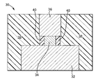
- FIG. 4 illustrates a cross-sectional view through a phase-change memory cell with a laterally surrounding isolation material in accordance with one embodiment of the present invention.
- FIG. 5 illustrates a cross-sectional view through a phase-change memory cell with a laterally surrounding isolation material in accordance with another embodiment of the present invention.
- FIG. 6 illustrates a graph plotting the cell resistance as obtained during a read operation as a function of the reset pulse voltage and current.
- FIG. 1 illustrates a block diagram of a memory cell device 5 .
- Memory cell device 5 includes write pulse generator 6 , distribution circuit 7 , and memory cells 8 a , 8 b , 8 c , and 8 d and a sense amplifier 9 .
- memory cells 8 a - 8 d are phase-change memory cells that are based on the amorphous to crystalline phase transition of the memory material.
- write pulse generator 6 generates current or voltage pulses that are controllable directed to memory cells 8 a - 8 d via distribution circuit 7 .
- distribution circuit 7 is a plurality of transistors that controllable direct current or voltage pulses to the memory, and in another embodiment, is a plurality of transistors that controllable direct current or voltage pulses to heaters adjacent to the phase-change memory cells.
- memory cells 8 a - 8 d are made of a phase-change material that may be changed from an amorphous state to a crystalline state or crystalline state to amorphous under influence of temperature change.
- the degree of crystallinity thereby defines at least two memory states for storing data within memory cell device 5 , which can be assigned to the bit values “0” and “1”.
- the bit states of memory cells 8 a - 8 d differ significantly in their electrical resistivity. In the amorphous state, a phase-change material will exhibit significantly higher resistivity than it will in the crystalline state. In this way, sense amplifier 9 may read the cell resistance such that the bit value assigned to a particular memory cell 8 a - 8 d can be determined.
- write pulse generator 6 In order to program a memory cell 8 a - 8 d within memory cell device 5 , write pulse generator 6 generates a current or voltage pulse for heating the phase-change material in the target memory cell. In one embodiment, write pulse generator 6 generates an appropriate current or voltage pulse, which is fed into distribution circuit 7 and distributed to the appropriate target memory cell 8 a - 8 d . The current or voltage pulse amplitude and duration is controlled depending on whether the memory cell is being set or reset. Generally, a “set” operation of a memory cell is heating the phase-change material of the target memory cell above its crystallization temperature (but below its melting temperature) long enough to achieve the crystalline state. Generally, a “reset” operation of a memory cell is quickly heating the phase-change material of the target memory cell above its melting temperature, and then quickly quench cooling the material, thereby achieving the amorphous state.
- FIG. 2 illustrates a cross-section view through an exemplary phase-change memory cell 10 of the active-in-via type.
- Phase-change memory cell 10 includes first electrode 12 , phase-change material 14 , second electrode 16 , and insulator material 18 .
- the phase change material 14 is laterally completely enclosed by insulation material 18 , which defines the current path and hence the location of the phase change region in phase change material 14 .
- a selection device such as an active device like a transistor or diode, may be coupled to first electrode 12 to control the application of current or voltage to first electrode 12 , and thus to phase-change material 14 , in order to set and reset phase-change material 14 .
- phase-change material 14 a set current or voltage pulse is selectively enabled to phase-change material 14 thereby heating it above its crystallization temperature (but below its melting temperature). In this way, phase-change material 14 reaches its crystalline state during this set operation.
- a reset current and/or voltage pulse is selectively enabled by the selection device and sent through first electrode 12 to phase-change material 14 . The reset current or voltage quickly heats phase-change material 14 above its melting temperature, and then phase-change material 14 is quickly quench cooled to achieve its amorphous state.
- phase-change material 14 typically begins heating and changing phases (melting) from the center of the cell due to thermal self-isolation of the phase-change material 14 . Generated heat, however, may also diffuse into insulator material 18 , which is typically an insulator material like silicon dioxide. Thus, in a low power reset operation, which avoids excessive overheating of the center, there is a crystalline, ring-shaped volume at the edge of phase-change material 14 remaining in the crystalline state due to incomplete melting. Such an incomplete melted area 22 is illustrated in FIG. 3 , surrounding a sufficiently melted area 20 in phase-change material 14 . A read operation undertaken subsequent to a reset in such a configuration provides low resistance shunt current paths in the area 22 . This will mask the readout signal detected by sense amplifier 9 in the high resistance state.
- FIG. 4 illustrates a cross-section view through an exemplary phase-change memory cell 30 in accordance with one embodiment of the present invention.
- Phase-change memory cell 30 includes first electrode 32 , phase-change material 34 , second electrode 36 , and insulator material 38 .
- phase-change memory cell 30 includes isolation material 40 adjacent phase-change material 34 .
- isolation material 40 is selected to have low thermal conductivity/diffusivity, thereby reducing the heat leakage from the edges of phase-change material 34 .
- phase-change memory cell 30 in an active-in-via (AIV) cell such that a reset pulse typically melts phase-change material 34 starting at its center, and then the melting front moves outward.
- isolation material 40 surrounds phase-change material 34 at its outer edges. This reduces heat leakage from the edge of phase-change material 34 by the improved thermal insulation provided by the surrounding isolation material 40 . In this way, unlike with phase-change memory device 10 , melting of phase-change material 34 during a low power reset operation tends to go all the way out to its edge, thereby avoiding the crystalline, ring-shaped volume found in the prior embodiment.
- phase-change material 34 Since even the outermost portions phase-change material 34 are melted (and subsequently amorphized during quench cooling), the total cell resistance will be much higher and read operation undertaken subsequent to a reset provides large read signals detected by sense amplifier 9 . In this way, less input power is needed to achieve adequate read margins during reset operations. This allows lowering the reset pulse signal compared to a cell without isolation material 40 , while still maintaining a switching of the full cell cross-section resulting in large read signals. Since the footprint of a scaled phase change memory cell is predominately determined by the width (and hence, area) of the select device required to drive the current during reset operation, this power reduction immediately translates into a more compact cell size.
- Phase-change memory cell 30 may be fabricated in several ways in accordance with the present invention. For example, phase-change material 34 may be deposited and then etched, and then isolation material 40 formed adjacent to the edges of phase-change material 34 . In addition, a layer of isolation material 40 may first be deposited, and then a via etched within the layer of isolation material 40 . Phase-change material 34 may then be deposited in the via within the layer of isolation material 40 .
- FIG. 5 illustrates a cross-section view through an exemplary phase-change memory cell 30 in accordance with another embodiment of the present invention.
- Phase-change memory cell 30 includes first electrode 32 , phase-change material 34 , second electrode 36 , and insulator material 38 .
- phase-change memory cell 30 includes isolation material 40 adjacent phase-change material 34 .
- isolation material 40 is only placed immediately adjacent phase-change material 34 , and is also selected to have low thermal conductivity.
- less isolation material 40 is used, but heat leakage from the edges of phase-change material 34 is nonetheless effectively reduced. In this way, less additional input power is needed to achieve the increase in temperature that is needed for sufficient reset operations.
- FIG. 6 displays a graph plotting the cell resistance as obtained during a read operation as a function of the reset pulse voltage and current for three exemplary phase-change memory cells.
- the onset of melting at the center of the phase change cell is illustrated by a dotted vertical line.
- Line 70 in FIG. 6 illustrates the characteristics of a phase-change memory cell where the phase-change material is surrounded by silicon dioxide as insulating material.
- the cell does not display a sharp switching characteristic, but instead displays a long lag phase having relatively low read resistance. This is due to the partial melting of the phase change material in the cell discussed earlier, which results in the highly conductive connection at the outer edge of the phase change material.
- Line 60 in FIG. 6 illustrates the characteristics of a phase-change memory cell where the phase-change material is surrounded by a thermal insulating material having a relatively low dielectric constant (“low-k”), such as a porous oxide.
- low-k dielectric constant
- the read resistivity displays an improved switching characteristic over line 70 , and displays shorter lag phase having relatively higher read resistance.
- Line 50 in FIG. 6 illustrates the characteristics of a phase-change memory cell where the phase-change material is surrounded by a thermal insulating material having a relatively low-k, such as Aerogel.
- the read resistance displays an improved and sharp switching characteristic over line 60 , and the lag phase of line 70 virtually vanishes.
- the read resistance illustrates a sharp transition over several orders of magnitude.
- isolation material 40 is a good thermal insulator dielectric material such as a porous oxide film having a thermal conductivity between 0.1 and 0.8 W/(mK).
- isolation material 40 may be a dielectric material such as Aerogel material with a thermal conductivity of about 0.12-0.18 W/mK, and in another it may be a templated porous oxide dielectric such as Philk with a thermal conductivity of about 0.13-0.17 W/mK.
- Phase-change material 34 may be made up of a variety of materials in accordance with the present invention. Generally, chalcogenide alloys that contain one or more elements from Column IV of the periodic table are useful as such materials.
- phase-change material 34 of memory cell 30 is made up of a chalcogenide compound material, such as GeSbTe or AgInSbTe.
- the phase change material can be chalcogen-free such as GeSb, GaSb or GeGaSb.
- low-k dielectric materials function as isolation material 40 for these types of phase-change materials 34
- other low-k dielectrics may also be usable for different types of phase-change materials that may be operated at relatively higher temperatures.
- Such low-k dielectric materials include SiLK, Coral, LDK-5109, Orion® 2.2, CF-Polymer, and others.
- phase-change memory cell Use of a low-k dielectric material surrounding the phase-change material in a phase-change memory cell allows a lowering of the reset pulse power (current and/or voltage) compared to a phase-change cell without low-k dielectric material surrounding the phase-change material, while still maintaining a switching of the full cell cross-section resulting in large read signals. This allows for reduced phase-change memory cell size and thus chip size as well, allowing for increased chip density.
Abstract
Description
Claims (26)
Priority Applications (14)
| Application Number | Priority Date | Filing Date | Title |
|---|---|---|---|
| US11/054,853 US7361925B2 (en) | 2005-02-10 | 2005-02-10 | Integrated circuit having a memory including a low-k dielectric material for thermal isolation |
| US11/102,350 US7348590B2 (en) | 2005-02-10 | 2005-04-08 | Phase change memory cell with high read margin at low power operation |
| US11/101,972 US7214958B2 (en) | 2005-02-10 | 2005-04-08 | Phase change memory cell with high read margin at low power operation |
| KR1020067014085A KR100873973B1 (en) | 2005-02-10 | 2006-02-08 | Phase Change Memory Cell with High Read Margin with Low Power Operation |
| KR1020077020518A KR20070103480A (en) | 2005-02-10 | 2006-02-08 | Phase change memory cell with high read margin at low power operation |
| PCT/EP2006/050751 WO2006084857A1 (en) | 2005-02-10 | 2006-02-08 | Phase change memory cell with high read margin at low power operation |
| PCT/EP2006/050750 WO2006084856A1 (en) | 2005-02-10 | 2006-02-08 | Phase change memory cell with high read margin at low power operation |
| JP2007554550A JP2008530790A (en) | 2005-02-10 | 2006-02-08 | Phase change memory cell with high read margin in low power operation |
| EP06708097A EP1846961A1 (en) | 2005-02-10 | 2006-02-08 | Phase change memory cell with high read margin at low power operation |
| CNA2006800043049A CN101116195A (en) | 2005-02-10 | 2006-02-08 | Phase change memory cell with high read margin at low power operation |
| EP06708098A EP1846962B1 (en) | 2005-02-10 | 2006-02-08 | Phase change memory cell with high read margin at low power operation |
| US11/737,838 US7714312B2 (en) | 2005-02-10 | 2007-04-20 | Phase change memory cell with high read margin at low power operation |
| US11/737,847 US7674709B2 (en) | 2005-02-10 | 2007-04-20 | Phase change memory cell with high read margin at low power operation |
| US12/050,727 US7824951B2 (en) | 2005-02-10 | 2008-03-18 | Method of fabricating an integrated circuit having a memory including a low-k dielectric material |
Applications Claiming Priority (1)
| Application Number | Priority Date | Filing Date | Title |
|---|---|---|---|
| US11/054,853 US7361925B2 (en) | 2005-02-10 | 2005-02-10 | Integrated circuit having a memory including a low-k dielectric material for thermal isolation |
Related Child Applications (5)
| Application Number | Title | Priority Date | Filing Date |
|---|---|---|---|
| US11/101,972 Continuation-In-Part US7214958B2 (en) | 2005-02-10 | 2005-04-08 | Phase change memory cell with high read margin at low power operation |
| US11/102,350 Continuation-In-Part US7348590B2 (en) | 2005-02-10 | 2005-04-08 | Phase change memory cell with high read margin at low power operation |
| US11/737,847 Continuation-In-Part US7674709B2 (en) | 2005-02-10 | 2007-04-20 | Phase change memory cell with high read margin at low power operation |
| US11/737,838 Continuation-In-Part US7714312B2 (en) | 2005-02-10 | 2007-04-20 | Phase change memory cell with high read margin at low power operation |
| US12/050,727 Division US7824951B2 (en) | 2005-02-10 | 2008-03-18 | Method of fabricating an integrated circuit having a memory including a low-k dielectric material |
Publications (2)
| Publication Number | Publication Date |
|---|---|
| US20060175596A1 US20060175596A1 (en) | 2006-08-10 |
| US7361925B2 true US7361925B2 (en) | 2008-04-22 |
Family
ID=36779066
Family Applications (2)
| Application Number | Title | Priority Date | Filing Date |
|---|---|---|---|
| US11/054,853 Expired - Fee Related US7361925B2 (en) | 2005-02-10 | 2005-02-10 | Integrated circuit having a memory including a low-k dielectric material for thermal isolation |
| US12/050,727 Expired - Fee Related US7824951B2 (en) | 2005-02-10 | 2008-03-18 | Method of fabricating an integrated circuit having a memory including a low-k dielectric material |
Family Applications After (1)
| Application Number | Title | Priority Date | Filing Date |
|---|---|---|---|
| US12/050,727 Expired - Fee Related US7824951B2 (en) | 2005-02-10 | 2008-03-18 | Method of fabricating an integrated circuit having a memory including a low-k dielectric material |
Country Status (2)
| Country | Link |
|---|---|
| US (2) | US7361925B2 (en) |
| CN (1) | CN101116195A (en) |
Cited By (3)
| Publication number | Priority date | Publication date | Assignee | Title |
|---|---|---|---|---|
| US20100270527A1 (en) * | 2009-04-27 | 2010-10-28 | Kabushiki Kaisha Toshiba | Phase-change memory device and method of manufacturing the phase-change memory device |
| USRE45356E1 (en) * | 2005-09-07 | 2015-02-03 | Electronics And Telecommunications Research Institute | Phase-change memory device using Sb-Se metal alloy and method of fabricating the same |
| US9780302B2 (en) | 2013-11-22 | 2017-10-03 | Taiwan Semiconductor Manufacturing Co., Ltd. | Top electrode for device structures in interconnect |
Families Citing this family (36)
| Publication number | Priority date | Publication date | Assignee | Title |
|---|---|---|---|---|
| US8237140B2 (en) | 2005-06-17 | 2012-08-07 | Macronix International Co., Ltd. | Self-aligned, embedded phase change RAM |
| US7417245B2 (en) * | 2005-11-02 | 2008-08-26 | Infineon Technologies Ag | Phase change memory having multilayer thermal insulation |
| US8017930B2 (en) * | 2006-12-21 | 2011-09-13 | Qimonda Ag | Pillar phase change memory cell |
| US20080278988A1 (en) * | 2007-05-09 | 2008-11-13 | Klaus Ufert | Resistive switching element |
| US7642125B2 (en) | 2007-09-14 | 2010-01-05 | Macronix International Co., Ltd. | Phase change memory cell in via array with self-aligned, self-converged bottom electrode and method for manufacturing |
| US8178386B2 (en) | 2007-09-14 | 2012-05-15 | Macronix International Co., Ltd. | Phase change memory cell array with self-converged bottom electrode and method for manufacturing |
| CN101335327B (en) * | 2008-08-05 | 2010-06-16 | 中国科学院上海微系统与信息技术研究所 | Method for controlling phase-change material or phase-change memory unit volume change and corresponding construction |
| US8829646B2 (en) * | 2009-04-27 | 2014-09-09 | Macronix International Co., Ltd. | Integrated circuit 3D memory array and manufacturing method |
| US8551855B2 (en) * | 2009-10-23 | 2013-10-08 | Sandisk 3D Llc | Memory cell that includes a carbon-based reversible resistance switching element compatible with a steering element, and methods of forming the same |
| US8481396B2 (en) * | 2009-10-23 | 2013-07-09 | Sandisk 3D Llc | Memory cell that includes a carbon-based reversible resistance switching element compatible with a steering element, and methods of forming the same |
| US8551850B2 (en) * | 2009-12-07 | 2013-10-08 | Sandisk 3D Llc | Methods of forming a reversible resistance-switching metal-insulator-metal structure |
| US8847195B2 (en) * | 2009-12-24 | 2014-09-30 | Micron Technology, Inc. | Structures for resistance random access memory and methods of forming the same |
| US8389375B2 (en) * | 2010-02-11 | 2013-03-05 | Sandisk 3D Llc | Memory cell formed using a recess and methods for forming the same |
| US8237146B2 (en) * | 2010-02-24 | 2012-08-07 | Sandisk 3D Llc | Memory cell with silicon-containing carbon switching layer and methods for forming the same |
| US20110210306A1 (en) * | 2010-02-26 | 2011-09-01 | Yubao Li | Memory cell that includes a carbon-based memory element and methods of forming the same |
| US8471360B2 (en) | 2010-04-14 | 2013-06-25 | Sandisk 3D Llc | Memory cell with carbon switching material having a reduced cross-sectional area and methods for forming the same |
| US8097537B2 (en) | 2010-05-25 | 2012-01-17 | Micron Technology, Inc. | Phase change memory cell structures and methods |
| US9082954B2 (en) | 2010-09-24 | 2015-07-14 | Macronix International Co., Ltd. | PCRAM with current flowing laterally relative to axis defined by electrodes |
| CN102005466A (en) * | 2010-09-28 | 2011-04-06 | 中国科学院上海微系统与信息技术研究所 | Phase change memory structure with low-k medium heat insulating material and preparation method |
| US8735863B2 (en) * | 2011-01-28 | 2014-05-27 | Privatran | Integrated nonvolatile resistive memory elements |
| US8497182B2 (en) | 2011-04-19 | 2013-07-30 | Macronix International Co., Ltd. | Sidewall thin film electrode with self-aligned top electrode and programmable resistance memory |
| US8987700B2 (en) | 2011-12-02 | 2015-03-24 | Macronix International Co., Ltd. | Thermally confined electrode for programmable resistance memory |
| US8981330B2 (en) | 2012-07-16 | 2015-03-17 | Macronix International Co., Ltd. | Thermally-confined spacer PCM cells |
| CN103840077B (en) * | 2012-11-27 | 2016-04-20 | 中芯国际集成电路制造(上海)有限公司 | The manufacture method of phase transition storage |
| US9214351B2 (en) | 2013-03-12 | 2015-12-15 | Macronix International Co., Ltd. | Memory architecture of thin film 3D array |
| US8916414B2 (en) | 2013-03-13 | 2014-12-23 | Macronix International Co., Ltd. | Method for making memory cell by melting phase change material in confined space |
| US9136473B2 (en) * | 2013-03-28 | 2015-09-15 | Stmicroelectronics, Inc. | Semiconductor device with PCM memory cells and nanotubes and related methods |
| CN103594621B (en) * | 2013-11-05 | 2016-03-09 | 中国科学院苏州纳米技术与纳米仿生研究所 | A kind of phase-change memory cell and preparation method thereof |
| US9336879B2 (en) | 2014-01-24 | 2016-05-10 | Macronix International Co., Ltd. | Multiple phase change materials in an integrated circuit for system on a chip application |
| US9559113B2 (en) | 2014-05-01 | 2017-01-31 | Macronix International Co., Ltd. | SSL/GSL gate oxide in 3D vertical channel NAND |
| CN106206639B (en) * | 2015-05-25 | 2019-08-06 | 江苏时代全芯存储科技股份有限公司 | Phase change memory storage and its manufacturing method with needle-shaped junction |
| CN105609632B (en) * | 2015-12-24 | 2019-03-05 | 江苏时代全芯存储科技有限公司 | Phase-change memory and its manufacturing method |
| US9793323B1 (en) | 2016-07-11 | 2017-10-17 | Macronix International Co., Ltd. | Phase change memory with high endurance |
| CN109786550B (en) * | 2019-03-18 | 2024-04-05 | 北京时代全芯存储技术股份有限公司 | Phase change memory and method for manufacturing the same |
| US11812676B2 (en) | 2020-03-24 | 2023-11-07 | International Business Machines Corporation | Multi-terminal phase change memory device |
| US20230093026A1 (en) * | 2021-09-20 | 2023-03-23 | International Business Machines Corporation | Insulated phase change memory using porous dielectrics |
Citations (18)
| Publication number | Priority date | Publication date | Assignee | Title |
|---|---|---|---|---|
| US5751012A (en) | 1995-06-07 | 1998-05-12 | Micron Technology, Inc. | Polysilicon pillar diode for use in a non-volatile memory cell |
| US5837564A (en) | 1995-11-01 | 1998-11-17 | Micron Technology, Inc. | Method for optimal crystallization to obtain high electrical performance from chalcogenides |
| US6339544B1 (en) * | 2000-09-29 | 2002-01-15 | Intel Corporation | Method to enhance performance of thermal resistor device |
| US20020017701A1 (en) | 1999-03-25 | 2002-02-14 | Patrick Klersy | Electrically programmable memory element with raised pore |
| US20030003647A1 (en) | 2001-06-30 | 2003-01-02 | Dennison Charles H. | Reduced area intersection between electrode and programming element |
| US6507061B1 (en) * | 2001-08-31 | 2003-01-14 | Intel Corporation | Multiple layer phase-change memory |
| EP1318552A1 (en) | 2001-12-05 | 2003-06-11 | STMicroelectronics S.r.l. | Small area contact region, high efficiency phase change memory cell and fabrication method thereof |
| US6625054B2 (en) | 2001-12-28 | 2003-09-23 | Intel Corporation | Method and apparatus to program a phase change memory |
| US20030194865A1 (en) | 2002-04-10 | 2003-10-16 | Gilton Terry L. | Method of manufacture of programmable conductor memory |
| US6673648B2 (en) | 2001-11-08 | 2004-01-06 | Intel Corporation | Isolating phase change material memory cells |
| DE10236439B3 (en) | 2002-08-08 | 2004-02-26 | Infineon Technologies Ag | Memory arrangement comprises a substrate, memory regions formed in and/or on the substrate with electrical resistances that can be adjusted by thermal treatment and structure arranged between the memory regions to remove heat |
| US20040051094A1 (en) * | 2002-09-13 | 2004-03-18 | Mitsubishi Denki Kabushiki Kaisha | Non-volatile semiconductor memory device allowing shrinking of memory cell |
| DE10231646A1 (en) | 2002-07-12 | 2004-04-08 | Infineon Technologies Ag | Memory cell for permanently storing data has a switching unit with a field effect transistor having a drain region formed as the heating region |
| US6791102B2 (en) * | 2002-12-13 | 2004-09-14 | Intel Corporation | Phase change memory |
| US20040251551A1 (en) | 2003-06-11 | 2004-12-16 | Horii Hideki | Phase changeable memory devices including carbon nano tubes and methods for forming the same |
| US6937507B2 (en) * | 2003-12-05 | 2005-08-30 | Silicon Storage Technology, Inc. | Memory device and method of operating same |
| US20060092693A1 (en) * | 2004-11-01 | 2006-05-04 | Bomy Chen | Phase change memory device employing thermally insulating voids and sloped trench, and a method of making same |
| US20060163554A1 (en) * | 2002-10-11 | 2006-07-27 | Koninklijke Philips Electronics N.C. | Electric device comprising phase change material |
Family Cites Families (4)
| Publication number | Priority date | Publication date | Assignee | Title |
|---|---|---|---|---|
| US6531373B2 (en) * | 2000-12-27 | 2003-03-11 | Ovonyx, Inc. | Method of forming a phase-change memory cell using silicon on insulator low electrode in charcogenide elements |
| US7102150B2 (en) * | 2001-05-11 | 2006-09-05 | Harshfield Steven T | PCRAM memory cell and method of making same |
| US6891749B2 (en) * | 2002-02-20 | 2005-05-10 | Micron Technology, Inc. | Resistance variable ‘on ’ memory |
| US7018918B2 (en) * | 2002-11-21 | 2006-03-28 | Intel Corporation | Method of forming a selectively converted inter-layer dielectric using a porogen material |
-
2005
- 2005-02-10 US US11/054,853 patent/US7361925B2/en not_active Expired - Fee Related
-
2006
- 2006-02-08 CN CNA2006800043049A patent/CN101116195A/en active Pending
-
2008
- 2008-03-18 US US12/050,727 patent/US7824951B2/en not_active Expired - Fee Related
Patent Citations (18)
| Publication number | Priority date | Publication date | Assignee | Title |
|---|---|---|---|---|
| US5751012A (en) | 1995-06-07 | 1998-05-12 | Micron Technology, Inc. | Polysilicon pillar diode for use in a non-volatile memory cell |
| US5837564A (en) | 1995-11-01 | 1998-11-17 | Micron Technology, Inc. | Method for optimal crystallization to obtain high electrical performance from chalcogenides |
| US20020017701A1 (en) | 1999-03-25 | 2002-02-14 | Patrick Klersy | Electrically programmable memory element with raised pore |
| US6339544B1 (en) * | 2000-09-29 | 2002-01-15 | Intel Corporation | Method to enhance performance of thermal resistor device |
| US20030003647A1 (en) | 2001-06-30 | 2003-01-02 | Dennison Charles H. | Reduced area intersection between electrode and programming element |
| US6507061B1 (en) * | 2001-08-31 | 2003-01-14 | Intel Corporation | Multiple layer phase-change memory |
| US6673648B2 (en) | 2001-11-08 | 2004-01-06 | Intel Corporation | Isolating phase change material memory cells |
| EP1318552A1 (en) | 2001-12-05 | 2003-06-11 | STMicroelectronics S.r.l. | Small area contact region, high efficiency phase change memory cell and fabrication method thereof |
| US6625054B2 (en) | 2001-12-28 | 2003-09-23 | Intel Corporation | Method and apparatus to program a phase change memory |
| US20030194865A1 (en) | 2002-04-10 | 2003-10-16 | Gilton Terry L. | Method of manufacture of programmable conductor memory |
| DE10231646A1 (en) | 2002-07-12 | 2004-04-08 | Infineon Technologies Ag | Memory cell for permanently storing data has a switching unit with a field effect transistor having a drain region formed as the heating region |
| DE10236439B3 (en) | 2002-08-08 | 2004-02-26 | Infineon Technologies Ag | Memory arrangement comprises a substrate, memory regions formed in and/or on the substrate with electrical resistances that can be adjusted by thermal treatment and structure arranged between the memory regions to remove heat |
| US20040051094A1 (en) * | 2002-09-13 | 2004-03-18 | Mitsubishi Denki Kabushiki Kaisha | Non-volatile semiconductor memory device allowing shrinking of memory cell |
| US20060163554A1 (en) * | 2002-10-11 | 2006-07-27 | Koninklijke Philips Electronics N.C. | Electric device comprising phase change material |
| US6791102B2 (en) * | 2002-12-13 | 2004-09-14 | Intel Corporation | Phase change memory |
| US20040251551A1 (en) | 2003-06-11 | 2004-12-16 | Horii Hideki | Phase changeable memory devices including carbon nano tubes and methods for forming the same |
| US6937507B2 (en) * | 2003-12-05 | 2005-08-30 | Silicon Storage Technology, Inc. | Memory device and method of operating same |
| US20060092693A1 (en) * | 2004-11-01 | 2006-05-04 | Bomy Chen | Phase change memory device employing thermally insulating voids and sloped trench, and a method of making same |
Non-Patent Citations (2)
| Title |
|---|
| Ha, Y. H. et al., "An Edge Contact Type Cell for Phase Change RAM Featuring Very Low Power Consumption," Symposium on VLSI Technology Digest of Technical Papers, pp. 2, (2003). |
| Horii, H. et al., "A Novel Cell Technology Using N-Doped GeSbTe Films for Phase Change RAM," symposium on VLSI Technology Digest of Technical Papers, pp. 2, (2003). |
Cited By (6)
| Publication number | Priority date | Publication date | Assignee | Title |
|---|---|---|---|---|
| USRE45356E1 (en) * | 2005-09-07 | 2015-02-03 | Electronics And Telecommunications Research Institute | Phase-change memory device using Sb-Se metal alloy and method of fabricating the same |
| US20100270527A1 (en) * | 2009-04-27 | 2010-10-28 | Kabushiki Kaisha Toshiba | Phase-change memory device and method of manufacturing the phase-change memory device |
| US9780302B2 (en) | 2013-11-22 | 2017-10-03 | Taiwan Semiconductor Manufacturing Co., Ltd. | Top electrode for device structures in interconnect |
| US10276790B2 (en) | 2013-11-22 | 2019-04-30 | Taiwan Semiconductor Manufacturing Co., Ltd. | Top electrode for device structures in interconnect |
| US10510953B2 (en) | 2013-11-22 | 2019-12-17 | Taiwan Semiconductor Manufacturing Co., Ltd. | Top electrode for device structures in interconnect |
| US10862029B2 (en) | 2013-11-22 | 2020-12-08 | Taiwan Semiconductor Manufacturing Co., Ltd. | Top electrode for device structures in interconnect |
Also Published As
| Publication number | Publication date |
|---|---|
| US20080158943A1 (en) | 2008-07-03 |
| CN101116195A (en) | 2008-01-30 |
| US20060175596A1 (en) | 2006-08-10 |
| US7824951B2 (en) | 2010-11-02 |
Similar Documents
| Publication | Publication Date | Title |
|---|---|---|
| US7361925B2 (en) | Integrated circuit having a memory including a low-k dielectric material for thermal isolation | |
| US7348590B2 (en) | Phase change memory cell with high read margin at low power operation | |
| US7214958B2 (en) | Phase change memory cell with high read margin at low power operation | |
| US7973384B2 (en) | Phase change memory cell including multiple phase change material portions | |
| US7615770B2 (en) | Integrated circuit having an insulated memory | |
| EP1870903B1 (en) | Memory cell programmed using a temperature controlled set pulse | |
| US9123415B2 (en) | Methods of operating a phase change memory cell | |
| US7973301B2 (en) | Low power phase change memory cell with large read signal | |
| TW200919716A (en) | Programmable fuse/non-volatile memory structures in BEOL regions using externally heated phase change material | |
| US20070267620A1 (en) | Memory cell including doped phase change material | |
| US7031181B1 (en) | Multi-pulse reset write scheme for phase-change memories | |
| US8189374B2 (en) | Memory device including an electrode having an outer portion with greater resistivity | |
| EP4187540A1 (en) | Phase change memory device with improved retention characteristics and related method |
Legal Events
| Date | Code | Title | Description |
|---|---|---|---|
| AS | Assignment |
Owner name: INFINEON TECHNOLOGIES NORTH AMERICA CORP., CALIFOR Free format text: ASSIGNMENT OF ASSIGNORS INTEREST;ASSIGNORS:HAPP, THOMAS;ZAIDI, SHOAIB;REEL/FRAME:015890/0068 Effective date: 20050210 |
|
| AS | Assignment |
Owner name: INFINEON TECHNOLOGIES AG, GERMANY Free format text: ASSIGNMENT OF ASSIGNORS INTEREST;ASSIGNOR:INFINEON TECHNOLOGIES NORTH AMERICA CORP.;REEL/FRAME:015970/0990 Effective date: 20050503 |
|
| FEPP | Fee payment procedure |
Free format text: PAYOR NUMBER ASSIGNED (ORIGINAL EVENT CODE: ASPN); ENTITY STATUS OF PATENT OWNER: LARGE ENTITY |
|
| STCF | Information on status: patent grant |
Free format text: PATENTED CASE |
|
| AS | Assignment |
Owner name: QIMONDA AG, GERMANY Free format text: ASSIGNMENT OF ASSIGNORS INTEREST;ASSIGNOR:INFINEON TECHNOLOGIES AG;REEL/FRAME:023806/0001 Effective date: 20060425 Owner name: QIMONDA AG,GERMANY Free format text: ASSIGNMENT OF ASSIGNORS INTEREST;ASSIGNOR:INFINEON TECHNOLOGIES AG;REEL/FRAME:023806/0001 Effective date: 20060425 |
|
| FPAY | Fee payment |
Year of fee payment: 4 |
|
| CC | Certificate of correction | ||
| CC | Certificate of correction | ||
| AS | Assignment |
Owner name: INFINEON TECHNOLOGIES AG, GERMANY Free format text: ASSIGNMENT OF ASSIGNORS INTEREST;ASSIGNOR:QIMONDA AG;REEL/FRAME:035623/0001 Effective date: 20141009 |
|
| AS | Assignment |
Owner name: POLARIS INNOVATIONS LIMITED, IRELAND Free format text: ASSIGNMENT OF ASSIGNORS INTEREST;ASSIGNOR:INFINEON TECHNOLOGIES AG;REEL/FRAME:036908/0923 Effective date: 20150708 |
|
| REMI | Maintenance fee reminder mailed | ||
| FPAY | Fee payment |
Year of fee payment: 8 |
|
| SULP | Surcharge for late payment |
Year of fee payment: 7 |
|
| FEPP | Fee payment procedure |
Free format text: MAINTENANCE FEE REMINDER MAILED (ORIGINAL EVENT CODE: REM.); ENTITY STATUS OF PATENT OWNER: LARGE ENTITY |
|
| LAPS | Lapse for failure to pay maintenance fees |
Free format text: PATENT EXPIRED FOR FAILURE TO PAY MAINTENANCE FEES (ORIGINAL EVENT CODE: EXP.); ENTITY STATUS OF PATENT OWNER: LARGE ENTITY |
|
| STCH | Information on status: patent discontinuation |
Free format text: PATENT EXPIRED DUE TO NONPAYMENT OF MAINTENANCE FEES UNDER 37 CFR 1.362 |
|
| FP | Lapsed due to failure to pay maintenance fee |
Effective date: 20200422 |