US7372406B2 - Antenna apparatus including inverted-F antenna having variable resonance frequency - Google Patents
Antenna apparatus including inverted-F antenna having variable resonance frequency Download PDFInfo
- Publication number
- US7372406B2 US7372406B2 US10/639,490 US63949003A US7372406B2 US 7372406 B2 US7372406 B2 US 7372406B2 US 63949003 A US63949003 A US 63949003A US 7372406 B2 US7372406 B2 US 7372406B2
- Authority
- US
- United States
- Prior art keywords
- antenna
- resonance frequency
- terminal
- switch
- inverted
- Prior art date
- Legal status (The legal status is an assumption and is not a legal conclusion. Google has not performed a legal analysis and makes no representation as to the accuracy of the status listed.)
- Expired - Fee Related, expires
Links
Images


Classifications
-
- H—ELECTRICITY
- H01—ELECTRIC ELEMENTS
- H01Q—ANTENNAS, i.e. RADIO AERIALS
- H01Q1/00—Details of, or arrangements associated with, antennas
- H01Q1/12—Supports; Mounting means
- H01Q1/22—Supports; Mounting means by structural association with other equipment or articles
- H01Q1/2258—Supports; Mounting means by structural association with other equipment or articles used with computer equipment
- H01Q1/2266—Supports; Mounting means by structural association with other equipment or articles used with computer equipment disposed inside the computer
-
- G—PHYSICS
- G06—COMPUTING; CALCULATING OR COUNTING
- G06F—ELECTRIC DIGITAL DATA PROCESSING
- G06F1/00—Details not covered by groups G06F3/00 - G06F13/00 and G06F21/00
- G06F1/16—Constructional details or arrangements
- G06F1/1613—Constructional details or arrangements for portable computers
- G06F1/1615—Constructional details or arrangements for portable computers with several enclosures having relative motions, each enclosure supporting at least one I/O or computing function
- G06F1/1616—Constructional details or arrangements for portable computers with several enclosures having relative motions, each enclosure supporting at least one I/O or computing function with folding flat displays, e.g. laptop computers or notebooks having a clamshell configuration, with body parts pivoting to an open position around an axis parallel to the plane they define in closed position
-
- G—PHYSICS
- G06—COMPUTING; CALCULATING OR COUNTING
- G06F—ELECTRIC DIGITAL DATA PROCESSING
- G06F1/00—Details not covered by groups G06F3/00 - G06F13/00 and G06F21/00
- G06F1/16—Constructional details or arrangements
- G06F1/1613—Constructional details or arrangements for portable computers
- G06F1/1633—Constructional details or arrangements of portable computers not specific to the type of enclosures covered by groups G06F1/1615 - G06F1/1626
- G06F1/1684—Constructional details or arrangements related to integrated I/O peripherals not covered by groups G06F1/1635 - G06F1/1675
- G06F1/1698—Constructional details or arrangements related to integrated I/O peripherals not covered by groups G06F1/1635 - G06F1/1675 the I/O peripheral being a sending/receiving arrangement to establish a cordless communication link, e.g. radio or infrared link, integrated cellular phone
-
- H—ELECTRICITY
- H01—ELECTRIC ELEMENTS
- H01Q—ANTENNAS, i.e. RADIO AERIALS
- H01Q3/00—Arrangements for changing or varying the orientation or the shape of the directional pattern of the waves radiated from an antenna or antenna system
- H01Q3/24—Arrangements for changing or varying the orientation or the shape of the directional pattern of the waves radiated from an antenna or antenna system varying the orientation by switching energy from one active radiating element to another, e.g. for beam switching
-
- H—ELECTRICITY
- H01—ELECTRIC ELEMENTS
- H01Q—ANTENNAS, i.e. RADIO AERIALS
- H01Q9/00—Electrically-short antennas having dimensions not more than twice the operating wavelength and consisting of conductive active radiating elements
- H01Q9/04—Resonant antennas
- H01Q9/06—Details
- H01Q9/14—Length of element or elements adjustable
- H01Q9/145—Length of element or elements adjustable by varying the electrical length
-
- H—ELECTRICITY
- H01—ELECTRIC ELEMENTS
- H01Q—ANTENNAS, i.e. RADIO AERIALS
- H01Q9/00—Electrically-short antennas having dimensions not more than twice the operating wavelength and consisting of conductive active radiating elements
- H01Q9/04—Resonant antennas
- H01Q9/30—Resonant antennas with feed to end of elongated active element, e.g. unipole
- H01Q9/42—Resonant antennas with feed to end of elongated active element, e.g. unipole with folded element, the folded parts being spaced apart a small fraction of the operating wavelength
-
- H—ELECTRICITY
- H01—ELECTRIC ELEMENTS
- H01Q—ANTENNAS, i.e. RADIO AERIALS
- H01Q5/00—Arrangements for simultaneous operation of antennas on two or more different wavebands, e.g. dual-band or multi-band arrangements
- H01Q5/30—Arrangements for providing operation on different wavebands
- H01Q5/307—Individual or coupled radiating elements, each element being fed in an unspecified way
- H01Q5/314—Individual or coupled radiating elements, each element being fed in an unspecified way using frequency dependent circuits or components, e.g. trap circuits or capacitors
- H01Q5/321—Individual or coupled radiating elements, each element being fed in an unspecified way using frequency dependent circuits or components, e.g. trap circuits or capacitors within a radiating element or between connected radiating elements
Definitions
- the present invention relates to an antenna apparatus, and more particularly to an information processing apparatus having an inverted-F antenna.
- Some current desktop personal computers include respective television tuner cards.
- a tuner card is connected via a coaxial cable to an antenna for receiving terrestrial broadcast signals and an antenna dish for receiving satellite broadcast signals, both of which are mounted on a rooftop.
- mobile apparatuses such as notebook personal computers (PCs) and personal digital assistants (PDAs), having the capabilities of performing wireless communications via respective small size antennas coupled to the apparatuses, such as the wireless LAN communications, the Bluetooth standard short distance wireless communications and the mobile telephone communications, have been spreading widely.
- Such mobile apparatuses cannot receive the current terrestrial analog television signals in good condition with respective small antennas coupled to the apparatuses.
- most mobile apparatuses do not include television tuner cards.
- terrestrial digital television broadcasting becomes available in Japan, such mobile apparatuses will be able to receive, with respective small antennas, relatively high quality RF signals with carriers modulated with digital image signals.
- many mobile apparatuses will have a capability of receiving terrestrial digital television broadcast signals.
- RF signals of a plurality of terrestrial television broadcasts exhibit lower frequencies and a wider frequency range than those of the wireless LAN communications and other short distance wireless communications. Transmission and reception of RF signals of a plurality of terrestrial television broadcasts require a relatively large size antenna, which cannot be accommodated in a mobile apparatus.
- JP-A Japanese Patent Application Laid-Open Publication (JP-A) No. HEI 11-251825 discloses a small inverted-F antenna which can be accommodated in a small mobile communication apparatus.
- This inverted-F antenna has an antenna length equal to one quarter of the wavelength ⁇ of the transmitted and received RF signal, and is suitable for implementing in a mobile communication apparatus.
- the inverted-F antenna is associated with a resonant circuit for controlling radiator length in accordance with the frequency and also a resonant circuit for controlling the distance between the feed point and the ground in accordance with the frequency.
- variable capacitance diode is employed for a resonant circuit to control its resonance frequency.
- the typical range of tuning capacitance of such a variable capacitor is relatively small. Widening the range of variable capacitance requires an undesirable relatively high control voltage to be applied to the capacitor.
- JP-A Japanese Patent Application Laid-Open Publication (JP-A) No. HEI 10-284919 discloses a small antenna apparatus for a mobile communication unit for transmitting and receiving a wide range of RF signals.
- This antenna apparatus includes the antenna proper and a frequency tuning circuit.
- the tuning circuit includes an arrangement formed by a diode and a capacitor coupled in parallel. The resonance frequency of the antenna is varied by controlling the on/off operation of the diode.
- the inventors have recognized the need for an inverted-F antenna, which has a variable capacitor controllable with a relatively low control voltage, and which has a wider frequency range for receiving RF signals of a plurality of terrestrial broadcasts.
- An object of the present invention is to provide an inverted-F antenna that has a wider frequency range.
- Another object of the invention is to provide tuning of a resonance frequency of an inverted-F antenna with a wider frequency range.
- an antenna apparatus includes an inverted-F antenna having at least two antenna conductive elements coupled in series via at least one switch, and control means for controlling the at least one switch.
- an antenna apparatus includes an inverted-F antenna having at least two antenna conductive elements to be coupled in series via at least one resonant circuit.
- an information processing apparatus includes a plurality of such antenna apparatuses, and means for selecting one of the plurality of antenna apparatuses.
- an information processing apparatus includes a plurality of such antenna apparatuses.
- the plurality of antenna apparatuses are oriented in respective different directions.
- an information processing apparatus includes such an antenna apparatus, and channel changing means for controlling said antenna apparatus in accordance with receiving channel information provided by a user.
- an inverted-F antenna that has a wider frequency range can be provided.
- FIG. 1 shows a partially cutaway perspective view illustrating a mobile information processing apparatus, such as a notebook personal computer or a PDA, in accordance with an embodiment of the present invention
- FIG. 2 illustrates the configuration of an inverted-F antenna and its associated components, which can be used for the inverted-F antennas shown in FIG. 1 , in accordance with an embodiment of the invention
- FIG. 3 illustrates the configuration of an inverted-F antenna and its associated components which can be used for the inverted-F antennas shown in FIG. 1 , in accordance with another embodiment of the invention
- FIG. 4 shows a table representing the relationship of the resonance frequency of the inverted-F antenna relative to the positions of the switches in the switching and tuning units, and the values of the impedance of the LC resonant circuits containing the variable capacitors;
- FIG. 5 shows the tuning ranges of the resonance frequency and the VSWR in accordance with the embodiment of FIG. 3 ;
- FIG. 6 illustrates the configuration of an inverted-F antenna and its associated components which can be used for the inverted-F antennas shown in FIG. 1 , in accordance with a further embodiment of the invention
- FIG. 7 shows a table representing the relationship of the resonance frequency of the inverted-F antenna relative to the positions of the switches in the switching and tuning units, and the values of the impedance of the LC resonant circuits containing the variable capacitors;
- FIG. 8 illustrates the configuration of the inverted-F antennas shown in FIG. 1 and their associated components, in accordance with a still further embodiment of the invention
- FIG. 9 shows the relationship between the variable effective length and the resonance frequency for the inverted-F antennas shown in FIG. 8 ;
- FIG. 10 shows the relationship between the VSWR and the resonant frequencies shown in FIG. 9 .
- FIG. 1 shows a partially cutaway perspective view illustrating a mobile information processing apparatus or device 10 , such as a notebook personal computer (PC) or a PDA, in accordance with an embodiment of the present invention.
- the information processing apparatus 10 includes an inverted-F antenna 52 disposed within a display housing 20 and in a horizontal direction and substantially along the upper side of a display 22 accommodated within a display housing 20 , and another inverted-F antenna 54 disposed within the display housing 20 and in a vertical direction and substantially along the left side of the display 22 .
- the information processing apparatus 10 further includes a further inverted-F antenna 56 disposed within a main unit housing 30 and in a horizontal direction and substantially along the left side of a keyboard 32 .
- the three inverted-F antennas 52 , 54 and 56 are arranged so that they are oriented substantially perpendicular to each other when the display housing 20 is opened with its display surface making an angle of 90 degrees with the keyboard surface of the main unit housing 30 .
- the three inverted-F antennas 52 , 54 and 56 coupled in parallel to the ground.
- the three inverted-F antennas 52 , 54 and 56 are provided for diversity, such as polarization, frequency, space or angle diversity.
- the inverted-F antennas 52 , 54 and 56 can be used for transmission as well as for reception.
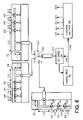
- FIG. 2 illustrates the configuration of an inverted-F antenna 500 and its associated components, which can be used for the inverted-F antennas 52 , 54 and 56 shown in FIG. 1 , in accordance with an embodiment of the invention.
- the inverted-F antenna 500 includes: an inverted F-shaped main conductive element 502 for RF signal radiation and reception; elongated rectangular conductive elements 506 and 508 located at intermediate positions of the antenna 500 and an elongated rectangular conductive element 510 located at a distal end of the antenna 500 ; and a grounding metal conductor 518 .
- the conductive elements 506 - 510 are coupled in series to the element 502 and used for radiation and reception of RF electromagnetic waves.
- the elements 502 , 506 , 508 and 510 are mounted as a formed plate on a printed circuit board 400 or formed as strip lines on it.
- the inverted-F antenna further includes switching units 602 , 604 and 606 which are mounted on the printed circuit board 400 and used for tuning or adjusting the effective length L or the resonance frequency f of the antenna 500 .
- the inverted F-shaped main element 502 is made up of a long narrow segment 504 , a short base segment 512 branching out downward and substantially vertically from one end of the segment 504 and connected at a ground point GP to the grounding conductor 518 , and a short feeder segment 514 branching out downward and substantially vertically from the segment 504 at an intermediate point between the two ends thereof, and separated or spaced from the grounding conductor 518 .
- the segment 504 and the elements 506 , 508 and 510 are arranged in a substantially straight line, extending substantially parallel to the upper edge of the grounding conductor 518 that is closer to element 502 .
- the feeder element 514 is coupled at its end or feed point FP to a feeder line or RF signal line 520 , such as a coaxial cable.
- the switching unit 602 is coupled between the other end of the segment 504 and one end of the element 506 .
- the switching unit 604 is coupled between the other end of the element 506 and one end of the element 508 .
- the switching unit 606 is coupled between the other end of the element 508 and one end of the element 510 .
- the effective length L of the inverted-F antenna 500 is represented by the sum of the combined lengths of the segments 512 and 504 of the element 502 and the combined lengths of the elements 506 to 510 electrically coupled to the element 502 .
- the length of each of the elements 504 to 514 is typically in the order of about 1 cm to about 10 cm.
- the switching units 602 , 604 and 606 are shown exaggerated in size for illustrative purposes, but actually they are much smaller in dimensions or in size than the elements 502 and 506 to 510 , and each of dimensions of the switching units is about one to a few milli-meters for example.
- VSWR voltage standing wave ratio
- the value of VSWR is one (1).
- the value of VSWR is made somewhat larger than one, the quality of the RF signal is degraded somewhat, but the range of resonance frequencies of the antenna 500 becomes wider.
- the information processing apparatus 10 further includes a signal processor 302 , an RF tuner 304 and a control decoder 306 .
- the signal processor 302 may be a processor generally used in personal computers and the like, which includes a CPU, a ROM, a RAM and the like.
- the signal processor 302 is coupled to the RF tuner 304 and the control decoder 306 .
- the RF tuner 304 is coupled to the feeder line 520 .
- the control decoder 306 is coupled to the switching units 602 to 606 of the antenna 500 .
- the signal processor 302 provides data representative of a channel identification or a channel number to the RF tuner 304 , and also provides, to the control decoder 306 , a control signal for tuning the resonance frequency f of the antenna 500 that corresponds to the channel identification.
- the control decoder 306 decodes the control signal to generate further control signals suitable for controlling the switching units 602 to 606 , and provide the thus generated ON/OFF control signals SC 1 , SC 2 and SC 3 to the respective switching units 602 to 606 .
- the control signal provided to the control decoder 306 may contain ON/OFF control instructions for the respective switching units 602 to 606 .
- the control decoder 306 may receive the channel identification as the control signal, and decode the channel identification to generate the further control signals suitable for controlling the switching units 602 to 606 .
- the switching unit 602 couples or decouples the element 502 to or from the element 506 to thereby determine the effective length L or the resonance frequency f of the antenna 500 .
- the switching unit 604 further couples or decouples the element 506 to or from the element 508 to thereby determine the effective length L or the resonance frequency f of the antenna 500 .
- the switching unit 606 further couples or decouples the element 508 to or from the element 510 to thereby determine the effective length L or the resonance frequency f of the antenna 500 .
- the units 602 to 606 are single-pole single-throw switches.
- the effective length L of the antenna 500 is the sum of the length L 1 of the segment 512 and the length L 2 of the segment 504 , i.e., the antenna length L 1 +L 2 of the main conductive element 502 .
- the effective length L of the antenna 500 is the sum of the length L 1 +L 2 of the element 502 and the length L 3 of the element 506 .
- the effective length L of the antenna 500 is the sum of the length L 1 +L 2 of the element 502 , the length L 3 of the element 506 and the length L 4 of the element 508 .
- the effective length L of the antenna 500 is the sum of the length L 1 +L 2 of the element 502 , the length L 3 of the element 506 , the length L 4 of the element 508 and the length L 5 of the element 510 .
- the transmission/reception frequency band of the antenna 500 can be varied in this manner.
- the effective length L of the antenna 500 is approximately equal to one quarter of the wavelength ⁇ of the transmitted or received RF signal.
- a small inverted-F antenna having a wider frequency range can be provided using simple digital circuitry for turning the switches on and off.
- FIG. 3 illustrates the configuration of an inverted-F antenna 700 and its associated components which can be used for the inverted-F antennas 52 , 54 and 56 shown in FIG. 1 , in accordance with another embodiment of the invention.
- the inverted-F antenna 700 similarly to the one shown in FIG. 2 , includes the inverted F-shaped main conductive element 502 , the elongated rectangular conductive elements 506 , 508 and 510 , and the grounding metal conductor 518 .
- the inverted-F antenna 700 further includes switching and tuning units 612 , 614 and 616 for tuning the effective length L or the resonance frequency f of the antenna 700 , and a further conductive segment 516 containing an impedance or resonance frequency tuning unit 651 for matching the impedance of the antenna 700 to that of the feeder line 520 , for example 50 ⁇ .
- the switch SW 1 in the unit 612 takes one of three positions, i.e., the position of a bypass or short-circuiting terminal a 1 coupled to the element 506 , the position of a terminal b 1 coupled to an LC resonant circuit which in turn is coupled to the element 506 , and the position of a neutral state n 1 which is the OFF state in which a pole of the switch SW 1 is coupled to neither of the terminals a 1 and b 1 . That is, the switch SW 1 is a single-pole double-throw switch having the neutral position.
- the terminal a 1 is provided for coarse tuning of the effective length L or the resonance frequency f of the antenna 700 .
- the LC resonant circuit is formed by an inductor L 11 and a variable capacitor C 11 coupled in series, and is provided for fine tuning of the effective length L or the resonance frequency f.
- the impedance of an inductor and a variable capacitor coupled in series takes a minimum value at the resonance frequency.
- the switch SW 2 in the unit 614 takes one of three positions, i.e., the position of a terminal a 2 coupled to the element 508 , the position of a terminal b 2 coupled to an LC resonant circuit which in turn is coupled to the element 508 , and the position of a neutral state n 2 which is the OFF state in which a pole of the switch SW 2 is coupled to neither of the terminals a 2 and b 2 .
- the terminal a 2 is provided for coarse tuning of the effective length L or the resonance frequency f of the antenna 700 .
- the LC resonant circuit is formed by an inductor L 12 and a variable capacitor C 12 coupled in series, and is provided for fine tuning of the effective length L or the resonance frequency f.
- the switch SW 3 in the unit 616 takes one of three positions, i.e., the position of a terminal a 3 coupled to the element 510 , the position of a terminal b 3 coupled to an LC resonant circuit which in turn is coupled to the element 510 , or the position of a neutral state n 3 which is the OFF state in which a pole of the switch SW 3 is coupled to neither of the terminals a 3 and b 3 .
- the terminal a 3 is provided for coarse tuning of the effective length L or the resonance frequency f of the antenna 700 .
- the LC resonant circuit is formed by an inductor L 13 and a variable capacitor C 13 coupled in series, and is provided for fine tuning of the effective length L or the resonance frequency f.
- the conductive segment 516 of the inverted F-shaped main element 502 branches out substantially vertically from the segment 504 at a position intermediate between the segments 512 and 514 , and is connected to the grounding conductor 518 .
- the tuning unit 651 is disposed halfway in the conductive segment 516 between its two separated portions, i.e., one separated segment portion connected to the segment 504 and the other separated segment portion connected to the grounding conductor 518 .
- the tuning unit 651 is coupled in series to the segment 516 .
- the tuning unit 651 includes an LC resonant circuit which is formed by an inductor L 01 and a variable capacitor C 01 coupled in series.
- the tuning unit 651 is provided so as to match the impedance of the antenna 700 to that of the feeder line 520 when the resonance frequency is tuned by the units 612 to 616 , and thus to prevent impedance mismatch from occurring and from causing VSWR to vary when the resonance frequency is tuned by the units 612 to 616 .
- the switches SW 1 to SW 3 , inductors L 11 to L 13 , and variable capacitors C 11 to C 13 in the respective units 612 , 614 and 616 , as well as the inductor L 01 and variable capacitor C 01 in the unit 651 , are shown exaggerated in size for illustrative purposes, but actually they are much smaller in dimensions or size than the elements 502 and 506 to 510 , and each of dimensions of the inductors and capacitors is about one to a few millimeters for example.
- the signal processor 302 similarly to the one shown in FIG. 2 , provides data representative of a channel identification to the RF tuner 304 , and also provides, to the control decoder 306 , a control signal for tuning the resonance frequency f of the antenna 700 that corresponds to the channel identification.
- the control decoder 306 decodes the control signal to generate further control signals suitable for controlling the units 612 to 651 , and provide the thus generated digital ON/OFF control signals SC 1 , SC 2 and SC 3 and also analog variable capacitor control voltage signals CS 1 to CS 3 and CS 0 to the respective units 612 to 651 .
- the control decoder 306 includes a digital-analog converter for generating the control signals CS 1 to CS 3 and CS 0 .
- the control signal provided to the control decoder 306 may include ON/OFF control instructions for the respective switching units 612 to 616 .
- the control decoder 306 may receive the channel identification as the control signal, and decode the channel identification to generate the further control signals suitable for controlling the units 612 to 651 .
- the unit 612 coarsely tunes the effective length L or the resonance frequency f of the antenna 700 , by coupling the switch SW 1 to the position of the terminal a 1 or b 1 or the position of the OFF state n 1 to thereby couple the element 502 to the element 506 or to the LC resonant circuit formed by the devices L 11 and C 11 coupled to the element 506 or decouple the element 502 from them.
- the unit 612 finely tunes the effective length L or the resonance frequency f of the antenna 700 in response to the analog control signal CS 1 , by controlling the variable capacitance of the variable capacitor C 11 to thereby finely tune the resonance frequency of the LC resonant circuit.
- the unit 614 coarsely tunes the effective length L or the resonance frequency f of the antenna 700 in response to the control signal SC 2 , by coupling the switch SW 2 to the position of the terminal a 2 or b 2 or the position of the OFF state n 2 to thereby couple the element 506 to the element 508 or to the LC resonant circuit formed by the elements L 12 and C 12 coupled to the element 508 , or decouple the switch SW 2 from them.
- the unit 614 finely tunes the effective length L or the resonance frequency f of the antenna 700 in response to the analog control signal CS 2 , by controlling the variable capacitance of the variable capacitor C 12 to thereby finely tune the resonance frequency of the LC resonant circuit.
- the unit 616 coarsely tunes the effective length L or the resonance frequency f of the antenna 700 in response to the control signal SC 3 , by coupling the switch SW 3 to the position of the terminal a 3 or b 3 or the position of the OFF state n 3 to thereby couple the element 508 to the element 510 or to the LC resonant circuit formed by the elements L 13 and C 13 coupled to the element 510 , or decouple the element 508 from them.
- the unit 616 finely tunes the effective length L or the resonance frequency f of the antenna 700 in response to the analog control signal CS 3 , by controlling the variable capacitance of the variable capacitor C 13 to thereby finely tune the resonance frequency of the LC resonant circuit.
- the unit 651 controls the variable capacitance of the variable capacitor C 01 to tune the resonance frequency of the LC resonant circuit and thereby effectively or virtually vary the distance between the feed point FP and the ground point GP, to thereby match the impedance of the antenna 700 to that of the feeder line 520 .
- the control signal CS 0 is predetermined in accordance with the values of the control signals CS 1 to CS 3 .
- FIG. 4 shows a table representing the relationship of the resonance frequency f of the inverted-F antenna 700 relative to the positions of the switches SW 1 to SW 3 in the switching and tuning units 612 to 616 , and the values Z's of the impedance of the LC resonant circuits containing the variable capacitors C 11 to C 13 , respectively.
- the resonance frequency f increases substantially monotonically from f( 1 ) to f( 13 ).
- the switches SW 1 , SW 2 and SW 3 select the positions of the terminals a 1 , a 2 and a 3 , respectively, i.e., the short-circuiting positions. Accordingly, all of the elements 506 to 510 are coupled to the element 502 of the antenna 700 , so that the length L of the antenna 700 becomes the longest (L 1 +L 2 +L 3 +L 4 +L 5 ). Thus the resonance frequency f becomes the lowest, i.e., f( 1 ).
- the switches SW 1 and SW 2 select the positions of the terminals a 1 and a 2 , respectively, while the switch SW 3 selects the position of the terminal b 3 . Accordingly, the elements 506 and 508 are coupled to the element 502 of the antenna 700 , and the LC resonant circuit formed by the inductor L 13 and capacitor C 13 in the unit 616 is coupled between the elements 508 and 510 .
- the switches SW 1 and SW 2 select the positions of the terminals a 1 and a 2 , respectively, while the switch SW 3 selects the OFF position. Accordingly, the elements 506 and 508 are coupled to the element 502 of the antenna 700 , so that the length L of the antenna 700 is L 1 +L 2 +L 3 +L 4 . Thus the resonance frequency f becomes f( 5 ).
- the switch SW 1 selects the position of the terminal a 1
- the switch SW 2 selects the position of the terminal b 2
- the switch SW 3 selects the OFF position. Accordingly, the element 506 is coupled to the element 502 of the antenna 700 , and the LC resonant circuit formed by the inductor L 12 and capacitor C 12 in the unit 614 is coupled between the elements 506 and 508 .
- the switch SW 1 selects the position of the terminal a 1 , while each of the switches SW 2 and SW 3 selects the OFF position. Accordingly, the element 506 is coupled to the element 502 of the antenna 700 , so that the length L of the antenna 700 is L 1 +L 2 +L 3 . Thus the resonance frequency f becomes f( 9 ).
- the switch SW 1 selects the position of the terminal b 1 , while each of the switches SW 2 and SW 3 selects the OFF position. Accordingly, the LC resonant circuit formed by the inductor L 11 and capacitor C 11 in the unit 602 is coupled between the elements 502 and 506 .
- the impedance Z of the LC resonant circuit is increased, to thereby decouple the element 506 from the element 502 and reduce the effective length L of the antenna 700 .
- the resonance frequency f of the antenna 700 can be increased to f( 11 ) and then f( 12 ).
- the resonance frequency f( 12 ) when the impedance Z is the largest is equal to the resonance frequency f( 13 ) when the switch SW 1 is in the OFF state (State 13 ).
- each of the switches SW 1 , SW 2 and SW 3 selects the OFF position. Accordingly, the antenna 700 includes only the element 502 , so that the length L of the antenna 700 is L 1 +L 2 . Thus the resonance frequency f becomes a maximum value, i.e., f( 13 ).
- the resonance frequency f( 2 ) is approximately equal to f( 1 ), and the resonance frequency f( 4 ) is approximately equal to f( 5 ).
- the terminal a 1 may be eliminated so that the switch SW 1 takes either the position of the terminal b 1 or the position of the OFF state n 1
- the position of the OFF state n 1 may be eliminated so that the switch SW 1 takes either one of the positions of the terminals a 1 and b 1
- the switch SW 1 and the terminal a 1 may be eliminated and the other end of the segment 504 may be coupled permanently or fixedly to the terminal b 1 .
- the resonance frequency f( 6 ) is approximately equal to f( 5 ), and the resonance frequency f( 8 ) is approximately equal to f( 9 ).
- the terminal a 2 may be eliminated so that the switch SW 2 takes either the position of the terminal b 2 or the position of the OFF state n 2
- the position of the OFF state n 2 may be eliminated so that the switch SW 2 takes either one of the positions of the terminals a 2 and b 2
- the switch SW 2 and the terminal a 2 may be eliminated and the other end of the element 506 may be coupled permanently to the terminal b 2 .
- the resonance frequency f( 10 ) is approximately equal to f( 9 ), and the resonance frequency f( 12 ) is approximately equal to f( 13 ).
- the terminal a 3 may be eliminated so that the switch SW 3 takes either the position of the terminal b 3 or the position of the OFF state n 3
- the position of the OFF state n 3 may be eliminated so that the switch SW 3 takes either one of the positions of the terminals a 3 and b 3
- the switch SW 3 and the terminal a 3 may be eliminated and the other end of the element 508 may be coupled permanently to the terminal b 3 .
- the switches SW 1 , SW 2 and SW 3 and the variable capacitors C 11 to C 13 in the respective LC resonant circuits are controlled, and thereby the resonance frequency f of the antenna 700 can be varied over the range of f( 1 ) to f( 13 ).
- a wide frequency tuning range can thus be obtained.
- the values of the inductors L 11 to L 13 and the capacitors C 11 to C 13 are determined so that the relation among variable resonance frequencies f 11 >f 12 >f 13 is established, where f 11 represents the variable resonance frequency of the LC resonant circuit formed by the inductor L 11 and capacitor C 11 , f 12 represents the variable resonance frequency of the LC resonant circuit formed by the inductor L 12 and capacitor C 12 , and f 13 represents the variable resonance frequency of the LC resonant circuit formed by the inductor L 13 and capacitor C 13 .
- the unit 651 optimizes the impedance matching of the antenna 700 by controlling the variable capacitance of the variable capacitor C 01 in response to the control signal CS 0 to thereby effectively or virtually vary the distance from the feed point FP to the ground point GP.
- a plurality of LC resonant circuits containing switches and coupled in series which are similar to those of the units 612 to 616 , may be coupled in series with the segment 516 , and the tuning range for impedance matching may be expanded by controlling them in the same manner as the units 612 to 616 .
- FIG. 5 shows the tuning ranges of the resonance frequency f and the VSWR in accordance with the embodiment of FIG. 3 .
- FIG. 6 illustrates the configuration of an inverted-F antenna 800 and its associated components which can be used for the inverted-F antennas 52 , 54 , and 56 shown in FIG. 1 , in accordance with a further embodiment of the invention.
- the inverted-F antenna 800 similarly to the one shown in FIGS. 2 and 3 , includes the inverted F-shaped main conductive element 502 , the elongated rectangular conductive elements 506 , 508 and 510 , and the grounding metal conductor 518 .
- the inverted-F antenna 800 further includes switching and tuning units 622 , 624 and 626 for tuning the effective length L or the resonance frequency f of the antenna 800 , and a further conductive segment 516 containing an impedance or resonance frequency tuning unit 652 for matching the impedance of the antenna 800 to that of the feeder line 520 .
- the units 622 , 624 , 626 and 652 have configurations similar to those of the corresponding units 612 , 614 , 616 and 651 shown in FIG. 6 , except that each LC resonant circuit is formed by an inductor and a capacitor coupled in parallel. Generally, the impedance of an inductor and a variable capacitor coupled in parallel takes a maximum value at the resonance frequency.
- an LC circuit for fine tuning which is formed by an inductor L 21 and a variable capacitor C 21 coupled in parallel, is coupled between the terminal b 1 and the element 506 .
- an LC circuit for fine tuning which is formed by an inductor L 22 and a variable capacitor C 22 coupled in parallel, is coupled between the terminal b 2 and the element 508 .
- an LC circuit for fine tuning which is formed by an inductor L 23 and a variable capacitor C 23 coupled in parallel, is coupled between the terminal b 3 and the element 510 .
- the tuning unit 652 includes an LC resonant circuit formed by an inductor L 02 and a variable capacitor C 02 coupled in parallel. Similarly to the unit 651 in FIG. 3 , the tuning unit 652 is provided for matching the impedance of the antenna 800 to that of the feeder line 520 when the resonance frequency is tuned by the units 622 to 626 .
- FIG. 7 shows a table representing the relationship of the resonance frequency f of the inverted-F antenna 800 relative to the positions of the switches SW 1 to SW 3 in the switching and tuning units 622 to 626 , and the values Z's of the impedance of the LC resonant circuits containing the variable capacitors C 21 to C 23 , respectively.
- the resonance frequency f increases substantially monotonically from f( 1 ) to f( 13 ).
- the switches SW 1 , SW 2 and SW 3 select the positions of the terminals a 1 , a 2 and a 3 , respectively.
- the length L of the antenna 800 becomes the longest (L 1 +L 2 +L 3 +L 4 +L 5 ).
- the resonance frequency f becomes the lowest, i.e., f( 1 ).
- the switches SW 1 and SW 2 select the positions of the terminals a 1 and a 2 , respectively, while the switch SW 3 selects the position of the terminal b 3 . Accordingly, the elements 506 and 508 are coupled to the element 502 of the antenna 800 , and the LC resonant circuit formed by the inductor L 23 and capacitor C 23 in the unit 626 is coupled between the elements 508 and 510 .
- the impedance Z of the LC resonant circuit is increased, to thereby decouple the element 510 from the element 508 and reduce the effective length L of the antenna 800 .
- the resonance frequency f of the antenna 800 can be increased to f( 2 ) and then to f( 3 ).
- the impedance Z of the LC resonant circuit is set to a maximum value, to thereby decouple the element 510 from the element 508 .
- the resonance frequency f( 4 ) then is approximately equal to the resonance frequency f( 5 ) when the switch SW 3 is in the OFF state (State 5 ).
- the switches SW 1 and SW 2 select the positions of the terminals a 1 and a 2 , respectively, while the switch SW 3 selects the OFF position. Accordingly, the elements 506 and 508 are coupled to the element 502 of the antenna 800 , so that the length L of the antenna 800 becomes L 1 +L 2 +L 3 +L 3 . Thus the resonance frequency f becomes f( 5 ).
- the switch SW 1 selects the position of the terminal a 1
- the switch SW 2 selects the position of the terminal b 2
- the switch SW 3 selects the OFF position. Accordingly, the element 506 is coupled to the element 502 of the antenna 800 , and the LC resonant circuit formed by the inductor L 22 and capacitor C 22 in the unit 624 is coupled between the elements 506 and 508 .
- the impedance Z of the LC resonant circuit is set to a maximum, to thereby decouple the element 508 from the element 506 .
- the resonance frequency f( 8 ) then is approximately equal to the resonance frequency f( 9 ) when the switch SW 2 is in the OFF state (State 9 ).
- the switch SW 1 selects the position of the terminal a 1 , while each of the switches SW 2 and SW 3 selects the OFF position. Accordingly, the element 506 is coupled to the element 502 of the antenna 800 . Thus the resonance frequency f becomes f( 9 ).
- the switch SW 1 selects the position of the terminal b 1 , while each of the switches SW 2 and SW 3 selects the OFF position. Accordingly, the LC resonant circuit formed by the inductor L 21 and capacitor C 21 is coupled between the elements 502 and 506 .
- the impedance Z of the LC resonant circuit is set to a maximum value, to thereby decouple the element 506 from the element 502 .
- the resonance frequency f( 12 ) then is approximately equal to the resonance frequency f( 13 ) when the switch SW 1 is in the OFF state (State 13 ).
- each of the switches SW 1 , SW 2 and SW 3 selects the OFF position. Accordingly, the resonance frequency f of the antenna 800 becomes a maximum value, i.e., f( 13 ).
- the values of the inductors L 21 to L 23 and the capacitors C 21 to C 23 are determined so that the relationship among the resonance frequencies f 21 >f 22 >f 23 is established, where f 21 represents the variable resonance frequency of the LC resonant circuit formed by the inductor L 21 and capacitor C 21 , f 22 represents the variable resonance frequency of the LC resonant circuit formed by the inductor L 22 and capacitor C 22 , and f 23 represents the variable resonance frequency of the LC resonant circuit formed by the inductor L 23 and capacitor C 23 .
- the terminal a 1 may be eliminated so that the switch SW 1 takes either the position of the terminal b 1 or the position of the OFF state n 1
- the position of the OFF state n 1 may be eliminated so that the switch SW 1 takes either one of the positions of the terminals a 1 and b 1
- the switch SW 1 and the terminal a 1 may be eliminated and the other end of the segment 504 may be coupled permanently to the terminal b 1 .
- the terminal a 2 may be eliminated so that the switch SW 2 takes either the position of the terminal b 2 or the position of the OFF state n 2
- the position of the OFF state n 2 may be eliminated so that the switch SW 2 takes either one of the positions of the terminals a 2 and b 2
- the switch SW 2 and the terminal a 2 may be eliminated and the other end of the element 506 may be coupled permanently to the terminal b 2 .
- the terminal a 3 may be eliminated so that the switch SW 3 takes either the position of the terminal b 3 or the position of the OFF state n 3
- the position of the OFF state n 3 may be eliminated so that the switch SW 3 takes either one of the positions of the terminals a 3 and b 3
- the switch SW 3 and the terminal a 3 may be eliminated and the other end of the element 508 may be coupled permanently to the terminal b 3 .
- the unit 652 optimizes the impedance matching of the antenna 800 by controlling the variable capacitance of the variable capacitor C 02 in response to the control signal CS 0 and to thereby effectively or virtually vary the distance from the feed point FP to the ground point GP.
- a plurality of LC resonant circuits containing switches and coupled in series which are similar to those of the units 622 to 626 , may be coupled in series with the segment 516 , and the tuning range for impedance matching may be expanded by controlling them in the same manner as the units 622 to 626 .
- FIG. 5 also shows the tuning ranges of the resonance frequency f and the VSWR in accordance with the embodiment of FIG. 6 .
- FIG. 8 illustrates the configuration of the inverted-F antennas 52 , 54 and 56 shown in FIG. 1 and their associated components, in accordance with a still further embodiment of the invention.
- Each of the antennas 52 , 54 and 56 has the same configuration as that of the inverted-F antenna 500 , 700 or 800 shown in FIG. 2 , 3 or 6 .
- the antennas 52 , 54 and 56 are coupled in parallel to the ground point, and are coupled to the RF tuner 304 via their respective feeder lines, via a switch SW 0 , and via a feeder line 522 such as a coaxial cable.
- the switch SW 0 In response to a digital switch control signal SC 0 , the switch SW 0 selectively couples one of the inverted-F antennas 52 , 54 and 56 to the feeder line 522 .
- the signal processor 302 may monitor the transmitting or receiving condition of the RF signal and select one of the inverted-F antennas that exhibits the best transmitting or receiving condition.
- the control decoder 306 provides the switch control signals SC 0 to SW 0 , and also provides the control signals SC 1 , SC 2 , . . . and SC 9 and the like to the respective resonance frequency tuning switching units 652 to 676 .
- the antenna 52 is tuned to provide an effective length within the range from the shortest length (L 1 +L 12 ) to the longest length (L 1 +L 12 +L 13 +L 14 +L 15 ).
- the antenna 54 is tuned to provide an effective length within the range from the shortest length (L 1 +L 22 ) to the longest length (L 1 +L 22 +L 23 +L 24 +L 25 ).
- the antenna 56 is tuned to provide an effective length within the range from the shortest length (L 1 +L 32 ) to the longest length (L 1 +L 32 +L 33 +L 34 +L 35 ).
- FIG. 9 shows the relationship between the variable effective length L and the resonance frequency f for the inverted-F antennas 52 , 54 and 56 shown in FIG. 8 .
- the resonance frequency is 1,250 MHz
- the resonance frequency is 1,071 MHz
- the resonance frequency is 938 MHz
- the resonance frequency is 833 MHz.
- FIG. 10 shows the relationship between the VSWR and the resonant frequencies shown in FIG. 9 .
- the units 602 to 606 in FIG. 2 , the units 612 to 616 and 651 in FIG. 3 , and the units 622 to 626 and 652 in FIG. 6 may be combined properly among them.
- the unit 604 in FIG. 2 may be replaced by the unit 614 in FIG. 3 or the unit 624 in FIG. 6 .
- the unit 616 in FIG. 3 may be replaced by the unit 606 in FIG. 2 or the unit 626 in FIG. 6 .
- the unit 651 in FIG. 2 for example, may be replaced by the unit 652 in FIG. 3 .
Abstract
An inverted-F antenna has at least two antenna conductive elements coupled in series via at least one switch. An antenna apparatus includes control means for controlling the at least one switch.
Description
The present invention relates to an antenna apparatus, and more particularly to an information processing apparatus having an inverted-F antenna.
Some current desktop personal computers include respective television tuner cards. Typically, such a tuner card is connected via a coaxial cable to an antenna for receiving terrestrial broadcast signals and an antenna dish for receiving satellite broadcast signals, both of which are mounted on a rooftop.
For these several years, mobile apparatuses, such as notebook personal computers (PCs) and personal digital assistants (PDAs), having the capabilities of performing wireless communications via respective small size antennas coupled to the apparatuses, such as the wireless LAN communications, the Bluetooth standard short distance wireless communications and the mobile telephone communications, have been spreading widely. Such mobile apparatuses, however, cannot receive the current terrestrial analog television signals in good condition with respective small antennas coupled to the apparatuses. Thus most mobile apparatuses do not include television tuner cards. In the future, however, when terrestrial digital television broadcasting becomes available in Japan, such mobile apparatuses will be able to receive, with respective small antennas, relatively high quality RF signals with carriers modulated with digital image signals. Thus it is expected that, in the future, many mobile apparatuses will have a capability of receiving terrestrial digital television broadcast signals.
In general, however, RF signals of a plurality of terrestrial television broadcasts exhibit lower frequencies and a wider frequency range than those of the wireless LAN communications and other short distance wireless communications. Transmission and reception of RF signals of a plurality of terrestrial television broadcasts require a relatively large size antenna, which cannot be accommodated in a mobile apparatus.
Japanese Patent Application Laid-Open Publication (JP-A) No. HEI 11-251825 discloses a small inverted-F antenna which can be accommodated in a small mobile communication apparatus. This inverted-F antenna has an antenna length equal to one quarter of the wavelength λ of the transmitted and received RF signal, and is suitable for implementing in a mobile communication apparatus. The inverted-F antenna is associated with a resonant circuit for controlling radiator length in accordance with the frequency and also a resonant circuit for controlling the distance between the feed point and the ground in accordance with the frequency.
Typically, in the inverted-F antenna, a variable capacitance diode is employed for a resonant circuit to control its resonance frequency. However, the typical range of tuning capacitance of such a variable capacitor is relatively small. Widening the range of variable capacitance requires an undesirable relatively high control voltage to be applied to the capacitor.
Japanese Patent Application Laid-Open Publication (JP-A) No. HEI 10-284919 discloses a small antenna apparatus for a mobile communication unit for transmitting and receiving a wide range of RF signals. This antenna apparatus includes the antenna proper and a frequency tuning circuit. The tuning circuit includes an arrangement formed by a diode and a capacitor coupled in parallel. The resonance frequency of the antenna is varied by controlling the on/off operation of the diode.
The inventors have recognized the need for an inverted-F antenna, which has a variable capacitor controllable with a relatively low control voltage, and which has a wider frequency range for receiving RF signals of a plurality of terrestrial broadcasts.
An object of the present invention is to provide an inverted-F antenna that has a wider frequency range.
Another object of the invention is to provide tuning of a resonance frequency of an inverted-F antenna with a wider frequency range.
In accordance with an aspect of the present invention, an antenna apparatus includes an inverted-F antenna having at least two antenna conductive elements coupled in series via at least one switch, and control means for controlling the at least one switch.
In accordance with another of the invention, an antenna apparatus includes an inverted-F antenna having at least two antenna conductive elements to be coupled in series via at least one resonant circuit.
In accordance with a further aspect of the invention, an information processing apparatus includes a plurality of such antenna apparatuses, and means for selecting one of the plurality of antenna apparatuses.
In accordance with a still further aspect of the invention, an information processing apparatus includes a plurality of such antenna apparatuses. The plurality of antenna apparatuses are oriented in respective different directions.
In accordance with a still further aspect of the invention, an information processing apparatus includes such an antenna apparatus, and channel changing means for controlling said antenna apparatus in accordance with receiving channel information provided by a user.
According to the invention, an inverted-F antenna that has a wider frequency range can be provided.
Throughout the drawings, similar symbols and numerals indicate similar items and functions.
The inverted F-shaped main element 502 is made up of a long narrow segment 504, a short base segment 512 branching out downward and substantially vertically from one end of the segment 504 and connected at a ground point GP to the grounding conductor 518, and a short feeder segment 514 branching out downward and substantially vertically from the segment 504 at an intermediate point between the two ends thereof, and separated or spaced from the grounding conductor 518. The segment 504 and the elements 506, 508 and 510 are arranged in a substantially straight line, extending substantially parallel to the upper edge of the grounding conductor 518 that is closer to element 502. The feeder element 514 is coupled at its end or feed point FP to a feeder line or RF signal line 520, such as a coaxial cable.
The switching unit 602 is coupled between the other end of the segment 504 and one end of the element 506. The switching unit 604 is coupled between the other end of the element 506 and one end of the element 508. The switching unit 606 is coupled between the other end of the element 508 and one end of the element 510.
The effective length L of the inverted-F antenna 500 is represented by the sum of the combined lengths of the segments 512 and 504 of the element 502 and the combined lengths of the elements 506 to 510 electrically coupled to the element 502. The length of each of the elements 504 to 514 is typically in the order of about 1 cm to about 10 cm. The switching units 602, 604 and 606 are shown exaggerated in size for illustrative purposes, but actually they are much smaller in dimensions or in size than the elements 502 and 506 to 510, and each of dimensions of the switching units is about one to a few milli-meters for example.
The shapes of the elements 502, 506, 508 and 510 of the antenna 500 and possibly their associated inductance and capacitance are adjusted so that the voltage standing wave ratio (VSWR) (=(1+|r|)/(1−|r|), where r represents the complex voltage reflection coefficient) of the RF signal on the feeder element 514 becomes equal to an appropriate value, for example, two (2). When the antenna 500 is completely matched to the feeder line 520 in terms of impedance, the value of VSWR is one (1). When the value of VSWR is made somewhat larger than one, the quality of the RF signal is degraded somewhat, but the range of resonance frequencies of the antenna 500 becomes wider.
The information processing apparatus 10 further includes a signal processor 302, an RF tuner 304 and a control decoder 306. The signal processor 302 may be a processor generally used in personal computers and the like, which includes a CPU, a ROM, a RAM and the like. The signal processor 302 is coupled to the RF tuner 304 and the control decoder 306. The RF tuner 304 is coupled to the feeder line 520. The control decoder 306 is coupled to the switching units 602 to 606 of the antenna 500.
The signal processor 302 provides data representative of a channel identification or a channel number to the RF tuner 304, and also provides, to the control decoder 306, a control signal for tuning the resonance frequency f of the antenna 500 that corresponds to the channel identification. The control decoder 306 decodes the control signal to generate further control signals suitable for controlling the switching units 602 to 606, and provide the thus generated ON/OFF control signals SC1, SC2 and SC3 to the respective switching units 602 to 606. The control signal provided to the control decoder 306 may contain ON/OFF control instructions for the respective switching units 602 to 606. Alternatively, the control decoder 306 may receive the channel identification as the control signal, and decode the channel identification to generate the further control signals suitable for controlling the switching units 602 to 606.
In response to the control signal SC1, the switching unit 602 couples or decouples the element 502 to or from the element 506 to thereby determine the effective length L or the resonance frequency f of the antenna 500. In response to the control signal SC2, the switching unit 604 further couples or decouples the element 506 to or from the element 508 to thereby determine the effective length L or the resonance frequency f of the antenna 500. In response to the control signal SC3, the switching unit 606 further couples or decouples the element 508 to or from the element 510 to thereby determine the effective length L or the resonance frequency f of the antenna 500. The units 602 to 606 are single-pole single-throw switches.
When the switching unit 602 is in an OFF state, the effective length L of the antenna 500 is the sum of the length L1 of the segment 512 and the length L2 of the segment 504, i.e., the antenna length L1+L2 of the main conductive element 502. When the switching unit 602 is in an ON state and the switching unit 604 is in an OFF state, the effective length L of the antenna 500 is the sum of the length L1+L2 of the element 502 and the length L3 of the element 506. When the switching units 602 and 604 are in ON states and the switching unit 606 is in an OFF state, the effective length L of the antenna 500 is the sum of the length L1 +L2 of the element 502, the length L3 of the element 506 and the length L4 of the element 508. When the switching units 602 to 606 are in ON states, the effective length L of the antenna 500 is the sum of the length L1+L2 of the element 502, the length L3 of the element 506, the length L4 of the element 508 and the length L5 of the element 510. The transmission/reception frequency band of the antenna 500 can be varied in this manner. The effective length L of the antenna 500 is approximately equal to one quarter of the wavelength λ of the transmitted or received RF signal.
In accordance with the embodiment of FIG. 2 , a small inverted-F antenna having a wider frequency range can be provided using simple digital circuitry for turning the switches on and off.
The switch SW1 in the unit 612 takes one of three positions, i.e., the position of a bypass or short-circuiting terminal a1 coupled to the element 506, the position of a terminal b1 coupled to an LC resonant circuit which in turn is coupled to the element 506, and the position of a neutral state n1 which is the OFF state in which a pole of the switch SW1 is coupled to neither of the terminals a1 and b1. That is, the switch SW1 is a single-pole double-throw switch having the neutral position. The terminal a1 is provided for coarse tuning of the effective length L or the resonance frequency f of the antenna 700. The LC resonant circuit is formed by an inductor L11 and a variable capacitor C11 coupled in series, and is provided for fine tuning of the effective length L or the resonance frequency f. Generally, the impedance of an inductor and a variable capacitor coupled in series takes a minimum value at the resonance frequency.
Similarly, the switch SW2 in the unit 614 takes one of three positions, i.e., the position of a terminal a2 coupled to the element 508, the position of a terminal b2 coupled to an LC resonant circuit which in turn is coupled to the element 508, and the position of a neutral state n2 which is the OFF state in which a pole of the switch SW2 is coupled to neither of the terminals a2 and b2. The terminal a2 is provided for coarse tuning of the effective length L or the resonance frequency f of the antenna 700. The LC resonant circuit is formed by an inductor L12 and a variable capacitor C12 coupled in series, and is provided for fine tuning of the effective length L or the resonance frequency f.
Similarly, the switch SW3 in the unit 616 takes one of three positions, i.e., the position of a terminal a3 coupled to the element 510, the position of a terminal b3 coupled to an LC resonant circuit which in turn is coupled to the element 510, or the position of a neutral state n3 which is the OFF state in which a pole of the switch SW3 is coupled to neither of the terminals a3 and b3. The terminal a3 is provided for coarse tuning of the effective length L or the resonance frequency f of the antenna 700. The LC resonant circuit is formed by an inductor L13 and a variable capacitor C13 coupled in series, and is provided for fine tuning of the effective length L or the resonance frequency f.
The conductive segment 516 of the inverted F-shaped main element 502 branches out substantially vertically from the segment 504 at a position intermediate between the segments 512 and 514, and is connected to the grounding conductor 518. The tuning unit 651 is disposed halfway in the conductive segment 516 between its two separated portions, i.e., one separated segment portion connected to the segment 504 and the other separated segment portion connected to the grounding conductor 518. Thus the tuning unit 651 is coupled in series to the segment 516. The tuning unit 651 includes an LC resonant circuit which is formed by an inductor L01 and a variable capacitor C01 coupled in series. The tuning unit 651 is provided so as to match the impedance of the antenna 700 to that of the feeder line 520 when the resonance frequency is tuned by the units 612 to 616, and thus to prevent impedance mismatch from occurring and from causing VSWR to vary when the resonance frequency is tuned by the units 612 to 616.
The switches SW1 to SW3, inductors L11 to L13, and variable capacitors C11 to C13 in the respective units 612, 614 and 616, as well as the inductor L01 and variable capacitor C01 in the unit 651, are shown exaggerated in size for illustrative purposes, but actually they are much smaller in dimensions or size than the elements 502 and 506 to 510, and each of dimensions of the inductors and capacitors is about one to a few millimeters for example.
The signal processor 302, similarly to the one shown in FIG. 2 , provides data representative of a channel identification to the RF tuner 304, and also provides, to the control decoder 306, a control signal for tuning the resonance frequency f of the antenna 700 that corresponds to the channel identification. The control decoder 306 decodes the control signal to generate further control signals suitable for controlling the units 612 to 651, and provide the thus generated digital ON/OFF control signals SC1, SC2 and SC3 and also analog variable capacitor control voltage signals CS1 to CS3 and CS0 to the respective units 612 to 651. The control decoder 306 includes a digital-analog converter for generating the control signals CS1 to CS3 and CS0. The control signal provided to the control decoder 306 may include ON/OFF control instructions for the respective switching units 612 to 616. Alternatively, the control decoder 306 may receive the channel identification as the control signal, and decode the channel identification to generate the further control signals suitable for controlling the units 612 to 651.
In response to the control signal SC1, the unit 612 coarsely tunes the effective length L or the resonance frequency f of the antenna 700, by coupling the switch SW1 to the position of the terminal a1 or b1 or the position of the OFF state n1 to thereby couple the element 502 to the element 506 or to the LC resonant circuit formed by the devices L11 and C11 coupled to the element 506 or decouple the element 502 from them. When the switch SW1 is placed on the terminal b1, the unit 612 finely tunes the effective length L or the resonance frequency f of the antenna 700 in response to the analog control signal CS1, by controlling the variable capacitance of the variable capacitor C11 to thereby finely tune the resonance frequency of the LC resonant circuit.
Similarly, the unit 614 coarsely tunes the effective length L or the resonance frequency f of the antenna 700 in response to the control signal SC2, by coupling the switch SW2 to the position of the terminal a2 or b2 or the position of the OFF state n2 to thereby couple the element 506 to the element 508 or to the LC resonant circuit formed by the elements L12 and C12 coupled to the element 508, or decouple the switch SW2 from them. When the switch SW2 is placed on the terminal b2, the unit 614 finely tunes the effective length L or the resonance frequency f of the antenna 700 in response to the analog control signal CS2, by controlling the variable capacitance of the variable capacitor C12 to thereby finely tune the resonance frequency of the LC resonant circuit.
Similarly, the unit 616 coarsely tunes the effective length L or the resonance frequency f of the antenna 700 in response to the control signal SC3, by coupling the switch SW3 to the position of the terminal a3 or b3 or the position of the OFF state n3 to thereby couple the element 508 to the element 510 or to the LC resonant circuit formed by the elements L13 and C13 coupled to the element 510, or decouple the element 508 from them. When the switch SW3 is placed on the terminal b3, the unit 616 finely tunes the effective length L or the resonance frequency f of the antenna 700 in response to the analog control signal CS3, by controlling the variable capacitance of the variable capacitor C13 to thereby finely tune the resonance frequency of the LC resonant circuit.
In response to the analog control signal CS0, the unit 651 controls the variable capacitance of the variable capacitor C01 to tune the resonance frequency of the LC resonant circuit and thereby effectively or virtually vary the distance between the feed point FP and the ground point GP, to thereby match the impedance of the antenna 700 to that of the feeder line 520. The control signal CS0 is predetermined in accordance with the values of the control signals CS1 to CS3.
Referring to FIG. 4 , in State 1, the switches SW1, SW2 and SW3 select the positions of the terminals a1, a2 and a3, respectively, i.e., the short-circuiting positions. Accordingly, all of the elements 506 to 510 are coupled to the element 502 of the antenna 700, so that the length L of the antenna 700 becomes the longest (L1+L2+L3+L4+L5). Thus the resonance frequency f becomes the lowest, i.e., f(1).
In States 2 to 4, the switches SW1 and SW2 select the positions of the terminals a1 and a2, respectively, while the switch SW3 selects the position of the terminal b3. Accordingly, the elements 506 and 508 are coupled to the element 502 of the antenna 700, and the LC resonant circuit formed by the inductor L13 and capacitor C13 in the unit 616 is coupled between the elements 508 and 510.
In State 2, by tuning the capacitance of the capacitor C13 so as to cause the LC resonant circuit to become in the resonant state, the impedance Z of the LC resonant circuit is reduced to almost zero, substantially the same state as State 1. Thus the resonance frequency f becomes f(2)≅f(1).
In States 3 and 4, by tuning the capacitance of the capacitor C13 so as to cause the LC resonant circuit to become in a non-resonant state, the impedance Z of the LC resonant circuit is increased and the element 510 is decoupled from the element 508. Thus the effective length L of the antenna 700 is reduced. In this way, the resonance frequency f of the antenna 700 can be increased to f(3) and then to f(4). The resonance frequency f(4) when the impedance Z is the largest is approximately equal to the resonance frequency f(5) when the switch SW3 is in the OFF state (State 5).
In State 5, the switches SW1 and SW2 select the positions of the terminals a1 and a2, respectively, while the switch SW3 selects the OFF position. Accordingly, the elements 506 and 508 are coupled to the element 502 of the antenna 700, so that the length L of the antenna 700 is L1+L2+L3+L4. Thus the resonance frequency f becomes f(5).
In States 6 to 8, the switch SW1 selects the position of the terminal a1, the switch SW2 selects the position of the terminal b2, and the switch SW3 selects the OFF position. Accordingly, the element 506 is coupled to the element 502 of the antenna 700, and the LC resonant circuit formed by the inductor L12 and capacitor C12 in the unit 614 is coupled between the elements 506 and 508.
In State 6, by tuning the capacitance of the capacitor C12 so as to cause the LC resonant circuit to become in the resonant state, the impedance Z of the LC resonant circuit is reduced to almost zero, substantially the same state as State 5. Thus the resonance frequency f becomes f(6)≅f(5).
In States 7 and 8, by tuning the capacitance of the capacitor C12 so as to cause the LC resonant circuit to become in a non-resonant state, the impedance Z of the LC resonant circuit is increased, to thereby decouple the element 508 from the element 506 and reduce the effective length L of the antenna 700. In this way, the resonance frequency f of the antenna 700 can be increased to f(7) and then to f(8). The resonance frequency f(8) when the impedance Z is the largest is approximately equal to the resonance frequency f(9) when the switch SW2 is in the OFF state (State 9).
In State 9, the switch SW1 selects the position of the terminal a1, while each of the switches SW2 and SW3 selects the OFF position. Accordingly, the element 506 is coupled to the element 502 of the antenna 700, so that the length L of the antenna 700 is L1+L2 +L3. Thus the resonance frequency f becomes f(9).
In States 10 to 12, the switch SW1 selects the position of the terminal b1, while each of the switches SW2 and SW3 selects the OFF position. Accordingly, the LC resonant circuit formed by the inductor L11 and capacitor C11 in the unit 602 is coupled between the elements 502 and 506.
In State 10, by tuning the capacitance of the capacitor C11 so as to cause the LC resonant circuit to become in the resonant state, the impedance Z of the LC resonant circuit is reduced to almost zero, substantially the same state as State 9. Thus the resonance frequency f becomes f(10).
In States 11 and 12, by tuning the capacitance of the capacitor C11 so as to cause the LC resonant circuit to become in a non-resonant state, the impedance Z of the LC resonant circuit is increased, to thereby decouple the element 506 from the element 502 and reduce the effective length L of the antenna 700. In this way, the resonance frequency f of the antenna 700 can be increased to f(11) and then f(12). The resonance frequency f(12) when the impedance Z is the largest is equal to the resonance frequency f(13) when the switch SW1 is in the OFF state (State 13).
In State 13, each of the switches SW1, SW2 and SW3 selects the OFF position. Accordingly, the antenna 700 includes only the element 502, so that the length L of the antenna 700 is L1+L2. Thus the resonance frequency f becomes a maximum value, i.e., f(13).
The resonance frequency f(2) is approximately equal to f(1), and the resonance frequency f(4) is approximately equal to f(5). Thus, in the unit 612, the terminal a1 may be eliminated so that the switch SW1 takes either the position of the terminal b1 or the position of the OFF state n1, the position of the OFF state n1 may be eliminated so that the switch SW1 takes either one of the positions of the terminals a1 and b1, or the switch SW1 and the terminal a1 may be eliminated and the other end of the segment 504 may be coupled permanently or fixedly to the terminal b1.
Similarly, the resonance frequency f(6) is approximately equal to f(5), and the resonance frequency f(8) is approximately equal to f(9). Thus, in the unit 614, the terminal a2 may be eliminated so that the switch SW2 takes either the position of the terminal b2 or the position of the OFF state n2, the position of the OFF state n2 may be eliminated so that the switch SW2 takes either one of the positions of the terminals a2 and b2, or the switch SW2 and the terminal a2 may be eliminated and the other end of the element 506 may be coupled permanently to the terminal b2.
Similarly, the resonance frequency f(10) is approximately equal to f(9), and the resonance frequency f(12) is approximately equal to f(13). Thus, in the unit 616, the terminal a3 may be eliminated so that the switch SW3 takes either the position of the terminal b3 or the position of the OFF state n3, the position of the OFF state n3 may be eliminated so that the switch SW3 takes either one of the positions of the terminals a3 and b3, or the switch SW3 and the terminal a3 may be eliminated and the other end of the element 508 may be coupled permanently to the terminal b3.
In this way, the switches SW1, SW2 and SW3 and the variable capacitors C11 to C13 in the respective LC resonant circuits are controlled, and thereby the resonance frequency f of the antenna 700 can be varied over the range of f(1) to f(13). Thus a wide frequency tuning range can thus be obtained.
The values of the inductors L11 to L13 and the capacitors C11 to C13 are determined so that the relation among variable resonance frequencies f11>f12>f13 is established, where f11 represents the variable resonance frequency of the LC resonant circuit formed by the inductor L11 and capacitor C11, f12 represents the variable resonance frequency of the LC resonant circuit formed by the inductor L12 and capacitor C12, and f13 represents the variable resonance frequency of the LC resonant circuit formed by the inductor L13 and capacitor C13.
When proper impedance matching of the antenna 700 cannot be achieved by controlling the switches SW1, SW2 and SW3 and the variable capacitors C11 to C13 in the respective LC resonant circuits, and consequently the VSWR increases undesirably, the unit 651 optimizes the impedance matching of the antenna 700 by controlling the variable capacitance of the variable capacitor C01 in response to the control signal CS0 to thereby effectively or virtually vary the distance from the feed point FP to the ground point GP. Alternatively, in place of the unit 651, a plurality of LC resonant circuits containing switches and coupled in series, which are similar to those of the units 612 to 616, may be coupled in series with the segment 516, and the tuning range for impedance matching may be expanded by controlling them in the same manner as the units 612 to 616.
The units 622, 624, 626 and 652 have configurations similar to those of the corresponding units 612, 614, 616 and 651 shown in FIG. 6 , except that each LC resonant circuit is formed by an inductor and a capacitor coupled in parallel. Generally, the impedance of an inductor and a variable capacitor coupled in parallel takes a maximum value at the resonance frequency.
In the unit 622, an LC circuit for fine tuning, which is formed by an inductor L21 and a variable capacitor C21 coupled in parallel, is coupled between the terminal b1 and the element 506. In the unit 624, an LC circuit for fine tuning, which is formed by an inductor L22 and a variable capacitor C22 coupled in parallel, is coupled between the terminal b2 and the element 508. In the unit 626, an LC circuit for fine tuning, which is formed by an inductor L23 and a variable capacitor C23 coupled in parallel, is coupled between the terminal b3 and the element 510. The tuning unit 652 includes an LC resonant circuit formed by an inductor L02 and a variable capacitor C02 coupled in parallel. Similarly to the unit 651 in FIG. 3 , the tuning unit 652 is provided for matching the impedance of the antenna 800 to that of the feeder line 520 when the resonance frequency is tuned by the units 622 to 626.
Referring to FIG. 7 , similarly to the table shown in FIG. 4 , in State 1, the switches SW1, SW2 and SW3 select the positions of the terminals a1, a2 and a3, respectively. In this state, the length L of the antenna 800 becomes the longest (L1+L2+L3+L4 +L5). Thus the resonance frequency f becomes the lowest, i.e., f(1).
In States 2 to 4, the switches SW1 and SW2 select the positions of the terminals a1 and a2, respectively, while the switch SW3 selects the position of the terminal b3. Accordingly, the elements 506 and 508 are coupled to the element 502 of the antenna 800, and the LC resonant circuit formed by the inductor L23 and capacitor C23 in the unit 626 is coupled between the elements 508 and 510.
In States 2 and 3, by tuning the capacitance of the capacitor C23 so as to cause the LC resonant circuit to become in a non-resonant state, the impedance Z of the LC resonant circuit is increased, to thereby decouple the element 510 from the element 508 and reduce the effective length L of the antenna 800. Thus the resonance frequency f of the antenna 800 can be increased to f(2) and then to f(3).
In State 2, by tuning the capacitance of the capacitor C23 so as to cause the LC resonant circuit to become in a non-resonant state, the impedance Z of the LC resonant circuit is set to a minimum value, substantially the same state as State 1. Thus the resonance frequency f becomes f(2)≅f(1).
In State 4, by tuning the capacitance of the capacitor C23 so as to cause the LC resonant circuit to become in the resonant state, the impedance Z of the LC resonant circuit is set to a maximum value, to thereby decouple the element 510 from the element 508. The resonance frequency f(4) then is approximately equal to the resonance frequency f(5) when the switch SW3 is in the OFF state (State 5).
In State 5, the switches SW1 and SW2 select the positions of the terminals a1 and a2, respectively, while the switch SW3 selects the OFF position. Accordingly, the elements 506 and 508 are coupled to the element 502 of the antenna 800, so that the length L of the antenna 800 becomes L1+L2+L3+L3. Thus the resonance frequency f becomes f(5).
In States 6 to 8, the switch SW1 selects the position of the terminal a1, the switch SW2 selects the position of the terminal b2, and the switch SW3 selects the OFF position. Accordingly, the element 506 is coupled to the element 502 of the antenna 800, and the LC resonant circuit formed by the inductor L22 and capacitor C22 in the unit 624 is coupled between the elements 506 and 508.
In States 6 and 7, by tuning the capacitance of the capacitor C22 so as to cause the LC resonant circuit to become in a non-resonant state, the impedance Z of the LC resonant circuit is increased, to thereby decouple the element 508 from the element 506 and reduce the effective length L of the antenna 800. Thus the resonance frequency f of the antenna 800 can be increased to f(6) and then to f(7).
In State 6, by tuning the capacitance of the capacitor C22 so as to cause the LC resonant circuit to become in a non-resonant state, the impedance Z of the LC resonant circuit is set to a minimum, substantially the same state as State 5. Thus the resonance frequency f becomes f(6)≅f(5).
In State 8, by tuning the capacitance of the capacitor C22 so as to cause the LC resonant circuit to become in the resonant state, the impedance Z of the LC resonant circuit is set to a maximum, to thereby decouple the element 508 from the element 506. The resonance frequency f(8) then is approximately equal to the resonance frequency f(9) when the switch SW2 is in the OFF state (State 9).
In State 9, the switch SW1 selects the position of the terminal a1, while each of the switches SW2 and SW3 selects the OFF position. Accordingly, the element 506 is coupled to the element 502 of the antenna 800. Thus the resonance frequency f becomes f(9).
In States 10 to 12, the switch SW1 selects the position of the terminal b1, while each of the switches SW2 and SW3 selects the OFF position. Accordingly, the LC resonant circuit formed by the inductor L21 and capacitor C21 is coupled between the elements 502 and 506.
In States 10 and 11, by tuning the capacitance of the capacitor C21 so as to cause the LC resonant circuit to become in a non-resonant state, the impedance Z of the LC resonant circuit is increased, to thereby decouple the element 506 from the element 502 and reduce the effective length L of the antenna 800. Thus the resonance frequency f of the antenna 800 can be increased to f(10) and then to f(11).
In State 10, by tuning the capacitance of the capacitor C21 so as to cause the LC resonant circuit to become in a non-resonant state, the impedance Z of the LC resonant circuit is set to a minimum value, substantially the same state as State 1. Thus the resonance frequency f becomes f(10)≅f(9).
In State 12, by tuning the capacitance of the capacitor C21 so as to cause the LC resonant circuit to become in the resonant state, the impedance Z of the LC resonant circuit is set to a maximum value, to thereby decouple the element 506 from the element 502. The resonance frequency f(12) then is approximately equal to the resonance frequency f(13) when the switch SW1 is in the OFF state (State 13).
In State 13, each of the switches SW1, SW2 and SW3 selects the OFF position. Accordingly, the resonance frequency f of the antenna 800 becomes a maximum value, i.e., f(13).
The values of the inductors L21 to L23 and the capacitors C21 to C23 are determined so that the relationship among the resonance frequencies f21>f22>f23 is established, where f21 represents the variable resonance frequency of the LC resonant circuit formed by the inductor L21 and capacitor C21, f22 represents the variable resonance frequency of the LC resonant circuit formed by the inductor L22 and capacitor C22, and f23 represents the variable resonance frequency of the LC resonant circuit formed by the inductor L23 and capacitor C23.
Similarly to the unit in FIG. 3 , in the unit 622, the terminal a1 may be eliminated so that the switch SW1 takes either the position of the terminal b1 or the position of the OFF state n1, the position of the OFF state n1 may be eliminated so that the switch SW1 takes either one of the positions of the terminals a1 and b1, or the switch SW1 and the terminal a1 may be eliminated and the other end of the segment 504 may be coupled permanently to the terminal b1.
Similarly, in the unit 624, the terminal a2 may be eliminated so that the switch SW2 takes either the position of the terminal b2 or the position of the OFF state n2, the position of the OFF state n2 may be eliminated so that the switch SW2 takes either one of the positions of the terminals a2 and b2, or the switch SW2 and the terminal a2 may be eliminated and the other end of the element 506 may be coupled permanently to the terminal b2.
Similarly, in the unit 626, the terminal a3 may be eliminated so that the switch SW3 takes either the position of the terminal b3 or the position of the OFF state n3, the position of the OFF state n3 may be eliminated so that the switch SW3 takes either one of the positions of the terminals a3 and b3, or the switch SW3 and the terminal a3 may be eliminated and the other end of the element 508 may be coupled permanently to the terminal b3.
Similarly to the unit in FIG. 3 , the unit 652 optimizes the impedance matching of the antenna 800 by controlling the variable capacitance of the variable capacitor C02 in response to the control signal CS0 and to thereby effectively or virtually vary the distance from the feed point FP to the ground point GP. Alternatively, in place of the unit 652, a plurality of LC resonant circuits containing switches and coupled in series, which are similar to those of the units 622 to 626, may be coupled in series with the segment 516, and the tuning range for impedance matching may be expanded by controlling them in the same manner as the units 622 to 626.
In this way, according to the embodiments of FIGS. 3 and 6 , since the LC resonant circuits in the units 612 to 616 and 651 and the units 622 to 626 and 652 are only responsible for fining tuning of the resonance frequency f of the antenna 700 or 800, the capacitance tuning range of the variable capacitor in each LC resonant circuit is small. Thus it requires just a relatively simple analog voltage source for a variable capacitance diode.
In response to a digital switch control signal SC0, the switch SW0 selectively couples one of the inverted- F antennas 52, 54 and 56 to the feeder line 522. The signal processor 302 may monitor the transmitting or receiving condition of the RF signal and select one of the inverted-F antennas that exhibits the best transmitting or receiving condition.
The control decoder 306 provides the switch control signals SC0 to SW0, and also provides the control signals SC1, SC2, . . . and SC9 and the like to the respective resonance frequency tuning switching units 652 to 676.
In response to the control signals SC1 to SC3 and the like, the antenna 52 is tuned to provide an effective length within the range from the shortest length (L1+L12) to the longest length (L1+L12+L13 +L14+L15). In response to the control signals SC4 to SC6 and the like, the antenna 54 is tuned to provide an effective length within the range from the shortest length (L1+L22) to the longest length (L1+L22+L23 +L24+L25). In response to the control signals SC7 to SC9 and the like, the antenna 56 is tuned to provide an effective length within the range from the shortest length (L1+L32) to the longest length (L1+L32+L33 +L34+L35).
The units 602 to 606 in FIG. 2 , the units 612 to 616 and 651 in FIG. 3 , and the units 622 to 626 and 652 in FIG. 6 may be combined properly among them. For example, the unit 604 in FIG. 2 may be replaced by the unit 614 in FIG. 3 or the unit 624 in FIG. 6 . Further, the unit 616 in FIG. 3 , for example, may be replaced by the unit 606 in FIG. 2 or the unit 626 in FIG. 6 . The unit 651 in FIG. 2 , for example, may be replaced by the unit 652 in FIG. 3 .
The above-described embodiments are only typical examples, and their modifications and variations are apparent to those skilled in the art. It should be noted that those skilled in the art can make various modifications to the above-described embodiments without departing from the principle of the invention and the accompanying claims.
Claims (2)
1. An antenna apparatus comprising:
an inverted-F antenna having at least two antenna conductive elements coupled in series via at least one switch, and having at least one switch or variable resonant circuit between one of said at least two antenna conductive elements and the ground for matching the impedance of said inverted-F antenna to the impedance of a feeder line coupled to said inverted-F antenna,
wherein a switch between two adjacent antenna conductive elements of said at least two antenna conductive elements is placed on one of the following three positions:
a first position for coupling a terminal of one of said two adjacent antenna conductive elements directly to a terminal of the other adjacent antenna conductive element,
a second position for coupling the terminal of said one adjacent antenna conductive element via said variable LC resonant circuit to the terminal of said other adjacent antenna conductive element, and
a third position for separating the terminal of said one adjacent antenna conductive element from the terminal of said other adjacent antenna conductive element; and
a controller controlling said at least one switch.
2. An information processing apparatus comprising:
an antenna apparatus comprising an inverted-F antenna having at least two antenna conductive elements coupled in series via at least one switch, and having at least one switch or variable resonant circuit between one of said at least two antenna conductive elements and ground for matching an impedance of said inverted-F antenna to an impedance of a feeder line coupled to said inverted-F antenna,
wherein a switch between two adjacent antenna conductive elements of said at least two antenna conductive elements is placed on one of the following three positions:
a first position for coupling a terminal of one of said two adjacent antenna conductive elements directly to a terminal of the other adjacent antenna conductive element,
a second position for coupling the terminal of said one adjacent antenna conductive element via said variable LO resonant circuit to the terminal of said other adjacent antenna conductive element, and
a third position for separating the terminal of said one adjacent antenna conductive element from the terminal of said other adjacent antenna conductive element, and comprising a controller for controlling said at least one switch; and
a channel changing unit for controlling said antenna apparatus in accordance with receiving channel information provided by a user.
Applications Claiming Priority (2)
| Application Number | Priority Date | Filing Date | Title |
|---|---|---|---|
| JP2002-253729 | 2002-08-30 | ||
| JP2002253729A JP2004096341A (en) | 2002-08-30 | 2002-08-30 | Antenna apparatus including inverted f antenna with variable resonance frequency |
Publications (2)
| Publication Number | Publication Date |
|---|---|
| US20040041734A1 US20040041734A1 (en) | 2004-03-04 |
| US7372406B2 true US7372406B2 (en) | 2008-05-13 |
Family
ID=31972808
Family Applications (1)
| Application Number | Title | Priority Date | Filing Date |
|---|---|---|---|
| US10/639,490 Expired - Fee Related US7372406B2 (en) | 2002-08-30 | 2003-08-13 | Antenna apparatus including inverted-F antenna having variable resonance frequency |
Country Status (2)
| Country | Link |
|---|---|
| US (1) | US7372406B2 (en) |
| JP (1) | JP2004096341A (en) |
Cited By (41)
| Publication number | Priority date | Publication date | Assignee | Title |
|---|---|---|---|---|
| US20080198076A1 (en) * | 2005-07-04 | 2008-08-21 | Mats Andersson | Multi Beam Repeater Antenna for Increased Coverage |
| US20080284662A1 (en) * | 2007-05-17 | 2008-11-20 | Casio Computer Co., Ltd. | Film antenna and electronic equipment |
| US20090073047A1 (en) * | 2005-07-13 | 2009-03-19 | Thomson Licensing Llc | Antenna System With Second-Order Diversity and Card for Wireless Communication Apparatus Which is Equipped With One Such Device |
| US20090079647A1 (en) * | 2007-09-21 | 2009-03-26 | Samsung Electronics Co., Ltd | Multiple Frequency Band Antenna and Antenna system Using the Same |
| US20090167619A1 (en) * | 2007-12-27 | 2009-07-02 | Casio Computer Co., Ltd. | Planar monopole antenna and electronic device |
| US20090231220A1 (en) * | 2008-03-14 | 2009-09-17 | Qualcomm Incorporated | Adaptive tunable antennas for wireless devices |
| US20090295652A1 (en) * | 2008-05-29 | 2009-12-03 | Casio Computer Co., Ltd. | Planar antenna and electronic device |
| US20100026596A1 (en) * | 2008-07-31 | 2010-02-04 | Kabushiki Kaisha Toshiba | Antenna device |
| US20100194647A1 (en) * | 2009-02-05 | 2010-08-05 | Research In Motion Limited | Mobile wireless communications device having diversity antenna system and related methods |
| US20100245195A1 (en) * | 2009-03-31 | 2010-09-30 | Tyco Safety Products Canada Ltd. | Tunable inverted f antenna |
| US20100245198A1 (en) * | 2009-03-31 | 2010-09-30 | Tyco Safety Products Canada Ltd. | Quad-band pcb antenna |
| US20100245201A1 (en) * | 2009-03-30 | 2010-09-30 | Fujitsu Limited | Frequency tunable antenna |
| US20100302111A1 (en) * | 2009-05-27 | 2010-12-02 | Casio Computer Co., Ltd. | Multiband planar antenna and electronic equipment |
| US20110012800A1 (en) * | 2007-08-20 | 2011-01-20 | Ethertronics, Inc. | Antenna with active elements |
| US20110102271A1 (en) * | 2009-11-03 | 2011-05-05 | Asustek Computer Inc. | Wireless transmission device and computer system using the same |
| US20110159832A1 (en) * | 2009-12-28 | 2011-06-30 | Fujitsu Limited | Antenna device and communication device |
| US20110221636A1 (en) * | 2010-03-12 | 2011-09-15 | Advanced Connectek, Inc. | Multiband Antenna |
| US20110260938A1 (en) * | 2010-04-27 | 2011-10-27 | Xie jia-jun | Antenna and antenna assembly using same |
| US20120001821A1 (en) * | 2009-03-19 | 2012-01-05 | Murata Manufacturing Co., Ltd. | Antenna device and wireless communication device |
| US20130234901A1 (en) * | 2012-03-08 | 2013-09-12 | Acer Incorporated | Tunable Slot Antenna |
| US20130257666A1 (en) * | 2007-08-20 | 2013-10-03 | Ethertronics, Inc. | Antenna with multiple coupled regions |
| US20130307732A1 (en) * | 2010-03-12 | 2013-11-21 | Advanced-Connectek Inc. | Multiband antenna |
| WO2014046710A1 (en) * | 2012-09-18 | 2014-03-27 | Ethertronics, Inc. | Antenna system for interference suppression |
| US20140184465A9 (en) * | 2011-06-08 | 2014-07-03 | Panasonic Corporation | Antenna device |
| US20150102969A1 (en) * | 2009-10-21 | 2015-04-16 | The University Of Birmingham | Reconfigurable antenna |
| TWI482356B (en) * | 2011-05-13 | 2015-04-21 | Htc Corp | Handheld device and planar antenna thereof |
| US9166279B2 (en) | 2011-03-07 | 2015-10-20 | Apple Inc. | Tunable antenna system with receiver diversity |
| US9246221B2 (en) | 2011-03-07 | 2016-01-26 | Apple Inc. | Tunable loop antennas |
| US9350069B2 (en) | 2012-01-04 | 2016-05-24 | Apple Inc. | Antenna with switchable inductor low-band tuning |
| US9496608B2 (en) | 2013-04-17 | 2016-11-15 | Apple Inc. | Tunable multiband antenna with passive and active circuitry |
| TWI569509B (en) * | 2012-04-20 | 2017-02-01 | Mitsubishi Materials Corp | Antenna device |
| US9621269B2 (en) | 2012-07-26 | 2017-04-11 | California Institute Of Technology | Optically driven active radiator |
| US9921255B2 (en) | 2012-02-13 | 2018-03-20 | California Institute Of Technology | Sensing radiation metrics through mode-pickup sensors |
| US9941588B2 (en) | 2007-08-20 | 2018-04-10 | Ethertronics, Inc. | Antenna with multiple coupled regions |
| US10128560B2 (en) | 2014-12-12 | 2018-11-13 | Ethertronics, Inc. | Hybrid antenna and integrated proximity sensor using a shared conductive structure |
| US20180337458A1 (en) * | 2017-05-18 | 2018-11-22 | Skyworks Solutions, Inc. | Reconfigurable antenna systems with ground tuning pads |
| US10290944B2 (en) | 2011-10-18 | 2019-05-14 | California Institute Of Technology | Efficient active multi-drive radiator |
| US10892555B2 (en) | 2016-12-12 | 2021-01-12 | Skyworks Solutions, Inc. | Frequency and polarization reconfigurable antenna systems |
| US11158938B2 (en) | 2019-05-01 | 2021-10-26 | Skyworks Solutions, Inc. | Reconfigurable antenna systems integrated with metal case |
| US11942684B2 (en) | 2008-03-05 | 2024-03-26 | KYOCERA AVX Components (San Diego), Inc. | Repeater with multimode antenna |
| US11973283B2 (en) | 2021-02-23 | 2024-04-30 | Skyworks Solutions, Inc. | Reconfigurable antenna systems with ground tuning pads |
Families Citing this family (72)
| Publication number | Priority date | Publication date | Assignee | Title |
|---|---|---|---|---|
| US7746292B2 (en) * | 2001-04-11 | 2010-06-29 | Kyocera Wireless Corp. | Reconfigurable radiation desensitivity bracket systems and methods |
| KR100960570B1 (en) * | 2003-01-06 | 2010-06-03 | 삼성전자주식회사 | Portable computer |
| JPWO2005114778A1 (en) * | 2004-05-21 | 2008-03-27 | 株式会社村田製作所 | Mobile phone equipment |
| JP4444021B2 (en) * | 2004-06-29 | 2010-03-31 | パナソニック株式会社 | Foldable portable radio |
| KR100652667B1 (en) | 2004-09-07 | 2006-12-06 | 엘지전자 주식회사 | Internal antenna control apparatus and method thereof for mobile station |
| JP2006211637A (en) * | 2004-12-27 | 2006-08-10 | Advanced Telecommunication Research Institute International | Array antenna device |
| JP2006186851A (en) * | 2004-12-28 | 2006-07-13 | Toshiba Corp | Antenna system |
| US20060148421A1 (en) * | 2005-01-04 | 2006-07-06 | Via Technologies, Inc. | Method and apparatus for frequency adjustment |
| US7876271B2 (en) | 2005-02-23 | 2011-01-25 | Panasonic Corporation | Antenna unit and portable radio apparatus |
| JP2006235908A (en) * | 2005-02-24 | 2006-09-07 | Toshiba Corp | Electronic apparatus |
| JP2006340095A (en) * | 2005-06-02 | 2006-12-14 | Matsushita Electric Ind Co Ltd | Portable radio device |
| US8532587B2 (en) * | 2005-06-03 | 2013-09-10 | Hewlett-Packard Development Company, L.P. | Usage mode-based antenna selection |
| GB0512281D0 (en) * | 2005-06-16 | 2005-07-27 | Antenova Ltd | Resonant devices to improve antennna performance in handsets and data terminals |
| TWM289264U (en) * | 2005-08-10 | 2006-04-01 | Compal Electronics Inc | Display frame having antenna |
| JP2007159079A (en) | 2005-12-02 | 2007-06-21 | Pantech Co Ltd | Method of automatically compensating sensitivity of mobile communication terminal and mobile communication terminal |
| EP2118966A4 (en) * | 2005-12-12 | 2014-06-04 | Flextronics Ap Llc | Wideband antenna system |
| KR100742097B1 (en) * | 2006-03-20 | 2007-07-24 | 주식회사 이엠따블유안테나 | Dual-band antenna for receiving vhf and uhf signal |
| KR100794788B1 (en) * | 2006-07-20 | 2008-01-21 | 삼성전자주식회사 | Mimo antenna able to operate in multi-band |
| US8781522B2 (en) * | 2006-11-02 | 2014-07-15 | Qualcomm Incorporated | Adaptable antenna system |
| US20080198073A1 (en) * | 2007-02-16 | 2008-08-21 | Mediatek Inc. | Method for adjusting a PCB antenna and a structure thereof |
| JP4790684B2 (en) * | 2007-10-04 | 2011-10-12 | アルプス電気株式会社 | Antenna device |
| US8583197B2 (en) * | 2007-12-12 | 2013-11-12 | Broadcom Corporation | Method and system for sharing antennas for high frequency and low frequency applications |
| US8340714B2 (en) | 2007-12-14 | 2012-12-25 | Microsoft Corporation | Computing device with configurable antenna |
| JP5150369B2 (en) * | 2008-05-28 | 2013-02-20 | 京セラ株式会社 | Communication equipment |
| EP2182577A1 (en) | 2008-10-30 | 2010-05-05 | Laird Technologies AB | An antenna device, an antenna system and a portable radio communication device comprising such an antenna device |
| EP2234207A1 (en) | 2009-03-23 | 2010-09-29 | Laird Technologies AB | Antenna device and portable radio communication device comprising such an antenna device |
| EP2251930A1 (en) | 2009-05-11 | 2010-11-17 | Laird Technologies AB | Antenna device and portable radio communication device comprising such an antenna device |
| TWI514677B (en) * | 2009-07-10 | 2015-12-21 | Chiun Mai Comm Systems Inc | Multiband antenna and wireless communication device using the same |
| CN102577333B (en) * | 2009-10-19 | 2015-04-29 | 联想创新有限公司(香港) | Wireless communication device |
| JP5524580B2 (en) * | 2009-11-12 | 2014-06-18 | 三星電子株式会社 | ANTENNA DEVICE AND WIRELESS COMMUNICATION DEVICE HAVING THE SAME |
| JP5531582B2 (en) * | 2009-11-27 | 2014-06-25 | 富士通株式会社 | Antenna and wireless communication device |
| KR101700744B1 (en) * | 2010-01-29 | 2017-02-01 | 삼성전자주식회사 | Built-in antenna for portable terminal |
| JP5668298B2 (en) * | 2010-03-11 | 2015-02-12 | 株式会社リコー | ANTENNA DEVICE AND WIRELESS COMMUNICATION DEVICE USING THE SAME |
| CN101986463B (en) * | 2010-06-07 | 2014-02-05 | 连展科技电子(昆山)有限公司 | Multi-frequency antenna |
| US9070969B2 (en) | 2010-07-06 | 2015-06-30 | Apple Inc. | Tunable antenna systems |
| US20120086616A1 (en) * | 2010-10-07 | 2012-04-12 | Electronics And Telecommunications Research Institute | Antenna for providing selective radiation patterns and antenna construction method |
| US20120206303A1 (en) | 2010-11-11 | 2012-08-16 | Ethertronics, Inc | Antenna system coupled to an external device |
| FR2967536A1 (en) * | 2010-11-15 | 2012-05-18 | Univ Rennes | COMPACT ANTENNA ADAPTABLE TO IMPEDANCE |
| EP2676325A4 (en) * | 2011-02-14 | 2014-03-12 | Fujitsu Ltd | Multiband antenna |
| WO2012157314A1 (en) * | 2011-05-19 | 2012-11-22 | 株式会社村田製作所 | Antenna device |
| TWI491107B (en) * | 2011-12-20 | 2015-07-01 | Wistron Neweb Corp | Tunable antenna and radio-frequency device |
| US9190712B2 (en) | 2012-02-03 | 2015-11-17 | Apple Inc. | Tunable antenna system |
| US20140080409A1 (en) * | 2012-09-17 | 2014-03-20 | Qualcomm Incorporated | Static tuning of wireless transmitters |
| JP6181507B2 (en) * | 2012-10-24 | 2017-08-16 | 株式会社Soken | antenna |
| US9716307B2 (en) * | 2012-11-08 | 2017-07-25 | Htc Corporation | Mobile device and antenna structure |
| EP2772987B1 (en) * | 2013-02-27 | 2019-07-03 | Samsung Electronics Co., Ltd. | Antenna for camera |
| CN104051853A (en) * | 2013-03-15 | 2014-09-17 | 宏碁股份有限公司 | Communication apparatus |
| CN104049763B (en) * | 2013-03-15 | 2017-07-11 | 宏碁股份有限公司 | The soft keyboard of outer-covering type, panel computer and panel computer control method |
| US9698466B2 (en) | 2013-05-24 | 2017-07-04 | Microsoft Technology Licensing, Llc | Radiating structure formed as a part of a metal computing device case |
| US9543639B2 (en) | 2013-05-24 | 2017-01-10 | Microsoft Technology Licensing, Llc | Back face antenna in a computing device case |
| US9531059B2 (en) * | 2013-05-24 | 2016-12-27 | Microsoft Technology Licensing, Llc | Side face antenna for a computing device case |
| TWI583058B (en) * | 2013-06-04 | 2017-05-11 | 群邁通訊股份有限公司 | Anteena structure and wireless communication device using same |
| US20140375514A1 (en) * | 2013-06-19 | 2014-12-25 | Infineon Technologies Ag | Antenna Tuning Circuit, Method for Tuning an Antenna, Antenna Arrangement and Method for Operating the Same |
| KR20150004521A (en) * | 2013-07-03 | 2015-01-13 | 삼성전자주식회사 | Portable electronic device with antenna device |
| TWI623147B (en) * | 2013-08-13 | 2018-05-01 | 富智康(香港)有限公司 | Antenna assembly and wireless communication device using the same |
| KR102229382B1 (en) * | 2013-08-23 | 2021-03-22 | 삼성전자주식회사 | Electronic device and operating method with the same |
| US9960489B2 (en) | 2013-08-23 | 2018-05-01 | Samsung Electronics Co., Ltd. | Electronic device and method of operating the same |
| TWI538308B (en) * | 2014-01-28 | 2016-06-11 | 亞旭電腦股份有限公司 | Tunable antenna |
| FR3018973B1 (en) | 2014-03-20 | 2018-05-25 | Samsung Electronics Co., Ltd. | RADIO COMMUNICATION USING TUNABLE ANTENNAS AND ANTENNA TUNING APPARATUS |
| CN104934706B (en) * | 2014-03-21 | 2017-04-12 | 华为终端有限公司 | Electronic equipment |
| US10446911B2 (en) * | 2016-02-08 | 2019-10-15 | Microsoft Technology Licensing, Llc | Cover of device acting as antenna of the device |
| US20170310012A1 (en) * | 2016-04-22 | 2017-10-26 | Blackberry Limited | Antenna aperture tuning and related methods |
| US20170358838A1 (en) * | 2016-06-09 | 2017-12-14 | Futurewei Technologies, Inc. | Load-adaptive aperture tunable antenna |
| FR3061996B1 (en) * | 2017-01-19 | 2020-09-25 | St Microelectronics Tours Sas | WIDE BAND ANTENNA FOR MOBILE COMMUNICATION DEVICES |
| US10403963B2 (en) * | 2017-01-19 | 2019-09-03 | Stmicroelectronics (Tours) Sas | Antenna for mobile communication device |
| JP6971099B2 (en) * | 2017-09-06 | 2021-11-24 | 株式会社ヨコオ | Antenna device |
| KR102521951B1 (en) * | 2018-08-30 | 2023-04-17 | 삼성전자주식회사 | Electronic device comprising 5g antenna module |
| KR102637039B1 (en) * | 2019-02-19 | 2024-02-16 | 삼성전자주식회사 | Signal processing circuit and an electronic device having the signal processing circuit thereof |
| CN110867650B (en) * | 2019-11-30 | 2022-03-15 | Oppo广东移动通信有限公司 | Antenna module and terminal |
| CN110875517B (en) * | 2019-11-30 | 2022-03-15 | Oppo广东移动通信有限公司 | Antenna module and terminal |
| CN114447588B (en) * | 2020-11-03 | 2024-01-26 | 英业达科技有限公司 | Antenna structure and electronic device |
| EP4016239A1 (en) * | 2020-12-17 | 2022-06-22 | INTEL Corporation | Integrated antenna control mechanism on lid with lid controller hub |
Citations (22)
| Publication number | Priority date | Publication date | Assignee | Title |
|---|---|---|---|---|
| US3508272A (en) * | 1968-07-29 | 1970-04-21 | Us Army | Tunable coupler for electrically short monopole antennas |
| JPS5944103A (en) | 1982-09-07 | 1984-03-12 | Toshiba Corp | Antenna device |
| JPH04183102A (en) | 1990-11-19 | 1992-06-30 | Fujitsu Ten Ltd | Antenna |
| JPH0697725A (en) | 1992-09-10 | 1994-04-08 | Matsushita Electric Works Ltd | Print antenna |
| JPH06338702A (en) | 1993-05-31 | 1994-12-06 | Mitsubishi Electric Corp | Reflection phase shifter and multibit phase shifter |
| JPH077321A (en) | 1993-06-15 | 1995-01-10 | Matsushita Electric Works Ltd | Antenna system |
| JPH08186420A (en) | 1994-12-28 | 1996-07-16 | Zanavy Informatics:Kk | Print antenna |
| JPH08307106A (en) | 1995-03-22 | 1996-11-22 | Lk Prod Oy | Resonator structure and high-frequency filter with the same |
| JPH10190344A (en) | 1996-12-20 | 1998-07-21 | Matsushita Electric Works Ltd | Antenna |
| JPH10284919A (en) | 1997-04-01 | 1998-10-23 | Murata Mfg Co Ltd | Antenna system |
| JPH11136025A (en) | 1997-08-26 | 1999-05-21 | Murata Mfg Co Ltd | Frequency switching type surface mounting antenna, antenna device using the antenna and communication unit using the antenna device |
| JPH11251825A (en) | 1998-03-03 | 1999-09-17 | Kenwood Corp | Multi-ple frequency resonance-type inverted f-type antenna |
| US5969681A (en) * | 1998-06-05 | 1999-10-19 | Ericsson Inc. | Extended bandwidth dual-band patch antenna systems and associated methods of broadband operation |
| US6034636A (en) * | 1996-08-21 | 2000-03-07 | Nec Corporation | Planar antenna achieving a wide frequency range and a radio apparatus used therewith |
| US6204819B1 (en) * | 2000-05-22 | 2001-03-20 | Telefonaktiebolaget L.M. Ericsson | Convertible loop/inverted-f antennas and wireless communicators incorporating the same |
| US6211830B1 (en) * | 1998-06-10 | 2001-04-03 | Matsushita Electric Industrial Co., Ltd. | Radio antenna device |
| US6255994B1 (en) * | 1998-09-30 | 2001-07-03 | Nec Corporation | Inverted-F antenna and radio communication system equipped therewith |
| JP2001189615A (en) | 1999-10-18 | 2001-07-10 | Matsushita Electric Ind Co Ltd | Antenna for mobile radio and portable radio equipment using the same |
| JP2001223507A (en) | 2000-02-09 | 2001-08-17 | Toshiba Corp | Portable radio terminal |
| US6734828B2 (en) * | 2001-07-25 | 2004-05-11 | Atheros Communications, Inc. | Dual band planar high-frequency antenna |
| US6864848B2 (en) * | 2001-12-27 | 2005-03-08 | Hrl Laboratories, Llc | RF MEMs-tuned slot antenna and a method of making same |
| US7164387B2 (en) * | 2003-05-12 | 2007-01-16 | Hrl Laboratories, Llc | Compact tunable antenna |
-
2002
- 2002-08-30 JP JP2002253729A patent/JP2004096341A/en active Pending
-
2003
- 2003-08-13 US US10/639,490 patent/US7372406B2/en not_active Expired - Fee Related
Patent Citations (26)
| Publication number | Priority date | Publication date | Assignee | Title |
|---|---|---|---|---|
| US3508272A (en) * | 1968-07-29 | 1970-04-21 | Us Army | Tunable coupler for electrically short monopole antennas |
| JPS5944103A (en) | 1982-09-07 | 1984-03-12 | Toshiba Corp | Antenna device |
| JPH04183102A (en) | 1990-11-19 | 1992-06-30 | Fujitsu Ten Ltd | Antenna |
| JPH0697725A (en) | 1992-09-10 | 1994-04-08 | Matsushita Electric Works Ltd | Print antenna |
| JPH06338702A (en) | 1993-05-31 | 1994-12-06 | Mitsubishi Electric Corp | Reflection phase shifter and multibit phase shifter |
| US5379007A (en) | 1993-05-31 | 1995-01-03 | Mitsubishi Denki Kabushiki Kaisha | Reflection phase shifter and multiple bit phase shifter |
| JPH077321A (en) | 1993-06-15 | 1995-01-10 | Matsushita Electric Works Ltd | Antenna system |
| JPH08186420A (en) | 1994-12-28 | 1996-07-16 | Zanavy Informatics:Kk | Print antenna |
| JPH08307106A (en) | 1995-03-22 | 1996-11-22 | Lk Prod Oy | Resonator structure and high-frequency filter with the same |
| US5734305A (en) | 1995-03-22 | 1998-03-31 | Lk-Products Oy | Stepwise switched filter |
| US6034636A (en) * | 1996-08-21 | 2000-03-07 | Nec Corporation | Planar antenna achieving a wide frequency range and a radio apparatus used therewith |
| JPH10190344A (en) | 1996-12-20 | 1998-07-21 | Matsushita Electric Works Ltd | Antenna |
| JPH10284919A (en) | 1997-04-01 | 1998-10-23 | Murata Mfg Co Ltd | Antenna system |
| US6034640A (en) * | 1997-04-01 | 2000-03-07 | Murata Manufacturing Co., Ltd. | Antenna device |
| JPH11136025A (en) | 1997-08-26 | 1999-05-21 | Murata Mfg Co Ltd | Frequency switching type surface mounting antenna, antenna device using the antenna and communication unit using the antenna device |
| JPH11251825A (en) | 1998-03-03 | 1999-09-17 | Kenwood Corp | Multi-ple frequency resonance-type inverted f-type antenna |
| US5969681A (en) * | 1998-06-05 | 1999-10-19 | Ericsson Inc. | Extended bandwidth dual-band patch antenna systems and associated methods of broadband operation |
| US6211830B1 (en) * | 1998-06-10 | 2001-04-03 | Matsushita Electric Industrial Co., Ltd. | Radio antenna device |
| US6255994B1 (en) * | 1998-09-30 | 2001-07-03 | Nec Corporation | Inverted-F antenna and radio communication system equipped therewith |
| JP2001189615A (en) | 1999-10-18 | 2001-07-10 | Matsushita Electric Ind Co Ltd | Antenna for mobile radio and portable radio equipment using the same |
| JP2001223507A (en) | 2000-02-09 | 2001-08-17 | Toshiba Corp | Portable radio terminal |
| US6701167B2 (en) | 2000-02-09 | 2004-03-02 | Kabushiki Kaisha Toshiba | Portable radio terminal capable of obtaining good polarization efficiency regardless of position and direction of antenna |
| US6204819B1 (en) * | 2000-05-22 | 2001-03-20 | Telefonaktiebolaget L.M. Ericsson | Convertible loop/inverted-f antennas and wireless communicators incorporating the same |
| US6734828B2 (en) * | 2001-07-25 | 2004-05-11 | Atheros Communications, Inc. | Dual band planar high-frequency antenna |
| US6864848B2 (en) * | 2001-12-27 | 2005-03-08 | Hrl Laboratories, Llc | RF MEMs-tuned slot antenna and a method of making same |
| US7164387B2 (en) * | 2003-05-12 | 2007-01-16 | Hrl Laboratories, Llc | Compact tunable antenna |
Non-Patent Citations (2)
| Title |
|---|
| Japanese Office Action transmitted on Jun. 6, 2006 for corresponding Japanese Application. |
| Japanese Office Action transmitted on Mar. 14, 2006 for corresponding Japanese Application. |
Cited By (76)
| Publication number | Priority date | Publication date | Assignee | Title |
|---|---|---|---|---|
| US7639191B2 (en) * | 2005-07-04 | 2009-12-29 | Telefonaktiebolaget L M Ericsson (Publ) | Multi beam repeater antenna for increased coverage |
| US20080198076A1 (en) * | 2005-07-04 | 2008-08-21 | Mats Andersson | Multi Beam Repeater Antenna for Increased Coverage |
| US20090073047A1 (en) * | 2005-07-13 | 2009-03-19 | Thomson Licensing Llc | Antenna System With Second-Order Diversity and Card for Wireless Communication Apparatus Which is Equipped With One Such Device |
| US20080284662A1 (en) * | 2007-05-17 | 2008-11-20 | Casio Computer Co., Ltd. | Film antenna and electronic equipment |
| US7928920B2 (en) | 2007-05-17 | 2011-04-19 | Casio Computer Co., Ltd. | Film antenna and electronic equipment |
| US20150022408A1 (en) * | 2007-08-20 | 2015-01-22 | Ethertronics, Inc. | Antenna with active elements |
| US20110012800A1 (en) * | 2007-08-20 | 2011-01-20 | Ethertronics, Inc. | Antenna with active elements |
| US11764472B2 (en) | 2007-08-20 | 2023-09-19 | KYOCERA AVX Components (San Diego), Inc. | Antenna with multiple coupled regions |
| US9190733B2 (en) * | 2007-08-20 | 2015-11-17 | Ethertronics, Inc. | Antenna with multiple coupled regions |
| US20130257666A1 (en) * | 2007-08-20 | 2013-10-03 | Ethertronics, Inc. | Antenna with multiple coupled regions |
| US8717241B2 (en) * | 2007-08-20 | 2014-05-06 | Ethertronics, Inc. | Antenna with active elements |
| US9793597B2 (en) * | 2007-08-20 | 2017-10-17 | Ethertronics, Inc. | Antenna with active elements |
| US8077116B2 (en) * | 2007-08-20 | 2011-12-13 | Ethertronics, Inc. | Antenna with active elements |
| US10916846B2 (en) | 2007-08-20 | 2021-02-09 | Ethertronics, Inc. | Antenna with multiple coupled regions |
| US9941588B2 (en) | 2007-08-20 | 2018-04-10 | Ethertronics, Inc. | Antenna with multiple coupled regions |
| US20090079647A1 (en) * | 2007-09-21 | 2009-03-26 | Samsung Electronics Co., Ltd | Multiple Frequency Band Antenna and Antenna system Using the Same |
| US8766870B2 (en) * | 2007-09-21 | 2014-07-01 | Samsung Electronics Co., Ltd. | Multiple frequency band antenna and antenna system using the same |
| US20090167619A1 (en) * | 2007-12-27 | 2009-07-02 | Casio Computer Co., Ltd. | Planar monopole antenna and electronic device |
| US8081124B2 (en) * | 2007-12-27 | 2011-12-20 | Casio Computer Co., Ltd. | Planar monopole antenna and electronic device |
| US11942684B2 (en) | 2008-03-05 | 2024-03-26 | KYOCERA AVX Components (San Diego), Inc. | Repeater with multimode antenna |
| US20120212382A1 (en) * | 2008-03-14 | 2012-08-23 | Qualcomm Incorporated | Adaptive tunable antennas for wireless devices |
| US8610632B2 (en) * | 2008-03-14 | 2013-12-17 | Qualcomm Incorporated | Adaptive tunable antennas for wireless devices |
| US8614646B2 (en) * | 2008-03-14 | 2013-12-24 | Qualcomm Incorporated | Adaptive tunable antennas for wireless devices |
| US20090231220A1 (en) * | 2008-03-14 | 2009-09-17 | Qualcomm Incorporated | Adaptive tunable antennas for wireless devices |
| US8111200B2 (en) | 2008-05-29 | 2012-02-07 | Casio Computer Co., Ltd. | Planar antenna and electronic device |
| US20090295652A1 (en) * | 2008-05-29 | 2009-12-03 | Casio Computer Co., Ltd. | Planar antenna and electronic device |
| US20100026596A1 (en) * | 2008-07-31 | 2010-02-04 | Kabushiki Kaisha Toshiba | Antenna device |
| US9007267B2 (en) * | 2009-02-05 | 2015-04-14 | Blackberry Limited | Mobile wireless communications device having diversity antenna system and related methods |
| US8305275B2 (en) * | 2009-02-05 | 2012-11-06 | Research In Motion Limited | Mobile wireless communications device having diversity antenna system and related methods |
| US20130002498A1 (en) * | 2009-02-05 | 2013-01-03 | Research In Motion Limited | Mobile wireless communications device having diversity antenna system and related methods |
| US20120100886A1 (en) * | 2009-02-05 | 2012-04-26 | Research In Motion Limited | Mobile wireless communications device having diversity antenna system and related methods |
| US8106838B2 (en) * | 2009-02-05 | 2012-01-31 | Research In Motion Limited | Mobile wireless communications device having diversity antenna system and related methods |
| US20100194647A1 (en) * | 2009-02-05 | 2010-08-05 | Research In Motion Limited | Mobile wireless communications device having diversity antenna system and related methods |
| US20120001821A1 (en) * | 2009-03-19 | 2012-01-05 | Murata Manufacturing Co., Ltd. | Antenna device and wireless communication device |
| US8217841B2 (en) * | 2009-03-30 | 2012-07-10 | Fujitsu Limited | Frequency tunable antenna |
| US20100245201A1 (en) * | 2009-03-30 | 2010-09-30 | Fujitsu Limited | Frequency tunable antenna |
| US20100245198A1 (en) * | 2009-03-31 | 2010-09-30 | Tyco Safety Products Canada Ltd. | Quad-band pcb antenna |
| US9166294B2 (en) | 2009-03-31 | 2015-10-20 | Tyco Safety Products Canada Ltd. | Quad-band PCB antenna |
| US20100245195A1 (en) * | 2009-03-31 | 2010-09-30 | Tyco Safety Products Canada Ltd. | Tunable inverted f antenna |
| US8614650B2 (en) * | 2009-03-31 | 2013-12-24 | Tyco Safety Products Canada Ltd. | Tunable inverted F antenna |
| US8400364B2 (en) | 2009-05-27 | 2013-03-19 | Casio Computer Co., Ltd. | Multiband planar antenna and electronic equipment |
| US20100302111A1 (en) * | 2009-05-27 | 2010-12-02 | Casio Computer Co., Ltd. | Multiband planar antenna and electronic equipment |
| US9673528B2 (en) * | 2009-10-21 | 2017-06-06 | Smart Antenna Technologies Ltd | Reconfigurable antenna |
| US20150102969A1 (en) * | 2009-10-21 | 2015-04-16 | The University Of Birmingham | Reconfigurable antenna |
| US20110102271A1 (en) * | 2009-11-03 | 2011-05-05 | Asustek Computer Inc. | Wireless transmission device and computer system using the same |
| US8466840B2 (en) * | 2009-11-03 | 2013-06-18 | Asustek Computer Inc. | Wireless transmission device and computer system using the same |
| US20110159832A1 (en) * | 2009-12-28 | 2011-06-30 | Fujitsu Limited | Antenna device and communication device |
| US8472907B2 (en) | 2009-12-28 | 2013-06-25 | Fujitsu Limited | Antenna device and communication device |
| US20110221636A1 (en) * | 2010-03-12 | 2011-09-15 | Advanced Connectek, Inc. | Multiband Antenna |
| US8896486B2 (en) * | 2010-03-12 | 2014-11-25 | Advanced-Connectek Inc. | Multiband antenna |
| US20130307732A1 (en) * | 2010-03-12 | 2013-11-21 | Advanced-Connectek Inc. | Multiband antenna |
| US8552914B2 (en) * | 2010-04-27 | 2013-10-08 | Aac Acoustic Technologies (Shenzhen) Co., Ltd. | Antenna and antenna assembly using same |
| US20110260938A1 (en) * | 2010-04-27 | 2011-10-27 | Xie jia-jun | Antenna and antenna assembly using same |
| US9166279B2 (en) | 2011-03-07 | 2015-10-20 | Apple Inc. | Tunable antenna system with receiver diversity |
| US9246221B2 (en) | 2011-03-07 | 2016-01-26 | Apple Inc. | Tunable loop antennas |
| TWI482356B (en) * | 2011-05-13 | 2015-04-21 | Htc Corp | Handheld device and planar antenna thereof |
| US20140184465A9 (en) * | 2011-06-08 | 2014-07-03 | Panasonic Corporation | Antenna device |
| US10290944B2 (en) | 2011-10-18 | 2019-05-14 | California Institute Of Technology | Efficient active multi-drive radiator |
| US9350069B2 (en) | 2012-01-04 | 2016-05-24 | Apple Inc. | Antenna with switchable inductor low-band tuning |
| US9921255B2 (en) | 2012-02-13 | 2018-03-20 | California Institute Of Technology | Sensing radiation metrics through mode-pickup sensors |
| US20130234901A1 (en) * | 2012-03-08 | 2013-09-12 | Acer Incorporated | Tunable Slot Antenna |
| US9356356B2 (en) * | 2012-03-08 | 2016-05-31 | Acer Incorporated | Tunable slot antenna |
| TWI569509B (en) * | 2012-04-20 | 2017-02-01 | Mitsubishi Materials Corp | Antenna device |
| US9621269B2 (en) | 2012-07-26 | 2017-04-11 | California Institute Of Technology | Optically driven active radiator |
| WO2014046710A1 (en) * | 2012-09-18 | 2014-03-27 | Ethertronics, Inc. | Antenna system for interference suppression |
| US9496608B2 (en) | 2013-04-17 | 2016-11-15 | Apple Inc. | Tunable multiband antenna with passive and active circuitry |
| US10008764B2 (en) * | 2013-04-17 | 2018-06-26 | Apple Inc. | Tunable multiband antenna with passive and active circuitry |
| US20170005397A1 (en) * | 2013-04-17 | 2017-01-05 | Apple Inc. | Tunable Multiband Antenna With Passive and Active Circuitry |
| US10128560B2 (en) | 2014-12-12 | 2018-11-13 | Ethertronics, Inc. | Hybrid antenna and integrated proximity sensor using a shared conductive structure |
| US10892555B2 (en) | 2016-12-12 | 2021-01-12 | Skyworks Solutions, Inc. | Frequency and polarization reconfigurable antenna systems |
| US11424541B2 (en) | 2016-12-12 | 2022-08-23 | Skyworks Solutions, Inc. | Frequency and polarization reconfigurable antenna systems |
| US20180337458A1 (en) * | 2017-05-18 | 2018-11-22 | Skyworks Solutions, Inc. | Reconfigurable antenna systems with ground tuning pads |
| US10965035B2 (en) * | 2017-05-18 | 2021-03-30 | Skyworks Solutions, Inc. | Reconfigurable antenna systems with ground tuning pads |
| US11158938B2 (en) | 2019-05-01 | 2021-10-26 | Skyworks Solutions, Inc. | Reconfigurable antenna systems integrated with metal case |
| US11735815B2 (en) | 2019-05-01 | 2023-08-22 | Skyworks Solutions, Inc. | Reconfigurable antenna systems integrated with metal case |
| US11973283B2 (en) | 2021-02-23 | 2024-04-30 | Skyworks Solutions, Inc. | Reconfigurable antenna systems with ground tuning pads |
Also Published As
| Publication number | Publication date |
|---|---|
| JP2004096341A (en) | 2004-03-25 |
| US20040041734A1 (en) | 2004-03-04 |
Similar Documents
| Publication | Publication Date | Title |
|---|---|---|
| US7372406B2 (en) | Antenna apparatus including inverted-F antenna having variable resonance frequency | |
| US6204826B1 (en) | Flat dual frequency band antennas for wireless communicators | |
| US6198442B1 (en) | Multiple frequency band branch antennas for wireless communicators | |
| US7760146B2 (en) | Internal digital TV antennas for hand-held telecommunications device | |
| US6362789B1 (en) | Dual band wideband adjustable antenna assembly | |
| KR101122851B1 (en) | Broadcast reception terminal apparatus | |
| US5420599A (en) | Antenna apparatus | |
| US6268831B1 (en) | Inverted-f antennas with multiple planar radiating elements and wireless communicators incorporating same | |
| US6218992B1 (en) | Compact, broadband inverted-F antennas with conductive elements and wireless communicators incorporating same | |
| US6380903B1 (en) | Antenna systems including internal planar inverted-F antennas coupled with retractable antennas and wireless communicators incorporating same | |
| KR101285693B1 (en) | Slotted multiple band antenna | |
| US6225951B1 (en) | Antenna systems having capacitively coupled internal and retractable antennas and wireless communicators incorporating same | |
| JP2000114856A (en) | Reversed f antenna and radio equipment using the same | |
| US6229487B1 (en) | Inverted-F antennas having non-linear conductive elements and wireless communicators incorporating the same | |
| US20020044092A1 (en) | Antenna device and radio equipment having the same | |
| US20050264455A1 (en) | Actively tunable planar antenna | |
| JP3430140B2 (en) | Inverted-F antenna and wireless device using the same | |
| US6563466B2 (en) | Multi-frequency band inverted-F antennas with coupled branches and wireless communicators incorporating same | |
| GB2316540A (en) | Planar antenna and radio apparatus comprising the same | |
| EP1870957A1 (en) | Antenna device having high reception sensitivity over wide band | |
| US20070139282A1 (en) | Antenna and portable wireless apparatus including the same | |
| US20070109203A1 (en) | Resonant frequency tunable antenna apparatus | |
| US20020123312A1 (en) | Antenna systems including internal planar inverted-F Antenna coupled with external radiating element and wireless communicators incorporating same | |
| US8149175B2 (en) | Multiple band antenna | |
| US8111204B2 (en) | Slot antenna for a circuit board ground plane |
Legal Events
| Date | Code | Title | Description |
|---|---|---|---|
| AS | Assignment |
Owner name: FUJITSU LIMITED, JAPAN Free format text: ASSIGNMENT OF ASSIGNORS INTEREST;ASSIGNORS:SHIOTSU, SHINICHI;YAMADA, ISAMU;KONDO, YOUICHI;REEL/FRAME:014389/0748 Effective date: 20030530 |
|
| CC | Certificate of correction | ||
| FEPP | Fee payment procedure |
Free format text: PAYOR NUMBER ASSIGNED (ORIGINAL EVENT CODE: ASPN); ENTITY STATUS OF PATENT OWNER: LARGE ENTITY |
|
| FPAY | Fee payment |
Year of fee payment: 4 |
|
| REMI | Maintenance fee reminder mailed | ||
| LAPS | Lapse for failure to pay maintenance fees | ||
| STCH | Information on status: patent discontinuation |
Free format text: PATENT EXPIRED DUE TO NONPAYMENT OF MAINTENANCE FEES UNDER 37 CFR 1.362 |
|
| FP | Lapsed due to failure to pay maintenance fee |
Effective date: 20160513 |