US7375011B1 - Ex-situ doped semiconductor transport layer - Google Patents
Ex-situ doped semiconductor transport layer Download PDFInfo
- Publication number
- US7375011B1 US7375011B1 US11/677,794 US67779407A US7375011B1 US 7375011 B1 US7375011 B1 US 7375011B1 US 67779407 A US67779407 A US 67779407A US 7375011 B1 US7375011 B1 US 7375011B1
- Authority
- US
- United States
- Prior art keywords
- semiconductor
- nanoparticles
- dopant material
- anneal
- organic ligands
- Prior art date
- Legal status (The legal status is an assumption and is not a legal conclusion. Google has not performed a legal analysis and makes no representation as to the accuracy of the status listed.)
- Expired - Fee Related
Links
Images


Classifications
-
- H—ELECTRICITY
- H01—ELECTRIC ELEMENTS
- H01L—SEMICONDUCTOR DEVICES NOT COVERED BY CLASS H10
- H01L21/00—Processes or apparatus adapted for the manufacture or treatment of semiconductor or solid state devices or of parts thereof
- H01L21/02—Manufacture or treatment of semiconductor devices or of parts thereof
- H01L21/02104—Forming layers
- H01L21/02365—Forming inorganic semiconducting materials on a substrate
- H01L21/02612—Formation types
- H01L21/02617—Deposition types
- H01L21/02623—Liquid deposition
- H01L21/02628—Liquid deposition using solutions
-
- H—ELECTRICITY
- H01—ELECTRIC ELEMENTS
- H01L—SEMICONDUCTOR DEVICES NOT COVERED BY CLASS H10
- H01L21/00—Processes or apparatus adapted for the manufacture or treatment of semiconductor or solid state devices or of parts thereof
- H01L21/02—Manufacture or treatment of semiconductor devices or of parts thereof
- H01L21/02104—Forming layers
- H01L21/02365—Forming inorganic semiconducting materials on a substrate
- H01L21/02518—Deposited layers
- H01L21/02521—Materials
-
- H—ELECTRICITY
- H01—ELECTRIC ELEMENTS
- H01L—SEMICONDUCTOR DEVICES NOT COVERED BY CLASS H10
- H01L21/00—Processes or apparatus adapted for the manufacture or treatment of semiconductor or solid state devices or of parts thereof
- H01L21/02—Manufacture or treatment of semiconductor devices or of parts thereof
- H01L21/02104—Forming layers
- H01L21/02365—Forming inorganic semiconducting materials on a substrate
- H01L21/02518—Deposited layers
- H01L21/02587—Structure
- H01L21/0259—Microstructure
- H01L21/02601—Nanoparticles
-
- Y—GENERAL TAGGING OF NEW TECHNOLOGICAL DEVELOPMENTS; GENERAL TAGGING OF CROSS-SECTIONAL TECHNOLOGIES SPANNING OVER SEVERAL SECTIONS OF THE IPC; TECHNICAL SUBJECTS COVERED BY FORMER USPC CROSS-REFERENCE ART COLLECTIONS [XRACs] AND DIGESTS
- Y10—TECHNICAL SUBJECTS COVERED BY FORMER USPC
- Y10S—TECHNICAL SUBJECTS COVERED BY FORMER USPC CROSS-REFERENCE ART COLLECTIONS [XRACs] AND DIGESTS
- Y10S977/00—Nanotechnology
- Y10S977/84—Manufacture, treatment, or detection of nanostructure
- Y10S977/89—Deposition of materials, e.g. coating, cvd, or ald
- Y10S977/892—Liquid phase deposition
Definitions
- the present invention relates to inorganic semiconductor devices that include charge transport layers composed of inorganic nanoparticles.
- Charge transport layers containing n-type or p-type semiconductors can be used in making a variety of devices such as field effect transistors, bipolar transistors, p-n diodes, light emitting diodes (LEDs), lasers, sensors, solar cells and others.
- both n-type and p-type materials can be referred to as charge transport materials, and the layers of a device containing such materials can be referred to as charge transport layers.
- An n-type material typically has an excess of conduction band electrons, and as such is also referred to as an electron transport material.
- an n-type semiconductor is a semiconductor in which electrical conduction is due chiefly to the movement of electrons.
- a p-type material typically has an excess of “holes”, and as such is also referred to as a hole transport material.
- a p-type semiconductor is a semiconductor in which electrical conduction is due chiefly to the movement of positive holes.
- the doping levels of the charge transport layers are typically set so that they are highest when the layers are in contact with metals (in order to assist in forming ohmic contacts).
- the charge transport layers are also typically called contact layers.
- junctions may be formed using the charge transport layers of this invention.
- the junction could be a p/p junction, an n/n junction, a p/i junction (where i refers to an intrinsic semiconductor), an n/i junction, or the like.
- a junction may also be a semiconductor/semiconductor junction, a semiconductor/metal junction (a Schottky junction), or a semiconductor/insulator junction.
- the junction may also be a junction of two different semiconductor materials (a heterojunction), a doped semiconductor to a doped or an undoped semiconductor, or a junction between regions having different dopant concentrations.
- the junction may also be a defected region to a perfect single crystal, an amorphous region to a crystal, a crystal to another crystal, an amorphous region to another amorphous region, a defected region to another defected region, an amorphous region to a defected region, or the like.
- the window layer is typically n-CdS (N. G. Dhere et al., J. Vac. Sci. Technol. A23, 1208 (2005)).
- CdS CuIn 1 ⁇ x Ga x Se 2 ⁇ y S
- the window layer is typically n-CdS (N. G. Dhere et al., J. Vac. Sci. Technol. A23, 1208 (2005)).
- CdS chemical bath deposition
- CBD chemical bath deposition
- FIG. 1 shows a schematic of a typical prior art LED device 105 that incorporates charge transport layers. All of the device layers are deposited on a substrate 100 . Above the substrate 100 are a p-contact layer 110 , a p-transport layer 120 , an intrinsic emitter layer 130 , a n-transport layer 140 , and a n-contact layer 150 . An anode 160 makes ohmic contact with the p-contact layer 110 , while a cathode 170 makes ohmic contact with the n-contact layer 150 . As is well-known in the art, LED structures typically contain doped n- and p-type transport layers, and more heavily doped n- and p-type contact layers. They serve a few different purposes.
- Forming ohmic contacts to semiconductors is simpler if the semiconductors are doped. Since the emitter layer is typically intrinsic or lightly doped, it is much simpler to make ohmic contacts to the doped transport layers. As a result of surface plasmon effects (K. B. Kahen, Appl. Phys. Lett. 78, 1649 (2001)), having metal layers adjacent to emitter layers results in a loss emitter efficiency. Consequently, it is advantageous to space the emitter layers from the metal contacts by sufficiently thick (at least 150 nm) transport layers. Next it is advantageous to employ transport layers that not only can easily inject charge into the emitter layer, but also prevent the carriers from leaking back out of the emitter layer.
- the transport layers will have the largest bandgaps of the device layers.
- highly doping wide bandgap semiconductors is difficult as a result of self-compensation effects. Consequently, forming ohmic contacts to these layers can prove to be difficult.
- doping the transport layers also reduces ohmic heating effects (which can be highly important for laser devices) and leads to larger separations of the n- and p-Fermi levels (which also aids laser, pin diode, and photovoltaic devices).
- LED devices have been made since the early 1960's and currently are manufactured for usage in a wide range of consumer and commercial applications.
- the layers comprising the LEDs are conventionally based on crystalline semiconductor materials that require ultra-high vacuum techniques for their growth, such as, metallo-organic chemical vapor deposition (MOCVD).
- MOCVD metallo-organic chemical vapor deposition
- the layers typically need to be grown on nearly lattice-matched substrates in order to form defect-free layers.
- These crystalline-based inorganic LEDs have the advantages of high brightness (due to layers with high conductivities), long lifetimes, good environmental stability, and good external quantum efficiencies.
- the high conductivities of the transport layers result from high mobilities (due to the crystalline nature of the films) and the ability to readily dope crystalline layers with donors and acceptors.
- the usage of crystalline semiconductor layers that results in all of these advantages, also leads to a number of disadvantages. The dominant ones are high manufacturing costs, difficulty in combining multi-color output from
- sputtering is a higher cost, vacuum-based deposition process and CBD, though chemically based, has long deposition times and is inefficient in its usage of starting materials, as stated previously.
- the newest way for creating low cost semiconductor devices is to form the layers from inorganic semiconductor nanoparticles.
- the nanoparticles should both be doped (to increase their intrinsic carrier concentration) and devoid of organic ligands on their surface (which impede charge transport).
- doping nanoparticles to modify their emission and magnetic characteristics S. C. Erwin et al., Nature 436, 91 (2005)
- there has been very limited research devoted to modifying the nanoparticle's carrier concentration D. Yu et al., Science 300, 1277 (2003).
- Yu et al. D.
- the dopant material nanoparticles can either be metallic or semiconductor nanoparticles.
- the charge transport layer is doped ex-situ by coating on a surface a mixture of semiconductor and dopant material nanoparticles, wherein an anneal is performed to fuse the semiconductor nanoparticles and to enable dopant material atoms to diffuse out from the dopant material nanoparticles and into the fused semiconductor nanoparticle network.
- Inorganic device layers composed of inorganic nanoparticles are typically highly resistive, which limits the usefulness of these devices despite their low cost. By implementing ex-situ doping of the annealed inorganic nanoparticles in the transport layers of devices, these devices can be produced at low cost while still maintaining good device performance.
- Doped transport layers help device performance by increasing the separation of the n- and p-Fermi levels, reduce ohmic heating, and aide in forming ohmic contacts.
- the device layers can be deposited by low cost processes, such as, drop casting, spin coating, and inkjetting.
- the resulting nanoparticle-based devices can also be formed on a range of substrates.
- FIG. 1 shows a side-view schematic of a prior art inorganic light emitting diode device
- FIG. 2 shows a schematic of a colloidal inorganic nanoparticle
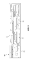
- FIG. 3 shows a schematic of an ex-situ doped semiconductor charge transport layer containing semiconductor and dopant material nanoparticles
- FIG. 4 gives the emission spectrum of an unpurified ZnTe quantum dot crude solution with excitation at 430 nm.
- FIG. 5 gives the IV response for a two-point probe measurement of film resistance of Cu-doped ZnTe.
- a typical colloidal inorganic nanoparticle 205 is shown in FIG. 2 .
- the inorganic nanoparticle 205 is composed of a semiconductor core 200 , on whose surface is bonded organic ligands 210 .
- the organic ligands 210 give stability to the resulting colloidal dispersion (the inorganic nanoparticle 205 and an appropriate solvent).
- the inorganic nanoparticle 205 shown in FIG. 2 is spherical in shape, nanoparticles can be synthesized to be shapes ranging from quantum rods and wires, to tetrapods and other multiply connected nanoparticles that show quantum confinement effects.
- Semiconductor films can be doped by a number of ways. Some of these are extrinsic processes, namely, the doping occurs after the materials comprising the layer have been grown or synthesized.
- extrinsic donors and acceptors can be introduced into a layer by ion implantation and by diffusion processes (P. J. George et al., Appl. Phys. Lett. 66, 3624 (1995)).
- the source for the dopant materials can be a solid source (metal film on the layer surface), a liquid source (containing appropriate metal ions), and a vapor source (e.g., closed tube diffusions containing a subliming metallic source).
- Adapting in-situ doping to inorganic nanoparticles 205 has a number of challenging issues associated with it. Foremost is the problem that doping levels are typically in the 1 part in 10 4 -10 5 range, while a 4 nm spherical nanoparticle only contains on the order of 1000 atoms (C. B. Murray et al., JACS 115, 8706 (1993)). As a result, many of the nanoparticles would not contain a dopant atom. This situation causes problems since if a large fraction of the nanoparticles are undoped, then these nanoparticles would be highly resistive which would result in the device layer being highly resistive.
- dopant material nanoparticles 320 are formed and co-dispersed with semiconductor nanoparticles 310 such that the diffusion source for dopant material atoms 340 is internal to the semiconductor transport layer 330 .
- each dopant material nanoparticle 320 inside of the semiconductor transport layer 330 acts as an internal source of dopant material atoms 340 .
- Two sets of anneals are performed on the semiconductor transport layer 330 containing semiconductor 310 and dopant material 320 nanoparticles.
- a lower temperature anneal (below 220° C.) is used to boil off the insulating organic ligands 210 .
- a higher temperature anneal (between 250 and 500° C.) is used to fuse the semiconductor nanoparticles 310 , resulting in a continuous semiconductor layer, and simultaneously causes the dopant material atoms 340 to diffuse out from the dopant material nanoparticles 320 and into the continuous semiconductor layer to provide appropriate doping so that an ex-situ doped semiconductor transport layer 300 is formed.
- Having an internal source for the dopant material atoms 340 has a few advantages over conventional methods: 1) A separate anneal step is not required in order diffuse the dopants, since it occurs during the fusing of the semiconductor nanoparticles; 2) Extra and costly processing steps are not required to deposit the diffusion source and remove it once the anneal has occurred; and 3) Diffusion occurs more rapidly and at lower temperatures since the diffusion sources are nanoparticles, the semiconductor matrix is initially porous (becomes less so during the fusing process), and the diffusion sources are distributed throughout the semiconductor matrix (less distance to travel). Even though FIG.
- FIG. 3 shows the shape of the semiconductor nanoparticles 310 to be a quantum wire, it could be any colloidal nanoparticle that shows quantum size effects, such as, quantum dots, quantum rods, branched quantum rods, tetrapods, and any other multiply connected nanoparticle that show quantum confinement effects.
- FIG. 3 shows the dopant material nanoparticle 320 to be a quantum dot, whereas, it can also be any colloidal nanoparticle, either singly or multiply connected, that shows quantum size effects.
- the semiconductor nanoparticles composing the ex-situ doped semiconductor transport layer 300 can be selected from type II-VI, III-V, IV-VI, or IV semiconductor materials.
- Specific type IV semiconductors are Si, Ge, and Sn.
- Specific type III-V semiconductors are AlN, AlP, AlAs, and AlSb; GaN, GaP, GaAs, and GaSb; and InN, InP, InAs, and InSb.
- Specific II-VI semiconductors are ZnS, ZnSe, and ZnTe; CdS, CdSe, and CdTe, HgS, HgSe, and HgTe.
- Specific IV-VI semiconductors are PbS, PbSe, and PbTe.
- dopant material atom 340 selection is limited by the requirement that one can synthesize a nanoparticle composed either solely of those atoms or shelled by these atoms. Accordingly, the common list of donors and acceptors gets slightly reduced to include only those elements whose state of matter at room temperature is either a metal or a semiconductor. Given this restriction, the type II-VI, III-V, IV-VI, and IV semiconductor materials can be doped by the invented ex-situ doping processes using the following list of dopant material atoms 340 .
- the dopant material atoms 340 can be selected from group III or V materials.
- the dopant material atoms 340 can be selected from group IIa, IIb, IV, or VI materials.
- the dopant material atoms 340 can be selected from group Ia, Ib, III, or V materials.
- the dopant material atoms 340 can be selected from group III or V materials. As can be seen from this list, group VII dopants have been excluded since they are gases at room temperature.
- Colloidal semiconductor nanoparticles 310 are made by chemical methods well known in the art. Typical synthetic routes are decomposition of molecular precursors at high temperatures in coordinating solvents (C. B. Murray et al., Annu. Rev. Mater. Sci. 30, 545 (2000)), solvothermal methods (O. Masala and R. Seshadri, Annu. Rev. Mater. Res. 34, 41 (2004)) and arrested precipitation (R. Rossetti et al., J. Chem. Phys. 80, 4464 (1984)). If, for example, the semiconductor nanoparticles 310 were CdSe quantum wires, then the following procedure yields both quantum wires and pre-wire aggregates (N.
- the cadmium precursor is cadmium acetate and the Se precursor is selenourea, where equal molar (1.27 ⁇ 10 ⁇ 4 moles) amounts are used in the synthesis.
- the coordinating solvent for the growth is octylamine (OA).
- OA octylamine
- the selenourea solution is placed in a syringe and injected into the 3-neck flask at 120° C.
- the contents of the flask turn a deep red within seconds of the injection.
- Under slow stirring the growth of CdSe quantum wires is continued for 4-6 hours at 120° C., followed by a final 20 minute anneal at 140° C.
- the colloidal dopant material nanoparticles 320 are also made by chemical methods well known in the art.
- the dopants can either be metal atoms (such as, Mg, Cu, Zn, or In) or semiconductor atoms (such as, Si, Ge, or Te).
- metal atoms such as, Mg, Cu, Zn, or In
- semiconductor atoms such as, Si, Ge, or Te.
- Colloidal synthesis of metallic nanoparticles of Au, Ag, and Cu and semiconductor nanoparticles of Si and Ge were reviewed by Masala et al. (O. Masala and R. Seshadri, Annu. Rev. Mater. Res. 34, 41 (2004)).
- Colloidal synthesis of Al nanoparticles was discussed by Jouet at al. (R. J. Jouet et al., Chem. Mater. 17, 2987 (2005)).
- the semiconductor nanoparticles 310 and the dopant material nanoparticles 320 it is then necessary to form a mixed dispersion of them and deposit the dispersion on a surface to form the ex-situ doped semiconductor transport layer 300 .
- Typical dopant concentrations in semiconductors are in the 1 part in 10 4 to 10 6 range.
- the ratio of dopant material atoms 340 to semiconductor atoms in the mixed dispersion is usually much greater than the 1 part in 10 4 to 10 6 range, with the range being as high as 1 part in 10 3 to 10 2 at times. In practice the proper ratio for achieving particular dopant (conductivity results for the transport layer) activation needs to be determined by experimentation.
- nanoparticle films As is well known in the art, three low cost techniques for forming nanoparticle films are depositing the colloidal mixed dispersion of semiconductor 310 and dopant material nanoparticles 320 by drop casting, spin coating and inkjetting.
- Common solvents for drop casting the mixed dispersion of semiconductor nanoparticles 310 and dopant material 320 nanoparticles are a 9:1 mixture of hexane:octane (C. B. Murray et al., Annu. Rev. Mater. Sci. 30, 545 (2000)).
- the organic ligands 210 that passivate the surfaces of the nanoparticles need to be chosen such that the semiconductor nanoparticles 310 and dopant material nanoparticles 320 are soluble in non-polar solvents.
- organic ligands with hydrocarbon-based tails are good choices, such as, the alkylamines.
- the ligands coming from the growth procedure can be exchanged for the organic ligand 210 of choice (C. B. Murray et al., Annu. Rev. Mater. Sci. 30, 545 (2000)).
- the requirements of the solvents are that they easily spread on the deposition surface and the solvents evaporate at a moderate rate during the spinning process.
- alcohol-based polar solvents are a good choice; for example, combining a low boiling point alcohol, such as, ethanol, with higher boiling point alcohols, such as, a butanol-hexanol mixture or 1-propanol, results in good film formation.
- ligand exchange can be used to attach an organic ligand 210 (to the semiconductor nanoparticles 310 and dopant material nanoparticles 320 ) whose tail is soluble in polar solvents; pyridine is an example of a suitable ligand.
- the semiconductor transport layer 330 is subjected to two sets of anneals.
- the first anneal is performed in order to remove the insulating organic ligands 210 from the surfaces of the nanoparticles.
- the annealing can take place in either a tube furnace or a rapid thermal annealer, under either a vacuum or with an inert gas overpressure. As is well known in the art, other heating apparatus can also be used to boil off the organic ligands 210 . Without the first annealing step, the resulting ex-situ doped semiconductor transport layers 300 would be highly resistive.
- the organic ligands 210 By choosing the organic ligands 210 to have a low boiling point (less than 200° C.), they can be made to evaporate from the film during an annealing process (C. B. Murray et al., Annu. Rev. Mater. Sci. 30, 545 (2000)) where the anneal temperature is below 220° C. Consequently, for films formed by drop casting with non-polar solvents, shorter chained primary amines, such as, hexylamine are preferred; for films formed by spin coating with polar solvents, pyridine is a preferred ligand.
- a second anneal step is performed to fuse the semiconductor nanoparticles and form a continuous semiconductor layer; while, simultaneously causing the dopant material atoms 340 to diffuse out from the dopant material nanoparticles 320 and into the continuous semiconductor layer to provide appropriate doping so that an ex-situ doped semiconductor transport layer 300 is formed.
- the ex-situ doped semiconductor transport layer 300 remains resistive since there is poor connectivity between the semiconductor nanoparticles 310 and electron and holes can get trapped by the semiconductor nanoparticle's 310 surface states.
- the fusing process can be performed at moderate temperatures since nanoparticles melt at much reduced temperatures compared to their bulk counterparts (A. N. Goldstein et al., Science 256, 1425 (1992)). Consequently, it is desirable that the semiconductor nanoparticles 310 have diameters less than 5 nm in order to enhance the sintering process, with a preferred size of 1-3 nm.
- Typical annealing temperatures are between 250 and 500° C. The annealing can take place in either a tube furnace or a rapid thermal annealer, where a variety of gases (such as, nitrogen, argon, oxygen, hydrogen, or forming gas) can be used depending on the desired outcome.
- Doped and undoped semiconductor transport layers were formed on glass substrates.
- the test system was ZnTe, with and without Cu doping (an acceptor for ZnTe which substitutes on the cation site).
- Undoped ZnTe semiconductor nanoparticles 310 were synthesized by adapting the procedures commonly used to form ZnSe spherical dots (M. A. Hines et al., J. Phys. Chem. B102, 3655 (1998)). More specifically, 4 g of dried and degassed hexadecylamine (HDA) was placed in a three-neck flask and heated, under argon, to 290° C. on a Schlenk line.
- HDA dried and degassed hexadecylamine
- Te precursor a 0.25 M solution (called TOPTe) of Te in trioctylphosphine (TOP) was formed by heating under vacuum a mixture of Te powder and TOP at 190° C., while vigorously stirring for ⁇ 3-4 hours. The resulting solution was clear and has a green-yellow appearance.
- a syringe was filled with 0.4 mmol of diethylzinc (from a 1 M diethylzinc in hexane solution), 1.6 mmol of TOPTe, and 2.0 ml of additional TOP. The syringe contents were quickly injected into the three-neck flask, while the solution was vigorously stirred.
- the reaction temperature immediately fell ⁇ 25° C. It was maintained at 265° C. for 10 minutes in order to form orange-red emitting ZnTe nanocrystals (viewable in room lights).
- the fluorescence spectrum of the ZnTe crude solution is given in FIG. 4 .
- the UV-VIS absorption spectrum of the ZnTe quantum dot crude solution shows that the dots have a distinct room temperature first exciton absorption peak at ⁇ 430 nm.
- the UV-VIS absorption spectrum of the copper crude solution showed the copper nanoparticle plasmon peak to be at ⁇ 565 nm, in agreement with the results of Hambrock et al. (J. Hambrock et al., Chem. Commun. 68 (2002)).
- TEMs indicated that the copper nanoparticles were spherical with particle diameters ranging between 6 and 12 nm.
- the ohmic metals (in deposition order) consisted of 150 nm of Pd (sputtered) and 300 nm of Ag (thermally evaporated). Palladium is a well-known ohmic contact for ZnTe, while the Ag was deposited in order to aid in probing the ohmic contacts. Prior to metal evaporation, the films were cleaned with acetone, methanol, and water, and then blown dry with nitrogen. The contacts were annealed in a tube furnace under flowing argon for 5 minutes at 240° C. For all of the annealing and contact formation steps, the doped and undoped samples were processed simultaneously.
- FIG. 5 shows the IV characteristics of a two-point probe measurement made for the doped sample.
Abstract
Description
- 100 substrate
- 105 light emitting diode device
- 110 p-contact layer
- 120 p-transport layer
- 130 intrinsic emitter layer
- 140 n-transport layer
- 150 n-contact layer
- 160 anode
- 170 cathode
- 200 semiconductor core
- 205 inorganic nanoparticle
- 210 organic ligand
- 300 ex-situ doped semiconductor transport layer
- 310 semiconductor nanoparticles
- 320 dopant material nanoparticle
- 330 semiconductor transport layer
- 340 dopant material atoms
Claims (17)
Priority Applications (6)
| Application Number | Priority Date | Filing Date | Title |
|---|---|---|---|
| US11/677,794 US7375011B1 (en) | 2007-02-22 | 2007-02-22 | Ex-situ doped semiconductor transport layer |
| PCT/US2007/025211 WO2008103161A1 (en) | 2007-02-22 | 2007-12-10 | Ex-situ doped semiconductor transport layer |
| CN2007800515631A CN101611480B (en) | 2007-02-22 | 2007-12-10 | Method for manufacturing Ex-situ doped semiconductor transport layer |
| JP2009550856A JP5171848B2 (en) | 2007-02-22 | 2007-12-10 | Ex situ doped nanoparticle semiconductor transport layer |
| EP07862703A EP2122673B1 (en) | 2007-02-22 | 2007-12-10 | Ex-situ doped semiconductor transport layer |
| TW096149078A TWI411016B (en) | 2007-02-22 | 2007-12-20 | Ex-situ doped semiconductor transport layer |
Applications Claiming Priority (1)
| Application Number | Priority Date | Filing Date | Title |
|---|---|---|---|
| US11/677,794 US7375011B1 (en) | 2007-02-22 | 2007-02-22 | Ex-situ doped semiconductor transport layer |
Publications (1)
| Publication Number | Publication Date |
|---|---|
| US7375011B1 true US7375011B1 (en) | 2008-05-20 |
Family
ID=39370788
Family Applications (1)
| Application Number | Title | Priority Date | Filing Date |
|---|---|---|---|
| US11/677,794 Expired - Fee Related US7375011B1 (en) | 2007-02-22 | 2007-02-22 | Ex-situ doped semiconductor transport layer |
Country Status (6)
| Country | Link |
|---|---|
| US (1) | US7375011B1 (en) |
| EP (1) | EP2122673B1 (en) |
| JP (1) | JP5171848B2 (en) |
| CN (1) | CN101611480B (en) |
| TW (1) | TWI411016B (en) |
| WO (1) | WO2008103161A1 (en) |
Cited By (7)
| Publication number | Priority date | Publication date | Assignee | Title |
|---|---|---|---|---|
| US20080152938A1 (en) * | 2006-12-21 | 2008-06-26 | Maxim Kelman | Group iv nanoparticles and films thereof |
| US20080156371A1 (en) * | 2006-12-11 | 2008-07-03 | Locascio Michael | Nanostructured layers, method of making nanostructured layers, and application thereof |
| US20090014423A1 (en) * | 2007-07-10 | 2009-01-15 | Xuegeng Li | Concentric flow-through plasma reactor and methods therefor |
| US20090044661A1 (en) * | 2007-07-10 | 2009-02-19 | Xuegeng Li | Methods and apparatus for the production of group iv nanoparticles in a flow-through plasma reactor |
| US20090053878A1 (en) * | 2007-08-21 | 2009-02-26 | Maxim Kelman | Method for fabrication of semiconductor thin films using flash lamp processing |
| US20090255222A1 (en) * | 2007-07-10 | 2009-10-15 | Raul Cortez | Methods and apparatus for the in situ collection of nucleated particles |
| US20150072460A1 (en) * | 2010-02-23 | 2015-03-12 | Saint-Gobain Glass France | Device and method for precipitating a layer on a substrate |
Families Citing this family (2)
| Publication number | Priority date | Publication date | Assignee | Title |
|---|---|---|---|---|
| GB2461079A (en) | 2008-06-19 | 2009-12-23 | Mighton Products Ltd | Sash window restrictor having a protruding member and retaining mechanism |
| TWI702405B (en) * | 2019-08-12 | 2020-08-21 | 久盛光電股份有限公司 | Photosensitive thin film transistor and electromagnetic wave detection device |
Citations (2)
| Publication number | Priority date | Publication date | Assignee | Title |
|---|---|---|---|---|
| US5262357A (en) * | 1991-11-22 | 1993-11-16 | The Regents Of The University Of California | Low temperature thin films formed from nanocrystal precursors |
| US7087832B2 (en) | 2002-09-05 | 2006-08-08 | Nanosys, Inc. | Nanostructure and nanocomposite based compositions and photovoltaic devices |
Family Cites Families (5)
| Publication number | Priority date | Publication date | Assignee | Title |
|---|---|---|---|---|
| GB0225202D0 (en) * | 2002-10-30 | 2002-12-11 | Hewlett Packard Co | Electronic components |
| US7879696B2 (en) * | 2003-07-08 | 2011-02-01 | Kovio, Inc. | Compositions and methods for forming a semiconducting and/or silicon-containing film, and structures formed therefrom |
| GB0409877D0 (en) * | 2004-04-30 | 2004-06-09 | Univ Manchester | Preparation of nanoparticle materials |
| US7507618B2 (en) * | 2005-06-27 | 2009-03-24 | 3M Innovative Properties Company | Method for making electronic devices using metal oxide nanoparticles |
| CN100387101C (en) * | 2005-07-01 | 2008-05-07 | 中山大学 | Method for improving organic electro-luminescence device lifetime |
-
2007
- 2007-02-22 US US11/677,794 patent/US7375011B1/en not_active Expired - Fee Related
- 2007-12-10 WO PCT/US2007/025211 patent/WO2008103161A1/en active Application Filing
- 2007-12-10 EP EP07862703A patent/EP2122673B1/en not_active Not-in-force
- 2007-12-10 JP JP2009550856A patent/JP5171848B2/en not_active Expired - Fee Related
- 2007-12-10 CN CN2007800515631A patent/CN101611480B/en not_active Expired - Fee Related
- 2007-12-20 TW TW096149078A patent/TWI411016B/en not_active IP Right Cessation
Patent Citations (2)
| Publication number | Priority date | Publication date | Assignee | Title |
|---|---|---|---|---|
| US5262357A (en) * | 1991-11-22 | 1993-11-16 | The Regents Of The University Of California | Low temperature thin films formed from nanocrystal precursors |
| US7087832B2 (en) | 2002-09-05 | 2006-08-08 | Nanosys, Inc. | Nanostructure and nanocomposite based compositions and photovoltaic devices |
Non-Patent Citations (18)
| Title |
|---|
| A. N. Goldstein et al., Melting in Semiconductor Nanocrystals, Science 256, 1425-1426 (1992). |
| C. B. Murray et al., Synthesis and Characterization of Monodisperse Nanocrystals and Close-Packed Nanocrystal Assemblies, Annu. Rev. Mater. Sci. 30, 545-593 (2000). |
| Dhere et al, Thin-film photovoltaics, J. Vac. Sci. Tech. A23(4) Jul./Aug. 2005, pp. 1208-1214. |
| Erwin et al, Doping semiconductor nanocrystals, Nature Letters, V43617, Jul. 2005, pp. 91-94. |
| Gur et al, Air Stable All Inorganic Nanocrystal Solar Cells Processed From Solution, Science, Vo. 310, Oct. 2005, 462-465. |
| Hambrock et al, A non-aqueous organometallic route to highly monodispersed copper nanoparticles using [Cu(OCHChMe)CH<SUB>2</SUB>NMe<SUB>2</SUB>)<SUB>2</SUB>], Chem. Commun. pp. 68-69 (2002). |
| Huang et al, Low voltage organic electroluminescent devices using pin structures, App. Phys. Lett. V.80, No. 1, Jan. 2002, pp. 139-141. |
| JV Singh et al, Synthesis and Characterization of Some Alkoxide Derivatives of Copper (II), Z. anorg.allg.Chem, 477 pp. 235-240 (1981). |
| K. B. Kahen, Rigorous optical modeling of multilayer organic light-emitting diode devices, Appl. Phys. Lett. 78, 1649-1651 (2001). |
| Liu et al, Employing End-Functional Polythiophene to Control the Morphology of Nanocrystal-Polymer Composites in Hybrid Solar Cells, J. Am. Chem. Soc. 2004, 126, pp. 6550-6551. |
| M. A. Hines et al, Bright UV-Blue Luminescent Colloidal ZnSe Nanocrystals, J. Phys. Chem. B102 pp. 3655-3657 (1998). |
| Murray et al, Synthesis and Characterization of Nearly Monodisperse CdE (E=S, Se, Te) Semiconductor Nanocrystallites, J. Am Chem, 1993, 115 pp. 8706-8715. |
| O. Masala et al, Synthesis Routes for Large Volumes of Nanoparticles, Annu. Rev. Mater. Res. 34, (2004) pp. 41-81. |
| P. J. George et al., Doping of chemically deposited intrinsic CdS thin films to n type by thermal diffusion of indium, Appl. Phys. Lett. 66, 3624-3626 [1995]. |
| Pradham et al, Collodial CdSe Quantum Wires by Oriented Attachment, Nano Letters, V01. 6, No. 4, pp. 720-724, 2006. |
| R. J. Jouet et al, Surface Passivation of Bare Aluminum Nanoparticles Using Perfluoroalkyl Carboxylic Acids, Chem. Mater. 17, pp. 2987-2996 (2005). |
| Rossetti et al, Size effects in the excited electronic states of small colloidal CdsS crystallites, J. Chem Phys, Vo. 80, No. 9, May 1, 1984, pp. 4464-4469. |
| Yu et al n-Type Conducting CdSe Nanocrystal Solids, Science, vol. 300, Mayh 2003, pp. 1277-1280. |
Cited By (14)
| Publication number | Priority date | Publication date | Assignee | Title |
|---|---|---|---|---|
| US7785657B2 (en) * | 2006-12-11 | 2010-08-31 | Evident Technologies, Inc. | Nanostructured layers, method of making nanostructured layers, and application thereof |
| US20080156371A1 (en) * | 2006-12-11 | 2008-07-03 | Locascio Michael | Nanostructured layers, method of making nanostructured layers, and application thereof |
| US8368048B2 (en) | 2006-12-11 | 2013-02-05 | Nanoco Technologies, Ltd. | Nanostructured layers, methods of making nanostructured layers, and application thereof |
| US20100270511A1 (en) * | 2006-12-11 | 2010-10-28 | Locascio Michael | Nanostructured layers, methods of making nanostructured layers, and application thereof |
| US7718707B2 (en) | 2006-12-21 | 2010-05-18 | Innovalight, Inc. | Method for preparing nanoparticle thin films |
| US20080152938A1 (en) * | 2006-12-21 | 2008-06-26 | Maxim Kelman | Group iv nanoparticles and films thereof |
| US20090255222A1 (en) * | 2007-07-10 | 2009-10-15 | Raul Cortez | Methods and apparatus for the in situ collection of nucleated particles |
| US20090044661A1 (en) * | 2007-07-10 | 2009-02-19 | Xuegeng Li | Methods and apparatus for the production of group iv nanoparticles in a flow-through plasma reactor |
| US20090014423A1 (en) * | 2007-07-10 | 2009-01-15 | Xuegeng Li | Concentric flow-through plasma reactor and methods therefor |
| US8471170B2 (en) | 2007-07-10 | 2013-06-25 | Innovalight, Inc. | Methods and apparatus for the production of group IV nanoparticles in a flow-through plasma reactor |
| US8968438B2 (en) | 2007-07-10 | 2015-03-03 | Innovalight, Inc. | Methods and apparatus for the in situ collection of nucleated particles |
| US20090053878A1 (en) * | 2007-08-21 | 2009-02-26 | Maxim Kelman | Method for fabrication of semiconductor thin films using flash lamp processing |
| US20150072460A1 (en) * | 2010-02-23 | 2015-03-12 | Saint-Gobain Glass France | Device and method for precipitating a layer on a substrate |
| US9343610B2 (en) * | 2010-02-23 | 2016-05-17 | Saint-Gobain Glass France | Device and method for precipitating a layer on a substrate |
Also Published As
| Publication number | Publication date |
|---|---|
| TW200845149A (en) | 2008-11-16 |
| EP2122673B1 (en) | 2013-02-13 |
| WO2008103161A1 (en) | 2008-08-28 |
| TWI411016B (en) | 2013-10-01 |
| CN101611480B (en) | 2012-09-05 |
| JP2010519765A (en) | 2010-06-03 |
| EP2122673A1 (en) | 2009-11-25 |
| CN101611480A (en) | 2009-12-23 |
| JP5171848B2 (en) | 2013-03-27 |
Similar Documents
| Publication | Publication Date | Title |
|---|---|---|
| US7605062B2 (en) | Doped nanoparticle-based semiconductor junction | |
| EP2122673B1 (en) | Ex-situ doped semiconductor transport layer | |
| US7494903B2 (en) | Doped nanoparticle semiconductor charge transport layer | |
| US7615800B2 (en) | Quantum dot light emitting layer | |
| CN100361320C (en) | Zinc oxide films containing P-type dopant and process for preparing same | |
| US20110240099A1 (en) | Photovoltaic nanowire device | |
| Su et al. | Homogeneous ZnO nanowire arrays pn junction for blue light-emitting diode applications | |
| US20110073835A1 (en) | Semiconductor nanocrystal film | |
| TW200541070A (en) | Semiconductor material and semiconductor element using the same | |
| Yatskiv et al. | Electrical and optical properties of rectifying ZnO homojunctions fabricated by wet chemistry methods | |
| Abdel-Salam et al. | Anisotropic CuInSe2 nanocrystals: synthesis, optical properties and their effect on photoelectric response of dye-sensitized solar cell | |
| US20110076839A1 (en) | Making films composed of semiconductor nanocrystals | |
| Kim et al. | Impact of Sb incorporation on MOVPE-grown “bulk” InGaAs (Sb) N films for solar cell application | |
| Mock et al. | Vacancy doping and charge transport in B i 2 S 3 nanoparticle films for photovoltaic applications | |
| Wang et al. | Manipulating Depletion Region of Aqueous‐Processed Nanocrystals Solar Cells with Widened Fermi Level Offset | |
| US20130126892A1 (en) | P-Type Amorphous GaNAs Alloy as Low Resistant Ohmic Contact to P-Type Group III-Nitride Semiconductors | |
| Tietjen et al. | The Preparation and Properties of Vapor‐Deposited Epitaxial InAs1− x P x Using Arsine and Phosphine | |
| Bastola | CdTe Back Contact Engineering via Nanomaterials, Chemical Etching, Doping, and Surface Passivation | |
| Ikeda et al. | III–V–N Materials for Super-High Efficiency Multi Junction Solar Cells | |
| Hayashida et al. | Growth of n-type ZnTe films and formation of ohmic contacts | |
| Johnston et al. | Thin film AlAs/GaAs on graphite solar cells | |
| Athavan | Fundamental Properties of Functional Zinc Oxide Nanowires Obtained by Electrochemical Method and Their Device Applications |
Legal Events
| Date | Code | Title | Description |
|---|---|---|---|
| AS | Assignment |
Owner name: EASTMAN KODAK COMPANY, NEW YORK Free format text: ASSIGNMENT OF ASSIGNORS INTEREST;ASSIGNOR:KAHEN, KEITH B.;REEL/FRAME:018921/0548 Effective date: 20070222 |
|
| STCF | Information on status: patent grant |
Free format text: PATENTED CASE |
|
| CC | Certificate of correction | ||
| FPAY | Fee payment |
Year of fee payment: 4 |
|
| AS | Assignment |
Owner name: CITICORP NORTH AMERICA, INC., AS AGENT, NEW YORK Free format text: SECURITY INTEREST;ASSIGNORS:EASTMAN KODAK COMPANY;PAKON, INC.;REEL/FRAME:028201/0420 Effective date: 20120215 |
|
| AS | Assignment |
Owner name: WILMINGTON TRUST, NATIONAL ASSOCIATION, AS AGENT, Free format text: PATENT SECURITY AGREEMENT;ASSIGNORS:EASTMAN KODAK COMPANY;PAKON, INC.;REEL/FRAME:030122/0235 Effective date: 20130322 Owner name: WILMINGTON TRUST, NATIONAL ASSOCIATION, AS AGENT, MINNESOTA Free format text: PATENT SECURITY AGREEMENT;ASSIGNORS:EASTMAN KODAK COMPANY;PAKON, INC.;REEL/FRAME:030122/0235 Effective date: 20130322 |
|
| AS | Assignment |
Owner name: JPMORGAN CHASE BANK, N.A., AS ADMINISTRATIVE, DELAWARE Free format text: INTELLECTUAL PROPERTY SECURITY AGREEMENT (FIRST LIEN);ASSIGNORS:EASTMAN KODAK COMPANY;FAR EAST DEVELOPMENT LTD.;FPC INC.;AND OTHERS;REEL/FRAME:031158/0001 Effective date: 20130903 Owner name: BARCLAYS BANK PLC, AS ADMINISTRATIVE AGENT, NEW YORK Free format text: INTELLECTUAL PROPERTY SECURITY AGREEMENT (SECOND LIEN);ASSIGNORS:EASTMAN KODAK COMPANY;FAR EAST DEVELOPMENT LTD.;FPC INC.;AND OTHERS;REEL/FRAME:031159/0001 Effective date: 20130903 Owner name: BANK OF AMERICA N.A., AS AGENT, MASSACHUSETTS Free format text: INTELLECTUAL PROPERTY SECURITY AGREEMENT (ABL);ASSIGNORS:EASTMAN KODAK COMPANY;FAR EAST DEVELOPMENT LTD.;FPC INC.;AND OTHERS;REEL/FRAME:031162/0117 Effective date: 20130903 Owner name: BARCLAYS BANK PLC, AS ADMINISTRATIVE AGENT, NEW YO Free format text: INTELLECTUAL PROPERTY SECURITY AGREEMENT (SECOND LIEN);ASSIGNORS:EASTMAN KODAK COMPANY;FAR EAST DEVELOPMENT LTD.;FPC INC.;AND OTHERS;REEL/FRAME:031159/0001 Effective date: 20130903 Owner name: PAKON, INC., NEW YORK Free format text: RELEASE OF SECURITY INTEREST IN PATENTS;ASSIGNORS:CITICORP NORTH AMERICA, INC., AS SENIOR DIP AGENT;WILMINGTON TRUST, NATIONAL ASSOCIATION, AS JUNIOR DIP AGENT;REEL/FRAME:031157/0451 Effective date: 20130903 Owner name: EASTMAN KODAK COMPANY, NEW YORK Free format text: RELEASE OF SECURITY INTEREST IN PATENTS;ASSIGNORS:CITICORP NORTH AMERICA, INC., AS SENIOR DIP AGENT;WILMINGTON TRUST, NATIONAL ASSOCIATION, AS JUNIOR DIP AGENT;REEL/FRAME:031157/0451 Effective date: 20130903 Owner name: JPMORGAN CHASE BANK, N.A., AS ADMINISTRATIVE, DELA Free format text: INTELLECTUAL PROPERTY SECURITY AGREEMENT (FIRST LIEN);ASSIGNORS:EASTMAN KODAK COMPANY;FAR EAST DEVELOPMENT LTD.;FPC INC.;AND OTHERS;REEL/FRAME:031158/0001 Effective date: 20130903 |
|
| FPAY | Fee payment |
Year of fee payment: 8 |
|
| AS | Assignment |
Owner name: EASTMAN KODAK COMPANY, NEW YORK Free format text: RELEASE BY SECURED PARTY;ASSIGNOR:BANK OF AMERICA, N.A.;REEL/FRAME:041144/0090 Effective date: 20170126 Owner name: EASTMAN KODAK COMPANY, NEW YORK Free format text: RELEASE BY SECURED PARTY;ASSIGNOR:JP MORGAN CHASE BANK N.A.;REEL/FRAME:041144/0005 Effective date: 20170126 |
|
| AS | Assignment |
Owner name: NANOCO TECHNOLOGIES LIMITED, UNITED KINGDOM Free format text: ASSIGNMENT OF ASSIGNORS INTEREST;ASSIGNOR:EASTMAN KODAK COMPANY;REEL/FRAME:045143/0757 Effective date: 20161213 |
|
| AS | Assignment |
Owner name: KODAK PORTUGUESA LIMITED, NEW YORK Free format text: RELEASE BY SECURED PARTY;ASSIGNOR:JP MORGAN CHASE BANK, N.A., AS ADMINISTRATIVE AGENT;REEL/FRAME:050239/0001 Effective date: 20190617 Owner name: KODAK (NEAR EAST), INC., NEW YORK Free format text: RELEASE BY SECURED PARTY;ASSIGNOR:JP MORGAN CHASE BANK, N.A., AS ADMINISTRATIVE AGENT;REEL/FRAME:050239/0001 Effective date: 20190617 Owner name: FAR EAST DEVELOPMENT LTD., NEW YORK Free format text: RELEASE BY SECURED PARTY;ASSIGNOR:JP MORGAN CHASE BANK, N.A., AS ADMINISTRATIVE AGENT;REEL/FRAME:050239/0001 Effective date: 20190617 Owner name: KODAK REALTY, INC., NEW YORK Free format text: RELEASE BY SECURED PARTY;ASSIGNOR:JP MORGAN CHASE BANK, N.A., AS ADMINISTRATIVE AGENT;REEL/FRAME:050239/0001 Effective date: 20190617 Owner name: PAKON, INC., NEW YORK Free format text: RELEASE BY SECURED PARTY;ASSIGNOR:JP MORGAN CHASE BANK, N.A., AS ADMINISTRATIVE AGENT;REEL/FRAME:050239/0001 Effective date: 20190617 Owner name: KODAK AMERICAS, LTD., NEW YORK Free format text: RELEASE BY SECURED PARTY;ASSIGNOR:JP MORGAN CHASE BANK, N.A., AS ADMINISTRATIVE AGENT;REEL/FRAME:050239/0001 Effective date: 20190617 Owner name: CREO MANUFACTURING AMERICA LLC, NEW YORK Free format text: RELEASE BY SECURED PARTY;ASSIGNOR:JP MORGAN CHASE BANK, N.A., AS ADMINISTRATIVE AGENT;REEL/FRAME:050239/0001 Effective date: 20190617 Owner name: EASTMAN KODAK COMPANY, NEW YORK Free format text: RELEASE BY SECURED PARTY;ASSIGNOR:JP MORGAN CHASE BANK, N.A., AS ADMINISTRATIVE AGENT;REEL/FRAME:050239/0001 Effective date: 20190617 Owner name: KODAK PHILIPPINES, LTD., NEW YORK Free format text: RELEASE BY SECURED PARTY;ASSIGNOR:JP MORGAN CHASE BANK, N.A., AS ADMINISTRATIVE AGENT;REEL/FRAME:050239/0001 Effective date: 20190617 Owner name: LASER PACIFIC MEDIA CORPORATION, NEW YORK Free format text: RELEASE BY SECURED PARTY;ASSIGNOR:JP MORGAN CHASE BANK, N.A., AS ADMINISTRATIVE AGENT;REEL/FRAME:050239/0001 Effective date: 20190617 Owner name: FPC, INC., NEW YORK Free format text: RELEASE BY SECURED PARTY;ASSIGNOR:JP MORGAN CHASE BANK, N.A., AS ADMINISTRATIVE AGENT;REEL/FRAME:050239/0001 Effective date: 20190617 Owner name: QUALEX, INC., NEW YORK Free format text: RELEASE BY SECURED PARTY;ASSIGNOR:JP MORGAN CHASE BANK, N.A., AS ADMINISTRATIVE AGENT;REEL/FRAME:050239/0001 Effective date: 20190617 Owner name: NPEC, INC., NEW YORK Free format text: RELEASE BY SECURED PARTY;ASSIGNOR:JP MORGAN CHASE BANK, N.A., AS ADMINISTRATIVE AGENT;REEL/FRAME:050239/0001 Effective date: 20190617 Owner name: KODAK IMAGING NETWORK, INC., NEW YORK Free format text: RELEASE BY SECURED PARTY;ASSIGNOR:JP MORGAN CHASE BANK, N.A., AS ADMINISTRATIVE AGENT;REEL/FRAME:050239/0001 Effective date: 20190617 Owner name: KODAK AVIATION LEASING LLC, NEW YORK Free format text: RELEASE BY SECURED PARTY;ASSIGNOR:JP MORGAN CHASE BANK, N.A., AS ADMINISTRATIVE AGENT;REEL/FRAME:050239/0001 Effective date: 20190617 |
|
| AS | Assignment |
Owner name: EASTMAN KODAK COMPANY, NEW YORK Free format text: RELEASE BY SECURED PARTY;ASSIGNOR:JP MORGAN CHASE BANK, N.A., AS ADMINISTRATIVE AGENT;REEL/FRAME:049901/0001 Effective date: 20190617 Owner name: CREO MANUFACTURING AMERICA LLC, NEW YORK Free format text: RELEASE BY SECURED PARTY;ASSIGNOR:JP MORGAN CHASE BANK, N.A., AS ADMINISTRATIVE AGENT;REEL/FRAME:049901/0001 Effective date: 20190617 Owner name: KODAK AMERICAS, LTD., NEW YORK Free format text: RELEASE BY SECURED PARTY;ASSIGNOR:JP MORGAN CHASE BANK, N.A., AS ADMINISTRATIVE AGENT;REEL/FRAME:049901/0001 Effective date: 20190617 Owner name: KODAK REALTY, INC., NEW YORK Free format text: RELEASE BY SECURED PARTY;ASSIGNOR:JP MORGAN CHASE BANK, N.A., AS ADMINISTRATIVE AGENT;REEL/FRAME:049901/0001 Effective date: 20190617 Owner name: KODAK IMAGING NETWORK, INC., NEW YORK Free format text: RELEASE BY SECURED PARTY;ASSIGNOR:JP MORGAN CHASE BANK, N.A., AS ADMINISTRATIVE AGENT;REEL/FRAME:049901/0001 Effective date: 20190617 Owner name: KODAK PHILIPPINES, LTD., NEW YORK Free format text: RELEASE BY SECURED PARTY;ASSIGNOR:JP MORGAN CHASE BANK, N.A., AS ADMINISTRATIVE AGENT;REEL/FRAME:049901/0001 Effective date: 20190617 Owner name: NPEC, INC., NEW YORK Free format text: RELEASE BY SECURED PARTY;ASSIGNOR:JP MORGAN CHASE BANK, N.A., AS ADMINISTRATIVE AGENT;REEL/FRAME:049901/0001 Effective date: 20190617 Owner name: LASER PACIFIC MEDIA CORPORATION, NEW YORK Free format text: RELEASE BY SECURED PARTY;ASSIGNOR:JP MORGAN CHASE BANK, N.A., AS ADMINISTRATIVE AGENT;REEL/FRAME:049901/0001 Effective date: 20190617 Owner name: PAKON, INC., NEW YORK Free format text: RELEASE BY SECURED PARTY;ASSIGNOR:JP MORGAN CHASE BANK, N.A., AS ADMINISTRATIVE AGENT;REEL/FRAME:049901/0001 Effective date: 20190617 Owner name: KODAK PORTUGUESA LIMITED, NEW YORK Free format text: RELEASE BY SECURED PARTY;ASSIGNOR:JP MORGAN CHASE BANK, N.A., AS ADMINISTRATIVE AGENT;REEL/FRAME:049901/0001 Effective date: 20190617 Owner name: QUALEX, INC., NEW YORK Free format text: RELEASE BY SECURED PARTY;ASSIGNOR:JP MORGAN CHASE BANK, N.A., AS ADMINISTRATIVE AGENT;REEL/FRAME:049901/0001 Effective date: 20190617 Owner name: KODAK AVIATION LEASING LLC, NEW YORK Free format text: RELEASE BY SECURED PARTY;ASSIGNOR:JP MORGAN CHASE BANK, N.A., AS ADMINISTRATIVE AGENT;REEL/FRAME:049901/0001 Effective date: 20190617 Owner name: FAR EAST DEVELOPMENT LTD., NEW YORK Free format text: RELEASE BY SECURED PARTY;ASSIGNOR:JP MORGAN CHASE BANK, N.A., AS ADMINISTRATIVE AGENT;REEL/FRAME:049901/0001 Effective date: 20190617 Owner name: PFC, INC., NEW YORK Free format text: RELEASE BY SECURED PARTY;ASSIGNOR:JP MORGAN CHASE BANK, N.A., AS ADMINISTRATIVE AGENT;REEL/FRAME:049901/0001 Effective date: 20190617 Owner name: KODAK (NEAR EAST), INC., NEW YORK Free format text: RELEASE BY SECURED PARTY;ASSIGNOR:JP MORGAN CHASE BANK, N.A., AS ADMINISTRATIVE AGENT;REEL/FRAME:049901/0001 Effective date: 20190617 |
|
| FEPP | Fee payment procedure |
Free format text: MAINTENANCE FEE REMINDER MAILED (ORIGINAL EVENT CODE: REM.); ENTITY STATUS OF PATENT OWNER: LARGE ENTITY |
|
| AS | Assignment |
Owner name: FPC INC., NEW YORK Free format text: RELEASE BY SECURED PARTY;ASSIGNOR:BARCLAYS BANK PLC;REEL/FRAME:052773/0001 Effective date: 20170202 Owner name: EASTMAN KODAK COMPANY, NEW YORK Free format text: RELEASE BY SECURED PARTY;ASSIGNOR:BARCLAYS BANK PLC;REEL/FRAME:052773/0001 Effective date: 20170202 Owner name: FAR EAST DEVELOPMENT LTD., NEW YORK Free format text: RELEASE BY SECURED PARTY;ASSIGNOR:BARCLAYS BANK PLC;REEL/FRAME:052773/0001 Effective date: 20170202 Owner name: LASER PACIFIC MEDIA CORPORATION, NEW YORK Free format text: RELEASE BY SECURED PARTY;ASSIGNOR:BARCLAYS BANK PLC;REEL/FRAME:052773/0001 Effective date: 20170202 Owner name: KODAK AMERICAS LTD., NEW YORK Free format text: RELEASE BY SECURED PARTY;ASSIGNOR:BARCLAYS BANK PLC;REEL/FRAME:052773/0001 Effective date: 20170202 Owner name: KODAK REALTY INC., NEW YORK Free format text: RELEASE BY SECURED PARTY;ASSIGNOR:BARCLAYS BANK PLC;REEL/FRAME:052773/0001 Effective date: 20170202 Owner name: NPEC INC., NEW YORK Free format text: RELEASE BY SECURED PARTY;ASSIGNOR:BARCLAYS BANK PLC;REEL/FRAME:052773/0001 Effective date: 20170202 Owner name: KODAK PHILIPPINES LTD., NEW YORK Free format text: RELEASE BY SECURED PARTY;ASSIGNOR:BARCLAYS BANK PLC;REEL/FRAME:052773/0001 Effective date: 20170202 Owner name: KODAK (NEAR EAST) INC., NEW YORK Free format text: RELEASE BY SECURED PARTY;ASSIGNOR:BARCLAYS BANK PLC;REEL/FRAME:052773/0001 Effective date: 20170202 Owner name: QUALEX INC., NEW YORK Free format text: RELEASE BY SECURED PARTY;ASSIGNOR:BARCLAYS BANK PLC;REEL/FRAME:052773/0001 Effective date: 20170202 |
|
| LAPS | Lapse for failure to pay maintenance fees |
Free format text: PATENT EXPIRED FOR FAILURE TO PAY MAINTENANCE FEES (ORIGINAL EVENT CODE: EXP.); ENTITY STATUS OF PATENT OWNER: LARGE ENTITY |
|
| STCH | Information on status: patent discontinuation |
Free format text: PATENT EXPIRED DUE TO NONPAYMENT OF MAINTENANCE FEES UNDER 37 CFR 1.362 |
|
| FP | Lapsed due to failure to pay maintenance fee |
Effective date: 20200520 |