US7395474B2 - Lab-on-chip system and method and apparatus for manufacturing and operating same - Google Patents
Lab-on-chip system and method and apparatus for manufacturing and operating same Download PDFInfo
- Publication number
- US7395474B2 US7395474B2 US10/909,920 US90992004A US7395474B2 US 7395474 B2 US7395474 B2 US 7395474B2 US 90992004 A US90992004 A US 90992004A US 7395474 B2 US7395474 B2 US 7395474B2
- Authority
- US
- United States
- Prior art keywords
- lab
- chip system
- electrical
- micro
- substrate
- Prior art date
- Legal status (The legal status is an assumption and is not a legal conclusion. Google has not performed a legal analysis and makes no representation as to the accuracy of the status listed.)
- Active, expires
Links
Images


Classifications
-
- G—PHYSICS
- G01—MEASURING; TESTING
- G01R—MEASURING ELECTRIC VARIABLES; MEASURING MAGNETIC VARIABLES
- G01R31/00—Arrangements for testing electric properties; Arrangements for locating electric faults; Arrangements for electrical testing characterised by what is being tested not provided for elsewhere
- G01R31/28—Testing of electronic circuits, e.g. by signal tracer
- G01R31/302—Contactless testing
- G01R31/303—Contactless testing of integrated circuits
-
- G—PHYSICS
- G01—MEASURING; TESTING
- G01R—MEASURING ELECTRIC VARIABLES; MEASURING MAGNETIC VARIABLES
- G01R31/00—Arrangements for testing electric properties; Arrangements for locating electric faults; Arrangements for electrical testing characterised by what is being tested not provided for elsewhere
- G01R31/28—Testing of electronic circuits, e.g. by signal tracer
- G01R31/2851—Testing of integrated circuits [IC]
- G01R31/2884—Testing of integrated circuits [IC] using dedicated test connectors, test elements or test circuits on the IC under test
-
- G—PHYSICS
- G01—MEASURING; TESTING
- G01R—MEASURING ELECTRIC VARIABLES; MEASURING MAGNETIC VARIABLES
- G01R31/00—Arrangements for testing electric properties; Arrangements for locating electric faults; Arrangements for electrical testing characterised by what is being tested not provided for elsewhere
- G01R31/28—Testing of electronic circuits, e.g. by signal tracer
- G01R31/302—Contactless testing
- G01R31/3025—Wireless interface with the DUT
Definitions
- This disclosure generally relates to lab-on-chip systems typically employing micro-electrical-mechanical structure (MEMS), and to the manufacturing and/or operation of lab-on-chip systems.
- MEMS micro-electrical-mechanical structure
- MEMS devices may take a variety of forms.
- MEMS devices may take the form of various microfluidic devices capable of performing operations on small bodies of fluids and/or on particles suspended in a fluid, for example, a colloidal suspension.
- Microfluidic devices commonly employ fluids such as whole blood samples, bacterial cell suspensions, protein or antibody solutions, and various buffers, and reagents.
- Microfluidic devices may include one or more channels typically with a dimension less than one millimeter, or may take the form of a channeless field or array.
- Microfluidic devices may employ pumps, valves, gears, electrodes and other structures, which typically have analogs on the macroscopic world, to move fluids and/or suspended particles using, for example, pressure or electrokinetic forces.
- the controlled movement may be employed to combine materials, divide materials, concentrate materials, direct materials to reagents, etcetera.
- Microfluidic devices may be used to obtain a variety of measurements including molecular diffusion coefficients, fluid viscosity, pH, chemical binding coefficients, and enzyme reaction kinetics.
- Other application for microfluidic devices include capillary electrophoreses, isoelectric focusing, electrowetting, immunoassays, flow cytometry, sample injection of proteins for analysis via mass spectrometry, PCR amplification, DNA analysis, cell manipulation, cell separation, cell patterning and/or chemical gradient formation. Many of these applications have utility for clinical diagnostics.
- Lab-on-chip systems may have several advantages over conventional laboratory systems. For example, such systems typically have a smaller physical footprint than standard laboratory setups, and have low power consumption. Micro-fabrication techniques permit simplified manufacturing and superior reproducibility, reducing costs. Lab-on-chip systems also provide the ability to work with very small volumes of samples, agents, reagents or other materials. This lowers the cost of materials, permits smaller samples to be taken from test subjects, such as patients, and also reduces disposal costs. Lab-on-chip systems may enhance automation leading to lower costs, higher throughput and more consistent results.
- a lab-on-chip system comprises at least a first micro-electrical-mechanical structure formed on at least a portion of the substrate, the first micro-electrical-mechanical structure operable to perform at least one physical action on at least one physical work product; an antenna carried by the substrate; and a passive power circuit carried by the substrate and coupled to the antenna to wirelessly receive power thereby in the form of an electromagnetic field and coupled to provide power to operate at least the first micro-electrical-mechanical structure.
- a lab-on-chip system comprises a substrate; at least a first micro-electrical-mechanical structure formed on at least a portion of the substrate, the first micro-electrical-mechanical structure operable to perform at least one physical action on at least one physical work product; an antenna; and a communications circuit carried by the substrate, coupled to the antenna and operable to wirelessly transmit information from the lab-on-chip system.
- the antenna may be carried by the substrate or may be provided independently of the substrate.
- the lab-on-chip system may comprise a communications subsystem to transmit the information or data from the lab-on-chip system and/or receive information, data or instructions from an off-chip system or device.
- the lab-on-chip system may comprise a passive power subsystem coupled to an antenna to wirelessly receive power in the form of an electromagnetic field and coupled to provide electrical power derived therefrom to at least one other subsystem of the lab-on-chip system.
- a method of operating a lab-on-chip system comprises wirelessly receiving an electromagnetic field at an antenna; converting the wireless signal into electrical power; and driving at least one micro-electrical-mechanical structure with the electrical power.
- a method of operating a lab-on-chip system comprises determining at least one of an operating characteristic of a first micro-electrical-mechanical structure or a physical characteristic of the physical work product; and wirelessly transmitting the determined information from the lab-on-chip system.
- a method of operating a lab-on-chip system comprises determining at least one of an operating characteristic of a first micro-electrical-mechanical structure or a physical characteristic of the physical work product; and storing the determined information on the lab-on-chip system.
- FIG. 1 is a functional block diagram of a lab-on-chip system according to one illustrated embodiment.
- FIG. 2 is a functional block diagram of a communications subsystem according to one illustrated embodiment, for use with the lab-on-chip system of FIGS. 1 and 3 .
- FIG. 3 is a functional block diagram of a lab-on-chip system according to another illustrated embodiment.
- FIG. 4 is a top isometric partially exploded view of a lab-on-chip system of FIG. 3 .
- FIG. 5 is partially a cross-sectional view of a MEMS device in the form of an array of electrodes suitable for use in electro-wetting, and partially a functional block diagram of a control subsystem coupled to control operation of the MEMS device according to one illustrated embodiment.
- FIG. 6 is partially a cross-sectional view of a MEMS device in the form of an array of electrodes suitable for use in electrophoreses and partially a functional block diagram of a control system coupled to the control the array of electrodes according to another illustrated embodiment.
- FIG. 7 is a cross-sectional view of a MEMS device in the form of a check valve according to one illustrated embodiment.
- FIG. 8 is an isometric view of a MEMS device in the form of a fixed geometry valve pump according to another illustrated embodiment.
- FIG. 9 is a top plan view of a MEMS device in the form of a microgear pump according to a further illustrated embodiment.
- FIG. 10 is a schematic diagram of a manufacturing environment to manufacture the lab-on-chip systems according to one illustrated embodiment.
- FIG. 11 is a schematic diagram of a laboratory or other facility in which lab-on-chip systems are used according to another illustrated embodiment.
- FIGS. 12A-12C are a flow diagram of a method of manufacturing a lab-on-chip system according to one illustrated embodiment.
- FIGS. 13A-13C are a flow diagram of a method of manufacturing a lab-on-chip system according to another illustrated embodiment.
- FIG. 14 is a flow diagram illustrating a method of operating a lab-on-chip system according to one illustrated embodiment.
- MEMS micro-electrical-mechanical structure
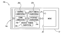
- FIG. 1 shows a lab-on-chip system 10 a according to one illustrated embodiment where one or more subsystems are integrally formed on a substrate 12 .
- the substrate may comprise one or more layers of various materials for example: insulators or dielectrics such as glass, ceramic and/or polycrystalline silicon; conductors such as copper, gold, silver, and/or aluminum; and/or semiconductors such as doped silicon, germanium, gallium arsenide and/or gallium arsenide phosphide.
- the lab-on-chip system 10 a includes a variety of subsystems to handle various aspects of operation.
- the lab-on-chip system 10 a may include one or more antennas 14 a and communications subsystems 16 a coupled to the antenna 14 a to provide wireless communications from and/or to the lab-on-chip system 10 a.
- the antenna 144 a may be formed as one or more conductive traces formed on the substrate 12 .
- the conductive traces may be formed, for example, by depositing and/or etching using standard printed circuit board and/or micro-fabrication techniques (e.g., techniques employed in fabrication of integrated circuits or micro-electrical-mechanical structure (MEMS)). While illustrated as a dipole antenna 14 a, the antenna may take a variety of forms, for example a coil antenna or Yagi antenna, depending on the particular environment and application in which the lab-on-chip will be used.
- MEMS micro-electrical-mechanical structure
- the communications subsystem 16 a may likewise be integrally formed on the substrate 12 using standard printed circuit board and/or micro-fabrication techniques.
- the communications subsystem is formed as a communications circuit such as those commonly associated with passive radio frequency identification (RFID) tags or passive store security tags.
- the communications subsystem may comprises a transmitter 16 c and/or receiver 16 d .
- the transmitter 16 c and receiver 16 d may be formed individually, or may be formed as a transceiver 16 .
- the chip-on-lab system 10 a may also include a passive power subsystem 18 a which may be integrally formed on the substrate 12 using standard printed circuit board and/or micro-fabrication techniques.
- the passive power subsystem 18 a is so denominated because it derives electrical power from electromagnetic fields, for example RF signals, wirelessly received at the antenna 14 a and provides the electrical power to operate one or more of the other subsystems.
- the passive power subsystem 18 a may include a voltage rectifier and/or energy storage device such as a capacitor or ultra capacitor.
- the passive power subsystem 18 a may employ various circuitry and/or techniques from the field of radio-frequency identification (RFID) such as those taught in U.S. Pat. No. 6,429,775; U.S. Pat. No. 5,808,587; and/or U.S. Pat. No. 5,973,598 for deriving power from the wireless signals.
- RFID radio-frequency identification
- the lab-on-chip system 10 a may further include a control subsystem 20 a which may be integrally formed on the substrate 12 using standard printed circuit board and/or micro-fabrication techniques.
- the control subsystem 20 a controls operation of one or more of the other subsystems.
- the control subsystem 20 a may be hardwired, in a form similar to an application specific integrated circuit (ASIC).
- ASIC application specific integrated circuit
- the control subsystem 20 a may execute instructions provided in a program or other software routine, in a form similar to a microcontroller or microprocessor.
- the instructions may be stored in a memory such as a register, read-only memory (ROM) and/or a random access memory (RAM) which may be formed as part of the control subsystem 20 a, or may be distinct therefrom.
- the memory of the control subsystem 20 a may be preconfigured or programmed with instructions and/or may receive instructions via the antenna 14 a and communications subsystem 16 a.
- the lab-on-chip system 10 a may further include a self check subsystem 22 a which may be integrally formed in the substrate 12 using common printed circuit board and/or micro-fabrication techniques.
- the self check subsystem 22 a executes self check tests of one or more subsystems, and may even perform a self check test on the self check subsystem 22 a itself.
- the self check subsystem 22 a may provide results of one or more self check tests from the lab-on-chip system 10 a via the communications subsystem 16 a and antenna 14 a .
- the self check subsystem may be hardwired in a fashion similar to an ASIC, or may execute instructions stored in a memory such as a register, ROM or RAM which may form a portion of the self check subsystem 22 a or may be distinct therefrom.
- the lab-on-chip system 10 a may further include an interface subsystem 24 a to interface which may be integrally formed in the substrate 12 using common printed circuit board and/or micro-fabrication techniques.
- the interface subsystem 24 a interfaces with one or more MEMS devices 26 , for example, pumps, valves, electrodes, channels, sensors 27 and/or other transducers. Some specific examples of MEMS devices are discussed below with reference to FIGS. 5-9 .
- FIGS. 3 and 4 show a lab-on-chip system 10 b according to another illustrated embodiment in which one or more subsystems are discretely formed as one or more separate wafers or chips 30 , which are placed, soldered or otherwise located on the substrate 12 .
- the wafer(s) or chip(s) 30 may be packaged or unpackaged, and may be mounted to the substrate 12 using any of a variety of mounting techniques, for example, via flip chip techniques.
- the wafer or chip 30 may be physically and/or logically partitioned into separate subsystems such as a communications subsystem 16 b, control subsystem 20 b, self check subsystem 22 b and interface subsystem 24 b.
- the lab-on-chip system 10 b may include a communications port 28 to physically and communicatingly couple an off-substrate antenna 14 b to the communications subsystem 16 b carried by the substrate 12 .
- the lab-on-chip system 10 b may employ a discrete power source 18 b such as one or more battery cells and/or ultra capacitors.
- the discrete power source 18 b may take the place of the passive power subsystem 18 a ( FIG. 1 ) or may be provided in addition to the passive power subsystem 18 a.
- the substrate 12 may carry one or more MEMS devices.
- the MEMS devices may, for example, include one or more channels 32 formed in one or more layers of the substrate 12 .
- the channels 32 may be formed to contain and/or direct movement of one or more fluid bodies 34 as is commonly understood in the field of MEMS technology and particularly in the field of microfluidic technology.
- the lab-on-chip system 10 b may include a cover 36 to at least partially enclose the channel 32 and/or protect elements of the various subsystems or buses interconnecting the various subsystems.
- the cover 36 may take the form of glass or another insulative material, and may or may not be transparent.
- the MEMS devices may include one or more sensors 27 operable to sense or detect one or more operating characteristics of one or more MEMS devices and/or one or more physical characteristics of the work product.
- the sensors may take a variety of forms.
- rotational encoders and/or optical sensors may be employed to detect the movement and/or position of work products such as fluid bodies, agents, reagents, and/or samples.
- Rotational encoders and/or optical sensors may additionally or alternatively be employed to detect the movement and/or position of various components of the MEMS devices such as gears, valves and/or actuators.
- inductive sensors similar to those employed in touch screen devices may be employed to detect movement, position, and/or pressure of one of the work products or MEMS devices.
- chemical sensors may be employed to, for example, detect the occurrence or results of a chemical or biological reaction.
- Accelometers may be employed to detect the rate of change or force of a work product or MEMS device.
- Voltage sensors, current sensors, resistivity sensors may be employed to detect various electrical characteristics of one or more work products and/or one or more MEMS devices. As will be readily apparent to those of ordinary skill in the art, the types of sensors should not be limited to those disclosed herein.
- FIG. 5 shows an embodiment of a MEMS device 26 particularly useful in microfluidics operations such as electrowetting.
- the MEMS device 26 comprises a plurality of electrodes 38 spaced about a portion of the substrate 12 and selectively actuable to apply a potential to a portion of the fluid body 34 .
- the substrate 12 may comprise one or more layers, for example a base 12 a and a fluid compatibility coating or layer 12 b.
- the fluid compatibility layer 12 b may comprise a hydrophobic material to achieve the desired interaction between the fluid body 34 , and the substrate 12 , for example, to achieve a desired contact angle between the fluid body 34 and the substrate 12 .
- the hydrophobic material may be a dielectric, and may overlay the electrodes 38 to electrically insulate the same.
- the fluid compatibility layer 12 b may alternatively comprise a hydrophilic material, which may or may not constitute a dielectric.
- the cover 36 may comprise one or more layers, for example glass 36 a and a conductive layer 362 b such as transparent Indium Tin Oxide (“ITO”) which may serve as a ground electrode to provide a ground potential to the fluid body 34 .
- the control subsystem 20 may include a controller 20 c to control the operation of the electrodes 38 and gate drive circuitry 20 d to transform the instructions from the controller 20 c to control signals for driving individual ones of the electrodes 38 . By sequentially activating electrodes 38 , the fluid body 34 can be moved from a first position (shown in solid line) to a second position (shown in broken line).
- FIG. 6 shows another MEMS device 26 particularly useful in microfluidics operations such as electrophoreses. Many of the elements of FIG. 6 are similar or analogous to the elements of FIG. 5 so will not be discussed in detail.
- the fluid body 34 includes one or more particles 46 suspended in the fluid body 34 , such as in a colloidal suspension. Activation of the electrodes 38 may cause the particles 46 to migrate through the fluid body 34 , as is commonly known in electrophoreses.
- FIG. 7 shows a further embodiment of the MEMS device 26 in the form of a silicon check valve pump.
- a lower portions 12 a of the substrate 12 may support a patterned layer 12 c to form an inlet valve 50 a and an outlet valve 50 b which cooperates with a silicon member 52 to form the silicon check valve pump.
- FIG. 8 shows still a further embodiment of a MEMS device 26 in the form of fixed geometry valve pump.
- the substrate 12 is patterned to form a number of channels defining inlet diffuser elements 56 a and outlet diffuser elements 56 b.
- a pair of piezoelectric drive disks 58 are operable to pump fluid from the inlet diffuser elements to the outlet diffuser elements 56 b.
- FIG. 9 shows yet a further MEMS device 26 in the form of a micro-gear pump.
- the substrate 12 is patterned to form an inlet 60 a and an outlet 60 b with a channel extending therebetween.
- the pair of intermeshing gears 62 a, 62 b are electromagnetically operable to move fluid from the inlet 60 a to the outlet 60 b.
- FIG. 10 shows a manufacturing environment 70 suitable for manufacturing lab-on-chip systems 10 a , 10 b (collectively 10 ) according to one illustrated embodiment.
- the manufacturing environment 70 may include one or more clean rooms 72 housing manufacturing equipment such as equipment typically associated with the micro-fabrication industry.
- One or more depositioning devices 72 a may be employed for depositing various layers on the substrate 12 .
- One or more masking devices 72 b may be employed for masking various layers of the substrate 12 .
- One or more etching devices 72 c may be employed for etching the various layers of the substrate 12 .
- One or more cutting devices (not shown) may be employed for cutting the substrate 12 or a wafer in which the substrate resides.
- One or more pick and place devices 72 d may be employed to automatically pick packaged or unpackaged chips and place the chips on the substrate 12 .
- a manufacturing control system 74 may control operation of one or more of the manufacturing devices 72 a - 72 d.
- the manufacturing control system 74 may include one or more antennas, transmitters, receivers, or transceivers, commonly referred to as interrogators, positioned throughout the clean room 72 .
- a first antenna 74 a and/or transceiver 74 b may be positioned proximate or otherwise associated with the depositioning device 72 a.
- a second antenna 74 c and/or transceiver 74 d may be positioned proximate or otherwise associated with the masking device 72 b.
- a third antenna 74 e and/or transceiver 74 f may be positioned proximate or otherwise associated with the etching device 72 c.
- a fourth antenna 74 g and/or transceiver 74 h may be positioned proximate or otherwise associated with the pick and place machinery 72 d.
- the manufacturing control system 74 may also include one or more manufacturing computing systems 74 i.
- the transceivers 74 b, 74 d , 74 f , 74 h may provide signals or information received from the lab-on-chip systems 10 to the computing system 74 i.
- the transceivers 74 b, 74 d, 74 f, 74 h may additionally, or alternatively provide signals or information received from the manufacturing computing system 74 i to the lab-on-chip systems 10 .
- the manufacturing computing system 74 i may be programmed to control manufacturing operation based on the information received from the individual lab-on-chip systems 10 , for example, the results of self check tests performed on the various lab-on-chip systems 10 .
- FIG. 10 illustrates a one-to-one pairing between the manufacturing devices 72 a - 72 d and antenna and transceiver combinations
- FIG. 10 illustrates a one-to-one pairing between the manufacturing devices 72 a - 72 d and antenna and transceiver combinations
- FIG. 10 illustrates a one-to-one pairing between the manufacturing devices 72 a - 72 d and antenna and transceiver combinations
- the particular typology will depend on the particular layout of the manufacturing environment 70 as well as the signal strength of antennas and transceivers of both the manufacturing control system 74 and the lab-on-chip systems 10 .
- FIG. 11 shows a laboratory or other environment 76 suitable for using the lab-on-chip systems 10 .
- the laboratory environment 76 may include a laboratory system 78 to analyze information resulting from operation of the lab-on-chip system 10 .
- the laboratory system 78 may include one or more antennas 78 a positioned to communicate with the lab-on-chip system 10 , one or more transmitters, receivers, or transceivers commonly known as interrogators 78 b communicatingly coupled to the antenna 78 a, and one or more laboratory computing systems 78 c coupled to receive and process information received from the lab-on-chip system 10 via the antenna 78 and transceiver 78 b.
- the laboratory computing system 78 c may include one or more programs for analyzing data collected by the lab-on-chip system 10 .
- the laboratory environment 76 may also include one or more automated laboratory devices 80 operable to physically interact with the lab-on-chip system 10 .
- the laboratory device 80 may provide agents, reagents, samples or other materials to the lab-on-chip system 10 , for example, via a pipette array dispenser.
- the laboratory device 80 may be under control of the laboratory computing system 78 c, or may be operated independently thereof.
- the laboratory device 80 may further include sensors such as optical devices to sense various physical characteristics of the lab-on-chip system 10 .
- FIGS. 12A-12C show a method 100 a of manufacturing a lab-on-chip system 10 a according to one illustrated embodiment, starting at 102 .
- the method 100 a is discussed with reference to various elements of the lab-on-chip systems 10 a illustrated in FIG. 1 and the manufacturing environment 70 illustrated in FIG. 10 .
- the substrate 12 is provided in the manufacturing environment 72 ( FIG. 10 ).
- the various manufacturing devices 72 a - 72 c form the self check subsystem 22 a on the substrate 12 .
- the various manufacturing devices 72 a - 72 c form the communications subsystem 16 a on the substrate 12 .
- the various manufacturing devices 72 a - 72 c form the antenna 14 a on the substrate 12 .
- the self check subsystem 22 a performs a self check test of itself.
- the self check subsystem 22 a performs a self check test of the communications subsystem 16 a.
- the communications subsystem 16 a transmits results of the self check test via the antenna 14 a.
- the manufacturing computing system 74 i determines if there is a faulty subsystem. If a faulty subsystem exists, at 120 the manufacturing computing system 74 i identifies the faulty lab-on-chip system 10 a, and at 122 discontinues manufacture of the faulty lab-on-chip system 10 a. If a faulty subsystem does not exist, control passes to 124 a.
- the manufacturing devices 72 a - 72 c form the control subsystem 20 a on the substrate 12 .
- the self check subsystem 22 a performs a self check of the control subsystem 20 a.
- the communications subsystem 16 a transmit the results of the self check test via the antenna 14 a.
- the manufacturing computing system 74 i determines if a faulty subsystem exists. If a faulty subsystem exists, the manufacturing computing system 74 i identifies the faulty lab-on-chip system 10 a at 120 and discontinues manufacture of the faulty lab-on-chip system 10 a at 122 . If a faulty subsystem does not exist, control passes to 132 a.
- the manufacturing devices 72 a - 72 c form a MEMS interface subsystem 24 a on the substrate 12 .
- the self check subsystem 22 a performs a self check test of the MEMS interface subsystem 24 a.
- the communications subsystem 16 a transmits the results of the self check test via the antenna 14 a.
- the manufacturing computing system 74 i determines if a faulty subsystem exists. If a faulty subsystem exists, the manufacturing computing system 74 i identifies the faulty lab-on-chip system 10 a at 120 and discontinues manufacture the faulty lab-on-chip system 10 a at 122 . If a faulty subsystem does not exist, control passes to 140 a.
- the manufacturing devices 72 a - 72 c form the passive power subsystem 18 a on the substrate. 12 .
- the self check subsystem 22 a performs a self check test on the passive power system 18 .
- the communications subsystem 16 a transmits results of the self check test via antenna 14 a, 14 b.
- the manufacturing computing system 74 i determines if a faulty subsystem exists if a faulty subsystem exists, the manufacturing computing system 74 i identifies the faulty lab-on-chip system 10 a at 120 and discontinues manufacture of the faulty lab-on-chip system 10 a at 122 . If a faulty subsystem does not exist, control passes to 148 .
- the manufacturing devices 72 a - 72 c form MEMS devices 26 on the substrate, for example one or more pumps, valves, gears, and/or electrodes.
- the self check subsystem 22 a performs a self check test of the MEMS structures 26 .
- the self check test subsystem 22 a performs a self check test of the interoperability of subsystems 16 a, 18 a, 20 a, 22 a, 24 a, 26 .
- the self check test of interoperability of subsystems may be performed following each self check test of the individual subsystems.
- the communications subsystem 16 a transmits results of the self check test via the antenna 14 a.
- the manufacturing computing system 74 i determines if there is a faulty subsystem or lab-on-chip system 10 a. If a subsystem is faulty or the interoperability of the subsystems s faulty the manufacturing computing device 74 a identifies the faulty lab-on-chip system 10 a at 120 and discontinues manufacture of the faulty lab-on-chip system 10 a at 122 . If the subsystems and interoperability of the subsystems are not faulty, manufacturing is completed at 158 .
- FIGS. 13A-13C show a method 100 b of manufacturing a lab-on-chip system 10 b according to one illustrated embodiment, starting at 102 .
- the method 100 b is discussed with reference to various elements of the lab-on-chip systems lob illustrated in FIGS. 3 and 4 , as well as the manufacturing environment 70 illustrated in FIG. 10 .
- Many of the acts in the method 100 b are similar or identical to those of method 100 a, thus common reference numerals are used to identify such.
- the method 100 b assumes that each subsystem is provided independently. In some embodiments, some or all of the subsystems may be provided as a single integrated circuit, which may be packaged or unpackaged.
- the substrate 12 is provided in the manufacturing environment 72 ( FIG. 10 ).
- manufacturing devices such as pick and place machinery 72 d locate the self check subsystem 22 b on the substrate 12 .
- manufacturing devices such as pick and place machinery 72 d locate the communications subsystem 16 b on the substrate 12 .
- a communications port 28 is formed in the substrate 12 , for example, using the various manufacturing devices 72 a - 72 d.
- manufacturing devices such as pick and place machinery 72 d couple the antenna 14 b to the communications port 28 .
- the self check subsystem 22 b performs a self check test of itself.
- the self check subsystem 22 b performs a self check test of the communications subsystem 16 b.
- the communications subsystem 16 b transmits results of the self check test via the antenna 14 b.
- the manufacturing computing system 74 i determines if there is a faulty subsystem. If a faulty subsystem exists, at 120 the manufacturing computing system 74 i identifies the faulty lab-on-chip system 10 b, and at 122 discontinues manufacture of the faulty lab-on-chip system 10 b. If a faulty subsystem does not exist, control passes to 124 b.
- manufacturing devices such as pick and place machinery 72 d locate the control subsystem 20 b on the substrate 12 .
- the self check subsystem 22 b performs a self check of the control subsystem 20 b.
- the communications subsystem 16 b transmit the results of the self check test via the antenna 14 b.
- the manufacturing computing system 74 i determines if a faulty subsystem exists. If a faulty subsystem exists, the manufacturing computing system 74 i identifies the faulty lab-on-chip system 10 b at 120 and discontinues manufacture of the faulty lab-on-chip system 10 b at 122 . If a faulty subsystem does not exist, control passes to 132 b.
- manufacturing devices such as pick and place machinery 72 d locate a MEMS interface subsystem 24 b on the substrate 12 .
- the self check subsystem 22 b performs a self check test of the MEMS interface subsystem 24 b.
- the communications subsystem 16 b transmits the results of the self check test via the antenna 14 b.
- the manufacturing computing system 74 i determines if a faulty subsystem exists. If a faulty subsystem exists, the manufacturing computing system 74 i identifies the faulty lab-on-chip system 10 b at 120 and discontinues manufacture of the faulty lab-on-chip system 10 b at 122 . If a faulty subsystem does not exist, control passes to 140 b.
- manufacturing devices such as pick and place machinery 72 d locate the passive power subsystem 18 b on the substrate 12 .
- the self check subsystem 22 b performs a self check test on the passive power system 18 b .
- the communications subsystem 16 b transmits results of the self check test via antenna 14 b.
- the manufacturing computing system 74 i determines if a faulty subsystem exists. If a faulty subsystem exists, the manufacturing computing system 74 i identifies the faulty lab-on-chip system 10 b at 120 and discontinues manufacture of the faulty lab-on-chip system 10 b at 122 . If a faulty subsystem does not exist, control passes to 148 .
- the manufacturing devices 72 a - 72 c form MEMS devices 26 on the substrate 12 , for example one or more pumps, valves, gears, and/or electrodes.
- the self check subsystem 22 b performs a self check test of the MEMS structures 26 .
- the self check test subsystem 22 b performs a self check test of the interoperability of subsystems 16 b, 18 b, 20 b, 22 b, 24 b , 26 b.
- the self check test of interoperability of subsystems may be performed following each self check test of the individual subsystems.
- the communications subsystem 16 b transmits results of the self check test via the antenna 14 b.
- the manufacturing computing system 74 i determines if there is a faulty subsystem or lab-on-chip system 10 b. If a subsystem is faulty or the interoperability of the subsystems is faulty the manufacturing computing device 74 a identifies the faulty lab-on-chip system 10 b at 120 and discontinues manufacture of the faulty lab-on-chip system 10 b at 122 . If the subsystems and lab-on-chip system 10 b are not faulty, manufacturing is completed at 158 .
- FIG. 14 shows a method 200 of operating a lab-on-chip system 10 according to one illustrated embodiment, starting at 202 .
- the method 200 is discussed with reference to various elements of the lab-on-chip systems 10 illustrated in FIGS. 1 , 3 and the laboratory environment 76 illustrated in FIG. 11 .
- an electromagnetic field is received at the antenna 14 of the lab-on-chip system 10 .
- the electromagnetic field may, for example, take the form of a wireless signal.
- the passive power subsystem 18 a if any, converts the electromagnetic field to electric power.
- the passive power subsystem 18 a supplies electrical power to one or more of the other subsystems 16 a, 20 a , 22 a, 24 a, 26 .
- the discrete power source 18 b may supplied power to one or more of the other subsystems 16 a, 20 a, 22 a, 24 a, 26 .
- the self check subsystem 22 may optionally perform a self check of one or more of the subsystems and/or interoperability of the subsystems.
- the self check subsystem 22 and/or the control subsystem 20 determines if there is a faulty subsystem or if the lab-on-chip system 10 is faulty. If a fault is detected, at 214 the communications subsystem 16 encodes and transmits a fault message via the antenna 14 and the method terminates at 216 .
- control system 20 decodes instructions, if any, contained in the wireless signal.
- the control subsystem 20 controls operation of the various subsystems according to instructions previously provided or received via the wireless signal.
- one or more sensors sense operating characteristics of the MEMS and/or physical characteristics of the work product such as fluid body 34 or particles 46 suspended in the fluid body 34 .
- the communications subsystem 16 a encodes and transmits the sensed characteristics to the laboratory computing system 78 c via the antenna 14 , antenna 78 a, and transceiver 78 b .
- the control subsystem 20 a saves the sensed characteristics to memory.
- certain embodiments may provide distinct advantages over conventional lab-on-chip systems.
- self check testing allows faults to be discovered during manufacturing or during use.
- defects may be detected and manufacturing operations ceased or revised to eliminate useless manufacturing operations, thereby reducing costs and/or increasing manufacturing throughput.
- fatal defects in an earlier manufactured subsystem may be caught before subsequent subsystems are manufactured.
- the lab-on-chip system 10 with the faulty subsystem may be marked or otherwise identified and further manufacturing operations on the particular lab-on-chip system avoided.
- a substitute subsystem for the faulty subsystem may be manufactured or activated (e.g., coupled into with the other subsystems, for example, during the manufacture of those other subsystems).
- wireless transmission may eliminate the need for complicated and costly physical connections.
- the use of a passive power subsystem may extend the useful life of the lab-on-chip system, since such will not depend on the life of a battery.
- the use of wireless transmission may also allow control over the operation of the lab-on-chip system, include reprogramming. Further, the use of wireless communications significantly enhances the ability toe perform self check testing in the manufacturing environment, where physical connections would be difficult, if even possible.
- the teachings provided herein of the invention can be applied to other MEMS devices, not necessarily the exemplary MEMS devices generally described above.
- the lab-on-chip system may include fewer or additional subsystems, and elements from one embodiment may be used with other embodiments. For example, some of the subsystems of a lab-on-chip system 10 may be integrally formed with each other, while other ones of the subsystems are provided as discrete packages.
- control, self check and MEMS interface subsystems 20 , 22 , 24 may be formed as a an integrated circuit on the substrate 12
- the communications subsystem 16 and/or passive power subsystem 18 a may be formed as one or more discrete components and located on the substrate.
- signal bearing media include, but are not limited to, the following: recordable type media such as floppy disks, hard disk drives, CD ROMs, digital tape, and computer memory; and transmission type media such as digital and analog communications links using TDM or IP based communications links (e.g., packet links).
Abstract
Description
Claims (44)
Priority Applications (1)
| Application Number | Priority Date | Filing Date | Title |
|---|---|---|---|
| US10/909,920 US7395474B2 (en) | 2003-08-01 | 2004-08-02 | Lab-on-chip system and method and apparatus for manufacturing and operating same |
Applications Claiming Priority (2)
| Application Number | Priority Date | Filing Date | Title |
|---|---|---|---|
| US49212503P | 2003-08-01 | 2003-08-01 | |
| US10/909,920 US7395474B2 (en) | 2003-08-01 | 2004-08-02 | Lab-on-chip system and method and apparatus for manufacturing and operating same |
Publications (2)
| Publication Number | Publication Date |
|---|---|
| US20050066246A1 US20050066246A1 (en) | 2005-03-24 |
| US7395474B2 true US7395474B2 (en) | 2008-07-01 |
Family
ID=34316337
Family Applications (1)
| Application Number | Title | Priority Date | Filing Date |
|---|---|---|---|
| US10/909,920 Active 2025-10-20 US7395474B2 (en) | 2003-08-01 | 2004-08-02 | Lab-on-chip system and method and apparatus for manufacturing and operating same |
Country Status (1)
| Country | Link |
|---|---|
| US (1) | US7395474B2 (en) |
Cited By (5)
| Publication number | Priority date | Publication date | Assignee | Title |
|---|---|---|---|---|
| US20060267167A1 (en) * | 2004-10-25 | 2006-11-30 | Mccain Joseph H | Microelectronic device with integrated energy source |
| US20070029994A1 (en) * | 2005-08-05 | 2007-02-08 | Semiconductor Energy Laboratory Co., Ltd. | Semiconductor device and inspection method of semiconductor device and wireless chip |
| US8237548B2 (en) | 2010-06-01 | 2012-08-07 | The Boeing Company | Structural health management device and associated system and method |
| US20140263613A1 (en) * | 2013-03-15 | 2014-09-18 | Horse Sense Shoes, Llc | Board test system and method |
| CN106497777A (en) * | 2016-09-22 | 2017-03-15 | 苏州百源基因技术有限公司 | A kind of self-checking system of real-time fluorescence quantitative PCR instrument and its self checking method |
Families Citing this family (9)
| Publication number | Priority date | Publication date | Assignee | Title |
|---|---|---|---|---|
| PL1709750T3 (en) * | 2004-01-27 | 2015-03-31 | Altivera L L C | Diagnostic radio frequency identification sensors and applications thereof |
| KR101270180B1 (en) * | 2004-01-30 | 2013-05-31 | 가부시키가이샤 한도오따이 에네루기 켄큐쇼 | An inspection apparatus, inspenction method, and method for manufacturing a semiconductor device |
| US20060174177A1 (en) * | 2005-02-02 | 2006-08-03 | Weinstein Michael J | Apparatus and method for using MEMS filters to test electronic circuits |
| US9134221B2 (en) | 2009-03-10 | 2015-09-15 | The Regents Of The University Of California | Fluidic flow cytometry devices and particle sensing based on signal-encoding |
| EP2411810B1 (en) | 2009-03-23 | 2020-10-14 | Siemens Healthcare Nederland B.V. | Manipulation of magnetic particles in a biological sample |
| WO2012054904A2 (en) * | 2010-10-21 | 2012-04-26 | The Regents Of The University Of California | Microfluidics with wirelessly powered electronic circuits |
| WO2014062719A2 (en) | 2012-10-15 | 2014-04-24 | Nanocellect Biomedical, Inc. | Systems, apparatus, and methods for sorting particles |
| EP4248203A1 (en) * | 2020-11-17 | 2023-09-27 | Regents of the University of Minnesota | Wirelessly powered electric actuation of particles and molecules |
| CN115407181B (en) * | 2022-11-02 | 2022-12-23 | 季华实验室 | LED chip nondestructive testing device |
Citations (17)
| Publication number | Priority date | Publication date | Assignee | Title |
|---|---|---|---|---|
| US4979506A (en) | 1989-08-08 | 1990-12-25 | Siemens-Pacesetter, Inc. | Self-test system and method for external programming device |
| US5808587A (en) | 1994-03-24 | 1998-09-15 | Hochiki Corporation | Wireless access control system using a proximity member and antenna equipment therefor |
| US5973598A (en) | 1997-09-11 | 1999-10-26 | Precision Dynamics Corporation | Radio frequency identification tag on flexible substrate |
| US6294997B1 (en) | 1999-10-04 | 2001-09-25 | Intermec Ip Corp. | RFID tag having timing and environment modules |
| US6429775B1 (en) | 1996-04-03 | 2002-08-06 | Intermec Ip Corp. | Apparatus for transporting radio frequency power to energize radio frequency identification transponders |
| US6499006B1 (en) * | 1999-07-14 | 2002-12-24 | Wireless Valley Communications, Inc. | System for the three-dimensional display of wireless communication system performance |
| US6667725B1 (en) * | 2002-08-20 | 2003-12-23 | The United States Of America As Represented By The Administrator Of The National Aeronautics And Space Administration | Radio frequency telemetry system for sensors and actuators |
| US6728916B2 (en) | 2001-05-23 | 2004-04-27 | International Business Machines Corporation | Hierarchical built-in self-test for system-on-chip design |
| US6747556B2 (en) | 2001-07-31 | 2004-06-08 | Medtronic Physio-Control Corp. | Method and system for locating a portable medical device |
| US6804552B2 (en) * | 2000-11-03 | 2004-10-12 | Medtronic, Inc. | MEMs switching circuit and method for an implantable medical device |
| US6882128B1 (en) * | 2000-09-27 | 2005-04-19 | Science Applications International Corporation | Method and system for energy reclamation and reuse |
| US6917099B2 (en) * | 2003-08-27 | 2005-07-12 | Hewlett-Packard Development Company, L.P. | Die carrier with fluid chamber |
| US6950193B1 (en) * | 1997-10-28 | 2005-09-27 | Rockwell Automation Technologies, Inc. | System for monitoring substrate conditions |
| US7034660B2 (en) * | 1999-02-26 | 2006-04-25 | Sri International | Sensor devices for structural health monitoring |
| US7090471B2 (en) * | 2003-01-15 | 2006-08-15 | California Institute Of Technology | Integrated electrostatic peristaltic pump method and apparatus |
| US7096068B2 (en) | 2002-01-17 | 2006-08-22 | Cardiac Pacemakers, Inc. | User-attachable or detachable telemetry module for medical devices |
| US7201846B2 (en) * | 2002-02-13 | 2007-04-10 | Hospira, Inc. | Micro-fluidic anti-microbial filter |
-
2004
- 2004-08-02 US US10/909,920 patent/US7395474B2/en active Active
Patent Citations (18)
| Publication number | Priority date | Publication date | Assignee | Title |
|---|---|---|---|---|
| US4979506A (en) | 1989-08-08 | 1990-12-25 | Siemens-Pacesetter, Inc. | Self-test system and method for external programming device |
| US5808587A (en) | 1994-03-24 | 1998-09-15 | Hochiki Corporation | Wireless access control system using a proximity member and antenna equipment therefor |
| US6429775B1 (en) | 1996-04-03 | 2002-08-06 | Intermec Ip Corp. | Apparatus for transporting radio frequency power to energize radio frequency identification transponders |
| US5973598A (en) | 1997-09-11 | 1999-10-26 | Precision Dynamics Corporation | Radio frequency identification tag on flexible substrate |
| US6950193B1 (en) * | 1997-10-28 | 2005-09-27 | Rockwell Automation Technologies, Inc. | System for monitoring substrate conditions |
| US7034660B2 (en) * | 1999-02-26 | 2006-04-25 | Sri International | Sensor devices for structural health monitoring |
| US6499006B1 (en) * | 1999-07-14 | 2002-12-24 | Wireless Valley Communications, Inc. | System for the three-dimensional display of wireless communication system performance |
| US6294997B1 (en) | 1999-10-04 | 2001-09-25 | Intermec Ip Corp. | RFID tag having timing and environment modules |
| US6882128B1 (en) * | 2000-09-27 | 2005-04-19 | Science Applications International Corporation | Method and system for energy reclamation and reuse |
| US6804552B2 (en) * | 2000-11-03 | 2004-10-12 | Medtronic, Inc. | MEMs switching circuit and method for an implantable medical device |
| US6728916B2 (en) | 2001-05-23 | 2004-04-27 | International Business Machines Corporation | Hierarchical built-in self-test for system-on-chip design |
| US6747556B2 (en) | 2001-07-31 | 2004-06-08 | Medtronic Physio-Control Corp. | Method and system for locating a portable medical device |
| US6937150B2 (en) | 2001-07-31 | 2005-08-30 | Medtronic Physio-Control Manufacturing Corp. | Method and system for locating a portable medical device |
| US7096068B2 (en) | 2002-01-17 | 2006-08-22 | Cardiac Pacemakers, Inc. | User-attachable or detachable telemetry module for medical devices |
| US7201846B2 (en) * | 2002-02-13 | 2007-04-10 | Hospira, Inc. | Micro-fluidic anti-microbial filter |
| US6667725B1 (en) * | 2002-08-20 | 2003-12-23 | The United States Of America As Represented By The Administrator Of The National Aeronautics And Space Administration | Radio frequency telemetry system for sensors and actuators |
| US7090471B2 (en) * | 2003-01-15 | 2006-08-15 | California Institute Of Technology | Integrated electrostatic peristaltic pump method and apparatus |
| US6917099B2 (en) * | 2003-08-27 | 2005-07-12 | Hewlett-Packard Development Company, L.P. | Die carrier with fluid chamber |
Non-Patent Citations (13)
| Title |
|---|
| "Microfabrication Glossary," retrieved Jul. 19, 2004, from http://www.memsnet.org/glossary/. |
| Charlot et al., "Electrically Induce Stimuli for MEMS Self-Test," VLSI Test Symposium, 19th IEEE Proceedings on VTS 2001, May 2001, pp. 210-215. |
| MEMS and Nanotechnology Clearinghouse, "What is MEMS Technology?," retrieved Jul. 19, 2004, from http://www.memsnet.org/mems/what-is.html. |
| Mohseni, K., "MicroPumps-MicroFluidics ASEN 5519," Department of Aerospace Engineering Sciences, University of Colorado at Boulder, Spring 2004. |
| Mutlu, S., "Microfluidic Biochemical Analysis System with Electro-Osmotic Pump and Thermally Responsive Polymer Valve," Faculty Candidate Seminar Announcement, retrieved Jul. 16, 2004, from http://www.azbio.org/news/FacultySeminar.html. |
| Mutlu, S., et al., "Micromachined Porous Polymer for Bubble Free Electro-Osmotic Pump," in Proceedings of the IEEE MEMS Conference, Las Vegas, Jan. 20-24, 2002, pp. 19-24. |
| Su, Y-C., et al., "A Water-Powered Osmotic Microactuator," Journal of Microelectromechanical Systems 11(6):736-742, Dec. 2002. |
| U.S. Appl. No. 10/909,919, filed Aug. 2, 2004, Maltseff et al. |
| U.S. Appl. No. 60/492,123, filed Aug. 1, 2003, Maltseff et al. |
| U.S. Appl. No. 60/492,125, filed Aug. 1, 2003, Maltseff et al. |
| Utah State Center of Excellence for Biomedical Microfluidics, "Detectors," May 11, 2004, retrieved Jul. 16, 2004, from http://www.mems.utah.edu/Project%20Pages/Detector.htm. |
| Utah State Center of Excellence for Biomedical Microfluidics, "Micro-FFF," May 11, 2004, retrieved Jul. 16, 2004, from http://www.mems.utah.edu/Project%20Pages/FFF.htm. |
| Vennemann, P., "Micropumps-Concepts and Design Examples," TUDelft Laboratory for Aero- and Hydrodynamics, Feb. 26, 2004. |
Cited By (13)
| Publication number | Priority date | Publication date | Assignee | Title |
|---|---|---|---|---|
| US9099410B2 (en) | 2003-10-13 | 2015-08-04 | Joseph H. McCain | Microelectronic device with integrated energy source |
| US9413405B2 (en) | 2003-10-13 | 2016-08-09 | Joseph H. McCain | Microelectronic device with integrated energy source |
| US7557433B2 (en) * | 2004-10-25 | 2009-07-07 | Mccain Joseph H | Microelectronic device with integrated energy source |
| US20060267167A1 (en) * | 2004-10-25 | 2006-11-30 | Mccain Joseph H | Microelectronic device with integrated energy source |
| US7669094B2 (en) * | 2005-08-05 | 2010-02-23 | Semiconductor Energy Laboratory Co., Ltd. | Semiconductor device and inspection method of semiconductor device and wireless chip |
| US7937636B2 (en) | 2005-08-05 | 2011-05-03 | Semiconductor Energy Laboratory Co., Ltd. | Semiconductor device and inspection method of semiconductor device and wireless chip |
| US20100123555A1 (en) * | 2005-08-05 | 2010-05-20 | Semiconductor Energy Laboratory Co., Ltd. | Semiconductor device and inspection method of semiconductor device and wireless chip |
| US20070029994A1 (en) * | 2005-08-05 | 2007-02-08 | Semiconductor Energy Laboratory Co., Ltd. | Semiconductor device and inspection method of semiconductor device and wireless chip |
| US8237548B2 (en) | 2010-06-01 | 2012-08-07 | The Boeing Company | Structural health management device and associated system and method |
| US20140263613A1 (en) * | 2013-03-15 | 2014-09-18 | Horse Sense Shoes, Llc | Board test system and method |
| US9087279B2 (en) * | 2013-03-15 | 2015-07-21 | Horse Sense Shoes, Llc | Board test system and method |
| US9377505B2 (en) | 2013-03-15 | 2016-06-28 | Horse Sense Shoes, Llc | Board test system and method |
| CN106497777A (en) * | 2016-09-22 | 2017-03-15 | 苏州百源基因技术有限公司 | A kind of self-checking system of real-time fluorescence quantitative PCR instrument and its self checking method |
Also Published As
| Publication number | Publication date |
|---|---|
| US20050066246A1 (en) | 2005-03-24 |
Similar Documents
| Publication | Publication Date | Title |
|---|---|---|
| US7395474B2 (en) | Lab-on-chip system and method and apparatus for manufacturing and operating same | |
| US7249302B2 (en) | Integrated test-on-chip system and method and apparatus for manufacturing and operating same | |
| US6495104B1 (en) | Indicator components for microfluidic systems | |
| US9023278B2 (en) | Instrumentation systems and methods | |
| US20030180965A1 (en) | Micro-fluidic device and method of manufacturing and using the same | |
| WO2004062801A1 (en) | Multi-layered electrochemical microfluidic sensor comprising reagent on porous layer | |
| WO2007025041A2 (en) | Microfluidic liquid stream configuration system | |
| US8835247B2 (en) | Sensor array and a method of manufacturing the same | |
| US11865543B2 (en) | Multilayer electrical connection for digital microfluidics on substrates | |
| CN103412023A (en) | Electrochemical integrated sensing chip based on digital micro-fluid technology | |
| US20150352548A1 (en) | Addressable actuator system | |
| CN105964314B (en) | A kind of centrifugal type microfludic chip electrochemical detection device | |
| US20100314699A1 (en) | Electrochemical sensor device, method of manufacturing the same | |
| US20230330666A1 (en) | Diagnostic detection chip devices and methods of manufacture and assembly | |
| US7740805B2 (en) | Integrated CMOS-compatible biochip | |
| EP2063987A2 (en) | Assembly of at least one microfluidic device and a mounting piece, mounting piece and methods for manufacture and use of such an assembly | |
| Grenier et al. | Microfluidic on-chip for biomedical applications | |
| US20220234046A1 (en) | Magnetic particle extraction in an ewod instrument | |
| US9527078B2 (en) | Fluid handling device, fluid handling method, and fluid handling system | |
| US11845079B2 (en) | Integrated silicon platform for electronic biosensors | |
| US20230302445A1 (en) | Microfluidic chip and electrical interface for microchip electrophoresis | |
| EP3582894A1 (en) | Microfluidic chip | |
| Hoffmann et al. | Electrochemical Microanalytical System for Ionometric Measurements | |
| EP3976255A1 (en) | Devices and methods for fluid actuation | |
| CN114910538A (en) | Biosensor system and method for analyzing test sample using the same |
Legal Events
| Date | Code | Title | Description |
|---|---|---|---|
| AS | Assignment |
Owner name: INTERMEC IP CORP., CALIFORNIA Free format text: ASSIGNMENT OF ASSIGNORS INTEREST;ASSIGNORS:MALTSEFF, PAUL A.;PAYNE, RONALD D.;REEL/FRAME:015399/0613 Effective date: 20041021 |
|
| FEPP | Fee payment procedure |
Free format text: PAYOR NUMBER ASSIGNED (ORIGINAL EVENT CODE: ASPN); ENTITY STATUS OF PATENT OWNER: LARGE ENTITY |
|
| STCF | Information on status: patent grant |
Free format text: PATENTED CASE |
|
| FPAY | Fee payment |
Year of fee payment: 4 |
|
| FEPP | Fee payment procedure |
Free format text: PAYOR NUMBER ASSIGNED (ORIGINAL EVENT CODE: ASPN); ENTITY STATUS OF PATENT OWNER: LARGE ENTITY Free format text: PAYER NUMBER DE-ASSIGNED (ORIGINAL EVENT CODE: RMPN); ENTITY STATUS OF PATENT OWNER: LARGE ENTITY |
|
| AS | Assignment |
Owner name: LUSATIA FOUNDATION AG L.L.C., DELAWARE Free format text: ASSIGNMENT OF ASSIGNORS INTEREST;ASSIGNOR:INTERMEC IP CORP.;REEL/FRAME:028913/0991 Effective date: 20120725 |
|
| FPAY | Fee payment |
Year of fee payment: 8 |
|
| AS | Assignment |
Owner name: NYTELL SOFTWARE LLC, DELAWARE Free format text: MERGER;ASSIGNOR:LUSATIA FOUNDATION AG L.L.C.;REEL/FRAME:037481/0444 Effective date: 20150826 |
|
| MAFP | Maintenance fee payment |
Free format text: PAYMENT OF MAINTENANCE FEE, 12TH YEAR, LARGE ENTITY (ORIGINAL EVENT CODE: M1553); ENTITY STATUS OF PATENT OWNER: LARGE ENTITY Year of fee payment: 12 |