US7405967B2 - Microelectronic programmable device and methods of forming and programming the same - Google Patents
Microelectronic programmable device and methods of forming and programming the same Download PDFInfo
- Publication number
- US7405967B2 US7405967B2 US11/276,097 US27609706A US7405967B2 US 7405967 B2 US7405967 B2 US 7405967B2 US 27609706 A US27609706 A US 27609706A US 7405967 B2 US7405967 B2 US 7405967B2
- Authority
- US
- United States
- Prior art keywords
- electrode
- ion conductor
- electrodes
- programmable
- accordance
- Prior art date
- Legal status (The legal status is an assumption and is not a legal conclusion. Google has not performed a legal analysis and makes no representation as to the accuracy of the status listed.)
- Expired - Lifetime, expires
Links
Images


Classifications
-
- H—ELECTRICITY
- H04—ELECTRIC COMMUNICATION TECHNIQUE
- H04N—PICTORIAL COMMUNICATION, e.g. TELEVISION
- H04N1/00—Scanning, transmission or reproduction of documents or the like, e.g. facsimile transmission; Details thereof
- H04N1/40—Picture signal circuits
- H04N1/405—Halftoning, i.e. converting the picture signal of a continuous-tone original into a corresponding signal showing only two levels
- H04N1/4051—Halftoning, i.e. converting the picture signal of a continuous-tone original into a corresponding signal showing only two levels producing a dispersed dots halftone pattern, the dots having substantially the same size
-
- G—PHYSICS
- G06—COMPUTING; CALCULATING OR COUNTING
- G06K—GRAPHICAL DATA READING; PRESENTATION OF DATA; RECORD CARRIERS; HANDLING RECORD CARRIERS
- G06K15/00—Arrangements for producing a permanent visual presentation of the output data, e.g. computer output printers
- G06K15/02—Arrangements for producing a permanent visual presentation of the output data, e.g. computer output printers using printers
- G06K15/10—Arrangements for producing a permanent visual presentation of the output data, e.g. computer output printers using printers by matrix printers
- G06K15/102—Arrangements for producing a permanent visual presentation of the output data, e.g. computer output printers using printers by matrix printers using ink jet print heads
- G06K15/105—Multipass or interlaced printing
- G06K15/107—Mask selection
-
- G—PHYSICS
- G11—INFORMATION STORAGE
- G11C—STATIC STORES
- G11C11/00—Digital stores characterised by the use of particular electric or magnetic storage elements; Storage elements therefor
-
- G—PHYSICS
- G11—INFORMATION STORAGE
- G11C—STATIC STORES
- G11C11/00—Digital stores characterised by the use of particular electric or magnetic storage elements; Storage elements therefor
- G11C11/56—Digital stores characterised by the use of particular electric or magnetic storage elements; Storage elements therefor using storage elements with more than two stable states represented by steps, e.g. of voltage, current, phase, frequency
- G11C11/5614—Digital stores characterised by the use of particular electric or magnetic storage elements; Storage elements therefor using storage elements with more than two stable states represented by steps, e.g. of voltage, current, phase, frequency using conductive bridging RAM [CBRAM] or programming metallization cells [PMC]
-
- G—PHYSICS
- G11—INFORMATION STORAGE
- G11C—STATIC STORES
- G11C13/00—Digital stores characterised by the use of storage elements not covered by groups G11C11/00, G11C23/00, or G11C25/00
- G11C13/0002—Digital stores characterised by the use of storage elements not covered by groups G11C11/00, G11C23/00, or G11C25/00 using resistive RAM [RRAM] elements
- G11C13/0009—RRAM elements whose operation depends upon chemical change
- G11C13/0011—RRAM elements whose operation depends upon chemical change comprising conductive bridging RAM [CBRAM] or programming metallization cells [PMCs]
-
- H—ELECTRICITY
- H01—ELECTRIC ELEMENTS
- H01L—SEMICONDUCTOR DEVICES NOT COVERED BY CLASS H10
- H01L27/00—Devices consisting of a plurality of semiconductor or other solid-state components formed in or on a common substrate
- H01L27/02—Devices consisting of a plurality of semiconductor or other solid-state components formed in or on a common substrate including semiconductor components specially adapted for rectifying, oscillating, amplifying or switching and having at least one potential-jump barrier or surface barrier; including integrated passive circuit elements with at least one potential-jump barrier or surface barrier
- H01L27/04—Devices consisting of a plurality of semiconductor or other solid-state components formed in or on a common substrate including semiconductor components specially adapted for rectifying, oscillating, amplifying or switching and having at least one potential-jump barrier or surface barrier; including integrated passive circuit elements with at least one potential-jump barrier or surface barrier the substrate being a semiconductor body
- H01L27/10—Devices consisting of a plurality of semiconductor or other solid-state components formed in or on a common substrate including semiconductor components specially adapted for rectifying, oscillating, amplifying or switching and having at least one potential-jump barrier or surface barrier; including integrated passive circuit elements with at least one potential-jump barrier or surface barrier the substrate being a semiconductor body including a plurality of individual components in a repetitive configuration
- H01L27/101—Devices consisting of a plurality of semiconductor or other solid-state components formed in or on a common substrate including semiconductor components specially adapted for rectifying, oscillating, amplifying or switching and having at least one potential-jump barrier or surface barrier; including integrated passive circuit elements with at least one potential-jump barrier or surface barrier the substrate being a semiconductor body including a plurality of individual components in a repetitive configuration including resistors or capacitors only
-
- H—ELECTRICITY
- H04—ELECTRIC COMMUNICATION TECHNIQUE
- H04N—PICTORIAL COMMUNICATION, e.g. TELEVISION
- H04N1/00—Scanning, transmission or reproduction of documents or the like, e.g. facsimile transmission; Details thereof
- H04N1/46—Colour picture communication systems
- H04N1/52—Circuits or arrangements for halftone screening
-
- H—ELECTRICITY
- H10—SEMICONDUCTOR DEVICES; ELECTRIC SOLID-STATE DEVICES NOT OTHERWISE PROVIDED FOR
- H10B—ELECTRONIC MEMORY DEVICES
- H10B63/00—Resistance change memory devices, e.g. resistive RAM [ReRAM] devices
- H10B63/80—Arrangements comprising multiple bistable or multi-stable switching components of the same type on a plane parallel to the substrate, e.g. cross-point arrays
- H10B63/84—Arrangements comprising multiple bistable or multi-stable switching components of the same type on a plane parallel to the substrate, e.g. cross-point arrays arranged in a direction perpendicular to the substrate, e.g. 3D cell arrays
-
- H—ELECTRICITY
- H10—SEMICONDUCTOR DEVICES; ELECTRIC SOLID-STATE DEVICES NOT OTHERWISE PROVIDED FOR
- H10N—ELECTRIC SOLID-STATE DEVICES NOT OTHERWISE PROVIDED FOR
- H10N70/00—Solid-state devices without a potential-jump barrier or surface barrier, and specially adapted for rectifying, amplifying, oscillating or switching
- H10N70/011—Manufacture or treatment of multistable switching devices
- H10N70/021—Formation of the switching material, e.g. layer deposition
- H10N70/023—Formation of the switching material, e.g. layer deposition by chemical vapor deposition, e.g. MOCVD, ALD
-
- H—ELECTRICITY
- H10—SEMICONDUCTOR DEVICES; ELECTRIC SOLID-STATE DEVICES NOT OTHERWISE PROVIDED FOR
- H10N—ELECTRIC SOLID-STATE DEVICES NOT OTHERWISE PROVIDED FOR
- H10N70/00—Solid-state devices without a potential-jump barrier or surface barrier, and specially adapted for rectifying, amplifying, oscillating or switching
- H10N70/011—Manufacture or treatment of multistable switching devices
- H10N70/021—Formation of the switching material, e.g. layer deposition
- H10N70/026—Formation of the switching material, e.g. layer deposition by physical vapor deposition, e.g. sputtering
-
- H—ELECTRICITY
- H10—SEMICONDUCTOR DEVICES; ELECTRIC SOLID-STATE DEVICES NOT OTHERWISE PROVIDED FOR
- H10N—ELECTRIC SOLID-STATE DEVICES NOT OTHERWISE PROVIDED FOR
- H10N70/00—Solid-state devices without a potential-jump barrier or surface barrier, and specially adapted for rectifying, amplifying, oscillating or switching
- H10N70/011—Manufacture or treatment of multistable switching devices
- H10N70/041—Modification of the switching material, e.g. post-treatment, doping
- H10N70/046—Modification of the switching material, e.g. post-treatment, doping by diffusion, e.g. photo-dissolution
-
- H—ELECTRICITY
- H10—SEMICONDUCTOR DEVICES; ELECTRIC SOLID-STATE DEVICES NOT OTHERWISE PROVIDED FOR
- H10N—ELECTRIC SOLID-STATE DEVICES NOT OTHERWISE PROVIDED FOR
- H10N70/00—Solid-state devices without a potential-jump barrier or surface barrier, and specially adapted for rectifying, amplifying, oscillating or switching
- H10N70/011—Manufacture or treatment of multistable switching devices
- H10N70/061—Patterning of the switching material
- H10N70/063—Patterning of the switching material by etching of pre-deposited switching material layers, e.g. lithography
-
- H—ELECTRICITY
- H10—SEMICONDUCTOR DEVICES; ELECTRIC SOLID-STATE DEVICES NOT OTHERWISE PROVIDED FOR
- H10N—ELECTRIC SOLID-STATE DEVICES NOT OTHERWISE PROVIDED FOR
- H10N70/00—Solid-state devices without a potential-jump barrier or surface barrier, and specially adapted for rectifying, amplifying, oscillating or switching
- H10N70/011—Manufacture or treatment of multistable switching devices
- H10N70/061—Patterning of the switching material
- H10N70/066—Patterning of the switching material by filling of openings, e.g. damascene method
-
- H—ELECTRICITY
- H10—SEMICONDUCTOR DEVICES; ELECTRIC SOLID-STATE DEVICES NOT OTHERWISE PROVIDED FOR
- H10N—ELECTRIC SOLID-STATE DEVICES NOT OTHERWISE PROVIDED FOR
- H10N70/00—Solid-state devices without a potential-jump barrier or surface barrier, and specially adapted for rectifying, amplifying, oscillating or switching
- H10N70/011—Manufacture or treatment of multistable switching devices
- H10N70/061—Patterning of the switching material
- H10N70/068—Patterning of the switching material by processes specially adapted for achieving sub-lithographic dimensions, e.g. using spacers
-
- H—ELECTRICITY
- H10—SEMICONDUCTOR DEVICES; ELECTRIC SOLID-STATE DEVICES NOT OTHERWISE PROVIDED FOR
- H10N—ELECTRIC SOLID-STATE DEVICES NOT OTHERWISE PROVIDED FOR
- H10N70/00—Solid-state devices without a potential-jump barrier or surface barrier, and specially adapted for rectifying, amplifying, oscillating or switching
- H10N70/20—Multistable switching devices, e.g. memristors
- H10N70/24—Multistable switching devices, e.g. memristors based on migration or redistribution of ionic species, e.g. anions, vacancies
- H10N70/245—Multistable switching devices, e.g. memristors based on migration or redistribution of ionic species, e.g. anions, vacancies the species being metal cations, e.g. programmable metallization cells
-
- H—ELECTRICITY
- H10—SEMICONDUCTOR DEVICES; ELECTRIC SOLID-STATE DEVICES NOT OTHERWISE PROVIDED FOR
- H10N—ELECTRIC SOLID-STATE DEVICES NOT OTHERWISE PROVIDED FOR
- H10N70/00—Solid-state devices without a potential-jump barrier or surface barrier, and specially adapted for rectifying, amplifying, oscillating or switching
- H10N70/801—Constructional details of multistable switching devices
- H10N70/821—Device geometry
- H10N70/823—Device geometry adapted for essentially horizontal current flow, e.g. bridge type devices
-
- H—ELECTRICITY
- H10—SEMICONDUCTOR DEVICES; ELECTRIC SOLID-STATE DEVICES NOT OTHERWISE PROVIDED FOR
- H10N—ELECTRIC SOLID-STATE DEVICES NOT OTHERWISE PROVIDED FOR
- H10N70/00—Solid-state devices without a potential-jump barrier or surface barrier, and specially adapted for rectifying, amplifying, oscillating or switching
- H10N70/801—Constructional details of multistable switching devices
- H10N70/821—Device geometry
- H10N70/826—Device geometry adapted for essentially vertical current flow, e.g. sandwich or pillar type devices
- H10N70/8265—Device geometry adapted for essentially vertical current flow, e.g. sandwich or pillar type devices on sidewalls of dielectric structures, e.g. mesa or cup type devices
-
- H—ELECTRICITY
- H10—SEMICONDUCTOR DEVICES; ELECTRIC SOLID-STATE DEVICES NOT OTHERWISE PROVIDED FOR
- H10N—ELECTRIC SOLID-STATE DEVICES NOT OTHERWISE PROVIDED FOR
- H10N70/00—Solid-state devices without a potential-jump barrier or surface barrier, and specially adapted for rectifying, amplifying, oscillating or switching
- H10N70/801—Constructional details of multistable switching devices
- H10N70/841—Electrodes
- H10N70/8416—Electrodes adapted for supplying ionic species
-
- H—ELECTRICITY
- H10—SEMICONDUCTOR DEVICES; ELECTRIC SOLID-STATE DEVICES NOT OTHERWISE PROVIDED FOR
- H10N—ELECTRIC SOLID-STATE DEVICES NOT OTHERWISE PROVIDED FOR
- H10N70/00—Solid-state devices without a potential-jump barrier or surface barrier, and specially adapted for rectifying, amplifying, oscillating or switching
- H10N70/801—Constructional details of multistable switching devices
- H10N70/881—Switching materials
- H10N70/882—Compounds of sulfur, selenium or tellurium, e.g. chalcogenides
- H10N70/8822—Sulfides, e.g. CuS
-
- H—ELECTRICITY
- H10—SEMICONDUCTOR DEVICES; ELECTRIC SOLID-STATE DEVICES NOT OTHERWISE PROVIDED FOR
- H10N—ELECTRIC SOLID-STATE DEVICES NOT OTHERWISE PROVIDED FOR
- H10N70/00—Solid-state devices without a potential-jump barrier or surface barrier, and specially adapted for rectifying, amplifying, oscillating or switching
- H10N70/801—Constructional details of multistable switching devices
- H10N70/881—Switching materials
- H10N70/882—Compounds of sulfur, selenium or tellurium, e.g. chalcogenides
- H10N70/8825—Selenides, e.g. GeSe
-
- G—PHYSICS
- G06—COMPUTING; CALCULATING OR COUNTING
- G06K—GRAPHICAL DATA READING; PRESENTATION OF DATA; RECORD CARRIERS; HANDLING RECORD CARRIERS
- G06K2215/00—Arrangements for producing a permanent visual presentation of the output data
- G06K2215/0082—Architecture adapted for a particular function
- G06K2215/0094—Colour printing
-
- G—PHYSICS
- G11—INFORMATION STORAGE
- G11C—STATIC STORES
- G11C13/00—Digital stores characterised by the use of storage elements not covered by groups G11C11/00, G11C23/00, or G11C25/00
- G11C13/04—Digital stores characterised by the use of storage elements not covered by groups G11C11/00, G11C23/00, or G11C25/00 using optical elements ; using other beam accessed elements, e.g. electron or ion beam
-
- G—PHYSICS
- G11—INFORMATION STORAGE
- G11C—STATIC STORES
- G11C2207/00—Indexing scheme relating to arrangements for writing information into, or reading information out from, a digital store
- G11C2207/10—Aspects relating to interfaces of memory device to external buses
- G11C2207/104—Embedded memory devices, e.g. memories with a processing device on the same die or ASIC memory designs
-
- G—PHYSICS
- G11—INFORMATION STORAGE
- G11C—STATIC STORES
- G11C2213/00—Indexing scheme relating to G11C13/00 for features not covered by this group
- G11C2213/10—Resistive cells; Technology aspects
- G11C2213/15—Current-voltage curve
-
- G—PHYSICS
- G11—INFORMATION STORAGE
- G11C—STATIC STORES
- G11C2213/00—Indexing scheme relating to G11C13/00 for features not covered by this group
- G11C2213/50—Resistive cell structure aspects
- G11C2213/51—Structure including a barrier layer preventing or limiting migration, diffusion of ions or charges or formation of electrolytes near an electrode
-
- G—PHYSICS
- G11—INFORMATION STORAGE
- G11C—STATIC STORES
- G11C2213/00—Indexing scheme relating to G11C13/00 for features not covered by this group
- G11C2213/50—Resistive cell structure aspects
- G11C2213/55—Structure including two electrodes, a memory active layer and at least two other layers which can be a passive or source or reservoir layer or a less doped memory active layer
-
- G—PHYSICS
- G11—INFORMATION STORAGE
- G11C—STATIC STORES
- G11C2213/00—Indexing scheme relating to G11C13/00 for features not covered by this group
- G11C2213/70—Resistive array aspects
- G11C2213/72—Array wherein the access device being a diode
-
- G—PHYSICS
- G11—INFORMATION STORAGE
- G11C—STATIC STORES
- G11C2213/00—Indexing scheme relating to G11C13/00 for features not covered by this group
- G11C2213/70—Resistive array aspects
- G11C2213/79—Array wherein the access device being a transistor
-
- H—ELECTRICITY
- H10—SEMICONDUCTOR DEVICES; ELECTRIC SOLID-STATE DEVICES NOT OTHERWISE PROVIDED FOR
- H10B—ELECTRONIC MEMORY DEVICES
- H10B63/00—Resistance change memory devices, e.g. resistive RAM [ReRAM] devices
- H10B63/20—Resistance change memory devices, e.g. resistive RAM [ReRAM] devices comprising selection components having two electrodes, e.g. diodes
-
- H—ELECTRICITY
- H10—SEMICONDUCTOR DEVICES; ELECTRIC SOLID-STATE DEVICES NOT OTHERWISE PROVIDED FOR
- H10B—ELECTRONIC MEMORY DEVICES
- H10B63/00—Resistance change memory devices, e.g. resistive RAM [ReRAM] devices
- H10B63/30—Resistance change memory devices, e.g. resistive RAM [ReRAM] devices comprising selection components having three or more electrodes, e.g. transistors
-
- Y—GENERAL TAGGING OF NEW TECHNOLOGICAL DEVELOPMENTS; GENERAL TAGGING OF CROSS-SECTIONAL TECHNOLOGIES SPANNING OVER SEVERAL SECTIONS OF THE IPC; TECHNICAL SUBJECTS COVERED BY FORMER USPC CROSS-REFERENCE ART COLLECTIONS [XRACs] AND DIGESTS
- Y10—TECHNICAL SUBJECTS COVERED BY FORMER USPC
- Y10S—TECHNICAL SUBJECTS COVERED BY FORMER USPC CROSS-REFERENCE ART COLLECTIONS [XRACs] AND DIGESTS
- Y10S438/00—Semiconductor device manufacturing: process
- Y10S438/933—Germanium or silicon or Ge-Si on III-V
Definitions
- 60/231,343 entitled COMMON ELECTRODE CONFIGURATIONS OF THE PROGRAMMABLE METALLIZATION CELL, filed Sep. 8, 2000
- U.S. patent application Ser. No. 60/231,350 entitled ULTRA LOW ENERGY PROGRAMMABLE METALLIZATION CELL DEVICES AND METHODS OF FORMING THE SAME, filed Sep. 8, 2000
- 60/231,427 entitled ELECTRODES FOR THE PROGRAMMABLE METALLIZATION CELL, filed Sep. 8, 2000
- 60/282,045 entitled OPTIMIZED ELECTRODES FOR THE PROGRAMMABLE METALLIZATION CELL, filed Apr. 6, 2001
- U.S. patent application Ser. No. 60/283,591 entitled OPTIMIZED GLASS COMPOSITION FOR THE PROGRAMMABLE METALLIZATION CELL, filed Apr. 13, 2001
- the present invention generally relates to microelectronic devices. More particularly, the invention relates to programmable microelectronic structures suitable for use in integrated circuits.
- Memory devices are often used in electronic systems and computers to store information in the form of binary data. These memory devices may be characterized into various types, each type having associated with it various advantages and disadvantages.
- RAM random access memory
- DRAM Dynamic RAM
- SRAM Static RAM
- PROM programmable read-only memory
- WORM write-once read-many
- PROM devices include erasable PROM (“EPROM”) and electrically erasable PROM (EEPROM) devices, which are alterable after an initial programming.
- EPROM devices generally require an erase step involving exposure to ultra violet light prior to programming the device. Thus, such devices are generally not well suited for use in portable electronic devices.
- EEPROM devices are generally easier to program, but suffer from other deficiencies. In particular, EEPROM devices are relatively complex, are relatively difficult to manufacture, and are relatively large. Furthermore, a circuit including EEPROM devices must withstand the high voltages necessary to program the device. Consequently, EEPROM cost per bit of memory capacity is extremely high compared with other means of data storage.
- Another disadvantage of EEPROM devices is that, although they can retain data without having the power source connected, they require relatively large amounts of power to program. This power drain can be considerable in a compact portable system powered by a battery.
- the present invention provides improved microelectronic devices for use in integrated circuits. More particularly, the invention provides relatively non-volatile, programmable devices suitable for memory and other integrated circuits.
- the present invention provides a programmable device that is relatively easy and inexpensive to manufacture, and which is relatively easy to program.
- a programmable structure includes an ion conductor and at least two electrodes.
- the structure is configured such that when a bias is applied across two electrodes, one or more electrical properties of the structure change.
- a resistance across the structure changes when a bias is applied across the electrodes.
- a capacitance or other electrical property of the structure changes upon application of a bias across the electrodes. One or more of these electrical changes may suitably be detected.
- stored information may be retrieved from a circuit including the structure.
- a programmable structure includes an ion conductor, at least two electrodes, and a barrier interposed between at least a portion of one of the electrodes and the ion conductor.
- the barrier material includes a material configured to reduce diffusion of ions between the ion conductor and at least one electrode. The diffusion barrier may also serve to prevent undesired electrodeposit growth within a portion of the structure.
- the barrier material includes an insulating material. Inclusion of an insulating material increases the voltage required to reduce the resistance of the device.
- the barrier includes material that conducts ions, but which is relatively resistant to the conduction of electrons. Use of such material may reduce undesired plating at an electrode and increase the thermal stability of the device.
- a programmable microelectronic structure is formed on a surface of a substrate by forming a first electrode on the substrate, depositing a layer of ion conductor material over the first electrode, and depositing conductive material onto the ion conductor material.
- a solid solution including the ion conductor and excess conductive material is formed by dissolving (e.g., via thermal and/or photodissolution) a portion of the conductive material in the ion conductor.
- only a portion of the conductive material is dissolved, such that a portion of the conductive material remains on a surface of the ion conductor to form an electrode on a surface of the ion conductor material.
- a programmable structure is formed within a through-hole or via in an insulating material.
- a first electrode feature is formed on a surface of a substrate, insulating material is deposited onto a surface of the electrode feature, a via is formed within the insulating material, and a portion of the programmable structure is formed within the via.
- a portion of the structure within the via is formed by depositing an ion conductive material onto the conductive material, depositing a second electrode material onto the ion conductive material, and, if desired, removing any excess electrode, ion conductor, and/or insulating material.
- only the ion conductor is formed within the via.
- a first electrode is formed below the insulating material an in contact with the ion conductor and the second electrode is formed above the insulating material and in contact with the ion conductor.
- the configuration of the via may be changed to alter (e.g., reduce) a contact area between one or more of the electrodes and the ion conductor. Reducing the cross-sectional area of the interface between the ion conductor and the electrode increases the efficiency of the device (change in electrical property per amount of power supplied to the device).
- the via may extend through the lower electrode to reduce the interface area between the electrode and the ion conductor.
- a portion of the ion conductor may be removed from the via or the ion conductor material may be directionally deposited into only a portion of the via to further reduce an interface between an electrode and the ion conductor.
- a programmable device may be formed on a surface of a substrate.
- a programmable structure includes a floating electrode interposed between two additional electrodes.
- multiple programmable devices are coupled together using a common electrode (e.g., a common anode or a common cathode).
- a common electrode e.g., a common anode or a common cathode.
- multiple programmable devices share a common electrode.
- a capacitance of a programmable structure is altered by causing ions within an ion conductor of the structure to migrate.
- FIG. 1 is a cross-sectional illustration of a programmable structure formed on a surface of a substrate in accordance with the present invention
- FIG. 2 is a cross-sectional illustration of a programmable structure in accordance with an alternative embodiment of the present invention
- FIG. 3 is a current-voltage diagram illustrating current and voltage characteristics of the device illustrated in FIG. 2 in an “on” and “off” state;
- FIG. 4 is a cross-sectional illustration of a programmable structure in accordance with yet another embodiment of the present invention.
- FIG. 5 is a schematic illustration of a portion of a memory device in accordance with an exemplary embodiment of the present invention.
- FIG. 6 is a schematic illustration of a portion of a memory device in accordance with an alternative embodiment of the present invention.
- FIGS. 7 and 8 are a cross-sectional illustrations of a programmable structure having an ion conductor/electrode contact interface formed about a perimeter of the ion conductor in accordance with another embodiment of the present invention
- FIGS. 9 and 10 are a cross-sectional illustrations of a programmable structure having an ion conductor/electrode contact interface formed about a perimeter of the ion conductor in accordance with yet another embodiment of the present invention.
- FIGS. 11 and 12 illustrate a programmable device having a horizontal configuration in accordance with the present invention
- FIGS. 13-19 illustrate programmable device structures with reduced electrode/ion conductor interface surface area in accordance with the present invention
- FIG. 20 illustrates a programmable device with a tapered ion conductor in accordance with the present invention
- FIGS. 21-24 illustrate a programmable device including a floating electrode in accordance with the present invention.
- FIGS. 25-29 illustrate common electrode programmable device structures in accordance with the present invention.
- the present invention generally relates to microelectronic devices. More particularly, the invention relates to programmable structures or devices suitable for various integrated circuit applications.
- FIGS. 1 and 2 illustrate programmable microelectronic structures 100 and 200 formed on a surface of a substrate 110 in accordance with an exemplary embodiment of the present invention.
- Structures 100 and 200 include electrodes 120 and 130 , an ion conductor 140 , and optionally include buffer or barrier layers 155 and/or 255 .
- structures 100 and 200 are configured such that when a bias greater than a threshold voltage (V T ), discussed in more detail below, is applied across electrodes 120 and 130 , the electrical properties of structure 100 change.
- V T threshold voltage
- conductive ions within ion conductor 140 begin to migrate and form an electrodeposit (e.g., electrodeposit 160 ) at or near the more negative of electrodes 120 and 130 ; such an electrodeposit, however, is not required to practice the present invention.
- electrodeposit as used herein means any area within the ion conductor that has an increased concentration of reduced metal or other conductive material compared to the concentration of such material in the bulk ion conductor material. As the electrodeposit forms, the resistance between electrodes 120 and 130 decreases, and other electrical properties may also change. In the absence of any insulating barriers, which are discussed in more detail below, the threshold voltage required to grow the electrodeposit from one electrode toward the other and thereby significantly reduce the resistance of the device is approximately the redox potential of the system, typically a few hundred millivolts. If the same voltage is applied in reverse, the electrodeposit will dissolve back into the ion conductor and the device will return to a high resistance state.
- application of an electric field between electrodes 120 and 130 may cause ions dissolved within conductor 140 to migrate and thus cause a change in the electrical properties of device 100 , without the formation of an electrodeposit.
- Structures 100 and 200 may be used to store information and thus may be used in memory circuits.
- structure 100 or other programmable structures in accordance with the present invention may suitably be used in memory devices to replace DRAM, SRAM, PROM, EPROM, or EEPROM devices.
- programmable structures of the present invention may be used for other applications where programming or changing of electrical properties of a portion of an electrical circuit are desired.
- Substrate 110 may include any suitable material.
- substrate 110 may include semiconductive, conductive, semiinsulative, insulative material, or any combination of such materials.
- substrate 110 includes an insulating material 112 and a portion 114 including microelectronic devices formed on a semiconductor substrate. Layers 112 and 114 may be separated by additional layers (not shown) such as, for example, layers typically used to form integrated circuits. Because the programmable structures can be formed over insulating or other materials, the programmable structures of the present invention are particularly well suited for applications where substrate (e.g., semiconductor material) space is a premium.
- Electrodes 120 and 130 may be formed of any suitable conductive material.
- electrodes 120 and 130 may be formed of doped polysilicon material or metal.
- one of electrodes 120 and 130 is formed of a material including a metal that dissolves in ion conductor 140 when a sufficient bias (V ⁇ V T ) is applied across the electrodes (oxidizable electrode) and the other electrode is relatively inert and does not dissolve during operation of the programmable device (an indifferent electrode).
- electrode 120 may be an anode during a write process and be comprised of a material including silver that dissolves in ion conductor 140 and electrode 130 may be a cathode during the write process and be comprised of an inert material such as tungsten, nickel, molybdenum, platinum, metal silicides, and the like.
- Having at least one electrode formed of a material including a metal which dissolves in ion conductor 140 facilitates maintaining a desired dissolved metal concentration within ion conductor 140 , which in turn facilitates rapid and stable electrodeposit 160 formation within ion conductor 140 or other electrical property change during use of structure 100 and/or 200 .
- use of an inert material for the other electrode facilitates electrodissolution of any electrodeposit that may have formed and/or return of the programmable device to an erased state after application of a sufficient voltage.
- dissolution of any electrodeposit that may have formed preferably begins at or near the oxidizable electrode/electrodeposit interface.
- Initial dissolution of the electrodeposit at the oxidizable electrode/electrodeposit interface may be facilitated by forming structure 100 such that the resistance of the at the oxidizable electrode/electrodeposit interface is greater than the resistance at any other point along the electrodeposit, particularly, the interface between the electrodeposit and the indifferent electrode.
- One way to achieve relatively low resistance at the indifferent electrode is to form the electrode of relatively inert, non-oxidizing material such as platinum. Use of such material reduces formation of oxides at the interface between ion conductor 140 and the indifferent electrode as well as the formation of compounds or mixtures of the electrode material and ion conductor 140 material, which typically have a higher resistance than ion conductor 140 or the electrode material.
- Relatively low resistance at the indifferent electrode may also be obtained by forming a barrier layer between the oxidizable electrode (anode during a write operation), wherein the barrier layer is formed of material having a relatively high resistance.
- Exemplary high resistance materials include layers (e.g., layer 155 and/or layer 255 ) of ion conducting material (e.g., Ag x O, Ag x S, Ag x Se, Ag x Te, where x ⁇ 2, Ag y I, where x ⁇ 1, CuI 2 , CuO, CuS, CuSe, CuTe, GeO 2 , or SiO 2 ) interposed between ion conductor 140 and a metal layer such as silver.
- ion conducting material e.g., Ag x O, Ag x S, Ag x Se, Ag x Te, where x ⁇ 2, Ag y I, where x ⁇ 1, CuI 2 , CuO, CuS, CuSe, CuTe, GeO 2 , or SiO 2
- Reliable growth and dissolution of an electrodeposit can also be facilitated by providing a roughened indifferent electrode surface (e.g., a root mean square roughness of greater than about 1 nm) at the electrode/ion conductor interface.
- the roughened surface may be formed by manipulating film deposition parameters and/or by etching a portion of one of the electrode of ion conductor surfaces.
- relatively high electrical fields form about the spikes or peaks of the roughened surface, and thus the electrodeposits are more likely to form about the spikes or peaks.
- more reliable and uniform changes in electrical properties for an applied voltage across electrodes 120 and 130 may be obtained by providing a roughed interface between the indifferent electrode (cathode during a write operation) and ion conductor 140 .
- Oxidizable electrode material may have a tendency to thermally dissolve or diffuse into ion conductor 140 , particularly during fabrication and/or operation of structure 100 .
- the thermal diffusion is undesired because it may reduce the resistance of structure 100 and thus reduce the change of an electrical property during use of structure 100 .
- the oxidizable electrode includes a metal intercalated in a transition metal sulfide or selenide material such as A x (MB 2 ) 1-x , where A is Ag or Cu, B is S or Se, M is a transition metal such as Ta, V, and Ti, and x ranges from about 0.1 to about 0.7.
- the intercalated material mitigates undesired thermal diffusion of the metal (Ag or Cu) into the ion conductor material, while allowing the metal to participate in the electrodeposit growth upon application of a sufficient voltage across electrodes 120 and 130 .
- the TaS 2 film when silver in intercalated into a TaS 2 film, can include up to about 66.8 atomic percent silver.
- the A x (MB 2 ) 1-x material is preferably amorphous to prevent to prevent undesired diffusion of the metal though the material.
- the amorphous material may be formed by, for example, physical vapor deposition of a target material comprising A x (MB 2 ) 1-x .
- ⁇ -AgI is another suitable material for the oxidizable electrode, as well as the indifferent electrode. Similar to the A x (MB 2 ) 1-x material discussed above, ⁇ -AgI can serve as a source of Ag during operation of structure 100 —e.g., upon application of a sufficient bias, but the silver in the AgI material does not readily thermally diffuse into ion conductor 140 . AgI has a relatively low activation energy for conduction of electricity and does not require doping to achieve relatively high conductivity. When the oxidizable electrode is formed of AgI, depletion of silver in the AgI layer may arise during operation of structure 100 , unless excess silver is provided to the electrode.
- One way to provide the excess silver is to form a silver layer adjacent the AgI layer as discussed above when AgI is used as a buffer layer.
- the AgI layer e.g., layer 155 and/or 255 ) reduces thermal diffusion of Ag into ion conductor 140 , but does not significantly affect conduction of Ag during operation of structure 100 .
- use of AgI increases the operational efficiency of structure 100 because the AgI mitigates non-Faradaic conduction (conduction of electrons that do not participate in the electrochemical reaction).
- buffer layers 155 and/or 255 include GeO 2 and SiO x .
- Amorphous GeO 2 is relatively porous an will “soak up” silver during operation of device 100 , but will retard the thermal diffusion of silver to ion conductor 140 , compared to structures or devices that do not include a buffer layer.
- GeO 2 may be formed by exposing ion conductor 140 to an oxidizing environment at a temperature of about 300° C. to about 800° C. or by exposing ion conductor 140 to an oxidizing environment in the presence of radiation having an energy greater than the band gap of the ion conductor material.
- the GeO 2 may also be deposited using physical vapor deposition (from a GeO 2 target) or chemical vapor deposition (from GeH 4 and an O 2 ).
- Buffer layers can also be used to increase a “write voltage” by placing the buffer layer (e.g., GeO 2 or SiO x ) between ion conductor 140 and the indifferent electrode.
- the buffer material allows metal such as silver to diffuse though the buffer and take part in the electrochemical reaction.
- At least one electrode 120 and 130 is formed of material suitable for use as an interconnect metal.
- electrode 130 may form part of an interconnect structure within a semiconductor integrated circuit.
- electrode 130 is formed of a material that is substantially insoluble in material comprising ion conductor 140 .
- Exemplary materials suitable for both interconnect and electrode 130 material include metals and compounds such as tungsten, nickel, molybdenum, platinum, metal silicides, and the like.
- Layers 155 and/or 255 may also include a material that restricts migration of ions between conductor 140 and the electrodes.
- a barrier layer includes conducting material such as titanium nitride, titanium tungsten, a combination thereof, or the like.
- the barrier may be electrically indifferent, i.e., it allows conduction of electrons through structure 100 or 200 , but it does not itself contribute ions to conduction through structure 200 .
- An electrically indifferent barrier may reduce undesired dendrite growth during operation of the programmable device, and thus may facilitate an “erase” or dissolution of electrodeposit 160 when a bias is applied which is opposite to that used to grow the electrodeposit.
- use of a conducting barrier allows for the “indifferent” electrode to be formed of oxidizable material because the barrier prevents diffusion of the electrode material to the ion conductor.
- Ion conductor 140 is formed of material that conducts ions upon application of a sufficient voltage. Suitable materials for ion conductor 140 include glasses and semiconductor materials. In one exemplary embodiment of the invention, ion conductor 140 is formed of chalcogenide material.
- Ion conductor 140 may also suitably include dissolved conductive material.
- ion conductor 140 may comprise a solid solution that includes dissolved metals and/or metal ions.
- conductor 140 includes metal and/or metal ions dissolved in chalcogenide glass.
- An exemplary chalcogenide glass with dissolved metal in accordance with the present invention includes a solid solution of As x S 1-x —Ag, Ge x Se 1-x —Ag, Ge x S 1-x —Ag, As x S 1-x —Cu, Ge x Se 1-x —Cu, Ge x S 1-x —Cu, where x ranges from about 0.1 to about 0.5 other chalcogenide materials including silver, copper, zinc, combinations of these materials, and the like.
- conductor 140 may include network modifiers that affects mobility of ions through conductor 140 .
- materials such as metals (e.g., silver), halogens, halides, or hydrogen may be added to conductor 140 to enhance ion mobility and thus increase erase/write speeds of the structure.
- a solid solution suitable for use as ion conductor 140 may be formed in a variety of ways.
- the solid solution may be formed by depositing a layer of conductive material such as metal over an ion conductive material such as chalcogenide glass and exposing the metal and glass to thermal and/or photo dissolution processing.
- a solid solution of As 2 S 3 —Ag is formed by depositing As 2 S 3 onto a substrate, depositing a thin film of Ag onto the As 2 S 3 , and exposing the films to light having energy greater than the optical gap of the As 2 S 3 ,—e.g., light having a wavelength of less than about 500 nanometers.
- network modifiers may be added to conductor 140 during deposition of conductor 140 (e.g., the modifier is in the deposited material or present during conductor 140 material deposition) or after conductor 140 material is deposited (e.g., by exposing conductor 140 to an atmosphere including the network modifier).
- a solid solution may be formed by depositing one of the constituents onto a substrate or another material layer and reacting the first constituent with a second constituent.
- germanium preferably amorphous
- the germanium may be deposited onto a portion of a substrate and the germanium may be reacted with H 2 Se to form a Ge—Se glass.
- H 2 Se gas or arsenic or germanium can be deposited and reacted with H 2 S gas.
- Silver or other metal can then be added to the glass as described above.
- a solid solution ion conductor 140 is formed by depositing sufficient metal onto an ion conductor material such that a portion of the metal can be dissolved within the ion conductor material and a portion of the metal remains on a surface of the ion conductor to form an electrode (e.g., electrode 120 ).
- an electrode e.g., electrode 120
- solid solutions containing dissolved metals may be directly deposited onto substrate 110 and the electrode then formed overlying the ion conductor.
- the solid solution is formed by photodissolution to form a macrohomogeneous ternary compound and additional metal is added to the solution using thermal diffusion (e.g., in an inert environment at a temperature of about 85° C. to about 150° C.) to form a solid solution containing, for example, about 30 to about 50, and preferably about 34 atomic percent silver.
- thermal diffusion e.g., in an inert environment at a temperature of about 85° C. to about 150° C.
- Ion conductors having a metal concentration above the photodissolution solubility level facilitates formation of electrodeposits that are thermally stable at operating temperatures (typically about 85° C. to about 150° C.) of devices 100 and 200 .
- the solid solution may be formed by thermally dissolving the metal into the ion conductor at the temperature noted above; however, solid solutions formed exclusively from photodissolution are thought to be less homogeneous than films having similar metal concentrations formed using photodissolution and thermal dissolution.
- Ion conductor 140 may also include a filler material, which fills interstices or voids.
- Suitable filler materials include non-oxidizable and non-silver based materials such as a non-conducting, immiscible silicon oxide and/or silicon nitride, having a cross-sectional dimension of less than about 1 nm, which do not contribute to the growth of an electrodeposit.
- the filler material is present in the ion conductor at a volume percent of up to about 5 percent to reduce a likelihood that an electrodeposit will spontaneously dissolve into the supporting ternary material as the device is exposed to elevated temperature, which leads to more stable device operation without compromising the performance of the device.
- Ion conductor 140 may also include filler material to reduce an effective cross-sectional area of the ion conductor.
- concentration of the filler material which may be the same filler material described above but having a cross-sectional dimension up to about 50 nm, is present in the ion conductor material at a concentration of up to about 50 percent by volume.
- the filler material may also include metal such as silver or copper to fill the voids in the ion conductor material.
- ion conductor 140 includes a germanium-selenide glass with silver diffused in the glass.
- Germanium selenide materials are typically formed from selenium and Ge(Se) 4/2 tetrahedra that may combine in a variety of ways.
- Ge is 4-fold coordinated and Se is 2-fold coordinated, which means that a glass composition near Ge 0.20 Se 0.80 will have a mean coordination number of about 2.4. Glass with this coordination number is considered by constraint counting theory to be optimally constrained and hence very stable with respect to devitrification.
- ion conductor 140 includes a glass having a composition of Ge 0.17 Se 0.83 to Ge 0.25 Se 0.75 .
- composition and structure of ion conductor 140 material often depends on the starting or target material used to form the conductor. Generally, it is desired to form a homogenous material layer for conductor 140 to facilitate reliable and repeatable device performance.
- a target for physical vapor deposition of material suitable for ion conductor 140 is formed by selecting a proper ampoule, preparing the ampoule, maintaining proper temperatures during formation of the glass, slow rocking the composition, and quenching the composition.
- volume and wall thickness are important factors for consideration in selecting an ampoule for forming glass.
- the wall thickness must be thick enough to withstand gas pressures that arise during the glass formation process and are preferably thin enough to facilitate heat exchange during the formation process.
- quartz ampoules with a wall thickness of about 1 mm are used to form Se and Te based chalcogenide glasses, whereas quartz ampoules with a wall thickness of about 1.5 mm are used to form sulfur-based chalcogenide glasses.
- the volume of the ampoule is preferably selected such that the volume of the ampoule is about five times greater than the liquid glass precursor material.
- the ampoule is prepared for glass formation, in accordance with one embodiment of the invention, by cleaning the ampoule with hydrofluoric acid, ethanol and acetone, drying the ampoule for at least 24 hours at about 120° C., evacuating the ampoule and heating the ampoule until the ampoule turns a cherry red color and cooling the ampoule under vacuum, filling ampoule with charge and evacuating the ampoule, heating the ampoule while avoiding melting of the constituents to desorb any remaining oxygen, and sealing the ampoule. This process reduces oxygen contamination, which in turn promotes macrohomogeneous growth of the glass.
- the melting temperature of the glass formation process depends on the glass material. In the case of germanium-based glasses, sufficient time for the chalcogen to react at low temperature with all available germanium is desired to avoid explosion at subsequent elevated temperatures (the vapor pressure of Se at 920° C. is 10 ATM. and 20 ATM. for S at 720° C.). To reduce the risk of explosion, the glass formation process begins by ramping the ampoule temperature to about 300° C. for selenium-based glasses (about 200° C. for sulfur-based glasses) over the period of about an hour and maintaining this temperature for about 12 hours. Next, the temperature is elevated slowly (about 0.5° C./min) up to a temperature about 50° C.
- the ampoule remains at about this temperature for about 12 hours.
- the temperature is then elevated to about 940° C. to ensure melting of all non-reacted germanium for Se-based glasses or about 700° C. for S-based glasses.
- the ampoule should remain at this elevated temperature for about 24 hours.
- the melted glass composition is preferably slow rocked at a rate of about 20/minute at least about six hours to increase the homogeneity of the glass.
- Quenching is preferably performed from a temperature at which the vapors and the liquid are in an equilibrium to produce vitrification of the desired composition.
- the quenching temperature is about 50° C. over the liquidus temperature of the glass material.
- Chalcogenide-rich glasses include a range of concentrations in which under-constrained and over-constrained glasses exist.
- the quenching rate has to be fast enough in order to ensure vitrification, e.g., quenching in ice-water or an even stronger coolant such as a mixture of urea and ice-water.
- quenching can be performed in air at about 25° C.
- At least a portion of structure 100 is formed within a via of an insulating material 150 .
- Forming a portion of structure 100 within a via of an insulating material 150 may be desirable because, among other reasons, such formation allows relatively small structures, e.g., on the order of 10 nanometers, to be formed.
- insulating material 150 facilitates isolating various structures 100 from other electrical components.
- Insulating material 150 suitably includes material that prevents undesired diffusion of electrons and/or ions from structure 100 .
- material 150 includes silicon nitride, silicon oxynitride, polymeric materials such as polyimide or parylene, or any combination thereof.
- a contact 165 may suitably be electrically coupled to one or more electrodes 120 , 130 to facilitate forming electrical contact to the respective electrode.
- Contact 165 may be formed of any conductive material and is preferably formed of a metal such as aluminum, aluminum alloys, tungsten, or copper.
- structure 100 is formed by forming electrode 130 on substrate 110 .
- Electrode 130 may be formed using any suitable method such as, for example, depositing a layer of electrode 130 material, patterning the electrode material, and etching the material to form electrode 130 .
- Insulating layer 150 may be formed by depositing insulating material onto electrode 130 and substrate 110 and forming vias in the insulating material using appropriate patterning and etching processes.
- Ion conductor 140 and electrode 120 may then be formed within insulating layer 150 by depositing ion conductor 140 material and electrode 120 material within the via.
- Such ion conductor and electrode material deposition may be selective—i.e., the material is substantially deposited only within the via, or the deposition processes may be relatively non-selective.
- any excess material remaining on a surface of insulating layer 150 may be removed using, for example, chemical mechanical polishing and/or etching techniques.
- Barrier layers 155 and/or 255 may similarly be formed using any suitable deposition and/or etch processes.
- Information may be stored using programmable structures of the present invention by manipulating one or more electrical properties of the structures. For example, a resistance of a structure may be changed from a “0” or off state to a “1” or on state during a suitable write operation. Similarly, the device may be changed from a “1” state to a “0” state during an erase operation.
- the structure may have multiple programmable states such that multiple bits of information are stored in a single structure.
- FIG. 3 illustrates current-voltage characteristics of a programmable structure (e.g. structure 200 ) in accordance with the present invention.
- via diameter, D is about 4 microns
- conductor 140 is about 35 nanometers thick and formed of Ge 3 Se 7 —Ag (near As 8 Ge 3 Se 7 )
- electrode 130 is indifferent and formed of nickel
- electrode 120 is formed of silver
- barrier 255 is a native nickel oxide.
- current through structure 200 in an off state begins to rise upon application of a bias of over about one volt; however, once a write step has been performed (i.e., an electrodeposit has formed), the resistance through conductor 140 drops significantly (i.e., to about 200 ohms), illustrated by curve 320 in FIG. 3 .
- an electrodeposit begins to form near electrode 130 and grow toward electrode 120 .
- An effective threshold voltage i.e., voltage required to cause growth of the electrodeposit and to break through barrier 255 , thereby coupling electrodes 320 , 330 together is relatively high because of barrier 255 .
- a voltage V ⁇ VT must be applied to structure 200 sufficient to cause electrons to tunnel through barrier 255 (when barrier 255 comprises an insulating layer) to form the electrodeposit and to overcome the barrier (e.g., by tunneling through or leakage) and conduct through conductor 140 and at least a portion of barrier 255 .
- an initial “write” threshold voltage is relatively low because no insulative barrier is formed between, for example, ion conductor 140 and either of the electrodes 120 , 130 .
- a state of the device may be read, without significantly disturbing the state, by, for example, applying a forward or reverse bias of magnitude less than a voltage threshold (about 1.4 V for a structure illustrated in FIG. 3 ) for electrodeposition or by using a current limit which is less than or equal to the minimum programming current (the current which will produce the highest of the on resistance values).
- a current limited (to about 1 milliamp) read operation is shown in FIG. 3 . In this case, the voltage is swept from 0 to about 2 V and the current rises up to the set limit (from 0 to 0.2 V), indicating a low resistance (ohmic/linear current-voltage) “on” state.
- Another way of performing a non-disturb read operation is to apply a pulse, with a relatively short duration, which may have a voltage higher than the electrochemical deposition threshold voltage such that no appreciable Faradaic current flows, i.e., nearly all the current goes to polarizing/charging the device and not into the electrodeposition process.
- a programmable structure (e.g., structure 200 ) may suitably be erased by reversing a bias applied during a write operation, wherein a magnitude of the applied bias is equal to or greater than the threshold voltage for electrodeposition in the reverse direction.
- a sufficient erase voltage (V ⁇ V T ) is applied to structure 200 for a period of time which depends on the strength of the initial connection but is typically less than about 1 millisecond to return structure 200 to its “off” state having a resistance well in excess of a million ohms.
- a threshold voltage for erasing the structure is much lower than a threshold voltage for writing the structure because, unlike the write operation, the erase operation does not require electron tunneling through a barrier or barrier breakdown.
- the concentration of conductive material in the ion conductor can be controlled by applying a bias across the programmable device.
- metal such as silver may be taken out of solution by applying a negative voltage in excess of the reduction potential of the conductive material.
- conductive material may be added to the ion conductor (from one of the electrodes) by applying a bias in excess of the oxidation potential of the material.
- the concentration can be reduced by reverse biasing the device to reduce the concentration of the conductive material.
- metal may be added to the solution from the oxidizable electrode by applying a sufficient forward bias. Additionally, it is possible to remove excess metal build up at the indifferent electrode by applying a reverse bias for an extended time or an extended bias over that required to erase the device under normal operating conditions. Control of the conductive material may be accomplished automatically using a suitable microprocessor.
- This technique may also be used to form one of the electrodes from material within the ion conductor material.
- silver from the ion conductor may be plated out to form the oxidizable electrode. This allows the oxidizable electrode to be formed after the device is fully formed and thus mitigates problems associated with conductive material diffusing from the oxidizable electrode during manufacturing of the device.
- multiple bits of data may be stored within a single programmable structure by controlling an amount of electrodeposit which is formed during a write process.
- An amount of electrodeposit that forms during a write process depends on a number of coulombs or charge supplied to the structure during the write process, and may be controlled by using a current limit power source.
- a resistance of a programmable structure is governed by Equation 1, where R on is the “on” state resistance, V T is the threshold voltage for electrodeposition, and I LIM is the maximum current allowed to flow during the write operation.
- the limitation to the amount of information stored in each cell will depend on how stable each of the resistance states is with time. For example, if a structure is with a programmed resistance range of about 3.5 k ⁇ and a resistance drift over a specified time for each state is about ⁇ 250 ⁇ , about 7 equally sized bands of resistance (7 states) could be formed, allowing 3 bits of data to be stored within a single structure. In the limit, for near zero drift in resistance in a specified time limit, information could be stored as a continuum of states, i.e., in analog form.
- structure 400 includes electrodes 420 and 430 , an ion conductor 440 , a contact 460 , and an amorphous silicon diode 470 , such as a Schottky or p-n junction diode, formed between contact 460 and electrode 420 .
- Rows and columns of programmable structures 400 may be fabricated into a high density configuration to provide extremely large storage densities suitable for memory circuits. In general, the maximum storage density of memory devices is limited by the size and complexity of the column and row decoder circuitry.
- a programmable structure storage stack can be suitably fabricated overlying an integrated circuit with the entire semiconductor chip area dedicated to row/column decode, sense amplifiers, and data management circuitry (not shown) since structure 400 need not use any substrate real estate.
- storage densities of many gigabits per square centimeter can be attained using programmable structures of the present invention.
- the programmable structure is essentially an additive technology that adds capability and functionality to existing semiconductor integrated circuit technology.
- FIG. 5 schematically illustrates a portion of a memory device including structure 400 having an isolating p-n junction 470 at an intersection of a bit line 510 and a word line 520 of a memory circuit.
- FIG. 6 illustrates an alternative isolation scheme employing a transistor 610 interposed between an electrode and a contact of a programmable structure located at an intersection of a bit line 610 and a word line 620 of a memory device.
- FIGS. 7-10 illustrate programmable devices in accordance with another embodiment of the invention.
- the devices illustrated in FIGS. 7-10 have an electrode (e.g., the cathode during a write process) with a smaller cross sectional area in contact with the ion conductor compared to the devices illustrated in FIGS. 1-2 and 4 .
- the smaller electrode interface area is thought to increase the efficiency and endurance of the device because an increased percentage of ions in the solid solution are able to take part in the electrodeposit formation process. Thus any cathode plating from ions that do not participate in the electrodeposit process is reduced.
- FIGS. 7 and 8 illustrate a cross sectional and a top cut-away view of a programmable device 700 including an indifferent electrode 710 , an oxidizable electrode 720 , and an ion conductor 730 former overlying an insulating layer 740 such as silicon oxide, silicon nitride, or the like.
- Structure 700 is formed by depositing an indifferent electrode material layer and an insulating layer 750 overlying insulating layer 740 .
- a via is then formed through layer 750 and electrode material layer 710 , using an anisotropic etch process (e.g., reactive ion etching or ion milling) such that the via extends to and/or through a portion of layer 740 .
- the via is then filled with ion conductor material and is suitably doped to form a solid solution as described herein. Any excess ion conductor material is removed from the surface of layer 750 and electrode 730 is formed, for example using a deposition and etch process.
- the indifferent electrode (cathode during write process) area in contact with ion conductor 730 is the surface area of electrode 710 about the perimeter of conductor 730 , rather than the area underlying the ion conductor, as illustrated in FIGS. 1-2 and 4 .
- FIGS. 9 and 10 illustrate a programmable device 900 having an indifferent electrode 910 , an oxidizable electrode 920 , an ion conductor 930 and insulating layers 940 and 950 in accordance with yet another embodiment of the invention.
- Structure 900 is similar to structure 700 , except that once a via is formed through layer 750 , an isotropic etch process (e.g., chemical or plasma) is employed to form the via through electrode 910 , such that a sloped intersection between an ion conductor 930 and electrode 910 is formed.
- an isotropic etch process e.g., chemical or plasma
- FIGS. 11 and 12 illustrate another programmable device 1100 , with a reduced electrode/ion conductor interface, in accordance with the present invention.
- Structure 1100 includes electrodes 1110 and 1120 and an ion conductor 1130 , formed on a surface of an insulating material 1140 , rather than within a via as discussed above.
- the programmable structure is formed by defining an ion conductor 1130 patter on a surface of insulating material 1140 (e.g., using deposition and etch techniques) and forming electrodes 1110 and 1120 , such that the electrodes each contact a portion of the ion conductor.
- the electrodes are formed overlying and in contact with both a portion of the ion conductor and the insulating material.
- the thickness of the layers may be varied in accordance with specific applications of the device, in a preferred embodiment of the invention, the thickness of the ion conductor and electrode films is about 1 nm to about 100 nm.
- Sub-lithographic lateral dimensions of portions of the device may be obtained by overexposing photoresist used to pattern the portions and/or over etching the film layer.
- FIG. 13 illustrates a device 1300 in accordance with yet another embodiment of the invention.
- Structure 1300 is similar to the devices illustrated in FIGS. 7 and 8 , except that the cross-sectional area of the ion conductor that is in contact with the electrodes is reduced by filling a portion of a via with non-ion conductor material, rather than etching through an electrode layer.
- Structure 1300 includes electrodes 1310 and 1320 and an ion conductor 1330 formed within an insulating layer 1340 .
- ion conductor 1330 is formed by creating a trench within insulating layer 1340 , the trench having a diameter indicated by D 2 .
- the trench is then filled using, for example, interference lithography techniques or conformally lining the via with insulating material and using an anisotropic etch process to remove some of the insulating material, leaving a via with a diameter of D 3 .
- Structure 1300 formed using this technique may have a ion conductor cross sectional area as small as about 10 nm in contact with electrodes 1310 and 1320 .
- FIGS. 14-17 illustrate another embodiment of the invention, where the cross sectional area of the ion conductor/electrode interface is relatively small.
- Structure 1400 illustrated in FIG. 14 , includes electrodes 1410 and 1420 and an ion conductor 1430 .
- Structure 1400 is formed in a manner similar to structure 700 , except that the ion conductor material is deposited conformally, using, for example chemical vapor deposition or physical vapor deposition, into a trench, and the trench is not filled with the ion conductor material.
- Structure 1500 is similar to structure 1400 , except that an ion conductor 1530 is formed by etching a portion of ion conductor 1430 , such that a via 1540 is formed through to electrode 1410 .
- Structure 1600 is similar to structure 1500 and is formed by conformally depositing the ion conductor material as described above and then removing the ion conductor material from a surface of insulating material 1450 prior to depositing electrode 1420 material.
- structure 1700 may be formed by selectively deposing the ion conductor 1730 material into only a portion of the trench formed in insulating material 1450 (e.g., using angled deposition and/or shadowing techniques), removing any excess ion conductor material on the surface of insulator 1450 , and forming an electrode 1720 overlying the insulator and in contact with ion conductor 1730 .
- FIGS. 18 and 19 illustrate yet another embodiment of the invention, where a pillar or wall within a trench is used to reduce a cross-sectional area of the interface between the ion conductor and one or more electrodes.
- Structure 1800 illustrated in FIG. 18 , includes electrodes 1810 and 1820 and an ion conductor 1830 formed within an insulating layer 1840 .
- structure 1800 includes a pillar 1850 of insulating material (e.g., insulating material used to form layer 1840 ), formed within a trench within layer 1840 .
- Structure 1800 may be formed using the shadowed deposition technique discussed above.
- Structure 1900 is similar to structure 1800 , except structure 1900 includes a partial pillar 1950 and an ion conductor 1930 , which fills the remaining portion of the formed trench.
- FIG. 20 illustrates yet another structure 2000 in accordance with the present invention.
- Structure 2000 includes electrodes 2010 and 2020 and an ion conductor 2030 formed within an insulating layer 2040 .
- Structure 2000 is formed using an anisotropic or a combination of an anisotropic and an isotropic etch processes to form a tapered via.
- Ion conductor 2030 is then formed within the trench using techniques previously described.
- FIGS. 21-24 illustrate programmable devices in accordance with yet another embodiment of the invention.
- the structures illustrated in FIGS. 21-24 include a floating electrode, which allows multiple bits of information to be stored within a single programmable device.
- Structure 2100 includes a first electrode 2110 , a second, floating electrode 2120 , a third electrode 2130 , ion conductor portions 2140 and 2150 , which may all be formed on a substrate or wholly or partially formed within a via as described above. Although structure 2100 is illustrated in a vertical configuration, the structure may be formed in a horizontal configuration, similar to structure 1100 .
- the first and third electrodes are formed of an indifferent electrode and the second electrode is formed of an oxidizable electrode material.
- the first and third electrodes may be formed of oxidizable electrode material and the second, floating electrode may be formed of an indifferent electrode material.
- the structure includes two “half cells,” where each half cell functions as a programmable device described above in connection with FIG. 1 .
- Each half cell is preferably configured such that the resistance of one half cell differs from the resistance of the other half cell when both cells are in an erased state.
- bits of data may be stored as follows.
- the overall impedance of structure 2100 is approximately equal to the resistance of portions 2140 and 2150 .
- this high resistance state may be represent by the state 00.
- an electrodeposit 2160 will form through conductor portion 2140 from electrode 2110 toward floating electrode 2120 as illustrated in FIG. 22 .
- an electrodeposit will not form within conductor portion 2150 because portion 2150 is under a reverse bias condition and thus will not support growth of an electrodeposit.
- the growth of the electrodeposit will change the impedance of portion 2140 from Z 1 to Z 1 ′, thus changing the overall impedance of structure 2100 , which may be represent by the state 01.
- the current level used to form electrodeposit 2160 should be selected such that it is sufficiently low, allowing the electrodeposit to be dissolved upon application of a sufficient reverse bias.
- a third state may be formed by reversing the polarity of the applied bias across electrodes 2110 and 2130 , such that most of the voltage drop occurs across the high resistance ion conductor portion 2150 and formation of an electrodeposit 2170 begins, as illustrated in FIG. 23 , without causing electrodeposit 2160 to dissolve.
- the impedance of portion 2150 changes from Z 2 to Z 2 ′, and the overall impedance of structure 2100 is Z 1 ′ plus Z 2 ′, which may be represented by the state 11.
- electrodeposit 2160 and/or 2170 may be dissolved by applying a sufficient bias across one or both of the half cells.
- Electrodeposit 2170 can be erased, for example, by sufficiently negatively biasing electrode 2130 with respect to electrode 2110 , which may be represented by a state 00.
- the four possible states, along with the current limit used to form the state, are represented in table 1 below.
- Structure 2100 can be changed to 11 from state 10 by applying a low current limit bias to grow electrodeposit 2150 in portion 2140 .
- structure 2100 can be changed from state 11 to state 01 by dissolving electrodeposit 2170 by applying a relatively high current limit bias such that upper electrode 2130 is positive with respect to lower electrode 2110 .
- structure 2100 can be returned to state 00 using a short current pulse to thermally dissolve electrodeposit 2160 , using a current which is high enough to cause localized heating of the electrodeposit. This will increase the metal concentration in the half-cell but this excess metal can be removed electrically from the cell by plating it back onto the floating electrode. This sequence is summarized in table 2 below.
- structure 2100 can also be used as a noise-tolerant, low energy anti-fuse element for use in field programmable gate arrays (FPGAs) and field configurable circuits and systems.
- FPGAs field programmable gate arrays
- Most physical anti-fuse technologies require large currents and voltages to make a permanent connection.
- the need for such high energy state-switching stimuli is generally considered to be somewhat beneficial as this reduces the likelihood of the anti-fuse accidentally forming a connection in electrically noisy situations.
- the use of high voltages and large currents on chip represent a significant problem as all components in the programming circuits are typically sized accordingly and the high energy consumption reduces battery life in portable systems.
- FIGS. 25-29 illustrate structures in accordance with another embodiment of the invention in which multiple programmable devices include a common electrode (e.g., the devices share a common anode or cathode.
- a common electrode e.g., the devices share a common anode or cathode.
- FIGS. 25 and 26 illustrate a structure 2500 , having a horizontal configuration and a common electrode.
- Structure 2500 includes an electrical connector 2510 coupled to a common surface electrode 2520 , electrodes 2530 and 2540 , and ion conductor portions 2550 and 2560 overlying an insulating layer 2170 .
- Structure 2500 may be used to form word and bit lines as described above by forming a row of electrodes (e.g., anodes) coupled to conductor 2510 , and columns of oppositely bias electrodes (e.g., cathodes) running perpendicular to electrodes 2520 .
- a conductive plug, formed of any suitably conducting material can be used to electrically couple electrode 2520 to conductor 2510 .
- common electrode structures in accordance with this embodiment may be formed using structures having a vertical configuration as described herein.
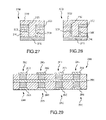
- FIGS. 27 and 28 illustrate additional structures 2700 and 2800 having a common electrode shared between two or more devices
- Structures 2700 and 2800 include a common electrode, electrodes 2720 and 2725 , ion conductors 2730 , 2735 and 2830 , 2835 respectively, and insulating layers 2740 and 2750 .
- Structures 2700 and 2800 may be formed using techniques described above in connection with FIGS. 15 and 16 —e.g., by conformally depositing ion conductor material within a trench of an insulating layer.
- directional deposition may be used to form a structure similar to structure 1700 .
- Structures 2700 and 2800 each include two programmable devices including common electrode 2710 an ion conductor (e.g., conductor 2735 ) and another electrode (e.g., electrode 2725 ).
- Dielectric material 2750 is an insulating material that does not interfere with surface electrodeposit growth, such as silicon oxides, silicon nitrides, and the like.
- FIG. 29 illustrates a structure 2900 including multiple programmable devices 2902 - 2916 formed about a common electrode 2920 .
- Each of the devices 2902 - 2916 may be formed using the method described above in connection with FIG. 21 .
- each of electrodes 2930 - 2936 and 2938 - 2944 may be coupled together in a direction perpendicular to the direction of common electrode 2920 , such that electrode 2920 forms a bit line and electrodes 2930 - 2936 and electrodes 2938 - 2944 form word lines.
- Structure 2900 may operate and be programmed in a manner similar to structure 2100 described above.
- a programmable structure or device stores information by storing a charge as opposed to growing an electrodeposit.
- a capacitance of a structure or device is altered by applying a bias across electrodes of the device such that positively charged ions migrate toward one of the electrodes. If the applied bias is less that a write threshold voltage, no short will form between the electrodes. Capacitance of the structure changes as a result of the ion migration.
- the applied bias is removed, the metal ions tend to diffuse away from the electrode or a barrier proximate the electrode.
- an interface between an ion conductor and a barrier is generally imperfect and includes defects capable of trapping ions. Thus, at least a portion of ions remain at or proximate an interface between a barrier and an ion conductor. If a write voltage is reversed, the ions may suitably be dispersed away from the interface.
- a programmable structure in accordance with the present invention may be used in many applications which would otherwise utilize traditional technologies such as EEPROM, FLASH or DRAM.
- Advantages provided by the present invention over present memory techniques include, among other things, lower production cost and the ability to use flexible fabrication techniques which are easily adaptable to a variety of applications.
- the programmable structures of the present invention are especially advantageous in applications where cost is the primary concern, such as smart cards and electronic inventory tags. Also, an ability to form the memory directly on a plastic card is a major advantage in these applications as this is generally not possible with other forms of semiconductor memories.
- memory elements may be scaled to less than a few square microns in size, the active portion of the device being less than on micron. This provides a significant advantage over traditional semiconductor technologies in which each device and its associated interconnect can take up several tens of square microns.
- the devices of the present invention require relatively low energy and do not require “refreshing.” Thus, the devices are well suitable for portable device applications.
Abstract
Description
| TABLE 1 | ||||||
| Seq | Current | |||||
| # | Polarity | limit | Z half-cell 1 | Z half- |
State/value | |
| 1 | Sub- | | Z1 | Z2 | 00 | |
| |
||||||
| 2 | Upper+ | Low | Z1′ | |
01 | |
| Lower− | ||||||
| 3 | Upper− | Low | Z1′ | Z2′ | 11 | |
| Lower+ | ||||||
| 4 | Upper− | High | Z1 | Z2′ | 10 | |
| Lower+ | ||||||
| TABLE 2 | ||||||
| Seq | Current | |||||
| # | Polarity | limit | Z half-cell 1 | Z half- |
State/value | |
| 4 | Existing | — | Z1 | Z2′ | 10 | |
| state | ||||||
| 5 | Upper+ | Low | Z1′ | Z2′ | 11 | |
| Lower− | ||||||
| 6 | Upper+ | High | Z1′ | |
01 | |
| Lower− | ||||||
| 7 | Upper+ | | Z1 | Z2 | 00 | |
| Lower− | ||||||
Claims (8)
Priority Applications (4)
| Application Number | Priority Date | Filing Date | Title |
|---|---|---|---|
| US11/276,097 US7405967B2 (en) | 1998-12-04 | 2006-02-14 | Microelectronic programmable device and methods of forming and programming the same |
| US12/166,261 US7675766B2 (en) | 2000-02-11 | 2008-07-01 | Microelectric programmable device and methods of forming and programming the same |
| US12/701,060 US7929331B2 (en) | 2000-07-27 | 2010-02-05 | Microelectronic programmable device and methods of forming and programming the same |
| US13/090,193 US8213217B2 (en) | 2000-07-27 | 2011-04-19 | Microelectronic programmable device and methods of forming and programming the same |
Applications Claiming Priority (15)
| Application Number | Priority Date | Filing Date | Title |
|---|---|---|---|
| US55561298A | 1998-12-04 | 1998-12-04 | |
| US09/555,612 US6418049B1 (en) | 1997-12-04 | 1998-12-04 | Programmable sub-surface aggregating metallization structure and method of making same |
| US09/502,915 US6487106B1 (en) | 1999-01-12 | 2000-02-11 | Programmable microelectronic devices and method of forming and programming same |
| US23134600P | 2000-09-08 | 2000-09-08 | |
| US23134500P | 2000-09-08 | 2000-09-08 | |
| US23135000P | 2000-09-08 | 2000-09-08 | |
| US23134300P | 2000-09-08 | 2000-09-08 | |
| US23143200P | 2000-09-08 | 2000-09-08 | |
| US23142700P | 2000-09-08 | 2000-09-08 | |
| US28204501P | 2001-04-06 | 2001-04-06 | |
| US28359101P | 2001-04-13 | 2001-04-13 | |
| US29188601P | 2001-05-18 | 2001-05-18 | |
| US09/951,882 US6635914B2 (en) | 2000-09-08 | 2001-09-10 | Microelectronic programmable device and methods of forming and programming the same |
| US10/452,041 US6998312B2 (en) | 1998-12-04 | 2003-05-30 | Microelectronic programmable device and methods of forming and programming the same |
| US11/276,097 US7405967B2 (en) | 1998-12-04 | 2006-02-14 | Microelectronic programmable device and methods of forming and programming the same |
Related Parent Applications (4)
| Application Number | Title | Priority Date | Filing Date |
|---|---|---|---|
| US09/555,612 Continuation-In-Part US6418049B1 (en) | 1997-12-04 | 1998-12-04 | Programmable sub-surface aggregating metallization structure and method of making same |
| US09/502,915 Continuation-In-Part US6487106B1 (en) | 1998-12-04 | 2000-02-11 | Programmable microelectronic devices and method of forming and programming same |
| US09/951,882 Division US6635914B2 (en) | 1998-12-04 | 2001-09-10 | Microelectronic programmable device and methods of forming and programming the same |
| US10/452,041 Continuation US6998312B2 (en) | 1998-12-04 | 2003-05-30 | Microelectronic programmable device and methods of forming and programming the same |
Related Child Applications (1)
| Application Number | Title | Priority Date | Filing Date |
|---|---|---|---|
| US12/166,261 Continuation US7675766B2 (en) | 2000-02-11 | 2008-07-01 | Microelectric programmable device and methods of forming and programming the same |
Publications (2)
| Publication Number | Publication Date |
|---|---|
| US20060118848A1 US20060118848A1 (en) | 2006-06-08 |
| US7405967B2 true US7405967B2 (en) | 2008-07-29 |
Family
ID=27581172
Family Applications (3)
| Application Number | Title | Priority Date | Filing Date |
|---|---|---|---|
| US09/951,882 Expired - Lifetime US6635914B2 (en) | 1998-12-04 | 2001-09-10 | Microelectronic programmable device and methods of forming and programming the same |
| US10/452,041 Expired - Lifetime US6998312B2 (en) | 1998-12-04 | 2003-05-30 | Microelectronic programmable device and methods of forming and programming the same |
| US11/276,097 Expired - Lifetime US7405967B2 (en) | 1998-12-04 | 2006-02-14 | Microelectronic programmable device and methods of forming and programming the same |
Family Applications Before (2)
| Application Number | Title | Priority Date | Filing Date |
|---|---|---|---|
| US09/951,882 Expired - Lifetime US6635914B2 (en) | 1998-12-04 | 2001-09-10 | Microelectronic programmable device and methods of forming and programming the same |
| US10/452,041 Expired - Lifetime US6998312B2 (en) | 1998-12-04 | 2003-05-30 | Microelectronic programmable device and methods of forming and programming the same |
Country Status (1)
| Country | Link |
|---|---|
| US (3) | US6635914B2 (en) |
Cited By (45)
| Publication number | Priority date | Publication date | Assignee | Title |
|---|---|---|---|---|
| US20080265285A1 (en) * | 2000-02-11 | 2008-10-30 | Axon Technologies Corporation | Microelectronic programmable device and methods of forming and programming the same |
| US20090272960A1 (en) * | 2008-05-02 | 2009-11-05 | Bhaskar Srinivasan | Non-Volatile Resistive Oxide Memory Cells, and Methods Of Forming Non-Volatile Resistive Oxide Memory Cells |
| US20090316467A1 (en) * | 2008-06-18 | 2009-12-24 | Jun Liu | Memory Device Constructions, Memory Cell Forming Methods, and Semiconductor Construction Forming Methods |
| US20100140582A1 (en) * | 2008-12-06 | 2010-06-10 | James Nessel | Chalcogenide nanoionic-based radio frequency switch |
| US20100157688A1 (en) * | 2008-12-23 | 2010-06-24 | Actel Corporation | Push-pull memory cell configured for simultaneous programming of n-channel and p-channel non-volatile transistors |
| US20100208520A1 (en) * | 2009-02-13 | 2010-08-19 | Actel Corporation | Array and control method for flash based fpga cell |
| US20100271863A1 (en) * | 2008-01-15 | 2010-10-28 | Jun Liu | Memory Cells, Memory Cell Programming Methods, Memory Cell Reading Methods, Memory Cell Operating Methods, and Memory Devices |
| US20110002167A1 (en) * | 2009-07-02 | 2011-01-06 | Actel Corporation | Push-pull programmable logic device cell |
| US20110024821A1 (en) * | 2008-12-12 | 2011-02-03 | Actel Corporation | Push-pull fpga cell |
| US20110062408A1 (en) * | 2000-02-11 | 2011-03-17 | Kozicki Michael N | Programmable metallization cell structure including an integrated diode, device including the structure, and method of forming same |
| US8034655B2 (en) | 2008-04-08 | 2011-10-11 | Micron Technology, Inc. | Non-volatile resistive oxide memory cells, non-volatile resistive oxide memory arrays, and methods of forming non-volatile resistive oxide memory cells and memory arrays |
| US20110315947A1 (en) * | 2000-02-11 | 2011-12-29 | Axon Technologies Corporation | Programmable metallization cell structure including an integrated diode, device including the structure, and method of forming same |
| US20120014165A1 (en) * | 2000-02-11 | 2012-01-19 | Axon Technologies Corporation | Optimized solid electrolyte for programmable metallization cell devices and structures |
| US8107273B1 (en) | 2008-07-28 | 2012-01-31 | Adesto Technologies Corporation | Integrated circuits having programmable metallization cells (PMCs) and operating methods therefor |
| US8351242B2 (en) | 2010-09-29 | 2013-01-08 | Micron Technology, Inc. | Electronic devices, memory devices and memory arrays |
| US8411477B2 (en) | 2010-04-22 | 2013-04-02 | Micron Technology, Inc. | Arrays of vertically stacked tiers of non-volatile cross point memory cells, methods of forming arrays of vertically stacked tiers of non-volatile cross point memory cells, and methods of reading a data value stored by an array of vertically stacked tiers of non-volatile cross point memory cells |
| US8427859B2 (en) | 2010-04-22 | 2013-04-23 | Micron Technology, Inc. | Arrays of vertically stacked tiers of non-volatile cross point memory cells, methods of forming arrays of vertically stacked tiers of non-volatile cross point memory cells, and methods of reading a data value stored by an array of vertically stacked tiers of non-volatile cross point memory cells |
| US8431458B2 (en) | 2010-12-27 | 2013-04-30 | Micron Technology, Inc. | Methods of forming a nonvolatile memory cell and methods of forming an array of nonvolatile memory cells |
| US8537592B2 (en) | 2011-04-15 | 2013-09-17 | Micron Technology, Inc. | Arrays of nonvolatile memory cells and methods of forming arrays of nonvolatile memory cells |
| US8624219B1 (en) | 2012-04-12 | 2014-01-07 | Adesto Technologies Corporation | Variable impedance memory element structures, methods of manufacture, and memory devices containing the same |
| US8681531B2 (en) | 2011-02-24 | 2014-03-25 | Micron Technology, Inc. | Memory cells, methods of forming memory cells, and methods of programming memory cells |
| US8742531B2 (en) | 2008-12-08 | 2014-06-03 | Arizona Board Of Regents, Acting For And On Behalf Of Arizona State University | Electrical devices including dendritic metal electrodes |
| US8753949B2 (en) | 2010-11-01 | 2014-06-17 | Micron Technology, Inc. | Nonvolatile memory cells and methods of forming nonvolatile memory cells |
| US8759809B2 (en) | 2010-10-21 | 2014-06-24 | Micron Technology, Inc. | Integrated circuitry comprising nonvolatile memory cells having platelike electrode and ion conductive material layer |
| US8791447B2 (en) | 2011-01-20 | 2014-07-29 | Micron Technology, Inc. | Arrays of nonvolatile memory cells and methods of forming arrays of nonvolatile memory cells |
| US8811063B2 (en) | 2010-11-01 | 2014-08-19 | Micron Technology, Inc. | Memory cells, methods of programming memory cells, and methods of forming memory cells |
| US8999819B2 (en) | 2010-11-14 | 2015-04-07 | Arizona Board of Regents, A Body Corporate of the State of Arizona Acting For on Behalf of Arizona State University | Dendritic metal structures, methods for making dendritic metal structures, and devices including them |
| US9000506B2 (en) | 2010-11-19 | 2015-04-07 | Panasonic Intellectual Property Management Co., Ltd. | Variable resistance nonvolatile memory element and method for manufacturing the same |
| US9147839B2 (en) | 2013-09-05 | 2015-09-29 | Micron Technology, Inc. | Memory cells with recessed electrode contacts |
| US9343665B2 (en) | 2008-07-02 | 2016-05-17 | Micron Technology, Inc. | Methods of forming a non-volatile resistive oxide memory cell and methods of forming a non-volatile resistive oxide memory array |
| US9412421B2 (en) | 2010-06-07 | 2016-08-09 | Micron Technology, Inc. | Memory arrays |
| US9454997B2 (en) | 2010-12-02 | 2016-09-27 | Micron Technology, Inc. | Array of nonvolatile memory cells having at least five memory cells per unit cell, having a plurality of the unit cells which individually comprise three elevational regions of programmable material, and/or having a continuous volume having a combination of a plurality of vertically oriented memory cells and a plurality of horizontally oriented memory cells; array of vertically stacked tiers of nonvolatile memory cells |
| US9773141B2 (en) | 2013-03-12 | 2017-09-26 | Arizona Board Of Regents, A Body Corporate Of The State Of Arizona Acting For And On Behalf Of Arizona State University | Dendritic structures and tags |
| US10128852B2 (en) | 2015-12-17 | 2018-11-13 | Microsemi SoC Corporation | Low leakage ReRAM FPGA configuration cell |
| US10147485B2 (en) | 2016-09-29 | 2018-12-04 | Microsemi Soc Corp. | Circuits and methods for preventing over-programming of ReRAM-based memory cells |
| US10466969B2 (en) | 2017-05-08 | 2019-11-05 | Arizona Board Of Regents On Behalf Of Arizona State University | Tunable true random number generator using programmable metallization cell(s) |
| US10522224B2 (en) | 2017-08-11 | 2019-12-31 | Microsemi Soc Corp. | Circuitry and methods for programming resistive random access memory devices |
| US10546633B2 (en) | 2016-12-09 | 2020-01-28 | Microsemi Soc Corp. | Resistive random access memory cell |
| US10710070B2 (en) | 2015-11-24 | 2020-07-14 | Arizona Board Of Regents On Behalf Of Arizona State University | Low-voltage microfluidic valve device and system for regulating the flow of fluid |
| US10810731B2 (en) | 2014-11-07 | 2020-10-20 | Arizona Board Of Regents On Behalf Of Arizona State University | Information coding in dendritic structures and tags |
| US11127694B2 (en) | 2017-03-23 | 2021-09-21 | Arizona Board Of Regents On Behalf Of Arizona State University | Physical unclonable functions with copper-silicon oxide programmable metallization cells |
| US11244722B2 (en) | 2019-09-20 | 2022-02-08 | Arizona Board Of Regents On Behalf Of Arizona State University | Programmable interposers for electrically connecting integrated circuits |
| US11430233B2 (en) | 2017-06-16 | 2022-08-30 | Arizona Board Of Regents On Behalf Of Arizona State University | Polarized scanning of dendritic identifiers |
| US11598015B2 (en) | 2018-04-26 | 2023-03-07 | Arizona Board Of Regents On Behalf Of Arizona State University | Fabrication of dendritic structures and tags |
| US11935843B2 (en) | 2019-12-09 | 2024-03-19 | Arizona Board Of Regents On Behalf Of Arizona State University | Physical unclonable functions with silicon-rich dielectric devices |
Families Citing this family (175)
| Publication number | Priority date | Publication date | Assignee | Title |
|---|---|---|---|---|
| US6859548B2 (en) | 1996-09-25 | 2005-02-22 | Kabushiki Kaisha Toshiba | Ultrasonic picture processing method and ultrasonic picture processing apparatus |
| US6635914B2 (en) | 2000-09-08 | 2003-10-21 | Axon Technologies Corp. | Microelectronic programmable device and methods of forming and programming the same |
| US6653193B2 (en) | 2000-12-08 | 2003-11-25 | Micron Technology, Inc. | Resistance variable device |
| US6638820B2 (en) | 2001-02-08 | 2003-10-28 | Micron Technology, Inc. | Method of forming chalcogenide comprising devices, method of precluding diffusion of a metal into adjacent chalcogenide material, and chalcogenide comprising devices |
| US6727192B2 (en) | 2001-03-01 | 2004-04-27 | Micron Technology, Inc. | Methods of metal doping a chalcogenide material |
| US6818481B2 (en) | 2001-03-07 | 2004-11-16 | Micron Technology, Inc. | Method to manufacture a buried electrode PCRAM cell |
| US6734455B2 (en) | 2001-03-15 | 2004-05-11 | Micron Technology, Inc. | Agglomeration elimination for metal sputter deposition of chalcogenides |
| US6844608B2 (en) | 2001-05-07 | 2005-01-18 | Advanced Micro Devices, Inc. | Reversible field-programmable electric interconnects |
| US6855977B2 (en) * | 2001-05-07 | 2005-02-15 | Advanced Micro Devices, Inc. | Memory device with a self-assembled polymer film and method of making the same |
| JP4731794B2 (en) | 2001-05-07 | 2011-07-27 | アドバンスト・マイクロ・ディバイシズ・インコーポレイテッド | Switch element having memory effect and method for switching the element |
| US6781868B2 (en) * | 2001-05-07 | 2004-08-24 | Advanced Micro Devices, Inc. | Molecular memory device |
| US6873540B2 (en) * | 2001-05-07 | 2005-03-29 | Advanced Micro Devices, Inc. | Molecular memory cell |
| CN1276518C (en) | 2001-05-07 | 2006-09-20 | 先进微装置公司 | Floating gate memory device using composite molecular material |
| US7102150B2 (en) * | 2001-05-11 | 2006-09-05 | Harshfield Steven T | PCRAM memory cell and method of making same |
| US6838720B2 (en) * | 2001-08-13 | 2005-01-04 | Advanced Micro Devices, Inc. | Memory device with active passive layers |
| US6806526B2 (en) | 2001-08-13 | 2004-10-19 | Advanced Micro Devices, Inc. | Memory device |
| US6858481B2 (en) * | 2001-08-13 | 2005-02-22 | Advanced Micro Devices, Inc. | Memory device with active and passive layers |
| US6737312B2 (en) | 2001-08-27 | 2004-05-18 | Micron Technology, Inc. | Method of fabricating dual PCRAM cells sharing a common electrode |
| US6881623B2 (en) * | 2001-08-29 | 2005-04-19 | Micron Technology, Inc. | Method of forming chalcogenide comprising devices, method of forming a programmable memory cell of memory circuitry, and a chalcogenide comprising device |
| US6955940B2 (en) * | 2001-08-29 | 2005-10-18 | Micron Technology, Inc. | Method of forming chalcogenide comprising devices |
| US6784018B2 (en) | 2001-08-29 | 2004-08-31 | Micron Technology, Inc. | Method of forming chalcogenide comprising devices and method of forming a programmable memory cell of memory circuitry |
| US6646902B2 (en) | 2001-08-30 | 2003-11-11 | Micron Technology, Inc. | Method of retaining memory state in a programmable conductor RAM |
| US6709958B2 (en) | 2001-08-30 | 2004-03-23 | Micron Technology, Inc. | Integrated circuit device and fabrication using metal-doped chalcogenide materials |
| US20030047765A1 (en) * | 2001-08-30 | 2003-03-13 | Campbell Kristy A. | Stoichiometry for chalcogenide glasses useful for memory devices and method of formation |
| US7180104B2 (en) * | 2003-09-03 | 2007-02-20 | Axon Technologies Corporation | Micromechanical structure, device including the structure, and methods of forming and using same |
| US6815818B2 (en) * | 2001-11-19 | 2004-11-09 | Micron Technology, Inc. | Electrode structure for use in an integrated circuit |
| US6791859B2 (en) | 2001-11-20 | 2004-09-14 | Micron Technology, Inc. | Complementary bit PCRAM sense amplifier and method of operation |
| US20030143782A1 (en) | 2002-01-31 | 2003-07-31 | Gilton Terry L. | Methods of forming germanium selenide comprising devices and methods of forming silver selenide comprising structures |
| US6791885B2 (en) | 2002-02-19 | 2004-09-14 | Micron Technology, Inc. | Programmable conductor random access memory and method for sensing same |
| US6847535B2 (en) | 2002-02-20 | 2005-01-25 | Micron Technology, Inc. | Removable programmable conductor memory card and associated read/write device and method of operation |
| US6809362B2 (en) | 2002-02-20 | 2004-10-26 | Micron Technology, Inc. | Multiple data state memory cell |
| US7151273B2 (en) | 2002-02-20 | 2006-12-19 | Micron Technology, Inc. | Silver-selenide/chalcogenide glass stack for resistance variable memory |
| US6849868B2 (en) * | 2002-03-14 | 2005-02-01 | Micron Technology, Inc. | Methods and apparatus for resistance variable material cells |
| US6751114B2 (en) | 2002-03-28 | 2004-06-15 | Micron Technology, Inc. | Method for programming a memory cell |
| US6864500B2 (en) | 2002-04-10 | 2005-03-08 | Micron Technology, Inc. | Programmable conductor memory cell structure |
| US6874335B2 (en) * | 2002-04-12 | 2005-04-05 | Micron Technology, Inc. | Large scale synthesis of germanium selenide glass and germanium selenide glass compounds |
| WO2003094227A1 (en) * | 2002-04-30 | 2003-11-13 | Japan Science And Technology Agency | Solid electrolyte switching device, fpga using same, memory device, and method for manufacturing solid electrolyte switching device |
| US6731528B2 (en) * | 2002-05-03 | 2004-05-04 | Micron Technology, Inc. | Dual write cycle programmable conductor memory system and method of operation |
| US6825135B2 (en) | 2002-06-06 | 2004-11-30 | Micron Technology, Inc. | Elimination of dendrite formation during metal/chalcogenide glass deposition |
| US6890790B2 (en) | 2002-06-06 | 2005-05-10 | Micron Technology, Inc. | Co-sputter deposition of metal-doped chalcogenides |
| US7015494B2 (en) | 2002-07-10 | 2006-03-21 | Micron Technology, Inc. | Assemblies displaying differential negative resistance |
| US6867996B2 (en) * | 2002-08-29 | 2005-03-15 | Micron Technology, Inc. | Single-polarity programmable resistance-variable memory element |
| US7364644B2 (en) * | 2002-08-29 | 2008-04-29 | Micron Technology, Inc. | Silver selenide film stoichiometry and morphology control in sputter deposition |
| US6831019B1 (en) | 2002-08-29 | 2004-12-14 | Micron Technology, Inc. | Plasma etching methods and methods of forming memory devices comprising a chalcogenide comprising layer received operably proximate conductive electrodes |
| US7010644B2 (en) * | 2002-08-29 | 2006-03-07 | Micron Technology, Inc. | Software refreshed memory device and method |
| US6864521B2 (en) | 2002-08-29 | 2005-03-08 | Micron Technology, Inc. | Method to control silver concentration in a resistance variable memory element |
| US7012276B2 (en) * | 2002-09-17 | 2006-03-14 | Advanced Micro Devices, Inc. | Organic thin film Zener diodes |
| US6903394B2 (en) * | 2002-11-27 | 2005-06-07 | Micron Technology, Inc. | CMOS imager with improved color response |
| DE10256486A1 (en) * | 2002-12-03 | 2004-07-15 | Infineon Technologies Ag | Method for producing a memory cell, memory cell and memory cell arrangement |
| US20040115945A1 (en) * | 2002-12-13 | 2004-06-17 | Lowrey Tyler A. | Using an electron beam to write phase change memory devices |
| US6656763B1 (en) * | 2003-03-10 | 2003-12-02 | Advanced Micro Devices, Inc. | Spin on polymers for organic memory devices |
| US6813178B2 (en) * | 2003-03-12 | 2004-11-02 | Micron Technology, Inc. | Chalcogenide glass constant current device, and its method of fabrication and operation |
| US7022579B2 (en) | 2003-03-14 | 2006-04-04 | Micron Technology, Inc. | Method for filling via with metal |
| US7394680B2 (en) * | 2003-03-18 | 2008-07-01 | Kabushiki Kaisha Toshiba | Resistance change memory device having a variable resistance element with a recording layer electrode served as a cation source in a write or erase mode |
| US7778062B2 (en) * | 2003-03-18 | 2010-08-17 | Kabushiki Kaisha Toshiba | Resistance change memory device |
| US7400522B2 (en) * | 2003-03-18 | 2008-07-15 | Kabushiki Kaisha Toshiba | Resistance change memory device having a variable resistance element formed of a first and second composite compound for storing a cation |
| CN1759450B (en) | 2003-03-18 | 2012-02-29 | 株式会社东芝 | Programmable resistance memory device |
| US7050327B2 (en) | 2003-04-10 | 2006-05-23 | Micron Technology, Inc. | Differential negative resistance memory |
| DE10340405B3 (en) * | 2003-09-02 | 2004-12-23 | Infineon Technologies Ag | Integrated semiconductor memory with selective reduction of effective bit line length for reducing current requirement by partial disconnection of second bit line section from first bit line section |
| KR100537278B1 (en) * | 2003-09-05 | 2005-12-19 | 주식회사 하이닉스반도체 | Method of manufacturing in flash memory devices |
| US7529123B2 (en) * | 2003-09-08 | 2009-05-05 | Ovonyx, Inc. | Method of operating a multi-terminal electronic device |
| DE10345489B3 (en) * | 2003-09-30 | 2005-04-14 | Infineon Technologies Ag | Apparatus for use in the synchronization of clock signals, and clock synchronization methods |
| US6992369B2 (en) * | 2003-10-08 | 2006-01-31 | Ovonyx, Inc. | Programmable resistance memory element with threshold switching material |
| US7050319B2 (en) * | 2003-12-03 | 2006-05-23 | Micron Technology, Inc. | Memory architecture and method of manufacture and operation thereof |
| US7153721B2 (en) * | 2004-01-28 | 2006-12-26 | Micron Technology, Inc. | Resistance variable memory elements based on polarized silver-selenide network growth |
| DE102004010243A1 (en) * | 2004-03-03 | 2005-05-19 | Infineon Technologies Ag | Static memory cell, has circuit for limiting current through PMC resistance when changing from high-resistance state to low-resistance state |
| DE102004011431B4 (en) * | 2004-03-09 | 2007-09-27 | Infineon Technologies Ag | Method for producing a non-volatile semiconductor memory |
| US7583551B2 (en) | 2004-03-10 | 2009-09-01 | Micron Technology, Inc. | Power management control and controlling memory refresh operations |
| DE102004020297B4 (en) * | 2004-04-26 | 2007-06-21 | Infineon Technologies Ag | Process for producing resistively switching memory components |
| DE102005003675A1 (en) * | 2004-04-29 | 2005-11-24 | Infineon Technologies Ag | CBRAM memory cell comprises a metallic material incorporated in or deposited on a matrix-host material, and a memory cell having a memory switching mechanism based on the variation of the metallic material |
| WO2005124788A2 (en) * | 2004-06-14 | 2005-12-29 | Axon Technologies Corporation | Nanoscale programmable structures and methods of forming and using same |
| US7190048B2 (en) * | 2004-07-19 | 2007-03-13 | Micron Technology, Inc. | Resistance variable memory device and method of fabrication |
| US7354793B2 (en) | 2004-08-12 | 2008-04-08 | Micron Technology, Inc. | Method of forming a PCRAM device incorporating a resistance-variable chalocogenide element |
| US7326950B2 (en) * | 2004-07-19 | 2008-02-05 | Micron Technology, Inc. | Memory device with switching glass layer |
| US7365411B2 (en) | 2004-08-12 | 2008-04-29 | Micron Technology, Inc. | Resistance variable memory with temperature tolerant materials |
| US7289353B2 (en) * | 2004-08-17 | 2007-10-30 | Spansion, Llc | Systems and methods for adjusting programming thresholds of polymer memory cells |
| DE102004042171A1 (en) * | 2004-08-31 | 2006-04-20 | Infineon Technologies Ag | Memory arrangement e.g. conductive bridging RAM, for storing information, has memory cells whose status is modified by applying voltage at two poles of cells, where poles of memory cells are short-circuited through switching arrangement |
| US7224598B2 (en) * | 2004-09-02 | 2007-05-29 | Hewlett-Packard Development Company, L.P. | Programming of programmable resistive memory devices |
| DE102004045219B4 (en) * | 2004-09-17 | 2011-07-28 | Qimonda AG, 81739 | Arrangement and method for reading resistance memory cells |
| DE102004046804B4 (en) * | 2004-09-27 | 2006-10-05 | Infineon Technologies Ag | Resistively switching semiconductor memory |
| TWI277207B (en) * | 2004-10-08 | 2007-03-21 | Ind Tech Res Inst | Multilevel phase-change memory, operating method and manufacture method thereof |
| TWI254443B (en) * | 2004-10-08 | 2006-05-01 | Ind Tech Res Inst | Multilevel phase-change memory, manufacture method and status transferring method thereof |
| JP4529654B2 (en) * | 2004-11-15 | 2010-08-25 | ソニー株式会社 | Storage element and storage device |
| US7374174B2 (en) | 2004-12-22 | 2008-05-20 | Micron Technology, Inc. | Small electrode for resistance variable devices |
| US20060131555A1 (en) * | 2004-12-22 | 2006-06-22 | Micron Technology, Inc. | Resistance variable devices with controllable channels |
| FR2880177B1 (en) * | 2004-12-23 | 2007-05-18 | Commissariat Energie Atomique | MEMORY PMC HAVING IMPROVED RETENTION TIME AND WRITING SPEED |
| WO2006070693A1 (en) * | 2004-12-27 | 2006-07-06 | Nec Corporation | Switching element, switching element driving method, switching element manufacturing method, rewritable logic integrated circuit, and memory element |
| WO2006070683A1 (en) * | 2004-12-28 | 2006-07-06 | Nec Corporation | Switching element, production mehod for switching element, rewritable logical integrated circuit, and memory element |
| US7634337B2 (en) * | 2004-12-29 | 2009-12-15 | Snap-On Incorporated | Vehicle or engine diagnostic systems with advanced non-volatile memory |
| US7937198B2 (en) * | 2004-12-29 | 2011-05-03 | Snap-On Incorporated | Vehicle or engine diagnostic systems supporting fast boot and reprogramming |
| DE102005004107A1 (en) * | 2005-01-28 | 2006-08-17 | Infineon Technologies Ag | Integrated semiconductor memory with an arrangement of nonvolatile memory cells and method |
| US7768014B2 (en) * | 2005-01-31 | 2010-08-03 | Semiconductor Energy Laboratory Co., Ltd. | Memory device and manufacturing method thereof |
| DE102005004593B4 (en) * | 2005-02-01 | 2007-04-12 | Infineon Technologies Ag | Integrated semiconductor memory with an arrangement of nonvolatile memory cells |
| DE102005005325B4 (en) * | 2005-02-04 | 2011-12-15 | Adesto Technology Corp., Inc. | Method for producing a resistively switching non-volatile memory cell |
| US7317200B2 (en) | 2005-02-23 | 2008-01-08 | Micron Technology, Inc. | SnSe-based limited reprogrammable cell |
| US7427770B2 (en) | 2005-04-22 | 2008-09-23 | Micron Technology, Inc. | Memory array for increased bit density |
| US7709289B2 (en) | 2005-04-22 | 2010-05-04 | Micron Technology, Inc. | Memory elements having patterned electrodes and method of forming the same |
| US20060291364A1 (en) * | 2005-04-25 | 2006-12-28 | Kozicki Michael N | Solid electrolyte probe storage device, system including the device, and methods of forming and using same |
| JP2006319028A (en) * | 2005-05-11 | 2006-11-24 | Nec Corp | Switching element, rewritable logic integrated circuit, and memory element |
| US7407885B2 (en) * | 2005-05-11 | 2008-08-05 | Micron Technology, Inc. | Methods of forming electrically conductive plugs |
| US7973301B2 (en) * | 2005-05-20 | 2011-07-05 | Qimonda Ag | Low power phase change memory cell with large read signal |
| KR100650753B1 (en) * | 2005-06-10 | 2006-11-27 | 주식회사 하이닉스반도체 | Phase change ram device and method of manufacturing the same |
| US20060284156A1 (en) * | 2005-06-16 | 2006-12-21 | Thomas Happ | Phase change memory cell defined by imprint lithography |
| US7274034B2 (en) | 2005-08-01 | 2007-09-25 | Micron Technology, Inc. | Resistance variable memory device with sputtered metal-chalcogenide region and method of fabrication |
| US7332735B2 (en) | 2005-08-02 | 2008-02-19 | Micron Technology, Inc. | Phase change memory cell and method of formation |
| US7579615B2 (en) | 2005-08-09 | 2009-08-25 | Micron Technology, Inc. | Access transistor for memory device |
| KR100657967B1 (en) * | 2005-08-12 | 2006-12-14 | 삼성전자주식회사 | Nonvolatile semiconductor memory device and method of manufacturing the same |
| US7251154B2 (en) | 2005-08-15 | 2007-07-31 | Micron Technology, Inc. | Method and apparatus providing a cross-point memory array using a variable resistance memory cell and capacitance |
| JP4919146B2 (en) * | 2005-09-27 | 2012-04-18 | 独立行政法人産業技術総合研究所 | Switching element |
| US7593154B2 (en) | 2005-10-11 | 2009-09-22 | Sage Electrochromics, Inc. | Electrochromic devices having improved ion conducting layers |
| US20090289371A1 (en) * | 2005-12-15 | 2009-11-26 | Nec Corporation | Switching element and method of manufacturing the same |
| US8492810B2 (en) * | 2006-02-28 | 2013-07-23 | Qimonda Ag | Method of fabricating an integrated electronic circuit with programmable resistance cells |
| US7884346B2 (en) * | 2006-03-30 | 2011-02-08 | Panasonic Corporation | Nonvolatile memory element and manufacturing method thereof |
| US9178141B2 (en) | 2006-04-04 | 2015-11-03 | Micron Technology, Inc. | Memory elements using self-aligned phase change material layers and methods of manufacturing same |
| US7812334B2 (en) * | 2006-04-04 | 2010-10-12 | Micron Technology, Inc. | Phase change memory elements using self-aligned phase change material layers and methods of making and using same |
| US7560723B2 (en) | 2006-08-29 | 2009-07-14 | Micron Technology, Inc. | Enhanced memory density resistance variable memory cells, arrays, devices and systems including the same, and methods of fabrication |
| US20080073751A1 (en) * | 2006-09-21 | 2008-03-27 | Rainer Bruchhaus | Memory cell and method of manufacturing thereof |
| US20080078983A1 (en) * | 2006-09-28 | 2008-04-03 | Wolfgang Raberg | Layer structures comprising chalcogenide materials |
| FR2913523B1 (en) * | 2007-03-09 | 2009-06-05 | Commissariat Energie Atomique | MULTI-LEVEL DATA STORAGE DEVICE WITH PHASE CHANGE MATERIAL |
| JP5387403B2 (en) * | 2007-03-28 | 2014-01-15 | 日本電気株式会社 | Electronic device and manufacturing method thereof |
| EP2153477B1 (en) * | 2007-05-01 | 2014-06-04 | Imec | Non-volatile memory device |
| US20080273370A1 (en) * | 2007-05-02 | 2008-11-06 | Jan Keller | Integrated Circuit, Method of Operating an Integrated Circuit, Memory Cell Array, and Memory Module |
| US7692951B2 (en) * | 2007-06-12 | 2010-04-06 | Kabushiki Kaisha Toshiba | Resistance change memory device with a variable resistance element formed of a first and a second composite compound |
| DE102007032865A1 (en) * | 2007-07-13 | 2009-01-15 | Qimonda Ag | Integrated circuit for resistivity changing devices, has memory cell, which comprises two resistivity changing layers stacked one above other, in which each resistivity changing layer serves as separate data storage layer |
| JP5088036B2 (en) * | 2007-08-06 | 2012-12-05 | ソニー株式会社 | Storage element and storage device |
| FR2922368A1 (en) * | 2007-10-16 | 2009-04-17 | Commissariat Energie Atomique | METHOD FOR MANUFACTURING A CBRAM MEMORY HAVING IMPROVED RELIABILITY |
| DE102007050604A1 (en) * | 2007-10-23 | 2009-04-30 | Qimonda Ag | Integrated circuit for use in memory module, has intermediate layer arranged between electrolyte and reactive layers, where parameter of intermediate layer is selected such that crystallization of electrolyte layer is partially suppressed |
| US20090103351A1 (en) * | 2007-10-23 | 2009-04-23 | Cay-Uwe Pinnow | Integrated Circuit, Method of Manufacturing an Integrated Circuit, and Memory Module |
| US8064243B2 (en) * | 2007-11-13 | 2011-11-22 | Qimonda Ag | Method and apparatus for an integrated circuit with programmable memory cells, data system |
| US8345910B2 (en) * | 2007-11-18 | 2013-01-01 | Arizona Board Of Regents | Microphone devices and methods for tuning microphone devices |
| US20090140232A1 (en) * | 2007-11-30 | 2009-06-04 | Klaus-Dieter Ufert | Resistive Memory Element |
| JP4466738B2 (en) | 2008-01-09 | 2010-05-26 | ソニー株式会社 | Storage element and storage device |
| US20090200535A1 (en) * | 2008-02-12 | 2009-08-13 | Klaus-Dieter Ufert | Non-Volatile Memory Element with Improved Temperature Stability |
| KR20090090563A (en) * | 2008-02-21 | 2009-08-26 | 삼성전자주식회사 | Semiconductor devices having resistive memory element |
| KR101480292B1 (en) * | 2008-03-17 | 2015-01-12 | 삼성전자주식회사 | Methods of forming a semiconductor device including a phase change layer |
| US7786463B2 (en) * | 2008-05-20 | 2010-08-31 | Seagate Technology Llc | Non-volatile multi-bit memory with programmable capacitance |
| US7977722B2 (en) * | 2008-05-20 | 2011-07-12 | Seagate Technology Llc | Non-volatile memory with programmable capacitance |
| US8467236B2 (en) | 2008-08-01 | 2013-06-18 | Boise State University | Continuously variable resistor |
| US7772583B2 (en) * | 2008-08-21 | 2010-08-10 | Micron Technology, Inc. | Memory devices and methods of forming the same |
| US8274842B1 (en) | 2008-09-25 | 2012-09-25 | Adesto Technologies Corporation | Variable impedance memory device having simultaneous program and erase, and corresponding methods and circuits |
| US8331128B1 (en) | 2008-12-02 | 2012-12-11 | Adesto Technologies Corporation | Reconfigurable memory arrays having programmable impedance elements and corresponding methods |
| US8907455B2 (en) * | 2009-01-28 | 2014-12-09 | Hewlett-Packard Development Company, L.P. | Voltage-controlled switches |
| JP2010192800A (en) * | 2009-02-20 | 2010-09-02 | Toshiba Corp | Nonvolatile semiconductor memory device |
| US8426839B1 (en) | 2009-04-24 | 2013-04-23 | Adesto Technologies Corporation | Conducting bridge random access memory (CBRAM) device structures |
| US8294488B1 (en) | 2009-04-24 | 2012-10-23 | Adesto Technologies Corporation | Programmable impedance element circuits and methods |
| KR101725361B1 (en) * | 2009-05-29 | 2017-04-10 | 포르슝스젠트룸 율리히 게엠베하 | Memory element, stacking, memory matrix and method for operation |
| WO2010136056A1 (en) * | 2009-05-29 | 2010-12-02 | Rheinisch-Wetfälische Technische Hochschule Aachen | Resistive storage cell, crossbar array circuit, resistive random access memory device and read-out-method |
| FR2948356B1 (en) | 2009-07-22 | 2011-08-19 | Saint Gobain | ELECTROCHROME DEVICE |
| US8947913B1 (en) | 2010-05-24 | 2015-02-03 | Adesto Technologies Corporation | Circuits and methods having programmable impedance elements |
| US8687403B1 (en) | 2010-06-10 | 2014-04-01 | Adesto Technologies Corporation | Circuits having programmable impedance elements |
| US8829482B1 (en) | 2010-09-23 | 2014-09-09 | Adesto Technologies Corporation | Variable impedance memory device structure and method of manufacture including programmable impedance memory cells and methods of forming the same |
| US9401472B1 (en) | 2010-09-23 | 2016-07-26 | Adesto Technologies Corporation | Programmable impedance elements and devices that include such elements |
| US8654561B1 (en) | 2010-10-29 | 2014-02-18 | Adesto Technologies Corporation | Read methods, circuits and systems for memory devices |
| US20130220413A1 (en) * | 2010-11-14 | 2013-08-29 | Arizona Board of Regents, a body Corporate of the State of Arizona acting for and on behalf of Arzon | Plasmonic Structures, Methods for Making Plasmonic Structures, and Devices Including Them |
| US9177639B1 (en) | 2010-12-09 | 2015-11-03 | Adesto Technologies Corporation | Memory devices, circuits and methods having data values based on dynamic change in material property |
| US9099175B1 (en) | 2011-03-01 | 2015-08-04 | Adesto Technologies Corporation | Memory devices and methods for read and write operation to memory elements having dynamic change in property |
| US8854873B1 (en) | 2011-05-05 | 2014-10-07 | Adesto Technologies Corporation | Memory devices, architectures and methods for memory elements having dynamic change in property |
| US8816314B2 (en) | 2011-05-13 | 2014-08-26 | Adesto Technologies Corporation | Contact structure and method for variable impedance memory element |
| JP5724651B2 (en) * | 2011-06-10 | 2015-05-27 | ソニー株式会社 | Storage element and storage device |
| US8895953B1 (en) | 2011-07-15 | 2014-11-25 | Adesto Technologies Corporation | Programmable memory elements, devices and methods having physically localized structure |
| WO2013039603A1 (en) | 2011-09-13 | 2013-03-21 | Adesto Technologies Corporation | Resistive switching devices having alloyed electrodes and methods of formation thereof |
| US8995173B1 (en) | 2011-09-29 | 2015-03-31 | Adesto Technologies Corporation | Memory cells, devices and method with dynamic storage elements and programmable impedance shadow elements |
| US9165648B1 (en) | 2011-12-23 | 2015-10-20 | Adesto Technologies Corporation | Resistive memory devices, circuits and methods having read current limiting |
| US9099633B2 (en) | 2012-03-26 | 2015-08-04 | Adesto Technologies Corporation | Solid electrolyte memory elements with electrode interface for improved performance |
| US8847191B1 (en) | 2012-03-27 | 2014-09-30 | Adesto Technologies Corporation | Programmable impedance memory elements, methods of manufacture, and memory devices containing the same |
| US9305643B2 (en) | 2012-03-27 | 2016-04-05 | Adesto Technologies Corporation | Solid electrolyte based memory devices and methods having adaptable read threshold levels |
| US8730752B1 (en) | 2012-04-02 | 2014-05-20 | Adesto Technologies Corporation | Circuits and methods for placing programmable impedance memory elements in high impedance states |
| US9147464B1 (en) | 2012-05-15 | 2015-09-29 | Adesto Technologies Corporation | System architecture with multiple memory types, including programmable impedance memory elements |
| US9208870B2 (en) | 2012-09-13 | 2015-12-08 | Adesto Technologies Corporation | Multi-port memory devices and methods having programmable impedance elements |
| US9330755B1 (en) | 2013-02-08 | 2016-05-03 | Adesto Technologies Corporation | Latch circuits and methods with programmable impedance elements |
| WO2014146003A1 (en) | 2013-03-15 | 2014-09-18 | Adesto Technologies Corporation | Nonvolatile memory with semimetal or semiconductors electrodes |
| TWI696997B (en) | 2014-10-07 | 2020-06-21 | 美商愛德斯托科技公司 | Memory elements having conductive cap layers and methods therefor |
| US10483462B1 (en) * | 2015-06-17 | 2019-11-19 | Crossbar, Inc. | Formation of structurally robust nanoscale Ag-based conductive structure |
| WO2017196369A1 (en) | 2016-05-13 | 2017-11-16 | Adesto Technologies Corporation | Static random access memories with programmable impedance elements and methods and devices including the same |
| US10984861B1 (en) | 2017-07-12 | 2021-04-20 | Adesto Technologies Corporation | Reference circuits and methods for resistive memories |
Citations (11)
| Publication number | Priority date | Publication date | Assignee | Title |
|---|---|---|---|---|
| US5177567A (en) | 1991-07-19 | 1993-01-05 | Energy Conversion Devices, Inc. | Thin-film structure for chalcogenide electrical switching devices and process therefor |
| US5315131A (en) | 1990-11-22 | 1994-05-24 | Matsushita Electric Industrial Co., Ltd. | Electrically reprogrammable nonvolatile memory device |
| US5541869A (en) | 1991-10-22 | 1996-07-30 | British Telecommunications, Plc | Resistive memory element |
| US5699192A (en) * | 1992-04-10 | 1997-12-16 | Sun Active Glass Electrochromics, Inc. | Electrochromic structures and methods |
| US5912839A (en) | 1998-06-23 | 1999-06-15 | Energy Conversion Devices, Inc. | Universal memory element and method of programming same |
| US5914893A (en) | 1996-05-30 | 1999-06-22 | Axon Technologies Corporation | Programmable metallization cell structure and method of making same |
| US5933365A (en) | 1997-06-19 | 1999-08-03 | Energy Conversion Devices, Inc. | Memory element with energy control mechanism |
| US5993986A (en) | 1995-11-16 | 1999-11-30 | The Dow Chemical Company | Solide oxide fuel cell stack with composite electrodes and method for making |
| US6418049B1 (en) | 1997-12-04 | 2002-07-09 | Arizona Board Of Regents | Programmable sub-surface aggregating metallization structure and method of making same |
| US6487106B1 (en) | 1999-01-12 | 2002-11-26 | Arizona Board Of Regents | Programmable microelectronic devices and method of forming and programming same |
| US6635914B2 (en) | 2000-09-08 | 2003-10-21 | Axon Technologies Corp. | Microelectronic programmable device and methods of forming and programming the same |
Family Cites Families (17)
| Publication number | Priority date | Publication date | Assignee | Title |
|---|---|---|---|---|
| US4701035A (en) * | 1984-08-14 | 1987-10-20 | Canon Kabushiki Kaisha | Reflection optical system |
| US5040882A (en) * | 1988-11-07 | 1991-08-20 | General Signal Corporation | Unit magnification optical system with improved reflective reticle |
| US5031977A (en) * | 1989-12-27 | 1991-07-16 | General Signal Corporation | Deep ultraviolet (UV) lens for use in a photolighography system |
| JP3010365B2 (en) * | 1990-05-15 | 2000-02-21 | オリンパス光学工業株式会社 | Objective lens |
| US5305138A (en) * | 1992-07-31 | 1994-04-19 | International Business Machines Corporation | Superachromatic UV and visible focusing objective lens |
| US5781336A (en) * | 1995-11-28 | 1998-07-14 | Lockheed Martin Corporation | Method and system for multi-spectral imaging in the visible and infrared spectrums |
| US5815310A (en) * | 1995-12-12 | 1998-09-29 | Svg Lithography Systems, Inc. | High numerical aperture ring field optical reduction system |
| US5686728A (en) * | 1996-05-01 | 1997-11-11 | Lucent Technologies Inc | Projection lithography system and method using all-reflective optical elements |
| US5717518A (en) * | 1996-07-22 | 1998-02-10 | Kla Instruments Corporation | Broad spectrum ultraviolet catadioptric imaging system |
| US6169627B1 (en) * | 1996-09-26 | 2001-01-02 | Carl-Zeiss-Stiftung | Catadioptric microlithographic reduction objective |
| DE19704936A1 (en) * | 1997-02-10 | 1998-08-13 | Zeiss Carl Fa | Optical link and manufacturing process |
| JP3925576B2 (en) * | 1997-07-24 | 2007-06-06 | 株式会社ニコン | Projection optical system, exposure apparatus including the optical system, and device manufacturing method using the apparatus |
| US6451507B1 (en) * | 1998-08-18 | 2002-09-17 | Nikon Corporation | Exposure apparatus and method |
| US6195047B1 (en) * | 1998-10-28 | 2001-02-27 | Raytheon Company | Integrated microelectromechanical phase shifting reflect array antenna |
| DE19855106A1 (en) * | 1998-11-30 | 2000-05-31 | Zeiss Carl Fa | Illumination system for VUV microlithography |
| DE19855108A1 (en) * | 1998-11-30 | 2000-05-31 | Zeiss Carl Fa | Microlithographic reduction lens, projection exposure system and method |
| US6295508B1 (en) * | 1999-09-01 | 2001-09-25 | Perkinelmer Instruments, Inc. | Automatic pole-zero adjustment circuit for an ionizing radiation spectroscopy system and method |
-
2001
- 2001-09-10 US US09/951,882 patent/US6635914B2/en not_active Expired - Lifetime
-
2003
- 2003-05-30 US US10/452,041 patent/US6998312B2/en not_active Expired - Lifetime
-
2006
- 2006-02-14 US US11/276,097 patent/US7405967B2/en not_active Expired - Lifetime
Patent Citations (11)
| Publication number | Priority date | Publication date | Assignee | Title |
|---|---|---|---|---|
| US5315131A (en) | 1990-11-22 | 1994-05-24 | Matsushita Electric Industrial Co., Ltd. | Electrically reprogrammable nonvolatile memory device |
| US5177567A (en) | 1991-07-19 | 1993-01-05 | Energy Conversion Devices, Inc. | Thin-film structure for chalcogenide electrical switching devices and process therefor |
| US5541869A (en) | 1991-10-22 | 1996-07-30 | British Telecommunications, Plc | Resistive memory element |
| US5699192A (en) * | 1992-04-10 | 1997-12-16 | Sun Active Glass Electrochromics, Inc. | Electrochromic structures and methods |
| US5993986A (en) | 1995-11-16 | 1999-11-30 | The Dow Chemical Company | Solide oxide fuel cell stack with composite electrodes and method for making |
| US5914893A (en) | 1996-05-30 | 1999-06-22 | Axon Technologies Corporation | Programmable metallization cell structure and method of making same |
| US5933365A (en) | 1997-06-19 | 1999-08-03 | Energy Conversion Devices, Inc. | Memory element with energy control mechanism |
| US6418049B1 (en) | 1997-12-04 | 2002-07-09 | Arizona Board Of Regents | Programmable sub-surface aggregating metallization structure and method of making same |
| US5912839A (en) | 1998-06-23 | 1999-06-15 | Energy Conversion Devices, Inc. | Universal memory element and method of programming same |
| US6487106B1 (en) | 1999-01-12 | 2002-11-26 | Arizona Board Of Regents | Programmable microelectronic devices and method of forming and programming same |
| US6635914B2 (en) | 2000-09-08 | 2003-10-21 | Axon Technologies Corp. | Microelectronic programmable device and methods of forming and programming the same |
Non-Patent Citations (11)
| Title |
|---|
| Electric field enhanced phase separation and memory switching in amorphous electric triselenide; David B. Thronburg and Robert M. White; J. Appl. Phys. vol. 43, No. 11, Nov. 1972. |
| Electrical switchin in Agl based fast ion conducting glasses: Possibility for new applications; B. Vaidhyanathan and K. J.Rao, S. Prakash, S. Murugavel, and S. Asokan; J. Appl. Phys 75(2), Jul. 15, 1995; 1995 American Institute of Physics; pp. 1358, 1360. |
| ION Transport in Solids Under Conditions Which Include Large Electric Fields; M.J. Dignam; Pergamon Press 1968 vol. 29, pp. 249, 260. |
| Letter; Thin Solid Films, 70 (1980) pp. L1-L4. |
| Nucleation in External Electric Field; D. Kashchiev; Journal of Crystal Growth 13/14/ (1972) pp. 128-130. |
| Nucleation in Solid Solution Stimulated by Non-Equilibrium Electrons; II. Electronic Model; S. Stoyanov, D. Kashchiev, and M. Georgiev; Phys. Stat. Sol. 41, pp. 395-404 1970. |
| Nucleation in Solid Stimulated by Non-Equilibrium Electrons; I. Electronic Model; S. Stoyanov, D. Kashchiev, and M. Georgiev; Phys. Stat. Sol. 41, pp. 387-394 1970. |
| Percolation transition Ag-doped germanium chalcogenide-based glasses; conductivity and silver diffusion results; E. Bychkov, V. Tsegelnik, Yu. Vlasov, A. Pradel, M. Ribes; Journal of Non-Crystalline Solids 208 (1996) pp. 1-20. |
| Polarized Memory Switching Effects in Ag2Se/Se M Thin Film Sandwiches; Thin Sold Films, 97 (1982) pp. 165-171. |
| Polarized Memory Switching in Mis Thin Films; L.C. Bernede; Thin Solid Films, 81 (1981) pp. 155-160. |
| Short Communication; Electric Characterization of M/Se Structures (M=Ni, Bi) Materials Chemistry and Physics, 28 (1991) 253-258. |
Cited By (117)
| Publication number | Priority date | Publication date | Assignee | Title |
|---|---|---|---|---|
| US8218350B2 (en) * | 2000-02-11 | 2012-07-10 | Axon Technologies Corporation | Programmable metallization cell structure including an integrated diode, device including the structure, and method of forming same |
| US8213218B2 (en) * | 2000-02-11 | 2012-07-03 | Axon Technologies Corporation | Optimized solid electrolyte for programmable metallization cell devices and structures |
| US7675766B2 (en) * | 2000-02-11 | 2010-03-09 | Axon Technologies Corporation | Microelectric programmable device and methods of forming and programming the same |
| US8134140B2 (en) * | 2000-02-11 | 2012-03-13 | Axon Technologies Corporation | Programmable metallization cell structure including an integrated diode, device including the structure, and method of forming same |
| US20080265285A1 (en) * | 2000-02-11 | 2008-10-30 | Axon Technologies Corporation | Microelectronic programmable device and methods of forming and programming the same |
| US20110315947A1 (en) * | 2000-02-11 | 2011-12-29 | Axon Technologies Corporation | Programmable metallization cell structure including an integrated diode, device including the structure, and method of forming same |
| US20110062408A1 (en) * | 2000-02-11 | 2011-03-17 | Kozicki Michael N | Programmable metallization cell structure including an integrated diode, device including the structure, and method of forming same |
| US20120014165A1 (en) * | 2000-02-11 | 2012-01-19 | Axon Technologies Corporation | Optimized solid electrolyte for programmable metallization cell devices and structures |
| US7929331B2 (en) * | 2000-07-27 | 2011-04-19 | Axon Technologies Corporation | Microelectronic programmable device and methods of forming and programming the same |
| US20100135071A1 (en) * | 2000-07-27 | 2010-06-03 | Axon Technologies Corporation | Microelectronic programmable device and methods of forming and programming the same |
| US20110194339A1 (en) * | 2000-07-27 | 2011-08-11 | Axon Technologies Corporation | Microelectronic programmable device and methods of forming and programming the same |
| US8213217B2 (en) * | 2000-07-27 | 2012-07-03 | Axon Technologies Corporation | Microelectronic programmable device and methods of forming and programming the same |
| US9805792B2 (en) | 2008-01-15 | 2017-10-31 | Micron Technology, Inc. | Memory cells, memory cell programming methods, memory cell reading methods, memory cell operating methods, and memory devices |
| US10790020B2 (en) | 2008-01-15 | 2020-09-29 | Micron Technology, Inc. | Memory cells, memory cell programming methods, memory cell reading methods, memory cell operating methods, and memory devices |
| US9343145B2 (en) | 2008-01-15 | 2016-05-17 | Micron Technology, Inc. | Memory cells, memory cell programming methods, memory cell reading methods, memory cell operating methods, and memory devices |
| US8154906B2 (en) | 2008-01-15 | 2012-04-10 | Micron Technology, Inc. | Memory cells, memory cell programming methods, memory cell reading methods, memory cell operating methods, and memory devices |
| US20100271863A1 (en) * | 2008-01-15 | 2010-10-28 | Jun Liu | Memory Cells, Memory Cell Programming Methods, Memory Cell Reading Methods, Memory Cell Operating Methods, and Memory Devices |
| US11393530B2 (en) | 2008-01-15 | 2022-07-19 | Micron Technology, Inc. | Memory cells, memory cell programming methods, memory cell reading methods, memory cell operating methods, and memory devices |
| US10262734B2 (en) | 2008-01-15 | 2019-04-16 | Micron Technology, Inc. | Memory cells, memory cell programming methods, memory cell reading methods, memory cell operating methods, and memory devices |
| US8034655B2 (en) | 2008-04-08 | 2011-10-11 | Micron Technology, Inc. | Non-volatile resistive oxide memory cells, non-volatile resistive oxide memory arrays, and methods of forming non-volatile resistive oxide memory cells and memory arrays |
| US8674336B2 (en) | 2008-04-08 | 2014-03-18 | Micron Technology, Inc. | Non-volatile resistive oxide memory cells, non-volatile resistive oxide memory arrays, and methods of forming non-volatile resistive oxide memory cells and memory arrays |
| US8211743B2 (en) | 2008-05-02 | 2012-07-03 | Micron Technology, Inc. | Methods of forming non-volatile memory cells having multi-resistive state material between conductive electrodes |
| US9577186B2 (en) | 2008-05-02 | 2017-02-21 | Micron Technology, Inc. | Non-volatile resistive oxide memory cells and methods of forming non-volatile resistive oxide memory cells |
| US20090272960A1 (en) * | 2008-05-02 | 2009-11-05 | Bhaskar Srinivasan | Non-Volatile Resistive Oxide Memory Cells, and Methods Of Forming Non-Volatile Resistive Oxide Memory Cells |
| US9257430B2 (en) | 2008-06-18 | 2016-02-09 | Micron Technology, Inc. | Semiconductor construction forming methods |
| US20090316467A1 (en) * | 2008-06-18 | 2009-12-24 | Jun Liu | Memory Device Constructions, Memory Cell Forming Methods, and Semiconductor Construction Forming Methods |
| US8134137B2 (en) | 2008-06-18 | 2012-03-13 | Micron Technology, Inc. | Memory device constructions, memory cell forming methods, and semiconductor construction forming methods |
| US9559301B2 (en) | 2008-06-18 | 2017-01-31 | Micron Technology, Inc. | Methods of forming memory device constructions, methods of forming memory cells, and methods of forming semiconductor constructions |
| US9111788B2 (en) | 2008-06-18 | 2015-08-18 | Micron Technology, Inc. | Memory device constructions, memory cell forming methods, and semiconductor construction forming methods |
| US9343665B2 (en) | 2008-07-02 | 2016-05-17 | Micron Technology, Inc. | Methods of forming a non-volatile resistive oxide memory cell and methods of forming a non-volatile resistive oxide memory array |
| US9666801B2 (en) | 2008-07-02 | 2017-05-30 | Micron Technology, Inc. | Methods of forming a non-volatile resistive oxide memory cell and methods of forming a non-volatile resistive oxide memory array |
| US8107273B1 (en) | 2008-07-28 | 2012-01-31 | Adesto Technologies Corporation | Integrated circuits having programmable metallization cells (PMCs) and operating methods therefor |
| US7923715B2 (en) | 2008-12-06 | 2011-04-12 | The United States Of America As Represented By The Administrator Of National Aeronautics And Space Administration | Chalcogenide nanoionic-based radio frequency switch |
| US20100140582A1 (en) * | 2008-12-06 | 2010-06-10 | James Nessel | Chalcogenide nanoionic-based radio frequency switch |
| US8742531B2 (en) | 2008-12-08 | 2014-06-03 | Arizona Board Of Regents, Acting For And On Behalf Of Arizona State University | Electrical devices including dendritic metal electrodes |
| US20110024821A1 (en) * | 2008-12-12 | 2011-02-03 | Actel Corporation | Push-pull fpga cell |
| US7929345B2 (en) | 2008-12-23 | 2011-04-19 | Actel Corporation | Push-pull memory cell configured for simultaneous programming of n-channel and p-channel non-volatile transistors |
| US20100157688A1 (en) * | 2008-12-23 | 2010-06-24 | Actel Corporation | Push-pull memory cell configured for simultaneous programming of n-channel and p-channel non-volatile transistors |
| US20100208520A1 (en) * | 2009-02-13 | 2010-08-19 | Actel Corporation | Array and control method for flash based fpga cell |
| US8120955B2 (en) | 2009-02-13 | 2012-02-21 | Actel Corporation | Array and control method for flash based FPGA cell |
| US8981328B2 (en) | 2009-07-02 | 2015-03-17 | Microsemi SoC Corporation | Back to back resistive random access memory cells |
| US20110001108A1 (en) * | 2009-07-02 | 2011-01-06 | Actel Corporation | Front to back resistive random access memory cells |
| US8415650B2 (en) | 2009-07-02 | 2013-04-09 | Actel Corporation | Front to back resistive random access memory cells |
| US20110002167A1 (en) * | 2009-07-02 | 2011-01-06 | Actel Corporation | Push-pull programmable logic device cell |
| US20110001115A1 (en) * | 2009-07-02 | 2011-01-06 | Actel Corporation | Resistive ram devices for programmable logic devices |
| US8723151B2 (en) | 2009-07-02 | 2014-05-13 | Microsemi SoC Corporation | Front to back resistive random access memory cells |
| US10256822B2 (en) | 2009-07-02 | 2019-04-09 | Microsemi Soc Corp. | Front to back resistive random access memory cells |
| US8320178B2 (en) | 2009-07-02 | 2012-11-27 | Actel Corporation | Push-pull programmable logic device cell |
| US20110001116A1 (en) * | 2009-07-02 | 2011-01-06 | Actel Corporation | Back to back resistive random access memory cells |
| US9991894B2 (en) | 2009-07-02 | 2018-06-05 | Microsemi Soc Corp. | Resistive random access memory cells |
| US8269204B2 (en) | 2009-07-02 | 2012-09-18 | Actel Corporation | Back to back resistive random access memory cells |
| US8269203B2 (en) | 2009-07-02 | 2012-09-18 | Actel Corporation | Resistive RAM devices for programmable logic devices |
| US10855286B2 (en) | 2009-07-02 | 2020-12-01 | Microsemi Soc Corp. | Front to back resistive random-access memory cells |
| US8760910B2 (en) | 2010-04-22 | 2014-06-24 | Micron Technology, Inc. | Arrays of vertically stacked tiers of non-volatile cross point memory cells, methods of forming arrays of vertically stacked tiers of non-volatile cross point memory cells, and methods of reading a data value stored by an array of vertically stacked tiers of non-volatile cross point memory cells |
| US9036402B2 (en) | 2010-04-22 | 2015-05-19 | Micron Technology, Inc. | Arrays of vertically stacked tiers of non-volatile cross point memory cells |
| US8743589B2 (en) | 2010-04-22 | 2014-06-03 | Micron Technology, Inc. | Arrays of vertically stacked tiers of non-volatile cross point memory cells and methods of reading a data value stored by an array of vertically stacked tiers of non-volatile cross point memory cells |
| US8427859B2 (en) | 2010-04-22 | 2013-04-23 | Micron Technology, Inc. | Arrays of vertically stacked tiers of non-volatile cross point memory cells, methods of forming arrays of vertically stacked tiers of non-volatile cross point memory cells, and methods of reading a data value stored by an array of vertically stacked tiers of non-volatile cross point memory cells |
| US8542513B2 (en) | 2010-04-22 | 2013-09-24 | Micron Technology, Inc. | Arrays of vertically stacked tiers of non-volatile cross point memory cells, methods of forming arrays of vertically stacked tiers of non-volatile cross point memory cells, and methods of reading a data value stored by an array of vertically stacked tiers of non-volatile cross point memory cells |
| US8411477B2 (en) | 2010-04-22 | 2013-04-02 | Micron Technology, Inc. | Arrays of vertically stacked tiers of non-volatile cross point memory cells, methods of forming arrays of vertically stacked tiers of non-volatile cross point memory cells, and methods of reading a data value stored by an array of vertically stacked tiers of non-volatile cross point memory cells |
| US9887239B2 (en) | 2010-06-07 | 2018-02-06 | Micron Technology, Inc. | Memory arrays |
| US9412421B2 (en) | 2010-06-07 | 2016-08-09 | Micron Technology, Inc. | Memory arrays |
| US10241185B2 (en) | 2010-06-07 | 2019-03-26 | Micron Technology, Inc. | Memory arrays |
| US9989616B2 (en) | 2010-06-07 | 2018-06-05 | Micron Technology, Inc. | Memory arrays |
| US10613184B2 (en) | 2010-06-07 | 2020-04-07 | Micron Technology, Inc. | Memory arrays |
| US10859661B2 (en) | 2010-06-07 | 2020-12-08 | Micron Technology, Inc. | Memory arrays |
| US10746835B1 (en) | 2010-06-07 | 2020-08-18 | Micron Technology, Inc. | Memory arrays |
| US10656231B1 (en) | 2010-06-07 | 2020-05-19 | Micron Technology, Inc. | Memory Arrays |
| US9697873B2 (en) | 2010-06-07 | 2017-07-04 | Micron Technology, Inc. | Memory arrays |
| US8976566B2 (en) | 2010-09-29 | 2015-03-10 | Micron Technology, Inc. | Electronic devices, memory devices and memory arrays |
| US8351242B2 (en) | 2010-09-29 | 2013-01-08 | Micron Technology, Inc. | Electronic devices, memory devices and memory arrays |
| US8883604B2 (en) | 2010-10-21 | 2014-11-11 | Micron Technology, Inc. | Integrated circuitry comprising nonvolatile memory cells and methods of forming a nonvolatile memory cell |
| US8759809B2 (en) | 2010-10-21 | 2014-06-24 | Micron Technology, Inc. | Integrated circuitry comprising nonvolatile memory cells having platelike electrode and ion conductive material layer |
| US9117998B2 (en) | 2010-11-01 | 2015-08-25 | Micron Technology, Inc. | Nonvolatile memory cells and methods of forming nonvolatile memory cells |
| US8753949B2 (en) | 2010-11-01 | 2014-06-17 | Micron Technology, Inc. | Nonvolatile memory cells and methods of forming nonvolatile memory cells |
| US9406878B2 (en) | 2010-11-01 | 2016-08-02 | Micron Technology, Inc. | Resistive memory cells with two discrete layers of programmable material, methods of programming memory cells, and methods of forming memory cells |
| US8796661B2 (en) | 2010-11-01 | 2014-08-05 | Micron Technology, Inc. | Nonvolatile memory cells and methods of forming nonvolatile memory cell |
| US8811063B2 (en) | 2010-11-01 | 2014-08-19 | Micron Technology, Inc. | Memory cells, methods of programming memory cells, and methods of forming memory cells |
| US8999819B2 (en) | 2010-11-14 | 2015-04-07 | Arizona Board of Regents, A Body Corporate of the State of Arizona Acting For on Behalf of Arizona State University | Dendritic metal structures, methods for making dendritic metal structures, and devices including them |
| US9000506B2 (en) | 2010-11-19 | 2015-04-07 | Panasonic Intellectual Property Management Co., Ltd. | Variable resistance nonvolatile memory element and method for manufacturing the same |
| US9454997B2 (en) | 2010-12-02 | 2016-09-27 | Micron Technology, Inc. | Array of nonvolatile memory cells having at least five memory cells per unit cell, having a plurality of the unit cells which individually comprise three elevational regions of programmable material, and/or having a continuous volume having a combination of a plurality of vertically oriented memory cells and a plurality of horizontally oriented memory cells; array of vertically stacked tiers of nonvolatile memory cells |
| US8652909B2 (en) | 2010-12-27 | 2014-02-18 | Micron Technology, Inc. | Methods of forming a nonvolatile memory cell and methods of forming an array of nonvolatile memory cells array of nonvolatile memory cells |
| US8431458B2 (en) | 2010-12-27 | 2013-04-30 | Micron Technology, Inc. | Methods of forming a nonvolatile memory cell and methods of forming an array of nonvolatile memory cells |
| US9034710B2 (en) | 2010-12-27 | 2015-05-19 | Micron Technology, Inc. | Methods of forming a nonvolatile memory cell and methods of forming an array of nonvolatile memory cells |
| US9093368B2 (en) | 2011-01-20 | 2015-07-28 | Micron Technology, Inc. | Nonvolatile memory cells and arrays of nonvolatile memory cells |
| US8791447B2 (en) | 2011-01-20 | 2014-07-29 | Micron Technology, Inc. | Arrays of nonvolatile memory cells and methods of forming arrays of nonvolatile memory cells |
| US9424920B2 (en) | 2011-02-24 | 2016-08-23 | Micron Technology, Inc. | Memory cells, methods of forming memory cells, and methods of programming memory cells |
| US8681531B2 (en) | 2011-02-24 | 2014-03-25 | Micron Technology, Inc. | Memory cells, methods of forming memory cells, and methods of programming memory cells |
| US9257648B2 (en) | 2011-02-24 | 2016-02-09 | Micron Technology, Inc. | Memory cells, methods of forming memory cells, and methods of programming memory cells |
| US9184385B2 (en) | 2011-04-15 | 2015-11-10 | Micron Technology, Inc. | Arrays of nonvolatile memory cells and methods of forming arrays of nonvolatile memory cells |
| US8537592B2 (en) | 2011-04-15 | 2013-09-17 | Micron Technology, Inc. | Arrays of nonvolatile memory cells and methods of forming arrays of nonvolatile memory cells |
| US8854863B2 (en) | 2011-04-15 | 2014-10-07 | Micron Technology, Inc. | Arrays of nonvolatile memory cells and methods of forming arrays of nonvolatile memory cells |
| US8624219B1 (en) | 2012-04-12 | 2014-01-07 | Adesto Technologies Corporation | Variable impedance memory element structures, methods of manufacture, and memory devices containing the same |
| US10074000B2 (en) | 2013-03-12 | 2018-09-11 | Arizona Board Of Regents, A Body Corporate Of The State Of Arizona Acting For And On Behalf Of Arizona State University | Dendritic structures and tags |
| US10467447B1 (en) | 2013-03-12 | 2019-11-05 | Arizona Board Of Regents, A Body Corporate Of The State Of Arizona Acting For And On Behalf Of Arizona State University | Dendritic structures and tags |
| US11170190B2 (en) | 2013-03-12 | 2021-11-09 | Arizona Board Of Regents, A Body Corporate Of The State Of Arizona Acting For And On Behalf Of Arizona State University | Dendritic structures and tags |
| US10223567B2 (en) | 2013-03-12 | 2019-03-05 | Arizona Board Of Regents, A Body Corporate Of The State Of Arizona Acting For And On Behalf Of Arizona State University | Dendritic structures and tags |
| US9836633B2 (en) | 2013-03-12 | 2017-12-05 | Arizona Board Of Regents, A Body Corporate Of The State Of Arizona Acting For And On Behalf Of Arizona State University | Dendritic structures and tags |
| US9773141B2 (en) | 2013-03-12 | 2017-09-26 | Arizona Board Of Regents, A Body Corporate Of The State Of Arizona Acting For And On Behalf Of Arizona State University | Dendritic structures and tags |
| US9147839B2 (en) | 2013-09-05 | 2015-09-29 | Micron Technology, Inc. | Memory cells with recessed electrode contacts |
| US9466795B2 (en) | 2013-09-05 | 2016-10-11 | Micron Technology, Inc. | Memory cells with recessed electrode contacts |
| US11875501B2 (en) | 2014-11-07 | 2024-01-16 | Arizona Board Of Regents On Behalf Of Arizona State University | Information coding in dendritic structures and tags |
| US10810731B2 (en) | 2014-11-07 | 2020-10-20 | Arizona Board Of Regents On Behalf Of Arizona State University | Information coding in dendritic structures and tags |
| US11592016B2 (en) | 2015-11-24 | 2023-02-28 | Arizona Board Of Regents On Behalf Of Arizona State University | Low-voltage microfluidic valve device and system for regulating the flow of fluid |
| US10710070B2 (en) | 2015-11-24 | 2020-07-14 | Arizona Board Of Regents On Behalf Of Arizona State University | Low-voltage microfluidic valve device and system for regulating the flow of fluid |
| US10128852B2 (en) | 2015-12-17 | 2018-11-13 | Microsemi SoC Corporation | Low leakage ReRAM FPGA configuration cell |
| US10270451B2 (en) | 2015-12-17 | 2019-04-23 | Microsemi SoC Corporation | Low leakage ReRAM FPGA configuration cell |
| US10147485B2 (en) | 2016-09-29 | 2018-12-04 | Microsemi Soc Corp. | Circuits and methods for preventing over-programming of ReRAM-based memory cells |
| US10546633B2 (en) | 2016-12-09 | 2020-01-28 | Microsemi Soc Corp. | Resistive random access memory cell |
| US11127694B2 (en) | 2017-03-23 | 2021-09-21 | Arizona Board Of Regents On Behalf Of Arizona State University | Physical unclonable functions with copper-silicon oxide programmable metallization cells |
| US11869852B2 (en) | 2017-03-23 | 2024-01-09 | Arizona Board Of Regents On Behalf Of Arizona State University | Physical unclonable functions with copper-silicon oxide programmable metallization cells |
| US10466969B2 (en) | 2017-05-08 | 2019-11-05 | Arizona Board Of Regents On Behalf Of Arizona State University | Tunable true random number generator using programmable metallization cell(s) |
| US11430233B2 (en) | 2017-06-16 | 2022-08-30 | Arizona Board Of Regents On Behalf Of Arizona State University | Polarized scanning of dendritic identifiers |
| US10650890B2 (en) | 2017-08-11 | 2020-05-12 | Microsemi Soc Corp. | Circuitry and methods for programming resistive random access memory devices |
| US10522224B2 (en) | 2017-08-11 | 2019-12-31 | Microsemi Soc Corp. | Circuitry and methods for programming resistive random access memory devices |
| US11598015B2 (en) | 2018-04-26 | 2023-03-07 | Arizona Board Of Regents On Behalf Of Arizona State University | Fabrication of dendritic structures and tags |
| US11244722B2 (en) | 2019-09-20 | 2022-02-08 | Arizona Board Of Regents On Behalf Of Arizona State University | Programmable interposers for electrically connecting integrated circuits |
| US11935843B2 (en) | 2019-12-09 | 2024-03-19 | Arizona Board Of Regents On Behalf Of Arizona State University | Physical unclonable functions with silicon-rich dielectric devices |
Also Published As
| Publication number | Publication date |
|---|---|
| US20060118848A1 (en) | 2006-06-08 |
| US6998312B2 (en) | 2006-02-14 |
| US20030209728A1 (en) | 2003-11-13 |
| US20020168820A1 (en) | 2002-11-14 |
| US6635914B2 (en) | 2003-10-21 |
Similar Documents
| Publication | Publication Date | Title |
|---|---|---|
| US7405967B2 (en) | Microelectronic programmable device and methods of forming and programming the same | |
| US7929331B2 (en) | Microelectronic programmable device and methods of forming and programming the same | |
| US6825489B2 (en) | Microelectronic device, structure, and system, including a memory structure having a variable programmable property and method of forming the same | |
| US6985378B2 (en) | Programmable microelectronic device, structure, and system and method of forming the same | |
| US7385219B2 (en) | Optimized solid electrolyte for programmable metallization cell devices and structures | |
| US8218350B2 (en) | Programmable metallization cell structure including an integrated diode, device including the structure, and method of forming same | |
| WO2002021542A1 (en) | Microelectronic programmable device and methods of forming and programming the same | |
| US7145794B2 (en) | Programmable microelectronic devices and methods of forming and programming same | |
| US7169635B2 (en) | Programmable structure, an array including the structure, and methods of forming the same | |
| US7372065B2 (en) | Programmable metallization cell structures including an oxide electrolyte, devices including the structure and method of forming same | |
| US7728322B2 (en) | Programmable metallization cell structures including an oxide electrolyte, devices including the structure and method of forming same | |
| AU763809B2 (en) | Programmable microelectronic devices and methods of forming and programming same | |
| US8134140B2 (en) | Programmable metallization cell structure including an integrated diode, device including the structure, and method of forming same | |
| WO2002082452A2 (en) | Microelectronic device, structure, and system, including a memory structure having a variable programmable property and method of forming the same |
Legal Events
| Date | Code | Title | Description |
|---|---|---|---|
| AS | Assignment |
Owner name: AXON TECHNOLOGIES CORPORATION, ARIZONA Free format text: ASSIGNMENT OF ASSIGNORS INTEREST;ASSIGNORS:KOZICKI, MICHAEL N;MITKOVA, MARIA;REEL/FRAME:017166/0236 Effective date: 20030910 |
|
| STCF | Information on status: patent grant |
Free format text: PATENTED CASE |
|
| FPAY | Fee payment |
Year of fee payment: 4 |
|
| FPAY | Fee payment |
Year of fee payment: 8 |
|
| MAFP | Maintenance fee payment |
Free format text: PAYMENT OF MAINTENANCE FEE, 12TH YEAR, LARGE ENTITY (ORIGINAL EVENT CODE: M1553); ENTITY STATUS OF PATENT OWNER: LARGE ENTITY Year of fee payment: 12 |