US7406226B1 - Circular grating resonator structure with integrated electro-optical modulation - Google Patents
Circular grating resonator structure with integrated electro-optical modulation Download PDFInfo
- Publication number
- US7406226B1 US7406226B1 US12/041,265 US4126508A US7406226B1 US 7406226 B1 US7406226 B1 US 7406226B1 US 4126508 A US4126508 A US 4126508A US 7406226 B1 US7406226 B1 US 7406226B1
- Authority
- US
- United States
- Prior art keywords
- cgr
- substrate
- planar waveguide
- input
- optical
- Prior art date
- Legal status (The legal status is an assumption and is not a legal conclusion. Google has not performed a legal analysis and makes no representation as to the accuracy of the status listed.)
- Active
Links
Images


Classifications
-
- G—PHYSICS
- G02—OPTICS
- G02B—OPTICAL ELEMENTS, SYSTEMS OR APPARATUS
- G02B6/00—Light guides; Structural details of arrangements comprising light guides and other optical elements, e.g. couplings
- G02B6/10—Light guides; Structural details of arrangements comprising light guides and other optical elements, e.g. couplings of the optical waveguide type
- G02B6/12—Light guides; Structural details of arrangements comprising light guides and other optical elements, e.g. couplings of the optical waveguide type of the integrated circuit kind
- G02B6/12007—Light guides; Structural details of arrangements comprising light guides and other optical elements, e.g. couplings of the optical waveguide type of the integrated circuit kind forming wavelength selective elements, e.g. multiplexer, demultiplexer
-
- G—PHYSICS
- G02—OPTICS
- G02F—OPTICAL DEVICES OR ARRANGEMENTS FOR THE CONTROL OF LIGHT BY MODIFICATION OF THE OPTICAL PROPERTIES OF THE MEDIA OF THE ELEMENTS INVOLVED THEREIN; NON-LINEAR OPTICS; FREQUENCY-CHANGING OF LIGHT; OPTICAL LOGIC ELEMENTS; OPTICAL ANALOGUE/DIGITAL CONVERTERS
- G02F1/00—Devices or arrangements for the control of the intensity, colour, phase, polarisation or direction of light arriving from an independent light source, e.g. switching, gating or modulating; Non-linear optics
- G02F1/01—Devices or arrangements for the control of the intensity, colour, phase, polarisation or direction of light arriving from an independent light source, e.g. switching, gating or modulating; Non-linear optics for the control of the intensity, phase, polarisation or colour
- G02F1/21—Devices or arrangements for the control of the intensity, colour, phase, polarisation or direction of light arriving from an independent light source, e.g. switching, gating or modulating; Non-linear optics for the control of the intensity, phase, polarisation or colour by interference
- G02F1/225—Devices or arrangements for the control of the intensity, colour, phase, polarisation or direction of light arriving from an independent light source, e.g. switching, gating or modulating; Non-linear optics for the control of the intensity, phase, polarisation or colour by interference in an optical waveguide structure
-
- G—PHYSICS
- G02—OPTICS
- G02F—OPTICAL DEVICES OR ARRANGEMENTS FOR THE CONTROL OF LIGHT BY MODIFICATION OF THE OPTICAL PROPERTIES OF THE MEDIA OF THE ELEMENTS INVOLVED THEREIN; NON-LINEAR OPTICS; FREQUENCY-CHANGING OF LIGHT; OPTICAL LOGIC ELEMENTS; OPTICAL ANALOGUE/DIGITAL CONVERTERS
- G02F2203/00—Function characteristic
- G02F2203/15—Function characteristic involving resonance effects, e.g. resonantly enhanced interaction
Definitions
- the present invention relates generally to optical switching devices and, more particularly, to a circular grating resonator structure with integrated electro-optical modulation.
- Multi-core microprocessor architectures have been developed in order to mitigate increased power dissipation in high-performance computer chips.
- bandwidth limitations for global electrical interconnections between various cores are rapidly becoming the major factor in restricting further scaling of total chip performance.
- One approach resolving this interconnect bottleneck is to transmit and route signals in the optical domain, since optical signals can provide both immense aggregate bandwidth and large savings in on-chip dissipated power.
- MEMS microelectromechanical
- an optical waveguide or combination of optical waveguides may be formed on an integrated circuit (IC) to form devices such as optical resonators, arrayed waveguide gratings, couplers, splitters, polarization splitters/combiners, polarization rotators, Mach-Zehnder (MZ) interferometers, multimode interference waveguides, gratings, mode transformers, delay lines, and optical vias.
- IC integrated circuit
- Such on-chip devices may in turn be used to create an integrated optical circuit or planar light wave circuit that performs one or more optical functions such as, for example: multiplexing/demultiplexing, optical add/drop, variable attenuation, switching, splitting/combining, filtering, spectral analysis, variable optical delay, clock distribution, amplitude/phase modulation, polarization rotation, comb generation, and dispersion compensation.
- optical functions such as, for example: multiplexing/demultiplexing, optical add/drop, variable attenuation, switching, splitting/combining, filtering, spectral analysis, variable optical delay, clock distribution, amplitude/phase modulation, polarization rotation, comb generation, and dispersion compensation.
- Circular grating resonators also known as Annular Bragg reflectors or “fingerprint” structures have more recently been considered for applications in integrated optics such as lasing and all-optical switching.
- CGRs have a very small footprint of a few micrometers, which essentially corresponds to the smallest optical resonators possible.
- CGRs offer full two-dimensional light confinement, making circular grating resonators a very attractive candidate for future integrated photonic devices since they may be fabricated of any transparent (low absorption) material.
- an optical structure including a substrate; a circular grating resonator (CGR) formed on the substrate, the CGR including a center disc and a plurality of concentric rings spaced from one another; an input planar waveguide and an output planar waveguide each formed on the substrate, the input planar waveguide and the output planar waveguide optically coupled to the CGR; and an electrode pair, formed on the substrate, coplanar with the input and output planar waveguides, the electrode pair comprising an electrically conductive material in contact with opposing ends of the center disc of the CGR so as to render the CGR capable of electro-optical control.
- CGR circular grating resonator
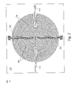
- FIG. 1 is a top view of an existing two-port CGR structure
- FIG. 2 is a top view of CGR structure with integrated electro-optical modulation, in accordance with an embodiment of the invention.
- FIG. 4 is a top view of a CGR structure with integrated electro-optical modulation, in accordance with an alternative embodiment of the invention.
- CGR circular grating resonator
- the incorporation of electrodes into a photonic structure such as a CGR is a significant challenge, since electrically conducting materials absorb light and lead to high losses.
- electrodes may be located both above and beneath the resonator (i.e., out-of-plane), such an arrangement still leads to decreased performance of the resonator.
- out-of-plane arrangement increases the complexity of the structure, as well as increases the fabrication difficulty.
- the embodiments herein introduce a CGR based electro-optical modulator based featuring in-plane electrodes. The electrodes are located at one or more nodal planes of the electric field of the particular operating resonance mode, thereby minimizing the absorption due to the electrodes.
- the electrodes will suppress all resonance modes that do not exhibit a nodal plane at the location of the electrodes.
- the CGR may also be formed with additional trenches in the circular gratings in order to suppress further unwanted resonances.
- the structure 100 includes a semiconductor substrate 102 , such as silicon dioxide (SiO 2 ), for example.
- a plurality of concentric rings 104 is formed upon the substrate 102 , the concentric rings 104 serving as Bragg mirrors and comprising a high index of refraction material such as silicon (Si), or gallium arsenide (GaAs), for example.
- Each ring 104 is spaced from one another by a region 106 of lower index material, such as air.
- the rings may be encapsulated in a cladding material such as SiO2.
- the rings 104 in FIG. 1 are shown spaced by air.
- a center disc 108 e.g., Si
- the CGR structure 100 of FIG. 1 is a two-port device, in that it also includes an input planar waveguide 110 and an output planar waveguide 112 also formed on the substrate 102 .
- Light arriving from an inward traveling mode of the input planar waveguide 110 optically couples to a grating resonator mode of the CGR, which in turn optically couples to an outward traveling mode of the output planar waveguide 112 .
- a grating resonator mode of the CGR which in turn optically couples to an outward traveling mode of the output planar waveguide 112 .
- light transmission from the input planar waveguide 110 to the second output planar waveguide 112 may be achieved.
- the two-port structure 100 can thus serve as an electro-optical modular or a spectral filter, for example.
- One way to control the refractive index of the center disc 108 is to couple an optical control signal to the center disc 108 though a separate waveguide path (not shown in FIG. 1 ) formed in the structure 100 . Additional information regarding all-optical switching with circular grating resonators may be found in U.S. Patent Application Publication 2007/0019905 of Mahrt, et al., the contents of which are incorporated herein by reference in their entirety. However, for resonators where an electrical control signal is desired, there is still the issue of how to couple electrically conductive materials to the center disc 108 in a manner that does not substantially degrade the performance of a CGR, such as the one shown in FIG. 1 .
- FIG. 2 is a top view of CGR structure 200 with integrated electro-optical modulation, in accordance with an embodiment of the invention.
- a pair of in-plane electrodes 202 , 204 is formed on the substrate 102 so as to contact opposing sides of the center disc 108 .
- trenches 206 are defined within the concentric ring pattern to accommodate the formation of the electrically conductive material of the electrodes 202 , 204 .
- a longitudinal axis of the electrode pair 202 , 204 is shown as substantially perpendicular to a longitudinal axis of the input/output planar waveguide pair 110 , 112 in the exemplary embodiment, this is actually dependent upon the location of the electric fields of the nodal planes corresponding to the resonances of the selected operating mode(s) of the resonator. That is, the location of the coplanar electrodes 202 , 204 formed on the substrate is selected so as to correspond to a region of minimum electric field intensity in the CGR, which in turn depends upon the resonance mode of the device.
- Regions 302 correspond to electric field locations of one polarity
- regions 304 correspond to electric field locations of the opposite polarity.
- the intensity of the electric field diminishes within the CGR in a radially outward direction.
- nodal planes (boundaries) for this mode of resonance are defined along the axes labeled A, B and C in FIG. 3 , along which there is substantially no electric field intensity.
- the nodal planes are disposed about 60 degrees apart from one another, with axis A being substantially perpendicular to the longitudinal axis of the input/output planar waveguide pair, within the plane of the substrate.
- the electrode pair 202 , 204 is formed at this axis (i.e., axis A in FIG. 3 ). This ensures that these “in-plane” electrical contacts do not degrade the performance of the CGR-based electro-optical modulator, since the electric field in this region is minimal and thus the placing of electrodes in this region does not lead to any additional optical absorption.
- the electrode pair 202 , 204 could also be located at either of the other two nodal planes (i.e., along axis B or along axis C), which are at an angle of about 30 degrees with respect to the longitudinal axis of the input/output planar waveguide pair.
- FIG. 4 is a top view of a CGR structure 400 with integrated electro-optical modulation, in accordance with an alternative embodiment of the invention.
- the structure 400 of FIG. 4 further includes additional trenches 402 , 404 , located at the other nodal planes corresponding to axis B and axis C in FIG. 3 .
- the embodiments described herein present a means to implement an in-plane electrical control connection for a CGR formed on a substrate.
- the electrode contacts are coplanar with respect to input and output coupling waveguides and are separated by trenches for isolation purposes.
- the angle at which the electrode contacts are disposed is dependent upon a desired operational mode, wherein the electrodes are located at nodal planes (i.e., regions of substantially no electric field intensity when the CGR is in resonance).
- This structural configuration is also easier to fabricate since no additional structures above or below the circular grating resonator are necessary.
- the in-plane electro-optical modulator also obviates the need for cladding.
Abstract
Description
Claims (5)
Priority Applications (2)
| Application Number | Priority Date | Filing Date | Title |
|---|---|---|---|
| US12/041,265 US7406226B1 (en) | 2008-03-03 | 2008-03-03 | Circular grating resonator structure with integrated electro-optical modulation |
| US12/146,601 US7474825B1 (en) | 2008-03-03 | 2008-06-26 | Circular grating resonator with integrated electro-optical modulation |
Applications Claiming Priority (1)
| Application Number | Priority Date | Filing Date | Title |
|---|---|---|---|
| US12/041,265 US7406226B1 (en) | 2008-03-03 | 2008-03-03 | Circular grating resonator structure with integrated electro-optical modulation |
Related Child Applications (1)
| Application Number | Title | Priority Date | Filing Date |
|---|---|---|---|
| US12/146,601 Continuation US7474825B1 (en) | 2008-03-03 | 2008-06-26 | Circular grating resonator with integrated electro-optical modulation |
Publications (1)
| Publication Number | Publication Date |
|---|---|
| US7406226B1 true US7406226B1 (en) | 2008-07-29 |
Family
ID=39643335
Family Applications (2)
| Application Number | Title | Priority Date | Filing Date |
|---|---|---|---|
| US12/041,265 Active US7406226B1 (en) | 2008-03-03 | 2008-03-03 | Circular grating resonator structure with integrated electro-optical modulation |
| US12/146,601 Active US7474825B1 (en) | 2008-03-03 | 2008-06-26 | Circular grating resonator with integrated electro-optical modulation |
Family Applications After (1)
| Application Number | Title | Priority Date | Filing Date |
|---|---|---|---|
| US12/146,601 Active US7474825B1 (en) | 2008-03-03 | 2008-06-26 | Circular grating resonator with integrated electro-optical modulation |
Country Status (1)
| Country | Link |
|---|---|
| US (2) | US7406226B1 (en) |
Cited By (5)
| Publication number | Priority date | Publication date | Assignee | Title |
|---|---|---|---|---|
| US20090323755A1 (en) * | 2008-06-30 | 2009-12-31 | Oki Electric Industry Co., Ltd. | Optical resonator and laser light source |
| US20190086610A1 (en) * | 2016-02-25 | 2019-03-21 | Oxford University Innovation Limited | Interferometer and method of designing an interferometer |
| US20210048726A1 (en) * | 2019-08-15 | 2021-02-18 | International Business Machines Corporation | Intracavity Grating to Suppress Single Order of Ring Resonator |
| US11262502B2 (en) * | 2020-07-16 | 2022-03-01 | Technische Universitat Dresden | Receiving device and method for determining transmission characteristics of an optical waveguide |
| CN114265146A (en) * | 2022-01-27 | 2022-04-01 | 中山大学 | Microcavity-waveguide coupling structure for realizing single photon source on chip and design method thereof |
Families Citing this family (4)
| Publication number | Priority date | Publication date | Assignee | Title |
|---|---|---|---|---|
| US8680458B2 (en) | 2010-10-07 | 2014-03-25 | Empire Technology Development, Llc | Data transmission through optical vias |
| US8682120B2 (en) | 2011-03-05 | 2014-03-25 | Alcatel Lucent | Polarization-independent grating optical coupler |
| US9162404B2 (en) * | 2011-03-05 | 2015-10-20 | Alcatel Lucent | Radial optical coupler |
| US9140854B2 (en) | 2011-09-22 | 2015-09-22 | Alcatel Lucent | Spatial division multiplexing optical mode converter |
Citations (5)
| Publication number | Priority date | Publication date | Assignee | Title |
|---|---|---|---|---|
| US3743962A (en) * | 1971-04-05 | 1973-07-03 | Bell Telephone Labor Inc | Thin film ring lasers |
| US20040247008A1 (en) * | 2003-02-12 | 2004-12-09 | Jacob Scheuer | Radial bragg ring resonator |
| US7120338B2 (en) | 2001-09-10 | 2006-10-10 | California Institute Of Technology | Tuning the index of a waveguide structure |
| US20070019905A1 (en) | 2005-06-30 | 2007-01-25 | International Business Machines Corporation | Optical switch |
| US20070201796A1 (en) | 2006-02-28 | 2007-08-30 | Gulde Stephan T | Optical structure |
Family Cites Families (1)
| Publication number | Priority date | Publication date | Assignee | Title |
|---|---|---|---|---|
| KR0132018B1 (en) * | 1994-01-27 | 1998-04-14 | 김만제 | Circle grating surface emitting laser diode |
-
2008
- 2008-03-03 US US12/041,265 patent/US7406226B1/en active Active
- 2008-06-26 US US12/146,601 patent/US7474825B1/en active Active
Patent Citations (5)
| Publication number | Priority date | Publication date | Assignee | Title |
|---|---|---|---|---|
| US3743962A (en) * | 1971-04-05 | 1973-07-03 | Bell Telephone Labor Inc | Thin film ring lasers |
| US7120338B2 (en) | 2001-09-10 | 2006-10-10 | California Institute Of Technology | Tuning the index of a waveguide structure |
| US20040247008A1 (en) * | 2003-02-12 | 2004-12-09 | Jacob Scheuer | Radial bragg ring resonator |
| US20070019905A1 (en) | 2005-06-30 | 2007-01-25 | International Business Machines Corporation | Optical switch |
| US20070201796A1 (en) | 2006-02-28 | 2007-08-30 | Gulde Stephan T | Optical structure |
Cited By (9)
| Publication number | Priority date | Publication date | Assignee | Title |
|---|---|---|---|---|
| US20090323755A1 (en) * | 2008-06-30 | 2009-12-31 | Oki Electric Industry Co., Ltd. | Optical resonator and laser light source |
| US20190086610A1 (en) * | 2016-02-25 | 2019-03-21 | Oxford University Innovation Limited | Interferometer and method of designing an interferometer |
| US10641954B2 (en) * | 2016-02-25 | 2020-05-05 | Oxford University Innovation Limited | Interferometer and method of designing an interferometer |
| US10871612B2 (en) * | 2016-02-25 | 2020-12-22 | Oxford University Innovation Limited | Interferometer and method of designing an interferometer |
| US20210048726A1 (en) * | 2019-08-15 | 2021-02-18 | International Business Machines Corporation | Intracavity Grating to Suppress Single Order of Ring Resonator |
| US10955726B2 (en) * | 2019-08-15 | 2021-03-23 | International Business Machines Corporation | Intracavity grating to suppress single order of ring resonator |
| US11294257B2 (en) | 2019-08-15 | 2022-04-05 | International Business Machines Corporation | Intracavity grating to suppress single order of ring resonator |
| US11262502B2 (en) * | 2020-07-16 | 2022-03-01 | Technische Universitat Dresden | Receiving device and method for determining transmission characteristics of an optical waveguide |
| CN114265146A (en) * | 2022-01-27 | 2022-04-01 | 中山大学 | Microcavity-waveguide coupling structure for realizing single photon source on chip and design method thereof |
Also Published As
| Publication number | Publication date |
|---|---|
| US7474825B1 (en) | 2009-01-06 |
Similar Documents
| Publication | Publication Date | Title |
|---|---|---|
| US7406226B1 (en) | Circular grating resonator structure with integrated electro-optical modulation | |
| Teng et al. | Miniaturized silicon photonics devices for integrated optical signal processors | |
| JP6198091B2 (en) | Waveguide polarization splitter and polarization rotator | |
| EP3111263B1 (en) | Apparatus and method for waveguide polarizer comprizing series of bends | |
| US6411752B1 (en) | Vertically coupled optical resonator devices over a cross-grid waveguide architecture | |
| US20150078702A1 (en) | System and Method for an Optical Phase Shifter | |
| US9696486B2 (en) | Surface-normal coupler for silicon-on-insulator platforms | |
| US8139904B2 (en) | Method and apparatus for implementing optical deflection switching using coupled resonators | |
| CN111819480B (en) | Photonic device for converting optical modes of a light beam | |
| US9122004B1 (en) | Heterogeneous resonant photonic integrated circuit | |
| CN107407776B (en) | High refractive index contrast photonic devices and applications thereof | |
| Memon et al. | Recent advances in mode converters for a mode division multiplex transmission system | |
| Sanchez et al. | Low-power operation in a silicon switch based on an asymmetric Mach–Zehnder interferometer | |
| US6614947B1 (en) | Digital optical switch using an integrated mach-zehnder interferometer having a movable phase shifter | |
| US20210116726A1 (en) | Dual-slab-layer low-loss silicon optical modulator | |
| CN111999957B (en) | Polarization insensitive photosensitive switch based on assistance of germanium antimony tellurium compound phase change material | |
| US6510259B1 (en) | Optical switch using an integrated Mach-Zehnder interferometer having a movable phase shifter and asymmetric arms | |
| Govdeli et al. | On-chip switch and add/drop multiplexer design with left-handed behavior in photonic crystals | |
| US6788837B2 (en) | Method and apparatus for interleaving and switching an optical beam in a semiconductor substrate | |
| WO2001023955A9 (en) | A nanophotonic mach-zehnder interferometer switch and filter | |
| Suzuki et al. | Polarization-Rotator-Free Polarization-Diversity 4$\times $4 Si-Wire Optical Switch | |
| Zhou et al. | Silicon large-scale optical switches using MZIs and dual-ring assisted MZIs | |
| González-Andrade et al. | Ultra-broadband mode converter and multiplexer using a sub-wavelength metamaterial | |
| Liou et al. | Investigated resonance spectrum response of ring cavity | |
| Teng | Design and characterization of optical fiber-to-chip edge couplers and on-chip mode division multiplexing devices |
Legal Events
| Date | Code | Title | Description |
|---|---|---|---|
| FEPP | Fee payment procedure |
Free format text: PAYOR NUMBER ASSIGNED (ORIGINAL EVENT CODE: ASPN); ENTITY STATUS OF PATENT OWNER: LARGE ENTITY |
|
| AS | Assignment |
Owner name: INTERNATIONAL BUSINESS MACHINES CORPORATION, NEW Y Free format text: ASSIGNMENT OF ASSIGNORS INTEREST;ASSIGNORS:HORST, FOLKERT;MOLI, NIKOLAJ;REEL/FRAME:020590/0782 Effective date: 20080229 |
|
| STCF | Information on status: patent grant |
Free format text: PATENTED CASE |
|
| REMI | Maintenance fee reminder mailed | ||
| FPAY | Fee payment |
Year of fee payment: 4 |
|
| SULP | Surcharge for late payment | ||
| AS | Assignment |
Owner name: GLOBALFOUNDRIES U.S. 2 LLC, NEW YORK Free format text: ASSIGNMENT OF ASSIGNORS INTEREST;ASSIGNOR:INTERNATIONAL BUSINESS MACHINES CORPORATION;REEL/FRAME:036550/0001 Effective date: 20150629 |
|
| AS | Assignment |
Owner name: GLOBALFOUNDRIES INC., CAYMAN ISLANDS Free format text: ASSIGNMENT OF ASSIGNORS INTEREST;ASSIGNORS:GLOBALFOUNDRIES U.S. 2 LLC;GLOBALFOUNDRIES U.S. INC.;REEL/FRAME:036779/0001 Effective date: 20150910 |
|
| FPAY | Fee payment |
Year of fee payment: 8 |
|
| AS | Assignment |
Owner name: WILMINGTON TRUST, NATIONAL ASSOCIATION, DELAWARE Free format text: SECURITY AGREEMENT;ASSIGNOR:GLOBALFOUNDRIES INC.;REEL/FRAME:049490/0001 Effective date: 20181127 |
|
| MAFP | Maintenance fee payment |
Free format text: PAYMENT OF MAINTENANCE FEE, 12TH YEAR, LARGE ENTITY (ORIGINAL EVENT CODE: M1553); ENTITY STATUS OF PATENT OWNER: LARGE ENTITY Year of fee payment: 12 |
|
| AS | Assignment |
Owner name: GLOBALFOUNDRIES U.S. INC., CALIFORNIA Free format text: ASSIGNMENT OF ASSIGNORS INTEREST;ASSIGNOR:GLOBALFOUNDRIES INC.;REEL/FRAME:054633/0001 Effective date: 20201022 |
|
| AS | Assignment |
Owner name: GLOBALFOUNDRIES INC., CAYMAN ISLANDS Free format text: RELEASE BY SECURED PARTY;ASSIGNOR:WILMINGTON TRUST, NATIONAL ASSOCIATION;REEL/FRAME:054636/0001 Effective date: 20201117 |
|
| AS | Assignment |
Owner name: GLOBALFOUNDRIES U.S. INC., NEW YORK Free format text: RELEASE BY SECURED PARTY;ASSIGNOR:WILMINGTON TRUST, NATIONAL ASSOCIATION;REEL/FRAME:056987/0001 Effective date: 20201117 |