US7420809B2 - Heat spreader in integrated circuit package - Google Patents
Heat spreader in integrated circuit package Download PDFInfo
- Publication number
- US7420809B2 US7420809B2 US10/873,387 US87338704A US7420809B2 US 7420809 B2 US7420809 B2 US 7420809B2 US 87338704 A US87338704 A US 87338704A US 7420809 B2 US7420809 B2 US 7420809B2
- Authority
- US
- United States
- Prior art keywords
- heat spreader
- die
- wire bond
- package substrate
- package
- Prior art date
- Legal status (The legal status is an assumption and is not a legal conclusion. Google has not performed a legal analysis and makes no representation as to the accuracy of the status listed.)
- Active, expires
Links
- 239000000758 substrate Substances 0.000 claims abstract description 42
- 238000000465 moulding Methods 0.000 description 11
- 229910000679 solder Inorganic materials 0.000 description 11
- DRBWRJPFNOBNIO-KOLCDFICSA-N [(2r)-1-[(2r)-2-(pyridine-4-carbonylamino)propanoyl]pyrrolidin-2-yl]boronic acid Chemical compound N([C@H](C)C(=O)N1[C@@H](CCC1)B(O)O)C(=O)C1=CC=NC=C1 DRBWRJPFNOBNIO-KOLCDFICSA-N 0.000 description 6
- 239000000463 material Substances 0.000 description 6
- 150000001875 compounds Chemical class 0.000 description 5
- RYGMFSIKBFXOCR-UHFFFAOYSA-N Copper Chemical compound [Cu] RYGMFSIKBFXOCR-UHFFFAOYSA-N 0.000 description 4
- 239000004020 conductor Substances 0.000 description 4
- 229910052802 copper Inorganic materials 0.000 description 4
- 239000010949 copper Substances 0.000 description 4
- 230000017525 heat dissipation Effects 0.000 description 4
- 238000004519 manufacturing process Methods 0.000 description 4
- 239000004593 Epoxy Substances 0.000 description 2
- 230000001070 adhesive effect Effects 0.000 description 1
- 230000002411 adverse Effects 0.000 description 1
- 230000008878 coupling Effects 0.000 description 1
- 238000010168 coupling process Methods 0.000 description 1
- 238000005859 coupling reaction Methods 0.000 description 1
- 238000005516 engineering process Methods 0.000 description 1
- 230000007613 environmental effect Effects 0.000 description 1
- 231100001261 hazardous Toxicity 0.000 description 1
- 238000003754 machining Methods 0.000 description 1
- 238000003801 milling Methods 0.000 description 1
- 238000004806 packaging method and process Methods 0.000 description 1
- 238000012536 packaging technology Methods 0.000 description 1
- 230000001681 protective effect Effects 0.000 description 1
- 230000035939 shock Effects 0.000 description 1
- 239000002470 thermal conductor Substances 0.000 description 1
Images


Classifications
-
- H—ELECTRICITY
- H01—ELECTRIC ELEMENTS
- H01L—SEMICONDUCTOR DEVICES NOT COVERED BY CLASS H10
- H01L23/00—Details of semiconductor or other solid state devices
- H01L23/34—Arrangements for cooling, heating, ventilating or temperature compensation ; Temperature sensing arrangements
- H01L23/42—Fillings or auxiliary members in containers or encapsulations selected or arranged to facilitate heating or cooling
- H01L23/433—Auxiliary members in containers characterised by their shape, e.g. pistons
- H01L23/4334—Auxiliary members in encapsulations
-
- H—ELECTRICITY
- H01—ELECTRIC ELEMENTS
- H01L—SEMICONDUCTOR DEVICES NOT COVERED BY CLASS H10
- H01L23/00—Details of semiconductor or other solid state devices
- H01L23/28—Encapsulations, e.g. encapsulating layers, coatings, e.g. for protection
- H01L23/31—Encapsulations, e.g. encapsulating layers, coatings, e.g. for protection characterised by the arrangement or shape
- H01L23/3107—Encapsulations, e.g. encapsulating layers, coatings, e.g. for protection characterised by the arrangement or shape the device being completely enclosed
- H01L23/3121—Encapsulations, e.g. encapsulating layers, coatings, e.g. for protection characterised by the arrangement or shape the device being completely enclosed a substrate forming part of the encapsulation
- H01L23/3128—Encapsulations, e.g. encapsulating layers, coatings, e.g. for protection characterised by the arrangement or shape the device being completely enclosed a substrate forming part of the encapsulation the substrate having spherical bumps for external connection
-
- H—ELECTRICITY
- H01—ELECTRIC ELEMENTS
- H01L—SEMICONDUCTOR DEVICES NOT COVERED BY CLASS H10
- H01L2224/00—Indexing scheme for arrangements for connecting or disconnecting semiconductor or solid-state bodies and methods related thereto as covered by H01L24/00
- H01L2224/01—Means for bonding being attached to, or being formed on, the surface to be connected, e.g. chip-to-package, die-attach, "first-level" interconnects; Manufacturing methods related thereto
- H01L2224/26—Layer connectors, e.g. plate connectors, solder or adhesive layers; Manufacturing methods related thereto
- H01L2224/31—Structure, shape, material or disposition of the layer connectors after the connecting process
- H01L2224/32—Structure, shape, material or disposition of the layer connectors after the connecting process of an individual layer connector
- H01L2224/321—Disposition
- H01L2224/32151—Disposition the layer connector connecting between a semiconductor or solid-state body and an item not being a semiconductor or solid-state body, e.g. chip-to-substrate, chip-to-passive
- H01L2224/32221—Disposition the layer connector connecting between a semiconductor or solid-state body and an item not being a semiconductor or solid-state body, e.g. chip-to-substrate, chip-to-passive the body and the item being stacked
- H01L2224/32225—Disposition the layer connector connecting between a semiconductor or solid-state body and an item not being a semiconductor or solid-state body, e.g. chip-to-substrate, chip-to-passive the body and the item being stacked the item being non-metallic, e.g. insulating substrate with or without metallisation
-
- H—ELECTRICITY
- H01—ELECTRIC ELEMENTS
- H01L—SEMICONDUCTOR DEVICES NOT COVERED BY CLASS H10
- H01L2224/00—Indexing scheme for arrangements for connecting or disconnecting semiconductor or solid-state bodies and methods related thereto as covered by H01L24/00
- H01L2224/01—Means for bonding being attached to, or being formed on, the surface to be connected, e.g. chip-to-package, die-attach, "first-level" interconnects; Manufacturing methods related thereto
- H01L2224/42—Wire connectors; Manufacturing methods related thereto
- H01L2224/47—Structure, shape, material or disposition of the wire connectors after the connecting process
- H01L2224/48—Structure, shape, material or disposition of the wire connectors after the connecting process of an individual wire connector
- H01L2224/4805—Shape
- H01L2224/4809—Loop shape
- H01L2224/48091—Arched
-
- H—ELECTRICITY
- H01—ELECTRIC ELEMENTS
- H01L—SEMICONDUCTOR DEVICES NOT COVERED BY CLASS H10
- H01L2224/00—Indexing scheme for arrangements for connecting or disconnecting semiconductor or solid-state bodies and methods related thereto as covered by H01L24/00
- H01L2224/01—Means for bonding being attached to, or being formed on, the surface to be connected, e.g. chip-to-package, die-attach, "first-level" interconnects; Manufacturing methods related thereto
- H01L2224/42—Wire connectors; Manufacturing methods related thereto
- H01L2224/47—Structure, shape, material or disposition of the wire connectors after the connecting process
- H01L2224/48—Structure, shape, material or disposition of the wire connectors after the connecting process of an individual wire connector
- H01L2224/481—Disposition
- H01L2224/48151—Connecting between a semiconductor or solid-state body and an item not being a semiconductor or solid-state body, e.g. chip-to-substrate, chip-to-passive
- H01L2224/48221—Connecting between a semiconductor or solid-state body and an item not being a semiconductor or solid-state body, e.g. chip-to-substrate, chip-to-passive the body and the item being stacked
- H01L2224/48225—Connecting between a semiconductor or solid-state body and an item not being a semiconductor or solid-state body, e.g. chip-to-substrate, chip-to-passive the body and the item being stacked the item being non-metallic, e.g. insulating substrate with or without metallisation
- H01L2224/48227—Connecting between a semiconductor or solid-state body and an item not being a semiconductor or solid-state body, e.g. chip-to-substrate, chip-to-passive the body and the item being stacked the item being non-metallic, e.g. insulating substrate with or without metallisation connecting the wire to a bond pad of the item
-
- H—ELECTRICITY
- H01—ELECTRIC ELEMENTS
- H01L—SEMICONDUCTOR DEVICES NOT COVERED BY CLASS H10
- H01L2224/00—Indexing scheme for arrangements for connecting or disconnecting semiconductor or solid-state bodies and methods related thereto as covered by H01L24/00
- H01L2224/73—Means for bonding being of different types provided for in two or more of groups H01L2224/10, H01L2224/18, H01L2224/26, H01L2224/34, H01L2224/42, H01L2224/50, H01L2224/63, H01L2224/71
- H01L2224/732—Location after the connecting process
- H01L2224/73251—Location after the connecting process on different surfaces
- H01L2224/73265—Layer and wire connectors
-
- H—ELECTRICITY
- H01—ELECTRIC ELEMENTS
- H01L—SEMICONDUCTOR DEVICES NOT COVERED BY CLASS H10
- H01L24/00—Arrangements for connecting or disconnecting semiconductor or solid-state bodies; Methods or apparatus related thereto
- H01L24/01—Means for bonding being attached to, or being formed on, the surface to be connected, e.g. chip-to-package, die-attach, "first-level" interconnects; Manufacturing methods related thereto
- H01L24/42—Wire connectors; Manufacturing methods related thereto
- H01L24/47—Structure, shape, material or disposition of the wire connectors after the connecting process
- H01L24/48—Structure, shape, material or disposition of the wire connectors after the connecting process of an individual wire connector
-
- H—ELECTRICITY
- H01—ELECTRIC ELEMENTS
- H01L—SEMICONDUCTOR DEVICES NOT COVERED BY CLASS H10
- H01L24/00—Arrangements for connecting or disconnecting semiconductor or solid-state bodies; Methods or apparatus related thereto
- H01L24/73—Means for bonding being of different types provided for in two or more of groups H01L24/10, H01L24/18, H01L24/26, H01L24/34, H01L24/42, H01L24/50, H01L24/63, H01L24/71
-
- H—ELECTRICITY
- H01—ELECTRIC ELEMENTS
- H01L—SEMICONDUCTOR DEVICES NOT COVERED BY CLASS H10
- H01L2924/00—Indexing scheme for arrangements or methods for connecting or disconnecting semiconductor or solid-state bodies as covered by H01L24/00
- H01L2924/0001—Technical content checked by a classifier
- H01L2924/00014—Technical content checked by a classifier the subject-matter covered by the group, the symbol of which is combined with the symbol of this group, being disclosed without further technical details
-
- H—ELECTRICITY
- H01—ELECTRIC ELEMENTS
- H01L—SEMICONDUCTOR DEVICES NOT COVERED BY CLASS H10
- H01L2924/00—Indexing scheme for arrangements or methods for connecting or disconnecting semiconductor or solid-state bodies as covered by H01L24/00
- H01L2924/10—Details of semiconductor or other solid state devices to be connected
- H01L2924/11—Device type
- H01L2924/14—Integrated circuits
-
- H—ELECTRICITY
- H01—ELECTRIC ELEMENTS
- H01L—SEMICONDUCTOR DEVICES NOT COVERED BY CLASS H10
- H01L2924/00—Indexing scheme for arrangements or methods for connecting or disconnecting semiconductor or solid-state bodies as covered by H01L24/00
- H01L2924/15—Details of package parts other than the semiconductor or other solid state devices to be connected
- H01L2924/151—Die mounting substrate
- H01L2924/153—Connection portion
- H01L2924/1531—Connection portion the connection portion being formed only on the surface of the substrate opposite to the die mounting surface
- H01L2924/15311—Connection portion the connection portion being formed only on the surface of the substrate opposite to the die mounting surface being a ball array, e.g. BGA
-
- H—ELECTRICITY
- H01—ELECTRIC ELEMENTS
- H01L—SEMICONDUCTOR DEVICES NOT COVERED BY CLASS H10
- H01L2924/00—Indexing scheme for arrangements or methods for connecting or disconnecting semiconductor or solid-state bodies as covered by H01L24/00
- H01L2924/15—Details of package parts other than the semiconductor or other solid state devices to be connected
- H01L2924/161—Cap
- H01L2924/1615—Shape
- H01L2924/16152—Cap comprising a cavity for hosting the device, e.g. U-shaped cap
Definitions
- Integrated circuits are generally formed in a “package” that has electrical connections (e.g. leads, pins, balls, etc.) between an IC die inside the package and the outside of the package.
- the IC die must be protected to prevent damage to it, so the IC die is commonly surrounded by a material that is highly impervious to air, moisture, shock and other potentially hazardous environmental conditions.
- the protective material is also commonly a poor thermal conductor, so to improve heat dissipation from the IC die, a heat spreader (commonly called a “drop-in heat spreader”) is included in the IC package to transfer heat from the IC die to the surrounding environment.
- the heat spreader may also be used to attenuate EMI emissions from the IC package.
- FIGS. 1 and 2 A prior art heat spreader 100 is shown in FIGS. 1 and 2 .
- the heat spreader 100 is shown in cross section (at section 2 - 2 in FIG. 1 ) as part of an IC package 102 .
- the IC package 102 also includes an IC die 104 , a substrate 106 , several wire bonds 108 , a molding compound 110 and several solder balls 112 (e.g. for a ball grid array, “BGA”).
- the heat spreader 100 is mounted on the substrate 106 to cover the IC die 104 and the wire bonds 108 .
- the heat spreader 100 has a raised circular portion 114 that surrounds the IC die 104 and the wire bonds 108 .
- the heat spreader 100 also has dimples 116 that are electrically connected to the substrate 106 to ground the heat spreader 100 for EMI attenuation purposes.
- Heat from the IC die 104 generally radiates through the molding compound 110 to the heat spreader 100 as well as through the substrate 106 . From the heat spreader 100 and the substrate 106 the heat is dissipated to the environment. It is preferable that most of the heat dissipates through the heat spreader 100 , because the substrate 106 may have components, such as the solder balls 112 , that are vulnerable to heat.
- the amount of heat that can be dissipated by the heat spreader 100 instead of through any other part of the IC package 102 , largely depends on the thermal conductive properties of the molding compound 110 (e.g. a higher thermal conductivity is better for this consideration) and the distance between the heat spreader 100 and the source of the heat, i.e. the IC die 104 (e.g. a closer distance is better for this consideration).
- the molding compound 110 is selected not for its thermal conductive properties, but rather for a variety of other important characteristics. As a result, the molding compound 110 commonly has poor thermal conductive properties. Additionally, the distance between the heat spreader 100 and the IC die 104 is limited by clearance requirements for the loops of the wire bonds 108 .
- the problem of the distance between the heat spreader 100 and the IC die 104 is further exacerbated by a continuing trend in IC packaging technologies to increase the number and/or density of the BGA solder balls 112 .
- the prior art example shown in FIG. 2 includes three rows of I/O (input/output) pads 118 along each edge of the IC die 104 .
- I/O input/output
- IC dies having four or five, or more, rows are being developed.
- the wire bonds 108 that connect to the inner rows of I/O pads 118 have to extend with sufficient clearance over the wire bonds 108 that connect to the outer rows of I/O pads 118 .
- the wire bonds 108 for the innermost row will have to extend higher to properly pass over the wire bonds 108 of the other rows.
- the distance between the heat spreader 100 and the IC die 104 will have to be increased.
- the increased distance between the heat spreader 100 and the IC die 104 will decrease the efficiency with which the heat spreader 100 can dissipate the heat from the IC die 104 .
- costly new manufacturing tools will have to be developed to handle the IC packages 102 having a greater height dimension.
- An improved IC package and heat spreader that overcomes the problems discussed above incorporates an opening, or hole, in the heat spreader, preferably near a point where the wire bonds reach a maximum height or distance above the IC die or the package substrate.
- the opening provides an additional space for the wire bonds to extend into without requiring additional height for the heat spreader.
- the heat spreader and the overall height of the IC package allow use of many of the same manufacturing tools used to make the prior art IC packages.
- the heat spreader preferably surrounds, instead of covers, the portion of the wire bonds within the opening, so the distance between the improved heat spreader and the IC die is not constrained by the maximum height of the wire bonds. Therefore, the improved heat spreader preferably has a thickness that extends the heat spreader to within a minimum clearance of the IC die, so the heat dissipation efficiency of the improved heat spreader is greater than that of the prior art heat spreader.
- a side of the improved heat spreader can be made substantially parallel and close to a portion of the length of the wire bonds. In this manner, the improved heat spreader can attenuate EMI emissions from the wire bonds more efficiently than can the prior art heat spreader.
- FIG. 1 is a plan view of a prior art drop-in heat spreader for an IC package.
- FIG. 2 is a side cross sectional view of the prior art heat spreader shown in FIG. 1 and incorporated in an IC package.
- FIG. 3 is a plan view of a heat spreader incorporating an embodiment of the present invention.
- FIG. 4 is a side cross sectional view of the heat spreader shown in FIG. 3 .
- FIG. 5 is a cut away perspective view of the heat spreader shown in FIG. 3 .
- FIG. 6 is a plan view of an IC package incorporating the heat spreader shown in FIG. 3 .
- FIG. 7 is a side cross sectional view of the IC package shown in FIG. 6 .
- FIG. 8 is another plan view of the IC package shown in FIG. 6 .
- FIG. 9 is a cut away perspective view of an alternative embodiment of a heat spreader incorporating the present invention.
- FIG. 10 is a plan view of another alternative embodiment of a heat spreader incorporating the present invention.
- FIGS. 3 , 4 and 5 A drop-in heat spreader 200 incorporating an embodiment of the present invention and providing improved electrical and thermal characteristics when incorporated in an integrated circuit (IC) package (described below) is shown in FIGS. 3 , 4 and 5 .
- IC integrated circuit
- FIGS. 3 , 4 and 5 A drop-in heat spreader 200 incorporating an embodiment of the present invention and providing improved electrical and thermal characteristics when incorporated in an integrated circuit (IC) package (described below) is shown in FIGS. 3 , 4 and 5 .
- IC integrated circuit
- the heat spreader 200 generally includes one or more openings, or elongated holes, 202 in an upper portion 204 thereof, as shown in FIGS. 3 , 4 and 5 .
- the heat spreader 200 also generally includes a lower portion 206 for mounting or connecting to an IC (integrated circuit) package substrate as will be described below.
- the upper portion 204 generally includes a central portion 208 and an outer portion 210 connected by bridges 212 .
- the outer portion 210 is connected to the lower portion 206 .
- the outer portion 210 preferably has a sloping under side 214 ( FIGS. 4 and 5 ).
- the portions 204 , 206 , 208 , 210 and 212 are preferably formed integrally together, but may be separate components joined together.
- the lower portion 206 is generally square or rectangular, as shown in FIGS. 3 and 5 , but may be of any appropriate shape for the IC package into which the heat spreader 200 is to be incorporated.
- the upper portion 204 is generally circular, as shown in FIGS. 3 and 5 , but may be of any appropriate shape.
- the openings 202 preferably have a trapezoidal shape with a convex curved long edge 216 , as shown, but may be of any appropriate shape, as will be described below.
- the heat spreader 200 is preferably for use in an IC package 218 , as shown in FIGS. 6 , 7 and 8 .
- the IC package 218 generally includes a package substrate 220 ( FIGS. 6 , 7 and 8 ), an IC die 222 ( FIGS. 7 and 8 ), several wire bonds 224 ( FIGS. 7 and 8 ) and a molding compound 226 ( FIG. 7 ).
- the IC package 218 also has several I/O points, such as solder balls 228 ( FIGS. 6 and 7 ) for a ball grid array (BGA) type of I/O system.
- BGA ball grid array
- the heat spreader 200 is preferably made of copper, but may be made of any appropriate thermally conductive material.
- a top surface 229 of the upper portion 204 of the heat spreader 200 is typically nickel-plated.
- the bottom of the heat spreader 200 is typically oxidized for form a black oxide, which provides adhesive properties with the molding compound 226 .
- the molding compound 226 preferably completely fills in the volume between the heat spreader 200 and the package substrate 220 .
- the nickel-plated portion is preferably visible.
- the heat spreader is embedded in the molding compound 226 .
- Molding compound 226 is preferably a black epoxy material.
- the IC die 222 is connected to the package substrate 220 at a die attach pad, or paddle, 230 ( FIG. 7 ) by a die attach epoxy 232 .
- a solder mask 234 separates the IC die 222 from the die attach pad 230 .
- the IC die 222 may also be electrically connected by vias (not shown) to the die attach pad 230 (e.g. for electrical grounding to the package substrate 220 ).
- the die attach pad 230 is preferably a copper layer.
- the IC die 222 generally includes rows of I/O pads 236 ( FIGS. 7 and 8 ).
- the 110 pads 236 of one row are generally staggered relative to the I/O pads of the next adjacent row, as shown in FIG. 8 .
- the number of I/O pads 236 on the IC die 222 depends on the number of I/O circuits of the IC die 222 .
- the package substrate 220 generally includes bond pads, “fingers” or “rings” 238 (e.g. copper or other conductor).
- the I/O pads 236 of the IC die 222 are electrically connected by the wire bonds 224 to the bond pads 238 of the package substrate 220 .
- the package substrate 220 also generally includes connection pads 240 (e.g.
- the solder balls 228 are electrically connected to the package substrate 220 at the connection pads 240 .
- the package substrate 220 is typically a laminated multi-layered board having several vias (not shown) and several layers of conductive traces (not shown) disposed therein to electrically connect the bond pads 236 to the solder balls 228 .
- the heat spreader 200 preferably also includes dimples 244 ( FIGS. 3 , 4 and 6 - 8 ) on the lower portion 206 .
- the package substrate 220 preferably includes a copper layer 246 covered by a solder mask 248 .
- the dimples 244 contact the copper layer 246 through a hole in the solder mask 248 .
- the heat spreader 200 is, thus, electrically connected to the package substrate 220 at the dimples 244 in order to ground the heat spreader 200 for attenuation of EMI emissions from the IC die 222 and particularly the wire bonds 224 .
- the wire bonds 224 of the inner rows of I/O pads 236 (as seen in FIG. 7 ) preferably extend upward into the openings 202 between the central portion 208 and the outer portion 210 , loop over the wire bonds 224 of the outer rows and extend back down to the bond pads 238 .
- the wire bonds 224 of the innermost row preferably extend to a maximum distance point 250 from the IC die 222 or the package substrate 220 .
- the openings 202 enable the maximum distance point 250 of the wire bonds 224 to be greater than that for the prior art IC packages 102 ( FIG. 2 ) without increasing the height of the heat spreader 200 .
- the openings 202 allow more rows of the I/O pads 236 on the IC die 222 and, likewise, more I/O pads 236 in general without an increase in the size of the heat spreader 200 or of the IC package 218 . Therefore, it is possible to use the same tools and machines for manufacturing the IC package 218 as for the prior art IC package 102 .
- the wire bonds 224 preferably slope downward substantially parallel to the sloping under side 214 of the outer portion 210 of the upper portion 204 of the heat spreader 200 . Additionally, the clearance between the wire bonds 224 and the sloping under side 214 is preferably a minimum. In this manner, the EMI attenuation capability of the heat spreader 200 is optimized, or maximized, to reduce electrical coupling or crosstalk between the signals carried by the wire bonds 224 .
- the central portion 208 preferably covers a substantial portion of the IC die 222 (as seen in FIG. 8 ).
- the only portion of the IC die 222 that is preferably not covered by the central portion 208 is near the edges of the IC die 222 , including most, if not all, of the I/O pads 236 .
- the corners of the IC die 222 may be covered by the bridges 212 .
- the central portion 208 of the upper portion 204 of the heat spreader 200 preferably has a thickness that extends down close to the IC die 222 (as seen in FIG. 7 ). This thickness may be substantially greater than the thickness of the prior art heat spreader 100 ( FIGS. 1 and 2 ).
- the bottom side of the central portion 208 is preferably separated from the top surface of the IC die 222 by a minimum clearance distance. The clearance distance is minimized by determining the closest distance that the bottom side of the central portion 208 can be to the IC die 222 without touching it or adversely affecting its function.
- the heat dissipation efficiency of the heat spreader 200 may be optimized, or maximized, since the heat has the smallest amount of the molding compound 226 (typically a poor heat conductor) through which to pass to reach the heat spreader 200 , where the heat can be more rapidly dissipated.
- An exemplary minimum clearance distance may be about five mils.
- the bridges 212 are preferably made as thick as the central portion 208 .
- Fabrication of the heat spreader 200 preferably starts with a rectangular piece of the desired material of uniform thickness.
- the rectangular piece of material is then preferably stamped to the desired shape, including the openings 202 .
- Some machining, or milling, of the heat spreader 200 may be needed to create the non-uniform thickness of the outer portion 210 .
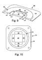
- FIG. 9 A heat spreader 300 incorporating an alternative embodiment of the present invention is shown in FIG. 9 .
- the heat spreader 300 generally includes an upper portion 302 and a lower portion 304 .
- the upper portion 302 preferably includes openings 306 (e.g. similar to the openings 202 , FIGS. 3-8 ) between a central portion 308 and an outer portion 310 .
- the central portion 308 and the outer portion 310 are preferably formed with almost vertical upper sidewalls 312 at the openings 306 and lower sidewalls 314 that slope away from the openings 306 .
- FIG. 10 A heat spreader 316 incorporating an alternative embodiment of the present invention is shown in FIG. 10 .
- the heat spreader 316 generally includes an upper portion 318 and a lower portion 320 .
- the upper portion 318 preferably includes openings 322 between a central portion 324 and an outer portion 326 .
- the openings 322 are preferably rectangular or rounded-rectangular (as shown) in shape.
Abstract
Description
Claims (15)
Priority Applications (1)
| Application Number | Priority Date | Filing Date | Title |
|---|---|---|---|
| US10/873,387 US7420809B2 (en) | 2004-06-22 | 2004-06-22 | Heat spreader in integrated circuit package |
Applications Claiming Priority (1)
| Application Number | Priority Date | Filing Date | Title |
|---|---|---|---|
| US10/873,387 US7420809B2 (en) | 2004-06-22 | 2004-06-22 | Heat spreader in integrated circuit package |
Publications (2)
| Publication Number | Publication Date |
|---|---|
| US20050281011A1 US20050281011A1 (en) | 2005-12-22 |
| US7420809B2 true US7420809B2 (en) | 2008-09-02 |
Family
ID=35480340
Family Applications (1)
| Application Number | Title | Priority Date | Filing Date |
|---|---|---|---|
| US10/873,387 Active 2024-10-13 US7420809B2 (en) | 2004-06-22 | 2004-06-22 | Heat spreader in integrated circuit package |
Country Status (1)
| Country | Link |
|---|---|
| US (1) | US7420809B2 (en) |
Cited By (20)
| Publication number | Priority date | Publication date | Assignee | Title |
|---|---|---|---|---|
| US20090207525A1 (en) * | 2004-04-06 | 2009-08-20 | Headway Technologies, Inc. | Perpendicular write head with tapered main pole |
| US20090315192A1 (en) * | 2008-06-24 | 2009-12-24 | Elpida Memory, Inc. | Method of manufacturing semiconductor device and semiconductor device |
| US7825520B1 (en) | 2006-11-16 | 2010-11-02 | Amkor Technology, Inc. | Stacked redistribution layer (RDL) die assembly package |
| US20110085304A1 (en) * | 2009-10-14 | 2011-04-14 | Irvine Sensors Corporation | Thermal management device comprising thermally conductive heat spreader with electrically isolated through-hole vias |
| US7960827B1 (en) * | 2009-04-09 | 2011-06-14 | Amkor Technology, Inc. | Thermal via heat spreader package and method |
| US8018068B1 (en) | 2004-03-23 | 2011-09-13 | Amkor Technology, Inc. | Semiconductor package including a top-surface metal layer for implementing circuit features |
| US8026587B1 (en) | 2002-05-01 | 2011-09-27 | Amkor Technology, Inc. | Semiconductor package including top-surface terminals for mounting another semiconductor package |
| US8337657B1 (en) | 2010-10-27 | 2012-12-25 | Amkor Technology, Inc. | Mechanical tape separation package and method |
| US8341835B1 (en) | 2002-05-01 | 2013-01-01 | Amkor Technology, Inc. | Buildup dielectric layer having metallization pattern semiconductor package fabrication method |
| US8535961B1 (en) | 2010-12-09 | 2013-09-17 | Amkor Technology, Inc. | Light emitting diode (LED) package and method |
| US8653674B1 (en) | 2011-09-15 | 2014-02-18 | Amkor Technology, Inc. | Electronic component package fabrication method and structure |
| US8890329B2 (en) | 2011-04-26 | 2014-11-18 | Amkor Technology, Inc. | Semiconductor device |
| US9013011B1 (en) | 2011-03-11 | 2015-04-21 | Amkor Technology, Inc. | Stacked and staggered die MEMS package and method |
| US9064838B2 (en) | 2013-09-17 | 2015-06-23 | Freescale Semiconductor, Inc. | Heat spreader for integrated circuit device |
| US9385060B1 (en) | 2014-07-25 | 2016-07-05 | Altera Corporation | Integrated circuit package with enhanced thermal conduction |
| US9691635B1 (en) | 2002-05-01 | 2017-06-27 | Amkor Technology, Inc. | Buildup dielectric layer having metallization pattern semiconductor package fabrication method |
| US9704747B2 (en) | 2013-03-29 | 2017-07-11 | Amkor Technology, Inc. | Semiconductor device and manufacturing method thereof |
| US9748154B1 (en) | 2010-11-04 | 2017-08-29 | Amkor Technology, Inc. | Wafer level fan out semiconductor device and manufacturing method thereof |
| US10811277B2 (en) | 2004-03-23 | 2020-10-20 | Amkor Technology, Inc. | Encapsulated semiconductor package |
| US11081370B2 (en) | 2004-03-23 | 2021-08-03 | Amkor Technology Singapore Holding Pte. Ltd. | Methods of manufacturing an encapsulated semiconductor device |
Families Citing this family (1)
| Publication number | Priority date | Publication date | Assignee | Title |
|---|---|---|---|---|
| JP2018182195A (en) * | 2017-04-19 | 2018-11-15 | トヨタ自動車株式会社 | Semiconductor device |
Citations (18)
| Publication number | Priority date | Publication date | Assignee | Title |
|---|---|---|---|---|
| US5397917A (en) * | 1993-04-26 | 1995-03-14 | Motorola, Inc. | Semiconductor package capable of spreading heat |
| US5473512A (en) * | 1993-12-16 | 1995-12-05 | At&T Corp. | Electronic device package having electronic device boonded, at a localized region thereof, to circuit board |
| US5485037A (en) * | 1993-04-12 | 1996-01-16 | Amkor Electronics, Inc. | Semiconductor device having a thermal dissipator and electromagnetic shielding |
| US5641987A (en) * | 1994-06-21 | 1997-06-24 | Anam Industrial Co., Ltd. | Heat spreader suitable for use in semiconductor packages having different pad sizes |
| US5691567A (en) * | 1995-09-19 | 1997-11-25 | National Semiconductor Corporation | Structure for attaching a lead frame to a heat spreader/heat slug structure |
| US5872395A (en) * | 1996-09-16 | 1999-02-16 | International Packaging And Assembly Corporation | Bent tip method for preventing vertical motion of heat spreaders during injection molding of IC packages |
| US5909057A (en) * | 1997-09-23 | 1999-06-01 | Lsi Logic Corporation | Integrated heat spreader/stiffener with apertures for semiconductor package |
| US5977626A (en) * | 1998-08-12 | 1999-11-02 | Industrial Technology Research Institute | Thermally and electrically enhanced PBGA package |
| US5982621A (en) * | 1998-11-23 | 1999-11-09 | Caesar Technology Inc. | Electronic device cooling arrangement |
| US6278613B1 (en) * | 2000-09-27 | 2001-08-21 | St Assembly Test Services Pte Ltd | Copper pads for heat spreader attach |
| US6472741B1 (en) * | 2001-07-14 | 2002-10-29 | Siliconware Precision Industries Co., Ltd. | Thermally-enhanced stacked-die ball grid array semiconductor package and method of fabricating the same |
| US6534859B1 (en) * | 2002-04-05 | 2003-03-18 | St. Assembly Test Services Ltd. | Semiconductor package having heat sink attached to pre-molded cavities and method for creating the package |
| US6541854B2 (en) * | 2000-12-01 | 2003-04-01 | Siliconware Precision Industries Co., Ltd. | Super low profile package with high efficiency of heat dissipation |
| US6552428B1 (en) * | 1998-10-12 | 2003-04-22 | Siliconware Precision Industries Co., Ltd. | Semiconductor package having an exposed heat spreader |
| US6707168B1 (en) * | 2001-05-04 | 2004-03-16 | Amkor Technology, Inc. | Shielded semiconductor package with single-sided substrate and method for making the same |
| US6720649B2 (en) * | 2001-12-07 | 2004-04-13 | Siliconware Precision Industries Co., Ltd. | Semiconductor package with heat dissipating structure |
| US6750534B2 (en) * | 2000-08-14 | 2004-06-15 | St Assembly Test Services Ltd | Heat spreader hole pin 1 identifier |
| US6882041B1 (en) * | 2002-02-05 | 2005-04-19 | Altera Corporation | Thermally enhanced metal capped BGA package |
-
2004
- 2004-06-22 US US10/873,387 patent/US7420809B2/en active Active
Patent Citations (18)
| Publication number | Priority date | Publication date | Assignee | Title |
|---|---|---|---|---|
| US5485037A (en) * | 1993-04-12 | 1996-01-16 | Amkor Electronics, Inc. | Semiconductor device having a thermal dissipator and electromagnetic shielding |
| US5397917A (en) * | 1993-04-26 | 1995-03-14 | Motorola, Inc. | Semiconductor package capable of spreading heat |
| US5473512A (en) * | 1993-12-16 | 1995-12-05 | At&T Corp. | Electronic device package having electronic device boonded, at a localized region thereof, to circuit board |
| US5641987A (en) * | 1994-06-21 | 1997-06-24 | Anam Industrial Co., Ltd. | Heat spreader suitable for use in semiconductor packages having different pad sizes |
| US5691567A (en) * | 1995-09-19 | 1997-11-25 | National Semiconductor Corporation | Structure for attaching a lead frame to a heat spreader/heat slug structure |
| US5872395A (en) * | 1996-09-16 | 1999-02-16 | International Packaging And Assembly Corporation | Bent tip method for preventing vertical motion of heat spreaders during injection molding of IC packages |
| US5909057A (en) * | 1997-09-23 | 1999-06-01 | Lsi Logic Corporation | Integrated heat spreader/stiffener with apertures for semiconductor package |
| US5977626A (en) * | 1998-08-12 | 1999-11-02 | Industrial Technology Research Institute | Thermally and electrically enhanced PBGA package |
| US6552428B1 (en) * | 1998-10-12 | 2003-04-22 | Siliconware Precision Industries Co., Ltd. | Semiconductor package having an exposed heat spreader |
| US5982621A (en) * | 1998-11-23 | 1999-11-09 | Caesar Technology Inc. | Electronic device cooling arrangement |
| US6750534B2 (en) * | 2000-08-14 | 2004-06-15 | St Assembly Test Services Ltd | Heat spreader hole pin 1 identifier |
| US6278613B1 (en) * | 2000-09-27 | 2001-08-21 | St Assembly Test Services Pte Ltd | Copper pads for heat spreader attach |
| US6541854B2 (en) * | 2000-12-01 | 2003-04-01 | Siliconware Precision Industries Co., Ltd. | Super low profile package with high efficiency of heat dissipation |
| US6707168B1 (en) * | 2001-05-04 | 2004-03-16 | Amkor Technology, Inc. | Shielded semiconductor package with single-sided substrate and method for making the same |
| US6472741B1 (en) * | 2001-07-14 | 2002-10-29 | Siliconware Precision Industries Co., Ltd. | Thermally-enhanced stacked-die ball grid array semiconductor package and method of fabricating the same |
| US6720649B2 (en) * | 2001-12-07 | 2004-04-13 | Siliconware Precision Industries Co., Ltd. | Semiconductor package with heat dissipating structure |
| US6882041B1 (en) * | 2002-02-05 | 2005-04-19 | Altera Corporation | Thermally enhanced metal capped BGA package |
| US6534859B1 (en) * | 2002-04-05 | 2003-03-18 | St. Assembly Test Services Ltd. | Semiconductor package having heat sink attached to pre-molded cavities and method for creating the package |
Non-Patent Citations (3)
| Title |
|---|
| "STATS-DQFP Cross Section Drawing," ST Assembly Test Services, Ltd., http://www.stts.com/stts/pages/page.asp?SID=3&PageID=102, 2004, p. 1. |
| Bruce M. Guenin, Ph.D., "Packaging: designing for thermal performance," Cooling Zone, ElectronicsCooling Online, http://www.coolingzone.com/Content/Library/Papers/May%201997/Article%2001/May%201997<SUB>-</SUB>01.html, (C) 1995-2000 , p. 1-7. |
| Milton L. Buschbom, Mark Peterson, Shih-Fang Chuang, David Kee, and Buford Carter, "Thermally Enhanced ICs: Low Cost Plastic Package Improves Surface-Mount IC Cooling," PCIM, Nov. 1998, p. 1-7. |
Cited By (33)
| Publication number | Priority date | Publication date | Assignee | Title |
|---|---|---|---|---|
| US8026587B1 (en) | 2002-05-01 | 2011-09-27 | Amkor Technology, Inc. | Semiconductor package including top-surface terminals for mounting another semiconductor package |
| US9812386B1 (en) | 2002-05-01 | 2017-11-07 | Amkor Technology, Inc. | Encapsulated semiconductor package |
| US10461006B1 (en) | 2002-05-01 | 2019-10-29 | Amkor Technology, Inc. | Encapsulated semiconductor package |
| US8341835B1 (en) | 2002-05-01 | 2013-01-01 | Amkor Technology, Inc. | Buildup dielectric layer having metallization pattern semiconductor package fabrication method |
| US9691635B1 (en) | 2002-05-01 | 2017-06-27 | Amkor Technology, Inc. | Buildup dielectric layer having metallization pattern semiconductor package fabrication method |
| US8110909B1 (en) | 2002-05-01 | 2012-02-07 | Amkor Technology, Inc. | Semiconductor package including top-surface terminals for mounting another semiconductor package |
| US8227338B1 (en) | 2004-03-23 | 2012-07-24 | Amkor Technology, Inc. | Semiconductor package including a top-surface metal layer for implementing circuit features |
| US11094560B1 (en) | 2004-03-23 | 2021-08-17 | Amkor Technology Singapore Holding Pte. Ltd. | Encapsulated semiconductor package |
| US10811277B2 (en) | 2004-03-23 | 2020-10-20 | Amkor Technology, Inc. | Encapsulated semiconductor package |
| US8018068B1 (en) | 2004-03-23 | 2011-09-13 | Amkor Technology, Inc. | Semiconductor package including a top-surface metal layer for implementing circuit features |
| US11081370B2 (en) | 2004-03-23 | 2021-08-03 | Amkor Technology Singapore Holding Pte. Ltd. | Methods of manufacturing an encapsulated semiconductor device |
| US20090207525A1 (en) * | 2004-04-06 | 2009-08-20 | Headway Technologies, Inc. | Perpendicular write head with tapered main pole |
| US11848214B2 (en) | 2006-08-01 | 2023-12-19 | Amkor Technology Singapore Holding Pte. Ltd. | Encapsulated semiconductor package |
| US8629546B1 (en) | 2006-11-16 | 2014-01-14 | Amkor Technology, Inc. | Stacked redistribution layer (RDL) die assembly package |
| US8203203B1 (en) | 2006-11-16 | 2012-06-19 | Amkor Technology, Inc. | Stacked redistribution layer (RDL) die assembly package |
| US7825520B1 (en) | 2006-11-16 | 2010-11-02 | Amkor Technology, Inc. | Stacked redistribution layer (RDL) die assembly package |
| US8169089B2 (en) * | 2008-06-24 | 2012-05-01 | Elpida Memory, Inc. | Semiconductor device including semiconductor chip and sealing material |
| US20090315192A1 (en) * | 2008-06-24 | 2009-12-24 | Elpida Memory, Inc. | Method of manufacturing semiconductor device and semiconductor device |
| US7960827B1 (en) * | 2009-04-09 | 2011-06-14 | Amkor Technology, Inc. | Thermal via heat spreader package and method |
| US20110085304A1 (en) * | 2009-10-14 | 2011-04-14 | Irvine Sensors Corporation | Thermal management device comprising thermally conductive heat spreader with electrically isolated through-hole vias |
| US8753730B1 (en) | 2010-10-27 | 2014-06-17 | Amkor Technology, Inc. | Mechanical tape separation package |
| US8337657B1 (en) | 2010-10-27 | 2012-12-25 | Amkor Technology, Inc. | Mechanical tape separation package and method |
| US9748154B1 (en) | 2010-11-04 | 2017-08-29 | Amkor Technology, Inc. | Wafer level fan out semiconductor device and manufacturing method thereof |
| US10903181B2 (en) | 2010-11-04 | 2021-01-26 | Amkor Technology Singapore Holding Pte. Ltd. | Wafer level fan out semiconductor device and manufacturing method thereof |
| US11855023B2 (en) | 2010-11-04 | 2023-12-26 | Amkor Technology Singapore Holding Pte. Ltd. | Wafer level fan out semiconductor device and manufacturing method thereof |
| US8535961B1 (en) | 2010-12-09 | 2013-09-17 | Amkor Technology, Inc. | Light emitting diode (LED) package and method |
| US9013011B1 (en) | 2011-03-11 | 2015-04-21 | Amkor Technology, Inc. | Stacked and staggered die MEMS package and method |
| US8890329B2 (en) | 2011-04-26 | 2014-11-18 | Amkor Technology, Inc. | Semiconductor device |
| US8941250B1 (en) | 2011-09-15 | 2015-01-27 | Amkor Technology, Inc. | Electronic component package fabrication method and structure |
| US8653674B1 (en) | 2011-09-15 | 2014-02-18 | Amkor Technology, Inc. | Electronic component package fabrication method and structure |
| US9704747B2 (en) | 2013-03-29 | 2017-07-11 | Amkor Technology, Inc. | Semiconductor device and manufacturing method thereof |
| US9064838B2 (en) | 2013-09-17 | 2015-06-23 | Freescale Semiconductor, Inc. | Heat spreader for integrated circuit device |
| US9385060B1 (en) | 2014-07-25 | 2016-07-05 | Altera Corporation | Integrated circuit package with enhanced thermal conduction |
Also Published As
| Publication number | Publication date |
|---|---|
| US20050281011A1 (en) | 2005-12-22 |
Similar Documents
| Publication | Publication Date | Title |
|---|---|---|
| US7420809B2 (en) | Heat spreader in integrated circuit package | |
| US6657296B2 (en) | Semicondctor package | |
| JP4437919B2 (en) | EMI shielding for electronic parts package | |
| US6359341B1 (en) | Ball grid array integrated circuit package structure | |
| US7402906B2 (en) | Enhanced die-down ball grid array and method for making the same | |
| US7126218B1 (en) | Embedded heat spreader ball grid array | |
| US6229702B1 (en) | Ball grid array semiconductor package having improved heat dissipation efficiency, overall electrical performance and enhanced bonding capability | |
| US7317247B2 (en) | Semiconductor package having heat spreader and package stack using the same | |
| US6515870B1 (en) | Package integrated faraday cage to reduce electromagnetic emissions from an integrated circuit | |
| USRE42653E1 (en) | Semiconductor package with heat dissipating structure | |
| US7034388B2 (en) | Stack type flip-chip package | |
| KR100899314B1 (en) | Semiconductor device and method of manufacturing the same | |
| US6818978B1 (en) | Ball grid array package with shielding | |
| US9484282B2 (en) | Resin-sealed semiconductor device | |
| US8018037B2 (en) | Semiconductor chip package | |
| US20070069371A1 (en) | Cavity chip package | |
| US20020096767A1 (en) | Cavity down ball grid array package with EMI shielding and reduced thermal resistance | |
| US6933602B1 (en) | Semiconductor package having a thermally and electrically connected heatspreader | |
| US6255140B1 (en) | Flip chip chip-scale package | |
| US20070205495A1 (en) | Electronic Component With Stacked Semiconductor Chips And Heat Dissipating Means | |
| US20040183180A1 (en) | Multi-chips stacked package | |
| US6130477A (en) | Thin enhanced TAB BGA package having improved heat dissipation | |
| US20060202335A1 (en) | Tape ball grid array package with electromagnetic interference protection and method for fabricating the package | |
| KR20060039044A (en) | Stack type semiconductor multi-chip package | |
| US7235889B2 (en) | Integrated heatspreader for use in wire bonded ball grid array semiconductor packages |
Legal Events
| Date | Code | Title | Description |
|---|---|---|---|
| AS | Assignment |
Owner name: LSI LOGIC CORPORATION, CALIFORNIA Free format text: ASSIGNMENT OF ASSIGNORS INTEREST;ASSIGNORS:LIM, HONG T.;OTHIENO, MAURICE O.;LOW, QWAI H.;REEL/FRAME:015512/0723 Effective date: 20040621 |
|
| FEPP | Fee payment procedure |
Free format text: PAYOR NUMBER ASSIGNED (ORIGINAL EVENT CODE: ASPN); ENTITY STATUS OF PATENT OWNER: LARGE ENTITY |
|
| AS | Assignment |
Owner name: LSI CORPORATION, CALIFORNIA Free format text: MERGER;ASSIGNOR:LSI SUBSIDIARY CORP.;REEL/FRAME:020548/0977 Effective date: 20070404 Owner name: LSI CORPORATION,CALIFORNIA Free format text: MERGER;ASSIGNOR:LSI SUBSIDIARY CORP.;REEL/FRAME:020548/0977 Effective date: 20070404 |
|
| STCF | Information on status: patent grant |
Free format text: PATENTED CASE |
|
| AS | Assignment |
Owner name: LSI CORPORATION, CALIFORNIA Free format text: CHANGE OF NAME;ASSIGNOR:LSI LOGIC CORPORATION;REEL/FRAME:024741/0411 Effective date: 20070405 |
|
| AS | Assignment |
Owner name: TESSERA INTELLECTUAL PROPERTIES, INC., CALIFORNIA Free format text: ASSIGNMENT OF ASSIGNORS INTEREST;ASSIGNOR:LSI CORPORATION;REEL/FRAME:024953/0596 Effective date: 20100818 |
|
| AS | Assignment |
Owner name: INVENSAS CORPORATION, CALIFORNIA Free format text: CHANGE OF NAME;ASSIGNOR:TESSERA INTELLECTUAL PROPERTIES, INC.;REEL/FRAME:026423/0286 Effective date: 20110425 |
|
| FPAY | Fee payment |
Year of fee payment: 4 |
|
| FPAY | Fee payment |
Year of fee payment: 8 |
|
| AS | Assignment |
Owner name: ROYAL BANK OF CANADA, AS COLLATERAL AGENT, CANADA Free format text: SECURITY INTEREST;ASSIGNORS:INVENSAS CORPORATION;TESSERA, INC.;TESSERA ADVANCED TECHNOLOGIES, INC.;AND OTHERS;REEL/FRAME:040797/0001 Effective date: 20161201 |
|
| MAFP | Maintenance fee payment |
Free format text: PAYMENT OF MAINTENANCE FEE, 12TH YEAR, LARGE ENTITY (ORIGINAL EVENT CODE: M1553); ENTITY STATUS OF PATENT OWNER: LARGE ENTITY Year of fee payment: 12 |
|
| AS | Assignment |
Owner name: BANK OF AMERICA, N.A., NORTH CAROLINA Free format text: SECURITY INTEREST;ASSIGNORS:ROVI SOLUTIONS CORPORATION;ROVI TECHNOLOGIES CORPORATION;ROVI GUIDES, INC.;AND OTHERS;REEL/FRAME:053468/0001 Effective date: 20200601 |
|
| AS | Assignment |
Owner name: INVENSAS CORPORATION, CALIFORNIA Free format text: RELEASE BY SECURED PARTY;ASSIGNOR:ROYAL BANK OF CANADA;REEL/FRAME:052920/0001 Effective date: 20200601 Owner name: FOTONATION CORPORATION (F/K/A DIGITALOPTICS CORPORATION AND F/K/A DIGITALOPTICS CORPORATION MEMS), CALIFORNIA Free format text: RELEASE BY SECURED PARTY;ASSIGNOR:ROYAL BANK OF CANADA;REEL/FRAME:052920/0001 Effective date: 20200601 Owner name: IBIQUITY DIGITAL CORPORATION, MARYLAND Free format text: RELEASE BY SECURED PARTY;ASSIGNOR:ROYAL BANK OF CANADA;REEL/FRAME:052920/0001 Effective date: 20200601 Owner name: PHORUS, INC., CALIFORNIA Free format text: RELEASE BY SECURED PARTY;ASSIGNOR:ROYAL BANK OF CANADA;REEL/FRAME:052920/0001 Effective date: 20200601 Owner name: DTS LLC, CALIFORNIA Free format text: RELEASE BY SECURED PARTY;ASSIGNOR:ROYAL BANK OF CANADA;REEL/FRAME:052920/0001 Effective date: 20200601 Owner name: INVENSAS BONDING TECHNOLOGIES, INC. (F/K/A ZIPTRONIX, INC.), CALIFORNIA Free format text: RELEASE BY SECURED PARTY;ASSIGNOR:ROYAL BANK OF CANADA;REEL/FRAME:052920/0001 Effective date: 20200601 Owner name: TESSERA, INC., CALIFORNIA Free format text: RELEASE BY SECURED PARTY;ASSIGNOR:ROYAL BANK OF CANADA;REEL/FRAME:052920/0001 Effective date: 20200601 Owner name: DTS, INC., CALIFORNIA Free format text: RELEASE BY SECURED PARTY;ASSIGNOR:ROYAL BANK OF CANADA;REEL/FRAME:052920/0001 Effective date: 20200601 Owner name: TESSERA ADVANCED TECHNOLOGIES, INC, CALIFORNIA Free format text: RELEASE BY SECURED PARTY;ASSIGNOR:ROYAL BANK OF CANADA;REEL/FRAME:052920/0001 Effective date: 20200601 |