US7437521B1 - Multistream processing memory-and barrier-synchronization method and apparatus - Google Patents
Multistream processing memory-and barrier-synchronization method and apparatus Download PDFInfo
- Publication number
- US7437521B1 US7437521B1 US10/643,741 US64374103A US7437521B1 US 7437521 B1 US7437521 B1 US 7437521B1 US 64374103 A US64374103 A US 64374103A US 7437521 B1 US7437521 B1 US 7437521B1
- Authority
- US
- United States
- Prior art keywords
- memory
- vector
- queue
- instruction
- lsync
- Prior art date
- Legal status (The legal status is an assumption and is not a legal conclusion. Google has not performed a legal analysis and makes no representation as to the accuracy of the status listed.)
- Active, expires
Links
- 238000000034 method Methods 0.000 title claims abstract description 41
- 238000012545 processing Methods 0.000 title claims description 113
- 230000015654 memory Effects 0.000 claims abstract description 549
- 239000003550 marker Substances 0.000 claims description 177
- 230000004888 barrier function Effects 0.000 abstract description 35
- 238000013519 translation Methods 0.000 description 51
- 230000014616 translation Effects 0.000 description 51
- AMWIPWYKSYZXGB-JTQLQIEISA-N [(1s)-3-[acetyl(hydroxy)amino]-1-pyridin-4-ylpropyl]phosphonic acid Chemical compound CC(=O)N(O)CC[C@H](P(O)(O)=O)C1=CC=NC=C1 AMWIPWYKSYZXGB-JTQLQIEISA-N 0.000 description 38
- 239000000872 buffer Substances 0.000 description 34
- 235000006679 Mentha X verticillata Nutrition 0.000 description 19
- 235000002899 Mentha suaveolens Nutrition 0.000 description 19
- 235000001636 Mentha x rotundifolia Nutrition 0.000 description 19
- 238000010586 diagram Methods 0.000 description 19
- 230000007246 mechanism Effects 0.000 description 19
- 101000573451 Homo sapiens Msx2-interacting protein Proteins 0.000 description 18
- 102100026285 Msx2-interacting protein Human genes 0.000 description 18
- 230000000694 effects Effects 0.000 description 17
- 230000004044 response Effects 0.000 description 16
- 230000006870 function Effects 0.000 description 15
- 102100032467 Transmembrane protease serine 13 Human genes 0.000 description 13
- 238000000765 microspectrophotometry Methods 0.000 description 13
- 235000019799 monosodium phosphate Nutrition 0.000 description 13
- 101001099948 Homo sapiens Ran GTPase-activating protein 1 Proteins 0.000 description 10
- 102100038473 Ran GTPase-activating protein 1 Human genes 0.000 description 10
- 238000005192 partition Methods 0.000 description 9
- 230000008569 process Effects 0.000 description 7
- 238000012546 transfer Methods 0.000 description 6
- 238000013459 approach Methods 0.000 description 5
- 238000013507 mapping Methods 0.000 description 5
- 230000006399 behavior Effects 0.000 description 4
- 230000000903 blocking effect Effects 0.000 description 4
- 230000008878 coupling Effects 0.000 description 4
- 238000010168 coupling process Methods 0.000 description 4
- 238000005859 coupling reaction Methods 0.000 description 4
- 239000000796 flavoring agent Substances 0.000 description 4
- 235000019634 flavors Nutrition 0.000 description 4
- 235000014435 Mentha Nutrition 0.000 description 3
- 241001072983 Mentha Species 0.000 description 3
- 230000009471 action Effects 0.000 description 3
- 230000008901 benefit Effects 0.000 description 3
- 238000004891 communication Methods 0.000 description 3
- 239000011159 matrix material Substances 0.000 description 3
- 235000014569 mints Nutrition 0.000 description 3
- 238000003860 storage Methods 0.000 description 3
- YHOPXCAOTRUGLV-XAMCCFCMSA-N Ala-Ala-Asp-Asp Chemical compound C[C@H](N)C(=O)N[C@@H](C)C(=O)N[C@@H](CC(O)=O)C(=O)N[C@@H](CC(O)=O)C(O)=O YHOPXCAOTRUGLV-XAMCCFCMSA-N 0.000 description 2
- 238000003491 array Methods 0.000 description 2
- PASHVRUKOFIRIK-UHFFFAOYSA-L calcium sulfate dihydrate Chemical compound O.O.[Ca+2].[O-]S([O-])(=O)=O PASHVRUKOFIRIK-UHFFFAOYSA-L 0.000 description 2
- 230000000295 complement effect Effects 0.000 description 2
- 230000008520 organization Effects 0.000 description 2
- 230000011664 signaling Effects 0.000 description 2
- 102000016917 Complement C1 Human genes 0.000 description 1
- 108010028774 Complement C1 Proteins 0.000 description 1
- 230000005540 biological transmission Effects 0.000 description 1
- 230000003139 buffering effect Effects 0.000 description 1
- 238000004364 calculation method Methods 0.000 description 1
- 230000008859 change Effects 0.000 description 1
- 230000001427 coherent effect Effects 0.000 description 1
- 230000001143 conditioned effect Effects 0.000 description 1
- 230000001419 dependent effect Effects 0.000 description 1
- 238000009826 distribution Methods 0.000 description 1
- 125000000524 functional group Chemical group 0.000 description 1
- 230000003993 interaction Effects 0.000 description 1
- 230000009249 intrinsic sympathomimetic activity Effects 0.000 description 1
- 238000005304 joining Methods 0.000 description 1
- 238000004519 manufacturing process Methods 0.000 description 1
- 230000004048 modification Effects 0.000 description 1
- 238000012986 modification Methods 0.000 description 1
- 102220170946 rs567155861 Human genes 0.000 description 1
- 238000000638 solvent extraction Methods 0.000 description 1
- 239000000126 substance Substances 0.000 description 1
- 230000002459 sustained effect Effects 0.000 description 1
- 230000001360 synchronised effect Effects 0.000 description 1
- 230000007704 transition Effects 0.000 description 1
- 238000012795 verification Methods 0.000 description 1
- 239000002699 waste material Substances 0.000 description 1
Images


Classifications
-
- G—PHYSICS
- G06—COMPUTING; CALCULATING OR COUNTING
- G06F—ELECTRIC DIGITAL DATA PROCESSING
- G06F12/00—Accessing, addressing or allocating within memory systems or architectures
- G06F12/02—Addressing or allocation; Relocation
- G06F12/08—Addressing or allocation; Relocation in hierarchically structured memory systems, e.g. virtual memory systems
- G06F12/0802—Addressing of a memory level in which the access to the desired data or data block requires associative addressing means, e.g. caches
- G06F12/0806—Multiuser, multiprocessor or multiprocessing cache systems
- G06F12/0815—Cache consistency protocols
-
- G—PHYSICS
- G06—COMPUTING; CALCULATING OR COUNTING
- G06F—ELECTRIC DIGITAL DATA PROCESSING
- G06F12/00—Accessing, addressing or allocating within memory systems or architectures
- G06F12/02—Addressing or allocation; Relocation
- G06F12/08—Addressing or allocation; Relocation in hierarchically structured memory systems, e.g. virtual memory systems
- G06F12/10—Address translation
- G06F12/1027—Address translation using associative or pseudo-associative address translation means, e.g. translation look-aside buffer [TLB]
-
- G—PHYSICS
- G06—COMPUTING; CALCULATING OR COUNTING
- G06F—ELECTRIC DIGITAL DATA PROCESSING
- G06F9/00—Arrangements for program control, e.g. control units
- G06F9/06—Arrangements for program control, e.g. control units using stored programs, i.e. using an internal store of processing equipment to receive or retain programs
- G06F9/30—Arrangements for executing machine instructions, e.g. instruction decode
- G06F9/30003—Arrangements for executing specific machine instructions
- G06F9/30007—Arrangements for executing specific machine instructions to perform operations on data operands
- G06F9/3001—Arithmetic instructions
-
- G—PHYSICS
- G06—COMPUTING; CALCULATING OR COUNTING
- G06F—ELECTRIC DIGITAL DATA PROCESSING
- G06F9/00—Arrangements for program control, e.g. control units
- G06F9/06—Arrangements for program control, e.g. control units using stored programs, i.e. using an internal store of processing equipment to receive or retain programs
- G06F9/30—Arrangements for executing machine instructions, e.g. instruction decode
- G06F9/30003—Arrangements for executing specific machine instructions
- G06F9/30007—Arrangements for executing specific machine instructions to perform operations on data operands
- G06F9/30036—Instructions to perform operations on packed data, e.g. vector, tile or matrix operations
-
- G—PHYSICS
- G06—COMPUTING; CALCULATING OR COUNTING
- G06F—ELECTRIC DIGITAL DATA PROCESSING
- G06F9/00—Arrangements for program control, e.g. control units
- G06F9/06—Arrangements for program control, e.g. control units using stored programs, i.e. using an internal store of processing equipment to receive or retain programs
- G06F9/30—Arrangements for executing machine instructions, e.g. instruction decode
- G06F9/30003—Arrangements for executing specific machine instructions
- G06F9/3004—Arrangements for executing specific machine instructions to perform operations on memory
-
- G—PHYSICS
- G06—COMPUTING; CALCULATING OR COUNTING
- G06F—ELECTRIC DIGITAL DATA PROCESSING
- G06F9/00—Arrangements for program control, e.g. control units
- G06F9/06—Arrangements for program control, e.g. control units using stored programs, i.e. using an internal store of processing equipment to receive or retain programs
- G06F9/30—Arrangements for executing machine instructions, e.g. instruction decode
- G06F9/30003—Arrangements for executing specific machine instructions
- G06F9/30076—Arrangements for executing specific machine instructions to perform miscellaneous control operations, e.g. NOP
- G06F9/30087—Synchronisation or serialisation instructions
-
- G—PHYSICS
- G06—COMPUTING; CALCULATING OR COUNTING
- G06F—ELECTRIC DIGITAL DATA PROCESSING
- G06F9/00—Arrangements for program control, e.g. control units
- G06F9/06—Arrangements for program control, e.g. control units using stored programs, i.e. using an internal store of processing equipment to receive or retain programs
- G06F9/30—Arrangements for executing machine instructions, e.g. instruction decode
- G06F9/38—Concurrent instruction execution, e.g. pipeline, look ahead
- G06F9/3836—Instruction issuing, e.g. dynamic instruction scheduling or out of order instruction execution
- G06F9/3851—Instruction issuing, e.g. dynamic instruction scheduling or out of order instruction execution from multiple instruction streams, e.g. multistreaming
-
- G—PHYSICS
- G06—COMPUTING; CALCULATING OR COUNTING
- G06F—ELECTRIC DIGITAL DATA PROCESSING
- G06F9/00—Arrangements for program control, e.g. control units
- G06F9/06—Arrangements for program control, e.g. control units using stored programs, i.e. using an internal store of processing equipment to receive or retain programs
- G06F9/46—Multiprogramming arrangements
- G06F9/52—Program synchronisation; Mutual exclusion, e.g. by means of semaphores
- G06F9/522—Barrier synchronisation
-
- G—PHYSICS
- G06—COMPUTING; CALCULATING OR COUNTING
- G06F—ELECTRIC DIGITAL DATA PROCESSING
- G06F2209/00—Indexing scheme relating to G06F9/00
- G06F2209/52—Indexing scheme relating to G06F9/52
- G06F2209/521—Atomic
-
- G—PHYSICS
- G06—COMPUTING; CALCULATING OR COUNTING
- G06F—ELECTRIC DIGITAL DATA PROCESSING
- G06F2212/00—Indexing scheme relating to accessing, addressing or allocation within memory systems or architectures
- G06F2212/10—Providing a specific technical effect
- G06F2212/1016—Performance improvement
- G06F2212/1024—Latency reduction
Definitions
- This invention relates to the field of computers, and more specifically to a method and apparatus to support multistream processing with combined memory- and barrier-synchronization operations and/or instructions, for example in a vector supercomputer having multiple nodes, each node having a local memory and a plurality of processors.
- processors run at faster speeds, memory latency on accesses to memory looms as a large problem.
- Commercially available microprocessors have addressed this problem by decoupling address computation of a memory reference from the memory reference itself.
- the processors decouple memory references from execution based on those references.
- each vector processing node typically has two or more processing units. One of the units is typically a scalar unit. Another unit is a vector execution unit. In the past, the scalar, vector load/store and vector execution units were coupled together in order to avoid memory conflicts between the units. It has been, therefore, difficult to extend the decoupling mechanisms of the commercially available microprocessors to vector processing computers.
- What is needed is a system and method for hiding memory latency in a vector processor that limits the coupling between the scalar, vector load/store and vector execution units. Further what is needed is a fast, repeatable, and accurate way synchronizing operations within a processor and across processors.
- the present invention provides a method and apparatus to provide specifiable ordering between and among vector and scalar operations within a single streaming processor (SSP) via a local synchronization (Lsync) instruction that operates within a relaxed memory consistency model.
- SSP streaming processor
- Lsync local synchronization
- Msync combined memory synchronization and barrier synchronization
- MSP multistreaming processor
- Gsync global synchronization
- the pipeline or queue of pending memory requests does not need to be drained before the synchronization operation, nor is it required to refrain from determining addresses for and inserting subsequent memory accesses into the pipeline.
- FIG. 1A illustrates a vector processing computer according to the present invention.
- FIG. 1B illustrates an alternate embodiment of a vector processing computer according to the present invention.
- FIG. 1C shows a block diagram of an MSP 102 of some embodiments of the present invention.
- FIG. 1D shows a block diagram of a node 106 of some embodiments of the present invention.
- FIGS. 1E and 1F show block diagrams of a system 108 of some embodiments of the present invention.
- FIG. 1G illustrates a processor which could be used in the node of FIG. 1D .
- FIG. 1H is a more detailed diagram of a processor that could be used in the node of FIG. 1D .
- FIG. 1I shows instruction flow for some vector instructions according to the invention.
- FIG. 1J shows instruction flow for some vector instructions according to the invention.
- FIG. 1K shows instruction flow for some vector instructions according to the invention.
- FIG. 1L shows a block diagram of a P chip/circuit 100 of some embodiments of the present invention.
- FIG. 2 shows a block diagram of a system 200 of some embodiments of the invention.
- FIG. 3 shows a block diagram of VU 113 of some embodiments.
- FIG. 4 shows an M/Gsync logic block diagram 400 of some embodiments.
- FIG. 5 shows a block diagram of a system 508 of some embodiments of the invention.
- FIG. 1A A vector-processing computer 10 is shown in FIG. 1A .
- Vector processing computer 10 includes a scalar processing unit 12 , a vector processing unit 14 and a memory 16 .
- scalar processing unit 12 and vector processing unit 14 are connected to memory 16 across an interconnect network 18 .
- vector processing unit 14 includes a vector execution unit 20 connected to a vector load/store unit 22 .
- Vector load/store unit 22 handles memory transfers between vector processing unit 14 and memory 16 .
- the vector unit 14 and scalar unit 12 in vector processing computer 10 are decoupled, meaning that scalar unit 12 can run ahead of vector unit 14 , resolving control flow and doing address arithmetic.
- computer 10 includes load buffers. Load buffers allow hardware renaming of load register targets, so that multiple loads to the same architectural register may be in flight simultaneously. By pairing vector/scalar unit decoupling with load buffers, the hardware can dynamically unroll loops and get loads started for multiple iterations. This can be done without using extra architectural registers or instruction cache space (as is done with software unrolling and/or software pipelining).
- both scalar processing unit 12 and vector processing unit 14 employ memory/execution decoupling.
- Scalar and vector loads are issued as soon as possible after dispatch. Instructions that depend upon load values are dispatched to queues, where they await the arrival of the load data. Store addresses are computed early (in program order interleaving with the loads), and their addresses saved for later use.
- each scalar processing unit 12 is capable of decoding and dispatching one vector instruction (and accompanying scalar operand) per cycle. Instructions are sent in order to the vector processing units 14 , and any necessary scalar operands are sent later after the vector instructions have flowed through the scalar unit's integer or floating point pipeline and read the specified registers. Vector instructions are not sent speculatively; that is, the flow control and any previous trap conditions are resolved before sending the instructions to vector processing unit 14 .
- the vector processing unit renames loads only (into the load buffers). Vector operations are queued, awaiting operand availability, and issue in order. No vector operation is issued until all previous vector memory operations are known to have completed without trapping (and as stated above, vector instructions are not even dispatched to the vector unit until all previous scalar instructions are past the trap point). Therefore, vector operations can modify architectural state when they execute; they never have to be rolled back, as do the scalar instructions.
- scalar processing unit 12 is designed to allow it to communicate with vector load/store unit 22 and vector execution unit 20 asynchronously. This is accomplished by having scalar operand and vector instruction queues between the scalar and vector units. Scalar and vector instructions are dispatched to certain instruction queues depending on the instruction type. Pure scalar instructions are just dispatched to the scalar queues where they are executed out of order. Vector instructions that require scalar operands are dispatched to both vector and scalar instruction queues. These instructions are executed in the scalar unit. They place scalar operands required for vector execution in the scalar operand queues that are between the scalar and vector units. This allows scalar address calculations that are required for vector execution to complete independently of vector execution.
- the vector processing unit is designed to allow vector load/store instructions to execute decoupled from vector execute unit 20 .
- the vector load/store unit 22 issues and executes vector memory references when it has received the instruction and memory operands from scalar processing unit 12 .
- Vector load/store unit 22 executes independently from vector execute unit 20 and uses load buffers in vector execute unit 20 as a staging area for memory load data.
- Vector execute unit 20 issues vector memory and vector operations from instructions that it receives from scalar processing unit 12 .
- vector execution unit 20 When vector execution unit 20 issues a memory load instruction, it pulls the load data from the load buffers that were loaded by vector load/store unit 22 . This allows vector execution unit 20 to operate without stalls due to having to wait for load data to return from main memory 16 .
- Vector stores execute in both the vector load/store unit 22 and the vector execute unit 20 .
- the store addresses are generated in the vector load/store unit 22 independently of the store data being available.
- the store addresses are sent to memory 16 without the vector store data.
- the store data is generated in vector execute unit 20 , the store data is sent to memory 22 where it is paired up with the store address.
- the current approach allows scalar computation to execute independently of vector computation. This allows the scalar address and operand computation to execute in parallel, or ahead of the vector instruction stream. In addition, this approach allows vector address generation to execute independently of vector execution. Finally, this approach allows vector memory operations to execute ahead of vector execution, thus reducing memory latency.
- Computer 10 incorporates specific instructions and hardware that reduce this complexity.
- microprocessor architectures provide a memory consistency model, which describes the order in which memory references by different processors are observed.
- the simplest, and “strongest” memory model is sequential consistency. This model states that references by each processor appear to occur in program order, and that the references of all the processors in the machine appear to be interleaved in some global order (it doesn't matter what this order is so much as that no two processors can observe a different order).
- processors can synchronize with each other via normal memory references. If one processor writes a data value, and then a flag variable, for example, another processor can spin on the flag variable, and when it sees that change, can then read the data value and be guaranteed to see the value written by the first processor.
- One of the primary advantages of a vector architecture is that the instruction set conveys dependency information that allows for highly parallel execution. Groups of operations can be handed off to sequencers to be executed independently. This distributed nature of a vector processor makes it difficult and performance limiting to coordinate all scalar and vector memory references and ensure program ordering.
- the X1 memory model is designed with this in mind.
- X 1 provides a very weak memory consistency model by default, but includes a rich suite of memory synchronization instructions for providing stronger ordering.
- the memory model is broken into two parts: single-processor ordering and multiple-processor ordering.
- the architecture defines minimal guarantees on the ordering of the effects of vector memory reference operations with respect to each other and to scalar memory references.
- Explicit intra-SSP memory synchronization instructions normally must be used to guarantee memory ordering between multiple vector memory references and between vector and scalar memory references.
- program order a total ordering relation, between operations on a single SSP as the sequence observed by an implementation with a simple serial fetch/execute cycle.
- Each operation is the execution of a single scalar CPU instruction or a member of the sequence of elemental actions initiated by the execution of a vector instruction.
- operation A is earlier than operation B if A precedes B in the program order.
- dependence order a partial ordering relation, as a subset of program order.
- Two operations A and B are ordered with respect to dependence (i.e.: B depends upon A) if A is earlier than B and at least one of these conditions holds:
- This model applies to memory references performed and observed by multiple SSPs.
- the multi-SSP memory ordering model provides only the following rules:
- the base memory model as stated above is fairly weak. Stronger consistency models can be obtained using memory ordering instructions.
- Release consistency can be provided using the acquire Gsync and release Gsync instructions.
- Acquire events must use scalar loads and be followed by an acquire Gsync.
- Release events must use scalar stores and be preceded by a release Gsyncs.
- Atomic memory operations are considered as both integer loads and stores for this purpose.
- the X 1 uses byte addresses, with a 64-bit virtual address space.
- the top two bits (VA 63 . . . 62 ) determine the memory region, which dictates the privilege level and type of address translation:
- VA 61 . . . 48 are not implemented, and must be zero.
- Distributed programming models such as UPC, shmem( ) and MPI will generally use certain bits of the virtual address to represent a “processing element” (PE).
- PE processing element
- the hardware supports this model via a remote address translation mechanism that interprets VA 47 . . . 38 as a virtual node number.
- software will use one MSP as a distributed memory PE, in which case it would place the virtual PE number in VA 47 . . . 36 . If a single P chip were used as a distributed memory PE, the PE number would be placed in VA 47 . . . 34 . If a whole node were used as a distributed memory PE (perhaps with an OpenMP layer running under the distributed memory model), then the PE number would be placed in VA 47 . . . 38 .
- the X 1 provides a maximum 46-bit (64 TB) physical memory address.
- the node is the unit over which a single physical page of memory is distributed. Access to all memory within a node is completely uniform for a given processor (equal bandwidth and latency).
- the node size for the X1 implementation.
- the physical memory format allows for up to 1024 nodes (4096 MSPs) and 64 GB of physical memory per node.
- the X 1 defines three parallel, physical address spaces, which are selected by PA 47 . . . 46 .
- Accesses to the main memory space may or may not be cached, but are always coherent. Accesses to MMR and IO space are never cached. MMR space contains special processor state, such as coherence directories, routing tables, cache and memory ECC, and various system control and status registers. IO space provides access to memory-mapped I/O devices residing on the Crosstalk channels.
- the operating system controls access to the various physical address spaces via the virtual-to-physical translations.
- X 1 supports two forms of address translation:
- remote translation is performed for user addresses when the virtual address Vnode field (VA 47 . . . 38 ) does not match the local virtual node number stored in a control register.
- Remote translation can be disabled in order to run distributed memory applications on a set of non-contiguous nodes, or run uniprocessor/SMP applications that exceed the memory of one node.
- a TLB is a cache of page table entries, which is loaded on demand under software control.
- Each P chip contains three separate TLBs, for translating instructions, scalar references and vector references, respectively.
- the three TLBs are independent, and may contain different sets of page table entries.
- the vector TLB is replicated four times for bandwidth purposes, but will contain identical entries under normal operation.
- Each TLB contains 256 entries and is eight-way set associative. Each way can be set to its own page size, ranging from 64 KB to 4 GB. The maximum TLB “reach” is thus 1TB (256 entries ⁇ 4 GB/entry).
- Translation involves first matching a virtual address against an entry of the TLB, and then using the matching entry, if found, to transform the virtual address into a physical address.
- TLB Miss exception occurs.
- the miss handler can read the offending VA from a control register and load the TLB with the appropriate entry before resuming the process. It may also determine that a page must be swapped in from disk, or that the process has made an illegal reference and must be terminated.
- the physical address is formed by replacing the virtual page number in the virtual address (those bits above the page boundary), with the physical page number from the TLB entry. If the physical address is to a remote node, then the cache allocation hint is forced to non-allocate and the reference is not cached (Get/Put semantics).
- the way of the TLB containing the matching entry is set to a page size of 1 MB.
- bits 19 . . . 0 of the virtual and physical addresses are below the page boundary. These bits are passed through, untranslated, from the virtual to physical addresses.
- VA 47 . . . 20 All bits of the virtual page number (VA 47 . . . 20 ), must match the corresponding bits of the VPN field in the TLB entry. These bits are completely replaced by the corresponding bits of the PPN field from the TLB (all bits above the page boundary).
- the top two bits of the physical address ( 47 . . . 46 ) specify the physical address space. This will be 00 for main memory accesses, 10 for MMR accesses or 11 for IO space accesses. VA 63 . . . 48 are all zero.
- a user's partition is defined by two values stored in a control register.
- BaseNode specifies the physical node on which the partition starts and NodeLimit specifies the size of the partition.
- MyNode specifies the virtual node number on which the local processor resides.
- the remote translation process is illustrated in.
- the hardware treats VA 47 . . . 38 (the VNode field) as a virtual node number. All useg virtual addresses with a VNode value not matching MyNode are translated remotely.
- the address is checked to make sure it does not exceed the user's partition defined by a NodeLimit. If VA 47 . . . 38 $ NodeLimit, then an Address Error exception occurs.
- the physical node number for the address is computed by adding VA 47 . . . 38 to BaseNode.
- the virtual address Offset field (VA 37 . . . 0 ) is sent to the resulting physical node as a “remote virtual address” (RVA) to complete the translation.
- RVA remote virtual address
- the cache allocation is forced to non-allocate and the reference is not cached (Get/Put semantics).
- the M chips contain a set of four, 2-bit Global Address Space ID (GASID) registers, one for each of the local MSPs.
- GASID Global Address Space ID
- remote virtual addresses go through a translation to a pure physical address, with a granularity of 16 MB.
- the two GASID bits, and bits 37 . . . 24 of the RVA are used to index into a 64K-entry remote translation table (RTT).
- RTT remote translation table
- Each entry of this table contains a valid bit, and a 12-bit value representing PA 35 . . . 24 (the 16 MB physical page frame). This is appended to the lower 24 bits of the RVA to form a 36-bit physical memory address at the remote node.
- the remote translation mechanism does not support demand paging. If the indexed RTT entry does not contain a valid translation, then the request cannot be satisfied, and the application will suffer a fatal error.
- Remote translation allows the operating system at each node to independently manage its local memory.
- the physical pages can be allocated at different offsets on each node, even though the virtual offsets at each node will be the same.
- the BaseNode addition and NodeLimit check allow arbitrary partition sizes and alignments (as opposed to requiring power-of-two partition sizes and/or requiring partitions to start on naturally-aligned boundaries), making it easier to find partitions in which to run a user's distributed memory application.
- the NV ISA (New Vector Instruction Set Architecture) includes the following atomic memory operations. All operands are 64-bit integers and all memory addresses are dword-aligned.
- All atomic memory operations in the X 1 are performed at the memory controllers on the M chips. They are thus very efficient when multiple MSPs are performing operations on synchronization variables concurrently (that is, under moderate to heavy contention). Under light contention, when the same processor is likely to access the same synchronization variable with no intervening references from other MSPs, the X1 AMOs will not perform as well as a LL/SC sequence would, which can operate out of the local cache.
- Barriers allow fast, global communication that all processors (or some subset of the processors) in a parallel program have reached a certain point in their execution.
- the X 1 provides hardware barrier support in the router ASICs only. Thus, all barrier routines will require a software barrier for the 8 MSPs on a node pair, at least.
- the barrier libraries can optionally configure and use the hardware barrier mechanism in the routers for the remainder of the barrier tree in systems that contain routers (small systems don't use routers).
- the initial plans are to implement barrier routines fully in software, without using the hardware barrier mechanism at all.
- a good, hierarchical software barrier completes in O(log N) time, and is only a small constant factor longer than a hardware barrier.
- Implementing the library in software avoids the complexity of managing the hardware barrier.
- the X 1 provides a mechanism for the operating system to deliver interrupts to remote processors, along with a small amount of extra state.
- Each single-stream processor has four general-purpose, external interrupt lines, each of which is controlled by a memory-mapped trigger register. Interrupts can be delivered to a remote processor by simply writing to the trigger register for the desired interrupt line. The individual interrupts are internally maskable by the processor.
- Each trigger register is 64 bits wide, with each bit representing an event flag. The meanings and usage of the various event flags are by software convention.
- a write to an interrupt trigger register generates an interrupt to the processor on the associated interrupt line and sets any bits in the register that are set in the write operand (that is, the write data is bitwise ORed into the trigger register).
- Trigger register Bits in the trigger register remain set until explicitly cleared.
- the processor can read the trigger register (or trigger registers) to determine what event(s) caused the interrupt. Event flags can be cleared by writing to another memory-mapped register.
- the NV ISA provides very few memory ordering guarantees by default. Memory ordering, when required, can be provided by using one of the Sync instructions.
- Lsyncs provide ordering among vector and scalar references by the same processor.
- the Lsync_s_v instruction guarantees that previous scalar references complete before subsequent vector references.
- the Lsync_v_s instruction guarantees that previous vector references complete before subsequent scalar references.
- the Lsync_v_v instruction guarantees that previous vector references complete before subsequent vector references.
- Msyncs provide ordering among memory references by the processors of an MSP.
- the Msync instruction is executed independently on multiple processors within the MSP (typically by either all processors, or a pair of processors performing a “producer/consumer” synchronization).
- the Msync instruction includes a mask indicating which processors are participating, and all participating processors must use the same mask, else hardware will detect the inconsistency and cause an exception.
- the regular Msync orders all previous references by all participating processors within the MSP before all subsequent references by all participating processors. It is essentially a memory barrier and control barrier wrapped into one.
- the vector Msync acts the same, but only applies to vector references.
- the producer Msync is intended to situations in which one processor is producing results for one or more other processors to consume. It doesn't require the producer to wait to see earlier results possibly written by the “consumers.”
- Msyncs are highly optimized in the X 1 .
- Vector store addresses are sent out to the E chips long before the actual data is available; the store data are sent along later. Load requests that occur after an Msync are checked against the earlier store addresses. If there is no match, the loads are serviced, even before the data for stores occurring before the Msync have been sent to the E chip.
- Gsyncs provide ordering among references made by multiple MSPs. They are generally used whenever data is shared (or potentially shared) between MSPs. Like Msyncs, Gsyncs include a mask of participating processors within an MSP, and all participating processors must issue a Gsync with a consistent mask. The regular Gsync prevents any subsequent memory references by the participating processors from occurring until all previous loads have completed and all previous stores have become globally visible.
- a Gsync should be used, for example, before performing a synchronization operation (such as releasing a lock) that informs other processors that they can now read this processor's earlier stores.
- a synchronization operation such as releasing a lock
- Gsync Several variants of Gsync are provided, including versions optimized for lock acquire and lock release events.
- FIG. 1B is a block diagram of a vector processing MSP (multistreaming processor) 106 used in some embodiments of the invention.
- Vector processing MSP 106 in FIG. 1B includes a processor 100 .
- processor 100 is one of a plurality of processors connected to a common cache 24 and memory 26 , however in some embodiments, such as that shown, only a single streaming processor (SSP) 100 is used.
- Processor 100 includes a scalar processing unit 12 and a plurality (e.g., two) vector processing units ( 14 . 0 and 14 . 1 ). Scalar processing unit 12 and the two vector processing units 14 are connected to memory 16 across interconnect network 18 .
- memory 16 is configured as cache 24 and distributed global memory 26 .
- Vector processing units 14 include a vector execution unit 20 connected to a vector load/store unit 22 .
- Vector load/store unit 22 handles memory transfers between vector processing unit 14 and memory 16 .
- FIG. 1C shows a block diagram of a multistreaming processor (MSP) 102 of some embodiments of the present invention.
- MSP 102 includes a plurality of P chips or P circuits 100 (each representing one single-streaming processor having a plurality of vector pipelines and a scalar pipeline), each P chip/circuit 100 connected to a plurality of E chips or E circuits 101 (each representing an external cache, synchronization, and memory-interface function).
- every P chip/circuit 100 is connected to every E chip/circuit 101 .
- four P Chips 100 and four E Chips 101 form one MSP 102 .
- P Chip 100 and the E Chips 101 are sometimes described herein as “chips” as representing one embodiment, in other embodiments, they are implemented with a plurality of chips each, or with a single chip containing a plurality of P circuits 100 and/or E circuits 101 .
- each scalar processing unit 12 delivers a peak of 0.4 GFLOPS and 0.8 GIPS at the target frequency of 400 MHz.
- Each processor 100 contains two vector pipes, running at 800 MHz, providing 3.2 GFLOPS for 64-bit operations and 6.4 GFLOPS for 32-bit operations.
- the MSP 102 thus provides a total of 3.2 GIPS and 12.8/25.6 GFLOPS.
- Each processor 100 contains a small Dcache used for scalar references only.
- a two-MB Ecache 24 is shared by all the processors 100 in MSP 102 and used for both scalar and vector data.
- each processor 100 and e-circuit 101 of cache 24 are packaged as separate chips (termed the “P” chip and “E” chips, respectively).
- signaling between processor 100 and cache 24 runs at 400 Mb/s on processor-to-cache connection 32 .
- Each processor-to-cache connection 32 shown in FIG. 1C uses an incoming 64-bit path for load data and an outgoing 64-bit path for requests and store data.
- Loads in some embodiments, can achieve a maximum transfer rate of fifty-one GB/s from cache 24 .
- Stores in some embodiments, can achieve up to forty-one GB/s for stride-one and twenty-five GB/s for non-unit stride stores.
- global memory 26 is distributed to each MSP 102 as local memory 105 .
- Each E Chip 101 has four ports 34 to M chip 104 (and through M chip 104 to local memory 105 and to network 107 ).
- ports 34 are sixteen data bits in each direction.
- MSP 102 has a total of 25.6 GB/s load bandwidth and 12.8-20.5 GB/s store bandwidth (depending upon stride) to local memory.
- FIG. 1D shows a block diagram of a node 106 of some embodiments of the present invention.
- a node 106 is packaged on a single printed-circuit board.
- Node 106 includes a plurality of MSPs 102 each connected to a plurality of M chips 104 , each M-chip 104 controlling one or more sections of memory 105 .
- each M chip 104 is connected to memory 105 using a plurality of channels (e.g., eight), each channel having a plurality of direct RAMBUS DRAM chips (e.g., four).
- each node also includes a plurality of I/O channels 103 used to connect to a local-area network (e.g., one or more gigabit ethernet connections) and/or storage (e.g., disk storage or a storage-area network).
- a local-area network e.g., one or more gigabit ethernet connections
- storage e.g., disk storage or a storage-area network
- Each node 106 also includes one or more network connections that interconnect the memories of a plurality of nodes, in some embodiments.
- each node 106 includes four MSPs 102 and sixteen M chips 104 .
- M chips 104 contain memory controllers, network interfaces and cache coherence directories with their associated protocol engines.
- memory 26 is distributed round-robin by 32-byte cache lines across the sixteen M chips 104 at each node 106 .
- the M chip for a particular address is selected by bits 8 . . . 5 of the physical address.
- Each E Chip 101 is responsible for one fourth of the physical address space, determined by bits 5 and 6 of the physical address.
- a reference to a particular line of memory is sent to the associated E Chip 101 where the Ecache is consulted, and either the line is found in the Ecache or the request is sent on to an M chip.
- Bits 7 and 8 of the physical address select one of four M chips connected to each E Chip 101 .
- Each M chip 104 resides in one of sixteen independent slices of the machine, and the interconnection network 107 provides connectivity only between corresponding M chips on different nodes (thus there are sixteen parallel, independent networks). All activity (cache, memory, network) relating to a line of memory stays within the corresponding system slice.
- Each M chip 104 contains two network ports 44 , each 1.6 GB/s peak per direction. This provides a total peak network bandwidth of 51.2 GB/s in and 51.2 GB/s out. Single transfers to/from any single remote destination will use only half this bandwidth, as only one of two ports 44 per M chip 104 will be used. Also, contention from the other processors 100 on node 106 must be considered. Lastly, all inter-node data is packetized, resulting in a smaller ratio of sustained to peak than in the local memory subsystem. Protocol overheads vary from 33% (one way, stride-1 reads) to 83% (symmetric, non-unit-stride reads or writes).
- Each node 106 also contains two I/O controller chips 103 (“I” chips) that provide connectivity between the outside world and network 107 and memory 26 .
- each “I” chip 103 provides two XIO (a.k.a. Crosstalk) I/O channels 49 , with a peak speed bandwidth of 1.2 GB/s full duplex each.
- the I chips are connected to each other and to the sixteen M chips 104 with enough bandwidth to match the four XIO channels.
- This partitioning provides low latency and high bandwidth to local memory 105 .
- local memory size up to sixteen GB (sixty-four GB, once 1 Gbit chips become available)
- most single-processor and autotasked codes should run locally, and most references in distributed-memory codes will be satisfied locally as well. Latency to remote memory will depend upon the distance to the remote node, and the level of contention in network 107 .
- a limited operating system executes on each node, with a Unicos/mk-like layer across nodes 106 .
- the limited OS will provide basic kernel services and management of two direct-attached I/O devices (a disk array and network interface). All other I/O connectivity is provided by a separate host system.
- the host system also provides the user environment (shell, cross compilers, utility programs, etc.), and can be used to run scalar compute applications.
- FIG. 1E shows a block diagram of a system 108 of some embodiments of the present invention.
- System 108 includes a plurality of nodes 106 each connected to a common network 107 .
- network 107 is also connected to one or more other networks 109 .
- FIG. 1F shows an embodiment having a torus network.
- each system 108 includes a plurality of nodes 106 interconnected with a network 107 .
- network 107 includes high-speed links 40 used to connect nodes 106 either as a hypercube or as a torus. Other approaches for interconnecting nodes 106 could be used as well.
- FIG. 1G shows one embodiment of processor 100 .
- processor 100 includes three sections: a scalar section (SS) 112 , a vector section (VS) 118 and an Ecache interface unit (EIU) 116 .
- EIU 116 is the cache/network interface; it operates to ensure high bandwidth between the SS/VS and cache 24 .
- FIG. 1H A more detailed example of some embodiments of processor 100 is shown in FIG. 1H .
- SS 112 includes a Instruction Fetch Unit (IFU) 198 , a Dispatch Unit (DU) 119 , an AS Unit (ASU) 84 , a Load/Store Unit (LSU) 134 , and a Control Unit (CU) 195 .
- AS Unit 84 includes A Unit 90 and S Unit 92 .
- SS 112 implements an out-of-order, 2-way issue superscalar processor.
- VS 118 implements a two-pipe vector processor capable of executing eight floating-point operations and 4 memory operations per Lclk.
- VS 118 includes a Vector Dispatch Unit (VDU) 117 , a Vector Unit (VU) 113 and a Vector Load/Store Unit (VLSU) 111 .
- VDU Vector Dispatch Unit
- VU Vector Unit
- VLSU Vector Load/Store Unit
- SS 112 is a high performance superscalar processor that implements many of today's RISC superscalar features. It can dispatch, in-order, up to two instructions per Lclk, can then execute instructions out-of-order within the various units, and then graduate in-order up to two instructions per Lclk.
- the SS also implements speculative execution, register renaming, and branch prediction to allow greater out-of-order execution.
- the SS can predict up to two branch instruction and uses a Branch History Table (BHT), a Jump Target Buffer (JTB), and Jump Return Stack (JRS) to help insure a high branch prediction rate.
- BHT Branch History Table
- JTB Jump Target Buffer
- JRS Jump Return Stack
- SS 112 also contains two 64-bit wide register files, A Registers (AR) and S Registers (SR) 58 .
- the ARs are used mainly for address generation.
- the SRs are used for both integer and floating-point operations.
- SS 112 is capable of issuing up to two integer operations per Lclk using the ARs.
- SS 112 is capable of issuing one SR instruction per Lclk that can be either integer or floating point.
- the decoupled SLSU 134 (scalar load/store unit) of the SS 112 can issue, in order, one load or store per Lclk which may then execute out-of-order with respect to previous scalar memory operations.
- the SS 112 is also able to issue one branch instruction per Lclk, which allows one branch prediction to be resolved per Lclk.
- the SS 112 includes separate first level of caches for instructions and scalar data.
- SS's Instruction Cache (Icache) 60 is 16 KBytes in size and is two-way set associative. Each Icache line is thirty-two bytes.
- Data Cache (Dcache) 196 is also 16 KBytes and two-way set associative with a thirty-two-byte line size. Icache 60 is virtually indexed and virtually tagged while Dcache 196 is virtually indexed and physically tagged. In some embodiments, Dcache 196 is write through.
- SS 112 supports virtual memory addressing by maintaining precise exceptions for address translation errors on both scalar and vector memory references. Floating-point exceptions and other errors are not precise.
- VS 118 is a two pipe vector processor that executes operations at the Sclk rate. Control for VS 118 executes at the LClk rate.
- VS 118 includes three units, VDU 117 , VU 113 and VLSU 111 , that are all decoupled from SS 112 and are also decoupled from each other.
- VDU 117 receives instruction from the DU 119 of SS 112 and couples required scalar operands with these vector operations.
- the VDU 117 then dispatches these vector instructions to the VU 113 and VLSU 111 . This allows scalar address generation for vector memory references to execute ahead of the vector operations and also permits the VLSU 111 to run ahead of the VU 118 .
- This decoupling similar to modern RISC CPUs, helps VS 118 conceal latency to both Ecache 24 and memory system 26 .
- VU 118 contains the large Vector Register (VR) file 70 , which can operate in two widths, 32-bits or 64-bits. There are thirty-two logical and thirty-two physical VRs 70 that have a Maximum Vector Length (MaxVL) of sixty-four elements. No register renaming is performed on the VRs. When performing 32-bit operations, the VRs are 32-bits wide and when executing 64-bit operations the VRs are 64-bits wide. For both widths of operations, the MaxVL of the VRs remains at sixty-four elements.
- the VU also contains a Vector Carry Register (VC) that is 1-bit wide and MaxVL elements long. This register is used to support extended integer arithmetic.
- VC Vector Carry Register
- the VU contains two other register sets that are used to control the vector operations of both the VU and VLSU.
- a Vector Length Register (VL) 72 is a single 64-bit register that contains a value between 0 and MaxVL. The VL serves to limit the number of operations a vector instruction performs.
- the VS 118 also includes eight Vector Mask Registers (VM) 74 which are each 1-bit wide and MaxVL elements long. VMs 74 are used to control vector instructions on a per element basis and can also contain the results of vector comparison operations.
- VL Vector Length Register
- VM Vector Mask Registers
- VU 113 is capable of issuing, in order, one vector operation per Lclk.
- the VU contains two copies, one for each vector pipe, of three Functional Groups (FUG s) 76 , that are each capable of executing one operation per Sclk (a clock denoting or specifying a given amount of time or frequency).
- Each FUG 76 includes multiple functional units that share data paths to and from VRs 70 .
- the FUGs 76 contain both integer and floating-point function units.
- Vector chaining is supported between the FUGs and writes to memory 26 but is not supported for reads from memory 26 . Most 32-bit vector operations will be performed at twice the rate of 64-bit vector operations.
- VLSU 111 performs all memory operations for VS 118 and is decoupled from VU 113 for most operations. This allows VLSU 111 to load vector memory data before it is used in the VU.
- the VLSU 111 can issue, in order, one instruction per Lclk.
- the VLSU 111 can generate four memory operations per Lclk.
- the four addresses can be for stride loads, gathers, stride stores, or scatters.
- VS 118 also contains a large Load Buffer (LB) 78 .
- LB 78 is a 512 by 64-bit element buffer. That is, there are eight vector-register-equivalent buffers that can be used as a staging area for vector loads.
- Memory load data is placed in LB 78 by VLSU 111 until VU 113 has determined that no previous memory operations will fault.
- VU 113 then moves the load data from LB 78 into the appropriate VR 70 .
- VLSU 111 rotates through the eight load buffers 78 as needed. On a Vector Translation Trap, the load buffer contents are ignored and the vector load instructions associated with the data in the load buffers are restarted.
- VS 118 also supports virtual memory addressing by maintaining precise exception state for vector address translation errors.
- EIU 116 maintains a high bandwidth between a P Chip 100 and E Chips 101 .
- EIU 116 is capable of generating a maximum of four memory references per Lclk to the E Chips 101 and can also receive up to four Dwords of data back from the E Chips 101 per Lclk.
- EIU 116 supplies instructions to Icache 60 that are fetched from E Chips 101 .
- EIU 116 also controls all scalar and vector memory requests that proceed to E Chips 101 .
- the EIU contains buffering that allows multiple scalar and vector references to be queued to handle conflicts when multiple references request the same E Chip in a single Lclk.
- EIU 116 also cooperates with DU 119 , SLSU 134 and VLSU 111 to ensure proper local synchronization of scalar and vector references. This requires, in some embodiments, that EIU 116 have the capability to invalidate vector store addresses that are resident in Dcache 196 .
- All instructions flow through the processor 100 by first being fetched by IFU 198 and then sent to DU 119 for distribution.
- instructions are decoded, renamed and entered in order into Active List (AL) 94 at the same time that they are dispatched to AU 90 , SU 92 and VDU 117 .
- A Active List
- a sixty-four-entry AL 94 keeps a list of currently executing instructions in program order, maintaining order when needed between decoupled execution units. Instructions can enter AL 94 in a speculative state—either branch speculative or trap speculative or both. A branch speculative instruction is conditioned on a previous branch prediction. An instruction is trap speculative if it or any previous instruction may trap. Speculative instructions may execute, but their execution cannot cause permanent processor state changes while speculative.
- Instructions in the AL proceed from speculative to scalar committed, to committed, to graduated.
- the AL uses two bits to manage instruction commitment and graduation: trap and complete.
- An instruction that may trap enters the AL with its trap bit set and complete bit clear. The trap bit is later cleared when it is known the instruction will not trap. Both the trap and complete bits are set for a trapping instruction.
- a scalar committed instruction is not branch speculative, will not generate a scalar trap, and all previous scalar instructions will not trap.
- Scalar commitment is needed for the Vector Dispatch Unit (VDU) to dispatch vector instructions to VU and VLSU. Instructions proceed from being scalar committed to committed.
- VDU Vector Dispatch Unit
- Committed instructions are not branch speculative, will not trap, and all previous instructions will not trap.
- an instruction proceeds to graduation and is removed from the AL.
- An instruction may only graduate if it and all previous instructions in the AL are marked complete and did not trap.
- the AL logic can graduate up to four instructions per LCLK. Scalar shadow registers are freed at graduation and traps are asserted at the graduation point. Instructions cannot be marked complete until it can be removed from the AL. That requires, in some embodiments, at the least that all trap conditions are known, all scalar operands are read, and any scalar result is written. Some vector instructions are marked complete at dispatch, others at vector dispatch, and the remaining vector instructions are marked complete when they pass vector address translation.
- Scalar instructions are dispatched by DU 119 in program order to AU 90 and/or to SU 92 . Most scalar instructions in the AU and SU are issued out-of-order. They read the AR or SR, execute the indicated operations, write the AR or SR and send instruction completion notice back to the DU. The DU then marks the instruction complete and can graduate the scalar instruction when it is the oldest instruction in the AL.
- All scalar memory instructions are dispatched to AU 90 .
- the AU issues the memory instructions in-order with respect to other scalar memory instructions, reads address operands from AR 56 and sends the instruction and operands to SLSU 134 .
- the memory instruction is also dispatched to the AU or SU to read the write data from the AR or SR and send this data to SLSU 134 .
- the SLSU 134 performs address translation for the memory operations received from the AU in-order, sends instruction commitment notice back to the DU, executes independent memory operations out-of-order. For scalar loads, when load data is written into the AR or SR, the AU or SU transmits instruction completion notice back to the DU. Scalar store instruction completion is sent by the EIU 116 to the DU when the write data has been sent off to cache 24 .
- Branch instructions are predicted in the IFU before being sent to the DU.
- the DU dispatches the branch instruction to either the AU or SU.
- the AU or SU issues the instruction, reads AR or SR, and sends the operand back to the IFU.
- the IFU determines the actual branch outcome, signals promote or kill to the other units and sends completion notice back to the DU.
- the IFU supplies a stream of instructions to Dispatch Unit (DU) 119 .
- This stream of instructions can be speculative because the IFU will predict the result of branches before the outcome of the branch is resolved.
- AU 90 and SU 92 communicate with the IFU to resolve any outstanding predicted branches. For branch instructions that are predicted correctly, the branch instruction is simply promoted by the IFU. For branch mispredictions, the IFU will signal a mispredict to the other units, restart fetching instructions at the correct instruction address and supply the proper instruction stream to the DU.
- Instructions can enter the AL speculated on one or two previous branch predictions. Each instruction is dispatched with a two bit branch mask, one for each branch prediction register. Instructions can be dependent on either or both branch prediction. A new branch prediction is detected at the point in the instruction dispatch stream where a branch mask bit is first asserted. A copy of the AL tail pointer is saved on each new branch prediction. If the branch is later killed, the tail pointer is restored using the saved copy.
- BPL Branch Prediction Logic
- the AL logic orders memory references in the SLSU 134 and VLSU, it informs the SLSU 134 when scalar memory references have been committed so references can be sent to memory, and the AL logic communicates with other units to perform memory synchronization instructions.
- the AL logic uses the AL to perform these tasks.
- Vector load to vector store ordering is done by a port arbiter in EIU 116 while the AL is used to enforce scalar load to vector store ordering.
- a scalar load will have a reference sent bit set in the AL if the load hits in the Dcache, or when the port arbiter in the EIU acknowledges the scalar load.
- the AL has a “reference sent” pointer. This pointer is always between the graduation and scalar commit pointers.
- the reference sent pointer will advance unless the instruction it points to is a scalar load without its reference sent bit set.
- the pointer increments a vector store counter in the VLSU. A non-zero count is required for the VLSU 111 to translate addresses for a vector store reference.
- the vector store counter is decremented when vector memory issue starts translation of addresses for a vector store instruction.
- Scalar loads are initially dispatched in the may trap state. If the address generation and translation in the SLSU 134 results in either a TLB miss or an address error, the complete bit is set, indicating a trap. If translation passes, the trap bit is cleared. Scalar loads to non-I/O space may be satisfied in the Dcache or make memory references immediately after successful address translation. The instruction will later complete when the memory load data is written to a physical register. Scalar load references may bypass previous scalar stores provided the loads are to different addresses.
- Prefetch instructions are initially dispatched to the SLSU 134 in the may trap state but never generate a trap.
- the trap bit is always cleared and complete bit set after address translation in the SLSU 134 . If the address translation was unsuccessful, the prefetch instruction acts as a NOP, making no Dcache allocation or memory reference.
- Vector instructions are dispatched in-order from DU 119 to VDU 117 .
- VDU 117 dispatches vector instructions to both VU 113 and VLSU 111 in two steps. First, all vector instructions are vpredispatched in-order in the VDU after all previous instructions are scalar committed.
- the VDU 117 separates the stream of vector instructions into two groups of vector instructions, the VU instructions and VLSU instructions. All vector instructions are sent to the VU 113 , but only vector memory instructions and instructions that write VL 124 and VM 126 sent to the VLSU 111 .
- FIG. 1I shows instruction flow for some vector instructions according to the invention.
- Vector instructions that are not vector memory instructions or require no scalar operands are marked complete by the DU at dispatch.
- An example of the instruction flow of such a vector instruction is shown in FIG. 1I .
- This instruction class can then graduate from the active list before the VDU has vdispatched them to the VU.
- FIG. 1J shows instruction flow for some vector instructions according to the invention.
- the DU also dispatches the vector instructions to the AU and/or SU.
- An example of the instruction flow of such a vector instruction is shown in FIG. 1J .
- the vector instruction is issued out-of-order in the AU and/or SU, then reads AR and/or SR, and finally sends the scalar operand(s) to the VDU where it is paired with the vector instruction.
- VDU 117 then vdispatches the instruction and data in-order to the VU.
- Vector instructions that are not memory instructions but do require scalar operand(s) are marked complete in the AL when the scalar operand(s) have been read in the AU and/or SU.
- Vdispatch and vlsdispatch are decoupled from each other.
- the VDU collects all required scalar operands and vlsdispatches the instruction and data in-order to the VLSU.
- FIG. 1K shows instruction flow for some vector instructions according to the invention.
- Vector memory instructions are dispatched to both the VU 113 and VLSU 111 .
- An example of the instruction flow of such a vector instruction is shown in FIG. 1K .
- Vector memory operations execute in the VLSU 111 decoupled from the VU 113 and send vector memory instruction completion notices back to the DU after vector address translation.
- VLSU 111 If a vector memory instruction results in a translation fault, VLSU 111 asserts a Vector Translation Trap. The instruction in DU 119 reaches the commit point but it won't pass the commit point. It stays there and the rest of the instructions move along and all graduate.
- Instructions are not allowed to modify the permanent architectural state until they graduate. Since the instruction that caused the translation fault is not allowed to graduate, you have a clear indication of where to restart. The operating system patches up the memory and the program gets restarted at that point.
- the vector execution unit makes all of its references and all of its instructions in order so, if it has a fault, it just stops.
- the VU 113 issues the vector memory instruction in-order after address translation has completed in the VLSU 111 and all load data has returned from the memory system. Next, the VU 113 reads data from the LB and writes the elements in the VR.
- the VU 113 waits for completion of address translation in the VLSU, issues the store instruction, and reads the store data from the VR.
- the VU 113 issues the vector instruction in-order, reads VR(s), executes the operation in the VU's two vector pipes and writes the results into the VR.
- Instructions are dispatched to AU 90 , SU 92 and VDU 117 by DU 119 .
- the DU will dispatch one class of instructions to only one unit, other instructions to two units, and other instruction types to all three units.
- DU 119 receives a group of eight instructions from IFU 198 per LCLK. Only one of these instructions can be a branch or jump instruction. Some of these instructions in the group may be invalid.
- the DU 119 decodes the instruction group, determines register dependencies, renames instructions that require renaming, dispatches up to four instructions per LCLK to the AU, SU, and/or VDU, and then tracks the state of the instructions in the execution units. Outgoing instructions are queued in the AU, SU, and VDU instruction queues. When instructions have completed in the execution units, the DU is informed and the instructions are graduated in order.
- Decode Logic (DL) in the DU receives up to eight valid instructions from the IFU per LCLK. This instruction group is aligned to a 32-Byte boundary. Some of the instructions may not be valid because of branch and jump instructions within the group of eight instructions. A control transfer to a instruction within a group of eight, will have the instructions before the target instruction invalid.
- the DL can decode up to 4 instructions per LCLK. These instructions must be naturally aligned on sixteen-byte boundaries. The DL will determine, for each instruction, the instruction attributes, instruction register usage, and instruction destinations for dispatch. The DL will then advance this decoded information to the register renaming logic.
- Renaming Logic in the DU accepts up to 4 decoded instructions from the DL per LCLK.
- the RL determines instruction register dependencies and maps logical registers to physical registers.
- the AR and SR operand registers of the instructions in the group are matched against the AR and SR result registers of older instructions. This means that the operands must be compared to older instructions within the instruction group and also to older instructions that have already be renamed in earlier Lclk.
- the RL uses a simpler method for register renaming than true general register renaming. This method is termed Register Shadowing.
- Register Shadowing In register shadowing, AU 90 and SU 92 use RAM in their respective units for AR 56 and SR 58 , respectfully.
- the logical AR/SR are mapped to the physical elements of the RAM to allow 8 specific physical elements of the RAM per logical AR/SR. This means that logical A 5 will be mapped to only one of eight physical registers (A 5 , A 69 , A 133 , A 197 , A 261 , A 325 , A 389 , A 453 ). Logical A 0 and S 0 will never be renamed because they are always read as zero.
- the SP of that register is used to determine the current physical register. This physical register number is then used as the operand register when the instruction executes in one of the execution units.
- each AR/SR logical register is mapped to a 3-bit user invisible Free Shadow Count (FC) register (FC_A 0 _FC_A 63 , FC_S 0 _FC_S 63 ).
- FC Free Shadow Count
- FC_A 0 _FC_A 63 FC_S 0 _FC_S 63
- FC_S 0 _FC_S 63 FC_S 0 _FC_S 63
- the RL also controls the remapping of physical registers to logical registers after a branch mispredict.
- the RL needs to have the capability of restoring the mapping back to the mapping at the time of the branch instruction that was mispredicted.
- the RL accomplishes this by maintaining two user invisible 3-bit Branch Count registers (BC 0 , BC 1 ) for each AR and SR.
- BC is associated with one of the two possible outstanding branch predictions.
- the BCs count the number of allocations that have been made to a specific logical register since the predicted branch instruction. For each speculative physical register assignment after the speculative branch instruction, the current BC for that speculative branch and logical register is incremented by one. If a second branch is encountered before the first branch is resolved, the other sixty-four BC registers are incremented for register allocation.
- the SP, FC, BC 0 and BC 1 registers for all ARs and SRs may be modified.
- the associated BC is cleared to zero.
- the FC registers are incremented by the amount in both the BC 0 and BC 1 registers
- the SP registers are decremented by the amount in both the BC 0 and BC 1 registers
- both BC 0 and BC 1 registers are cleared to zero. This restores the logical to physical mapping to the condition before the speculative branch.
- the SP registers are set equal to the current contents of the SP registers minus seven plus the associated FC register.
- the FC registers are then set to seven, and the BC 0 and BC 1 registers are cleared.
- VU 113 Vector Unit
- FIG. 3 shows a block diagram of VU 113 of some embodiments.
- the VU 113 performs the vector integer and floating-point operations in the Vector Section (VS) 118 and one component of vector memory operations.
- the VU shown in FIG. 3 , is a two-pipe vector unit that is decoupled from the Scalar Section (SS 112 ) and the Vector Load/Store Unit (VLSU 111 ).
- the VU 113 receives one vector instruction per LCLK from the Vector Dispatch Unit (VDU 117 ) in-order and v issues these instructions in-order at a maximum of one instruction per LCLK. For most vector instructions the VU 113 will then read multiple operand elements of the Vector Register (VR 114 ) file, execute multiple vector operation, and write multiple result elements to the VR. Different vector instructions can operate out-of-order within the VU 113 .
- VIQ 189 Vector Instruction Queue
- the VIQ 189 can receive one vector instruction per LClk from the VDU 117 and can contain up to six valid instructions. If the vector instruction requires scalar operands, the operands are dispatched to VU with the vector instruction. If the vector instruction will write a VR, a Vector Busy Flag (VBFlag) index is also sent with the instruction. The VDU will not vdispatch a vector instruction to VU before all previous scalar instructions have been committed. All vector instructions are sent to the VU 113 .
- VIL 310 The Vector Issue Logic (VIL 310 ) of the VU reads the first valid vector instruction in the VIQ, resolves all VR conflicts, any functional unit conflicts, and then vissues the vector instruction. When a vector instruction is vissued, the VIL 310 sets the correct VR busy, busies the appropriate functional unit, and clears the indicated VBFlag if needed.
- Each VP includes, in some embodiments, one copy of the Custom Block (CB) and some additional functions.
- CB Custom Block
- the thirty-two 64-bit VRs, each 64-elements deep (MaxVL), are split between the two VPs as shown in The description Vector Registers for 64-bit Operations and The description Vector Registers for 32-bit Operations. There are 32 logical and 32 physical VRs with no register renaming.
- Each VP includes, in some embodiments, 32 elements of each VR and are stored in the Custom Register RAM (CRR) of the CB.
- the 64 elements are split between the VPs by bit 1 of the 6-bit element number.
- VP 0 includes, in some embodiments, vector elements that have bit 1 set to 0, and VP 1 includes, in some embodiments, vector elements that have bit 1 set to 1.
- the VRs When performing 64-bit operations, the VRs are 64-bits wide and each element is stored in one 64-bit CRR element. When performing 32-bit operations, the VRs are 32-bit wide and two consecutive elements in a VP are stored in one 64-bit CRR element. The MaxVL for 32-bit operations remains at 64 elements. This vector register organization has two benefits.
- each VR can have a 64-bit element read and written per SClk, with two 32-bit elements packed to one 64-bit element of the CRR, reading 32-bit VR operands can operate at 4 elements per VP per LCLK.
- Each VP also includes, in some embodiments, the three Functional Unit Groups (FUG 1 321 , FUG 2 322 , FUG 3 c 323 ).
- FUGs 124 are groups of functional units that share common operand and result paths. By sharing paths, only one functional unit in the FUG can be executing at a time.
- FUG 1 321 includes, in some embodiments, the following vector integer and floating-point functional units: Integer Add/Subtract, Floating-point Add/Subtract, Logical, Integer Compare, and Floating-point Compare.
- All FUG 1 's operations can be 32-bit or 64-bit operations.
- FUG 1 's functional units share two operand paths and one result path. Only one 64-bit operation can be performed in the FUG 1 per SClk. Two 32-bit operations can be performed per SClk.
- FUG 2 322 includes, in some embodiments, the following integer and floating-point functional units: Integer Multiply, Floating-point Multiply, and Shift.
- All FUG 2 's operations can be 32-bit or 64-bit operations.
- FUG 2 also has it own two operand paths and one result path for the three functional units and can perform only one 64-bit or two 32-bit operation per SClk.
- FUG 3 c 323 includes, in some embodiments, the following integer and floating-point functional units: Floating-point Divide, Square Root, Leading Zero, Pop Count, Copy Sign, Absolute Value, Logical, Integer Convert, Floating-point Converts, and Merge.
- FUG 3 's operations can be 64-bit or 32-bit operations.
- FUG 3 c 323 has two operand paths, one result path. All operations but Div/Sqrt can perform one 64-bit or two 32-bit operations per SClk.
- FUG 3 c can perform one 64-bit Div/Sqrt operation every fourth LCLK and 32-bit operations once every two LCLK. can Both FUG 3 c for VP 0 and VP 1 shares one operand path and its result path with two functional units external to the VP 0 and VP 1 .
- the Bit Matrix Multiply (BMM 325 ) functional unit and the Iota (IOTA 324 ) functional unit are external to VP 0 and VP 1 .
- To provide vector operands to the BMM 325 one of FUG 3 c 's operand paths in each VP is muxed to an external path.
- the two external operand paths from VP 0 and VP 1 are connected to the BMM unit.
- the result path of FUG 3 c in both VPs is muxed with the BMM result path.
- the BMM functional unit is capable of two 64-bit results per LCLK.
- the IOTA functional unit 324 requires no vector operands but does generate two 64-bit vector results per LCLK. These results are also muxed to FUG 3 c 's result path in each VP.
- FUG 4 326 is a functional unit that performs the following operations on VMs: Fill, Last element set, First Element Set, Pop Count, and Logical.
- This FUG 4 326 does not read the VRs, but performs single operations by reading and writing the VMs. All these operations are MaxVL-bit operations ( 64 ). One FUG 4 operation can be issued per LCLK.
- the VU 113 includes, in some embodiments, two other register sets, the Vector Length Register (VL 124 ) and eight Vector Mask Registers (VM 126 ).
- the VL register 124 includes, in some embodiments, a value between 0 and MaxVL and limits the number of vector elements that are read, vector operations that are performed, and vector elements that are written when a vector instructions is vissued.
- the 64-bit VL register is set by an AR operand from the AU and can be read back to an AR.
- the VM 126 are used to control vector instructions on a per element basis and can also contain the results of vector comparison operations.
- the eight VMs are each 1-bit wide and MaxVL elements long.
- VL and VM Controlled Vector Instructions shows which vector instructions operate under the control of VL and/or VM.
- VL For elemental vector instructions, the current contents of VL is read at vissue to determine the number of operations to perform. At vissue, if VL is currently zero, no vector operations are performed. The only elemental vector operations that are not executed under the control of VL are vi scan(ak,mj) and vi cidx(ak,mj). These two instructions always execute MaxVL elements.
- Most elemental vector operations also use a VM to control the vector instruction on a per element basis.
- the specified VM is used to control which of the VL elements are written.
- the indicated operations are performed on the corresponding elements.
- the operations may still be performed but the VR elements will be written, no exception generate, and no data will be written to memory.
- the BMM vk vector instruction is not controlled by VM.
- VDU 117 controls the vector instruction flow to VU 113 and VLSU 111 .
- No branch speculative or scalar speculative vector instructions are sent to the VU 113 or VLSU 111 from the VDU. Because no scalar speculative vector instructions are sent to the VU 113 and VLSU, the vector units do not have to support a precise trap due to a previous scalar instruction that trapped in SS 112 .
- the VDU performs five functions.
- the first role of the VDU is to enforce the scalar commitment of previous scalar instructions.
- the second action of the VDU is to separate the vector instruction stream into two streams of instructions: VU instructions and VLSU instructions.
- the third role of the VDU is to establish the communication required between the VU 113 and VLSU 111 for vector instructions that are sent to both units and demand coupling.
- the fourth duty of the VDU is to assemble all scalar operands that are required for a vector instruction.
- the AU and SU will pass these scalar operands to the VDU.
- the VDU dispatches vector instructions to the VU 113 and VLSU.
- the VDU performs these functions in two stages.
- the first stage of the VDU is the Vector PreDispatch Logic (VPDL).
- the VPDL performs the first three functions of the VDU.
- Vector instructions are dispatched to the Vector PreDispatch Queue (VPDQ) in-order from the Dispatch Unit (DU).
- the VPDQ can receive two vector instructions per LCLK from DU 119 and can contain up to thirty-two vector instructions.
- Each LCLK, the VPDL attempts to vpredispatch the instruction at the head of the VPDQ to the Vector Dispatch Queue (VDQ) and/or the Vector Load/Store Dispatch Queue (VLSDQ).
- VDQ Vector Dispatch Queue
- VLSDQ Vector Load/Store Dispatch Queue
- Scalar commitment notice is sent from the Active List (AL) in the Dispatch Unit (DU).
- AL Active List
- DU Dispatch Unit
- the DU sends the VDU a go_vdisp signal that indicates that it is safe to remove a vector instruction from the VPDQ.
- VDU can receive up to four separate go_vdisp[0-3] signals per LCLK.
- the VDU maintains a counter that is incremented each time a go_vdisp signal is received.
- the VPDL determines that the vector instruction at the head of the VPDQ has no previous scalar speculative instructions if this counter is greater than zero. Each time the VPDL removes a instruction from the VPDQ, it decrements this counter.
- VU 113 and the VLSU 111 are decoupled from each other, there needs to be a method to ensure that the VLSU 111 does not execute instructions that require vector register operands before the last write of that register in the vector instruction stream in VU.
- the VDU and VU 113 contain three structures.
- the Vector Busy Flag (VBFlag) registers includes ninety-six 1-bit registers (VBFlag 0 -VBFlag 95 ). One flag is assigned to each vector instruction that writes a vector register. These registers are located in VU 113 .
- VMAP Vector MAP
- VMAP 0 will have the VBFlag index that is mapped to VO and VMAP 31 will contain the VBFlag for V 31 .
- the VMAP registers are located in the VDU.
- VMAP 0 is set to sixty-four, VMAP 1 to sixty-five, etc.
- the VDU also contains the Vector Busy Free Queue (VBFQ) which includes sixty-four 7-bit entries that contain the VBFlags that are currently not allocated to any vector instruction pass the VPDL.
- VBFQ Vector Busy Free Queue
- the sixty-four entries are initialized to 0-63.
- VBFlag For each vector instruction that writes a VR a VBFlag must be mapped before the VPDL can send the vector instruction to the VDQ and/or the VLSDQ.
- the VPDL will read the current VMAP entry for Vi, the result register number, push this VBFlag index onto the VBFQ, dequeue the head of the VBFQ, and write this new VBFlag index into the corresponding VMAP entry.
- the new VBFlag register in VU 113 will be marked busy, and the VBFlag index will be passed to the VDQ and/or the VLSDQ with the instruction.
- the indexed VBFlag When the vector instruction is issued in the VU, the indexed VBFlag will be cleared by the VU. Because the maximum number of vector instructions that can be active after the VPDL is less than ninety-six, there will always be a VBFlag index in the VBFQ.
- the VPDL For each vector gather/scatter instruction, the VPDL uses the Vk register number to index into the VMAP registers. The current VBFlag index contained in the VMAP table entry is read and passed with the vector instruction to VLSDQ. When the instruction tries to issue in the VLSU, the VBFlag that the index points to is checked to see if it is still set. If the VBFlag is set, the last write of the vector registers has not executed in the VU, so the instruction will hold issue. If the VBFlag is clear, the instruction is allowed to be issued if there are no other hold issue conditions.
- the VPDL Once the VPDL has receive notice from the AL and has mapped the VBFlags, it will vpredispatch the vector instruction to the VDQ and/or the VLSDQ. All vector instructions are vpredispatched to the VDQ but only vector memory instructions and vector instructions that write VL and VM are sent to the VLSDQ.
- VDL Vector Dispatch Logic
- VLSDL Vector Load/Store Dispatch Logic
- the VDL assembles the required AU and SU scalar operands for each vector instructions bound for VU 113 and then vdispatches these instructions and associated data to the VU.
- the VLSDL assembles the required AU operands for the vector instructions to be sent to VLSU 111 and vlsdispatches these instructions and required data to the VLSU.
- the VDL and VLSDL uses seven queues to gather the vector instructions and scalar operands:
- the Vector Dispatch Queue can contain forty-eight valid entries of instructions bound for the VU.
- the queue can accept one instruction per LCLK from the VPDL and the VDL can remove one instruction per LCLK from VDQ.
- VAJQ Vector AJoperand Queue
- VAKQ Vector AKoperand Queue
- VSKQ Vector SKoperand Queue
- VLSDQ Vector Load/Store Dispatch Queue
- the queue can accept one instruction per LCLK from the VPDL and the VLSDL can remove one instruction per LCLK from the VLSDQ.
- VLSAJQ Vector Load/Store AJoperand Queue
- VLSAKQ Vector Load/Store AKoperand Queue
- All five operand queues can receive data from the AU or SU speculatively. If a branch was mispredicted, a kill signal will be sent from the IFU and all operand data that has been speculatively written into the operand queues after the mispredicted branch will be removed.
- the VDL dequeues the head of the VDQ and determine if any operands are required for this vector instruction. If operands are required, the VDL attempts to read the head of the indicated operand queues. If all operands are ready, the VDL vdispatches the instruction and data together to the VU 113 .
- the VLSDL dequeues the head of the VLSDQ and determine if any operands are required for this vector instruction. If operands are required, the VLSDL attempts to read the head of the indicated operand queues. If all operands are ready, the VLSDL vlsdispatches the instruction and data together to the VLSU.
- Order is maintained between the two instructions queues and operand queues by receiving instructions in program order from the VPDL and by also receiving operands from the AU and SU in program order.
- VU 113 is a two pipe vector unit that is decoupled from SS 112 and VLSU 111 .
- VU 113 receives one vector instruction per LClk from VDU sixty-four in-order and v issues these instructions in-order at a maximum of one instruction per LClk. For most vector instructions the VU 113 will then read multiple operand elements from a VR file 70 , execute multiple vector operation, and write multiple result elements to the VR. Different vector instructions can operate out-of-order within VU 113 .
- VIQ 81 Vector Instruction Queue 81
- VIQ 81 can receive one vector instruction per LClk from VDU 117 and can contain up to six valid instructions. If the vector instruction requires scalar operands, the operands are dispatched to VU 113 with the vector instruction. If the vector instruction will write a VR, a Vector Busy Flag (VBFlage) index is also sent with the instruction. VDU 117 will not vdispatch a vector instruction to VU 113 before all previous scalar instructions have been committed. All vector instructions are sent to VU 113 .
- VFU Vector Busy Flag
- VIL Vector Issue Logic
- VU 113 Most vector instructions in the VU 113 are executed in the two Vector Pipes (VP 0 , VP 1 ).
- the thirty-two 64-bit VRs, each 64-elements deep (MaxVL), are split between the two VPs. There are thirty-two logical and thirty-two physical VRs with no register renaming. Each VP contains thirty-two elements of each VR 70 and are stored in RAM in a similar manner to that used for SR 58 and AR 56 .
- the sixty-four elements are split between the VPs by bit 1 of the 6-bit element number.
- VP 0 contains vector elements that have bit 1 set to 0, and
- VP 1 contains vector elements that have bit 1 set to 1.
- the VRs are sixty-four-bits wide and each element is stored in one 64-bit CRR element.
- the VRs are 32-bit wide and two consecutive elements in a VP are stored in one 64-bit CRR element.
- the MaxVL for 32-bit operations remains at sixty-four elements.
- This vector register organization has two benefits. One, it allows for 64-bit to 32-bit and 32-bit to 64-bit converts to be executed within a VP. Second, it allows 32-bit operations to execute at 4 results per VP per LClk. Because each VR can have a 64-bit element read and written per SClk, with two 32-bit elements packed to one 64-bit element of the CRR, reading 32-bit VR operands can operate at 4 elements per VP per LClk.
- each vector pipe includes three functional unit groups (FUG 1 , FUG 2 and FUG 3 ).
- the functional unit groups share common operand and result paths. Since they share paths, only one functional unit in each FUG can be executing at a time.
- FUG 1 contains the following vector integer and floating-point functional units: Integer Add/Subtract, Floating-point Add/Subtract, Logical, Integer Compare, and Floating-point Compare. All of FUG 1 's operations can be either 32-bit or 64-bit operations. FUG 1 's functional units share two operand paths and one result path. Only one 64-bit operation can be performed in FUG 1 per SClk. Two 32-bit operations can be performed per SClk.
- FUG 2 contains the following integer and floating-point functional units: Integer Multiply, Floating-point Multiply, and Shift. All FUG 2 's operations can be either 32-bit or 64-bit operations. FUG 2 's functional units also share two operand paths and one result path for the three functional units. It also can perform only one 64-bit or two 32-bit operation per SClk.
- FUG 3 c contains the following integer and floating-point functional units: Floating-point Divide, Square Root, Leading Zero, Pop Count, Copy Sign, Absolute Value, Logical, Integer Convert, Floating-point Convert, and Merge.
- All of FUG 3 's operations can be either 64-bit or 32-bit operations.
- FUG 3 c has two operand paths and one result path. All operations but Divide and Square Root can perform one 64-bit or two 32-bit operations per SClk.
- FUG 3 c can perform one 64-bit Divide or Square Root operation every fourth LClks and 32-bit operations once every two LClks.
- Both FUG 3 c for VP 0 and VP 1 shares one operand path and its result path with two functional units external to the VP 0 and VP 1 (the Bit Matrix Multiply Unit and the Iota Functional Unit).
- FUG 4 is a functional unit that performs the following operations on VMs: Fill, Last element set, First Element Set, Pop Count, and Logical. This functional unit does not read the VRs, but performs single operations by reading and writing the VMs. All these operations are MaxVL-bit operations (sixty-four). One FUG 4 operation can be issued per LClk.
- the VU 113 contains two other register sets, the Vector Length Register (VL) 122 and eight Vector Mask Registers (VM) 126 .
- the VL register 122 contains a value between 0 and MaxVL and limits the number of vector elements that are read, vector operations that are performed, and vector elements that are written when a vector instructions is vissued.
- the 64-bit VL register 122 is set by an AR operand from the AU and can be read back to an AR.
- the Vector Mask Registers are used to control vector instructions on a per element basis. They can also contain the results of vector comparison operations.
- the eight VMs are each 1-bit wide and MaxVL elements long. Not all vector instructions are performed under the control of VL 124 and VM 126 . Vector instructions that do execute under the control of VL 124 and/or VM 126 are called elemental vector instructions
- VL 124 For elemental vector instructions, the current contents of VL 124 are read at vissue to determine the number of operations to perform. At vissue, if VL 124 is currently zero, no vector operations are performed. The only elemental vector operations that are not executed under the control of VL 124 are vi scan(ak,mj) and vi cidx(ak,mj). These two instructions always execute MaxVL elements.
- Most elemental vector operations also use a VM register to control the vector instruction on a per element basis.
- the specified VM is used to control which of the VL elements are written.
- the indicated operations are performed on the corresponding elements.
- the operations may still be performed but no VR elements will be written, no exception generate, and no data will be written to memory.
- the bit matrix multiply (BMM vk) vector instruction is not controlled by VM.
- the number of operations performed is not determined by the contents of the VL 124 and VM registers.
- Most non-elemental vector operations are memory ordering instructions, single element moves between AR/SRs and the VRs, and VM operations.
- Vector memory load and store instructions perform different than the instructions that are executed in the FUGs.
- Vector memory operations are executed in both the VU 113 and the VLSU.
- the VLSU 111 executes decoupled from the VU, generates the addresses for the vector loads and stores, and sends them to EIU 116 .
- the VU 113 moves the memory data into the VR.
- the VU 113 reads a VR and sends the store data to the EIU.
- the store address and data is sent decoupled to the EIU.
- Vector load and gather instructions are executed using the load buffers 78 of the two VPs.
- Each VP of VU 113 contains a 256 by 64-bit entry load buffer (LB) 78 that is loaded with vector memory data by VLSU 111 .
- LBs 78 are separated into eight individual load buffers (LBUF 0 -LBUF 7 ), each sixty-four 64-bit elements deep.
- VLSU 111 When a vector load instruction reaches the head of the VIQ 81 , the Vector Issue Logic performs two issue checks. First, the vector result register must be not busy. Second, VLSU 111 must have generated all the vector memory addresses without an address fault, and indicated this to VU 113 by setting the control for one of the eight LBs 78 . The VIL will then issue the vector load or gather instruction to the control section of one of the eight LBs. When all the memory load data has been loaded into the LB for this load, the LB control will move the elements from the LB into the VR. Only the elements specified by VL 124 and the VM will be written into the VR. Eight moves from the LB to the VR can occur per LClk. When all of the elements have been removed from the LB, the LB is marked clear by VU 113 so VLSU 111 can reallocate it. If the addresses generated in the VLSU 111 generated a fault, VU traps.
- Vector store and scatter instructions are also executed in both the VU 113 and VLSU 111 .
- the VLSU 111 again generates all of the memory addresses, transmits them to the EIU, and send notice to the VU 113 if the addresses generated a fault.
- the VU then waits for the vector store instruction to reach the head of the VIQ 81 , checks if the VR to be stored is busy, verifies that the addresses generated in the VLSU 111 did not fault and then send the store data to the EIU for the elements that are indicated by the VL 124 and the VM.
- Each VP has an operand path from the VR to an external path that is linked to the EIU. This allows for four vector store data operands to be sent per LClk.
- VLSU 111 is the vector address generation engine of processor 100 . As note above, execution within VLSU 111 is decoupled from SS 112 and VU 113 .
- VLSU 111 generates addresses for VU 113 .
- the VLSU 111 receives its vector instructions from VDU 117 , interfaces with VU 113 for gather and scatter index operands, and transmits memory requests to EIU 116 .
- the VLSU 111 receives one instructions from the VDU per LClk. Instructions are placed in VLSIQ, which can contain up to six valid instructions. The VLSIQ receives any scalar operands needed for the vector instructions from VDU 117 with the instruction. The VLSU 111 receives all vector memory instructions and any vector instruction that writes a VL 124 or VM register. (VLSU 111 receives instructions that write VL 124 and VM registers because the VLSU 111 maintains its own private copy of the VL 124 and VM registers.
- the Vector Load/Store Issue logic executing in VLSU 111 performs all the required checks for the vector memory instructions at the head of the VLSIQ and attempts to issue the instruction to Vector Address Generation logic.
- the Vector Load/Store Issue logic can issue one instruction per LClk.
- the Vector Address Generation logic 130 generates four memory requests per LClk, performs four address translations per LClk using the four Vector TLBs (VTLB), and places the four physical addresses in one of four Vector Request Buffers (VRB 0 -VRB 3 ).
- the VLSU 111 assigns one of eight LBs 78 .
- the Vector Load/Store Issue logic For strided vector loads, the Vector Load/Store Issue logic only checks for a free LB 78 that can be allocated. If an LB 78 is free, it issues the load to the Vector Address Generation logic 130 , assigns one of the eight LBs 78 to the vector load and informs VU 113 that the selected LB is valid.
- the Vector Load/Store Issue logic needs to check for an allocatable LBUF and also that the VR needed for the index is valid and ready. The Vector Load/Store Issue logic uses the VBFlags to check to see that the VR needed for the index is valid and ready.
- VU 113 contains ninety-six VBFlags. For each vector instruction that writes a VR 114 , VDU 117 assigns a VBFlag index to that instruction and sets the indexed VBFlag busy. When VU 113 issues the vector instruction, it clears this flag.
- Vk When a gather instruction is sent from VDU 117 to VLSU 111 , it includes the last VBFlag index of the vector index (Vk).
- the Vector Load/Store Issue logic checks to see if the indexed VBFlag in the VU is still set. If it is, the last write of the k-operand has not occurred and the Vector Load/Store Issue logic holds issue. If the VBFlag is cleared, the Vector Load/Store Issue logic 120 then requests the VR from the VU. When the VR is free, (it might still be busy from the instruction that cleared the VBFIag) the VU 113 will send the VR elements to the VLSU 111 four elements per LClk. The VU 113 reads these elements from the VR and sends them to the VLSU 111 through an external register path. The Vector Load/Store Issue logic also assigns an LB 78 to the gather instruction.
- all vector store instructions require verification that all previous scalar and vector loads have been sent to memory.
- Vector load to store ordering is done by EIU 116 while the scalar load to vector store ordering is enforced by Active List 94 in the DU 119 and by the Vector Load/Store Issue logic 120 .
- the VLSU 111 receives a signal from AL 94 each time the “reference sent” pointer passes a vector store instructions.
- the VLSU 111 can receive four reference sent signals per LClk.
- the VLSU 111 increments a vector store counter each time it receives a signal. For the Vector Load/Store Issue logic to issue a vector store instruction, the vector store counter must be non-zero. Each time a vector store instruction is issued, the counter is decremented.
- the VLSU 111 conducts the same VBFlag busy check that is performed for gather instructions. When the VBFlag is cleared, the VLSU 111 again asks the VU 113 for the VR and the VU 113 send the VLSU 111 four elements per LClk when the register if available.
- the Vector Address Generation logic of the VLSU 111 receives the base address from the Vector Load/Store Issue logic. For strided references, it also receive the stride value from the VLSIL. For gather and scatter vector instructions it receives the vector indexes from the VU.
- the Vector Address Generation logic can generate up to four addresses per LClk. The number of addresses generated are determined by the contents of VL 124 and the selected VM. If the VL 124 is currently zero, no vector addresses are generated. For non-zero VL, the Vector Address Generation logic generates VL addresses. If the corresponding element in the selected VM is not set, this address is not passed to VTLB.
- VLSU 111 contains four VTLBs (VTLB 0 _VTLB 3 ). All vector addresses are translated by the VTLBs and perform the required address check. The VTLB reports completion of translation and any error back to the DU. Possible errors are:
- Each VRB can contain sixty-four valid addresses.
- the Vector Address Generation logic also creates a Vector Outstanding Request Buffer (VORB) entry for each vector address.
- the VORB contains 512 entries that is indexed by the transaction ID (TID) sent to the E Chip 101 in the request packet and returned in the response.
- Each VORB entry contains LB 78 indexes that point to the LB 78 entry that the data should be loaded into when it returns from E Chip 101 .
- FIG. 1L shows a block diagram of a P chip/circuit 100 of some embodiments of the present invention.
- P chip/circuit 100 represents one single-streaming processor having one or more vector pipelines supported by a vector load-store unit (VLSU) 111 and one or more scalar pipelines supported by a scalar load-store unit (SLSU) 134 .
- VLSU vector load-store unit
- SLSU scalar load-store unit
- sync tags for the synchronization operations can be inserted into early stages of various pipelines involved with the operations, and then processed (synchronized with other sync tags in other pipelines) at later stages, rather than waiting for the pipelines to empty to do the synchronization.
- Lsync Local processor syncs
- MSP syncs Msync
- Gsyncs Global syncs
- VLSU Vector Load/Store Unit
- the Vector Load/Store Unit (VLSU) 111 is the vector address generation engine of the P Chip 100 .
- the VLSU's execution is decoupled from the Scalar Section (SS) 112 and the Vector Unit (VU) 113 .
- the VLSU 111 generates addresses (virtual addresses of memory operands) for load and store instructions for the VU 113 .
- the VLSU 111 receives its vector instructions from the Vector Dispatch Unit (VDU) 117 , interfaces with the VU 113 for gather and scatter index operands, and transmits memory requests to the E-chip Interface Unit (EIU) 116 .
- VDU Vector Dispatch Unit
- EIU E-chip Interface Unit
- the VLSU 111 receives one instructions from the VDU 117 per Lclk 199 (a certain clock that specifies a particular unit of time in the processor). Instructions are enqueued in the Vector Load/Store Instruction Queue (VLSIQ) 110 , which can contain up to six valid instructions, in some embodiments.
- the VLSIQ 110 receives any scalar operands needed for the vector instructions from the VDU 117 with the instruction.
- the VLSU 111 receives all vector memory instructions and any vector instruction that writes VL (vector length register) 124 or VMs (vector mask registers) 126 .
- the VLSU 111 receives instructions that write VL 124 and VMs 126 because the VLSU 111 maintains its own private copy (shown) of VL 124 and VMS 126 .
- the Vector Load/Store Issue Logic (VLSIL) 120 performs all the required checks for the vector memory instructions at the head of the VLSIQ 110 and attempts to issue the instruction to the Vector Address Generation (VAG) 130 (in some embodiments, a plurality of VAGs 131 , 132 , . . . 133 (e.g., four) operate in parallel, each generating an address per Lclk).
- VAG Vector Address Generation
- the VLSIL 120 can issue one instruction per Lclk.
- each one or the plurality of VAGs 131 - 133 has a corresponding vector translation look-aside buffer (VTLB) 136 - 138 , and vector request buffer (VRB) 141 - 143 )
- the VAG 130 then generates four memory requests per Lclk, performs four address translations per Lclk using the four Vector TLBs (VTLB 136 , 137 , . . . 138 ), and places the four physical addresses in one of the four Vector Request Buffers (VRB 0 -VRB 3 ).
- the VLSU 111 assigns one of eight Load Buffers (LBUF 0 _LBUF 7 ) 139 and informs the DU 119 , if any addresses faulted. For vector stores, the VLSU 111 only informs the DU 119 if any addresses faulted.
- Load Buffers LBUF 0 _LBUF 7
- the VLSIL 120 For strided vector loads (wherein each successive element of the vector register is loaded from a memory location having a specified distance from the memory location of the prior element), the VLSIL 120 only checks for a free LBUF 139 that can be allocated. If a LBUF is free, it issues the load to the VAG 130 , assigns one of the eight LBUFs 139 to the vector load and informs the VU 113 that the selected LBUF 139 is valid.
- the VLSIL 120 For vector gather instructions (wherein each successive element of the vector register (VR) is loaded from a memory location having an address specified by an element in another vector register having address offsets from the address in a specified base address register), the VLSIL 120 needs to check for an allocatable LBUF and also that the VR needed for the index (address offset) is valid and ready. The VLSIL 120 uses the VBFlags (vector busy flags) 122 for this.
- VBFlags vector busy flags
- the VU 113 includes, in some embodiments, 96 VBFlags 122 .
- the VDU 117 assigns a VBFlag index to that instruction and sets the indexed VBFlag 122 busy.
- VU 113 issues the vector instruction it clears this flag.
- a vector gather instruction is sent from the VDU 117 to the VLSU 111 , it includes the last VBFlag index of the vector index (Vk, or the “k-operand”).
- Vk the last VBFlag index of the vector index
- the VLSIL 120 checks to see if the indexed VBFlag 122 is still set.
- VLSIL 120 If it is, the last write of the k-operand has not occurred and VLSIL 120 holds issue (waits before issuing the instruction). Once the VBFIag 122 is cleared, VLSIL 120 then requests the VR 114 from the VU 113 . When the VR 114 is free, (it might still be busy from the instruction that cleared the VBFlag 122 ) the VU 113 will send the VR elements to the VLSU 111 four element per Lclk 199 . The VU 113 reads these elements from the VR 114 and sends them to the VLSU 111 through an external register path. The VLSIL 120 also assigns an LBUF 139 to the gather instruction.
- all vector store instructions require, because of a potential deadlock between the P Chip 100 and the E Chip 101 , that all previous scalar and vector loads have been sent to memory.
- Vector load to store ordering is done by the EIU 116 while the scalar load to vector store ordering is enforced by an Active List (AL) in the DU 119 , and by the VLSIL 120 .
- the VLSU 111 will receive a signal from the AL each time the “reference sent” pointer passes a vector store instructions.
- the VLSU 111 can receive four reference sent signals per Lclk 199 .
- the VLSU 111 increments a vector store counter each time it receives a signal. For the VLSIL 120 to issue a vector store instruction, the vector store counter must be non-zero. Each time a vector store instruction is issued, the counter is decremented.
- the VLSU 111 For vector scatter operations (wherein each successive element of the vector register (VR) is stored to a memory location having an address specified by an element in another vector register having address offsets from the address in a specified base address register), the VLSU 111 conducts the same VBFlag busy check that is performed for gather instructions. When the VBFlag 122 is cleared, the VLSU 111 again asks the VU 113 for the VR 114 and the VU 113 sends the VLSU 111 four elements from the VR 114 per LCLK when the register if available.
- the VAG 130 of the VLSU 111 receives the base address from the VLSIL 120 . For strided references, it also receive the stride value from the VLSIL 120 . For gather and scatter vector instructions it receives the vector indexes from the VU 113 .
- the VAG 130 can generate up to four addresses per LCLK. The number of addresses generated are determine by the content of VL (length, or number of elements) 124 and the selected VM 126 (mask to determine which elements are selected or not). If the VL 124 is currently zero, no vector addresses are generated. For non-zero VL 124 , the VAG 130 generates VL number of addresses. If the corresponding element in the selected VM is not set, this address is not passed to VTLB 135 .
- the VLSU 111 includes, in some embodiments, a plurality of VTLBs 136 , 137 , . . . 138 , which for some embodiments is fourVTLBs (VTLB 0 _VTLB 3 ). All vector addresses are translated by the VTLBs 130 and perform the required address check. The VTLB 130 reports completion of translation and any error back to the DU 119 . Possible errors are:
- VTLB 135 physical addresses are placed in the Vector Request Buffers 142 , 142 , . . . 143 (e.g., in some embodiments, VRB 0 -VRB 3 ).
- Each VRB in some embodiments, can contain 64 valid addresses.
- the VAG 130 will also create a Vector Outstanding Request Buffer (VORB) entry for each vector address.
- the VORB includes, in some embodiments, 512 entries that is indexed by the transaction ID (TID) sent to the E Chip 101 in the request packet and returned in the response.
- Each VORB entry includes, in some embodiments, LBUF indexes that point to the LBUF entry that the data should be loaded into when it returns from the E Chip 101 .
- the VLSU 111 does some type of cache line reference for stride one and stride two vector references.
- All sync instructions are sent to the VLSU 111 .
- the VLSU 111 simply passes all “Lsync” to the EIU 116 through the VRBs 141 - 143 .
- Msync markers are also passed to the EIU 116 through the VRBs 141 - 143 , but will hold the VLSIL 120 from issuing further vector instructions until it receives a Msync-completion marker back from the E Chip 101 .
- MS Memory Interface Section
- EIU E-chip Interface Unit
- the E-chip Interface Unit 116 provides the Scalar Section 112 and Vector Section 118 a path to and from the plurality of (e.g., four) E Chips 101 . It also performs the memory synchronization required between the SLSU 134 and the VLSU 111 .
- the EIU 116 includes, in some embodiments, queueing for vector load/store addresses, vector store data, scalar load/store addresses, and scalar data sent to the E Chips 101 .
- the EIU 116 also includes, in some embodiments, a Port ARBiter (PARB) 191 - 193 for each of the plurality of E Chips 101 .
- PARB Port ARBiter
- Each arbiter 190 performs the Lsync operations, generates the packets that are sent to the E Chips, and arbitrates between vector addresses, scalar addresses and store data, and vector store data.
- the PARBs 191 - 193 also send vector store addresses to the four Cache Controllers (CC 0 -CC 3 ) 197 to invalidate lines in the Dcache 196 when a store address is sent to an E Chip 101 .
- the EIU 116 For data and requests returning from the four E Chips 101 , the EIU 116 routes the data to the IFU (instruction fetch unit) 198 , the CCs 197 in the SLSU 134 , or the VLSU 111 . For external invalidate requests sent from the E Chips 111 , the EIU 116 routes these requests to the CC 197 .
- the Vector Request Buffers 141 - 143 are sixty-four-element buffers that contain vector load or store addresses generated by the VLSU 111 .
- the EFU 116 includes, in some embodiments, a Address Arbiter 157 that routes these addresses to the Vector Request Port Queues (VRQs) 161 - 163 . Each VRQ 161 - 163 is associated with one E Chip 101 .
- Address Arbiter 157 routes the request to the correct VRQ 161 - 163 based on physical address bits ( 6 . 5 ) of the physical memory address.
- the Vector Data Buffers 151 - 153 are also sixty-four-element buffers, and contain vector store data.
- Vector store data is sent to the E Chips 101 decoupled from the vector store address (i.e., they could be sent before, at the same time, or, most likely after the corresponding address, but the individual data elements are sent in the same order as the corresponding addresses for those elements).
- the EIU 116 routes the store data to the Vector Data Queues 171 - 173 in the same order that vector store addresses were sent to VRQs 161 - 163 . This is ensured, in some embodiments, by capturing flow information when the store addresses were routed to the VRQs 161 - 163 .
- the EIU 116 includes, in some embodiments, four scalar queues from the four CCs 197 in the SS 112 .
- the Scalar Queues 181 - 183 contain scalar addresses and scalar store data that have been sent from the corresponding CC 197 .
- PARBs 191 - 193 of the EIU 116 control requests to the corresponding E Chips 101 .
- Each PARB 191 - 193 arbitrates between vector load addresses, vector store data, and scalar load/store addresses and data.
- the PARB 191 - 193 will look at the head of the corresponding VRQ 161 - 163 , VDQ 171 - 173 , and SQ 181 - 183 .
- the PARB 191 - 193 uses a rotating priority to determine which queue makes a E Chip request.
- Each PARB 191 - 193 can send one request packet to its E Chip 101 per LClk.
- the E Chip to P Chip communication is split into four E Chip to P Chip logic blocks (E 0 to P-E 3 to P) 194 which are associated with each E Chip 101 .
- E 0 to P-E 3 to P E Chip to P Chip logic blocks
- response packets return from the E Chip 101 , they are routed to the Instruction Fetch Unit (IFU) 198 , the CC 197 , the VU 113 , or the Control Unit (CU) 195 .
- the Transaction ID (TID) that was sent with each request to the E Chip 101 is also returned in the response packet.
- the EtoP logic routes the packet to the correct unit, based on the TID for that packet.
- Instruction cache line requests are returned to the IFU 198 , scalar references are sent to the CC 197 , vector references are returned to the VU 113 and Msync acknowledgments are sent to the CU 195 .
- the EtoP logic 194 also receives unsolicited cache line invalidates from the E Chip 101 . The EtoP logic 194 will recognize these requests from a unique TID and routes these requests to the CCs 197 .
- the scalar load/store unit (LSU) 134 includes, in some embodiments, an address generator and four cache controllers 197 .
- Each cache controller 197 includes, in some embodiments, an interface to one of the four PARB ports 191 - 193 , and the portion of the Dcache 196 associated with that port.
- the SLSU 134 processes scalar loads, scalar stores, prefetches, syncs, and atomic memory operations. Instructions are received from the Address Unit (AU), and can be processed when the required address operands (Aj and optionally Ak) have arrived.
- AU Address Unit
- the address add is performed for prefetches and all aligned loads and stores to generate a virtual address.
- AMOs atomic memory operations
- unaligned loads and stores use Aj directly as an address.
- the IRQ 187 includes, in some embodiments, 8 entries, allowing up to 8 scalar references to be translated after an “Lsync V,S” instruction before the Lsync completes. While these scalar references can't access the Dcache 196 until the Lsync completes, allowing them to pass translation can permit subsequent vector instructions to be dispatched, which will improve performance for certain loops.
- a Flow Info Queue maintains steering information for scalar store and AMO data values. Each entry records the type of operand(s) and the port to which they should be steered. Data values arrive in order from each of the address unit (AU) and scalar unit (SU), and are steered accordingly. Ak values are used only for AMOs with two operands.
- the IRQ 187 from the address generation logic
- FOQ 186 Forced Order Queue
- physical address bits 12 . . . 7 of a request are used as the index into the local Dcache 196 (which includes, in some embodiments, 64 indices times two ways, for a total of 128 cache lines).
- a request from the IRQ 187 simultaneously indexes into the Dcache tag, state and data arrays, and also performs an associative, partial address match with all entries in the FOQ 186 .
- the indices and control information for all FOQ entries are replicated for this purpose in an FOQ index array. No request is allowed to leave the IRQ 187 until it is not branch speculative.
- Read requests that hit in the Dcache 196 and have no potential matches in the FOQ 186 are serviced immediately.
- a request packet is sent to the Ecache 24 (in E Chips 101 ) immediately, and the instruction is placed into the FOQ 186 to await the response from the responding E chip 101 .
- the FOQ 186 is logically two separate queues unified in a single structure: one queue for accesses to the Dcache 196 , and one queue for accesses to the Ecache 24 (see FIG. 2 ) in E Chips 101 .
- Each entry in the FOQ 186 can be marked as accessing the Dcache 196 and/or accessing the Ecache 24 .
- FIFO (first-in, first-out) ordering within each class is preserved. That is, all Dcache requests are kept in order with respect to each other, and all Ecache requests are kept in order with respect to each other. However, Dcache-only requests and Ecache-only requests may be dequeued in a different order than they were enqueued.
- An FOQ entry that is marked to access both the Ecache 24 and Dcache 196 may logically be dequeued from the Ecache queue before being dequeued from the Dcache queue. After doing so, the request will still remain in the FOQ 186 , but be marked only as a Dcache request. This might happen, for example, for a write request which is able to send its write through to the Ecache 24 , but not yet able to write to the Dcache 196 because a newly allocated Dcache line has not yet returned from memory.
- Sync instructions are always sent through the FOQ 186 .
- a marker for an “Lsync S,V” is simply passed on to the E chip port PARB 191 - 193 after all Ecache requests in front of it have been sent. This marker informs the Echip port arbiter 191 - 193 that previous scalar references from this port have been sent to E Chip 101 .
- a Gsync instruction marker is similarly passed through the FOQ 186 and sent to the E chip port arbiter (PARB 191 - 193 ) after all previous scalar references have been sent.
- Processing an “Lsync V,S” instruction from the IRQ 187 causes the head of the IRQ 187 to block, preventing subsequent scalar references from accessing the Dcache 196 or being sent to the Ecache 24 until all vector references have been sent to the Ecache 24 and all vector writes have caused any necessary invalidations of the Dcache 196 .
- Vector write invalidations are performed using a separate port to the Dcache tags.
- Markers for Msync instructions are also sent through the FOQ 186 and passed to the port arbiter. Processing a regular Msync instruction (not a producer or vector Msync) from the IRQ 187 causes the cache controller to go into Dcache bypass mode. In this mode, reads and writes are forced to miss in the Dcache 196 and are sent to the Ecache 24 following the Msync marker. This causes them to see the results of memory references made before the Msync by other P chips 101 participating in the Msync.
- an E chip port arbiter 191 - 193 has received the Msync marker from the scalar SLSU 134 and the vector VLSU 111 , it sends an Msync marker to the associated E Chip 101 .
- E Chip 101 has sent the Dcaches 196 any invalidations from writes before the Msync, the E Chip 101 sends Msync completion markers back to the P chips 100 .
- An Msync completion marker from a given E chip 100 turns off Dcache-bypass mode at the associated cache controller 197 . External invalidations received from the Ecache 24 in E Chips 101 are performed using a separate port to the Dcache tags.
- Dcache bypass mode while in bypass mode, read requests that would otherwise hit in the Dcache 196 actually cause the corresponding Dcache line to be invalidated. This is done so that a subsequent read that is processed just after Dcache bypass has been turned off will not read a line out of the Dcache 196 , effectively reading earlier data than an earlier read request which is heading out to the Ecache 24 via the FOQ 186 .
- the Dcache bypass mode can also be permanently turned on via a DiagConfig control register in the event of a bug in the SLSU 134 .
- Prefetch instructions are checked in the STLB 188 for possible discarding. Prefetches that would cause STLB misses, would cause addressing exceptions, or translate with a non-allocate hint or to I/O (input/output) or MMR (memory-mapped register) space are discarded. Other prefetches are converted into regular allocating loads to A 0 or S 0 .
- a message is sent directly to the E chips 101 (via the port arbiter 191 - 193 ) by the IRQ 187 tag/state engine.
- the request is serviced directly from the Dcache 196 and in all others it is placed into the FOQ 186 .
- An entry marked pending will always be marked as a Dcache entry as well. It cannot be dequeued from the head of the Dcache queue until the matching response arrives from the Ecache 24 , clearing its pending status.
- An ORB includes, in some embodiments, 16 entries, and is indexed by the transaction ID (TID) sent to the Ecache 24 in the request packet and returned in the response.
- Each ORB entry includes, in some embodiments, a request type, load buffer index, A or S register number, Dcache index and way, FOQ index, s/dword (single/double word) flag, and physical address bits 4 . . . 2 of the request.
- the ORB entry specifies what to do with the response when it is received from E Chip 101 .
- a “Read” entry causes the response to be placed into the Dcache 196 and the requested word to be sent to a register.
- a “ReadUC” entry causes the result to be sent only to a register, not written into the Dcache 196 .
- a “Prefetch” entry causes the result to be written to the Dcache 196 , but not returned to a register.
- All scalar requests that allocate an ORB entry expect either a single s/dword (e.g., four or eight bytes, in some embodiments) or a full cache line (32 bytes, in some embodiments) in return.
- a single s/dword e.g., four or eight bytes, in some embodiments
- a full cache line 32 bytes, in some embodiments
- the requested word will be returned first, with the rest of the cache line following in increasing address, modulo the cache line size.
- the requested s/dword is returned directly to the register from the E port via the load buffers associated with the respective scalar section or vector section.
- the FOQ entry for a load that caused a Dcache allocation is marked as a dummy.
- Accesses to the Dcache 196 from the IRQ 187 and from the FOQ 186 are arbitrated by the SLSU 134 so that at most one occurs per LClk across the four cache controllers 197 . Thus, at most one Dcache hit occurs per cycle, allowing the result to be routed directly to the A or S registers via an external data path.
- the enqueue bandwidth is increased to the small FIFO used to buffer these load results outside the custom blocks used for the scalar section 112 , to allow two Dcache accesses per LClk. This is because each time a load request goes through the FOQ 186 (except for the one that causes the allocation), it makes two Dcache accesses: one from the IRQ 187 and one from the FOQ 186 . If one only allows one Dcache access per LClk, the IRQ access will waste a cycle of load bandwidth.
- Ecache requests at the head of the FOQ 186 can be dequeued when the following criteria are met:
- Dcache requests at the head of the FOQ 186 can be dequeued when the following criteria are met:
- the Control Unit (CU) 195 of the Scalar Section includes, in some embodiments, 64 Control Registers (CR), an interface to the A Unit, an interface to the other P Chips 101 in its MSP 102 and the logic to perform all traps and system related functions.
- CR Control Registers
- FIG. 2 shows a block diagram of a system 200 of some embodiments of the invention.
- System 200 includes a plurality of processors 100 as described in FIG. 1L , each connected to a plurality of E circuits or E Chips 101 , which are in turn connected to memory 105 .
- a plurality of MSPs-with-memory 201 are connected to a network 107 .
- sync instructions cause corresponding types of sync markers to be inserted into the VRQs 161 - 163 and SQs 181 - 183 .
- a sync instruction such as an Msync (described below) that requires the memory references before the sync instruction to complete (OB references) to include all scalar and vector references, would insert corresponding markers in both a VRQ (e.g., 161 ) and the corresponding SQ (e.g., 181 ). Both markers would need to be at the port arbiter 191 of P 0 chip 100 in order for it to send one Msync marker to Q 0 230 on E 0 Chip 101 .
- each E Chip 101 there is a plurality of queues 230 , 240 , . . . 250
- the memory is divided into sections, with each processor having a separate queue for each section.
- Msync checking circuit 260 sees the Msync marker 241 , but no corresponding Msyncs at the heads of queues Q 0 230 or QN 250 , and thus stalls (e.g., with a stall signal 248 ) further memory accesses from queue 240 . If Q 1 240 later fills up with more memory requests or Msync markers, a stall signal 249 stops processor P 1 from sending any more requests to Q 1 240 . Thus, in some embodiments, Q 1 240 can accept up to 63 additional commands or requests after its Msync 241 reaches the head of the queue, blocking further processing out of that Q 1 240 .
- Memory requests 237 are in Q 0 230 and memory requests 247 are in Q 1240 .
- QN 250 will have processed vector access request 251 , and its Msync marker 252 will reach the head of that queue, and similarly stall further execution of later requests (e.g., 253 - 257 ) from that queue.
- Q 0 230 will have processed vector access request 231 , vector access request 232 , and scalar access request 233 , and its Msync marker 234 will reach the head of that queue, and would similarly stall further execution of later requests (e.g., 235 - 236 ) from that queue.
- Msyncs 234 , 241 , and 252 had participation masks (e.g., 4-bits masks in each Msync marker, obtained from the Msync instructions, that indicated which of the four processors 100 are expected to send corresponding Msyncs to their respective queues 230 - 250 ) that matched and indicated that only these three processors were participating.
- This section describes the hardware implementation, according to some embodiments, of the various Sync instructions, which involve many different parts of the P Chip 100 .
- up to three forms of Sync instructions are provided.
- Local processor syncs (Lsync) provide ordering among the scalar and vector units of a single processor (in some embodiments, P Chip 100 ).
- MSP syncs (Msync) provide memory ordering among the processors of a single Multi-Stream Processor 102 .
- Global syncs Gsyncs
- Vector-vector ordering happens, in some embodiments, by default inside the vector unit 113 .
- the Lsync_v_v is instruction is dispatched after scalar commit to the VLSU 111 and the VU 113 .
- the Lsync_v_v is ignored and discarded at the head of the VIQ 189 , which handles issuing instructions that involve non-memory instructions to the vector registers 114 .
- the VLSU 111 When the Lsync_v_v reaches the head of the VLSIQ 110 , the VLSU 111 normally passes an Lsync_v_v marker through towards the PARB 191 - 193 .
- the VLSU 111 waits until earlier vector references have cleared the port arbiter before allowing the Lsync_v_v to pass the head of the VLSIQ 110 .
- the Lsync_v_v marker is ignored and discarded by the PARB.
- the Lsync_s_v instruction is dispatched to the SLSU 134 and (after scalar commit) to the VLSU 111 .
- the VLSU 111 sends the Lsync_s_v marker down the path towards all four port arbiters (PARB) 191 - 193 in program order with the references. These references arrive at the PARB 191 - 193 in the vector request port queues (VRQ) 161 - 163 .
- PARB port arbiters
- the Lsync_s_v marker flows through a forced order queue (FOQ 186 ) marked as an Ecache entry.
- the PARB 191 - 193 sets the lsync_s_v_flag and removes the Lsync_s_v marker from its SQ 181 - 183 .
- the SQ 181 - 183 can then be sent to its E Chip 101 .
- the marker waits at the head of the SQ 181 - 183 until the flag is cleared (by an Lsync_s_v marker from the VRQ 161 - 163 ), blocking subsequent scalar references.
- the PARB 191 - 193 clears the lsync_s_v_flag and removes the Lsync_s_v marker from the VRQ 161 - 163 , allowing following vector requests to proceed to the E Chip 101 .
- the marker waits at the head of the VRQ 161 - 163 for the lsync_s_v_flag to be set (by an Lsync_s_v from the SQ 181 - 183 ), blocking subsequent vector requests. Once the flag is set, the marker can proceed as described above.
- the Lsync_v_s instruction is dispatched to the SLSU 134 and (after scalar commit) to the VLSU 111 .
- the VLSU 111 sends the Lsync_v_s marker down the path to all four port arbiters (PARB) 191 - 193 in program order with the references. These references arrive at each PARB 191 - 193 in the vector request port queues (VRQs) 161 - 163 .
- PARB port arbiters
- the addresses are sent to the corresponding CC 197 , where they are checked against the contents of the Dcache 196 and invalidate any matching Dcache entries.
- the PARB 191 - 193 sets the lsync_v_s_flag and removes the marker from the VRQ 161 - 163 . Following vector references from the VRQ 161 - 163 can then be sent to E Chip 101 .
- the marker waits at the head of the VRQ 161 - 163 until the flag is cleared (by an Lsync_v_s marker from the SQ 181 - 183 ), blocking subsequent vector references.
- the Lsync_v_s marker flows through the forced order queue (FOQ 186 ) marked as an Ecache entry (sending the marker through the FOQ 186 is not strictly necessary for ordering, but this is the same way it is done for the Lsync_s_v marker).
- the PARB 191 - 193 clears the lsync_v_s_flag, removes the Lsync_v_s marker from the SQ 181 - 183 , and sends a vector_reference_complete signal to the initial request queues (IRQ 187 ) in the SLSU 134 .
- This signal follows any previous vector write Dcache invalidates.
- the marker waits at the head of the SQ 181 - 183 for the lsync_v_s_flag to be set (by an Lsync_v_s from the VRQ 161 - 163 ), at which time it can proceed as described above.
- the control unit (CU 195 ) holds issue of the Lsync_fp until the active list is empty.
- the CU 195 then sends the vector unit (VU 113 ) a quiet request.
- the control unit (CU 195 ) holds issue of the Lsync_i until it is committed.
- the Icache is then invalidated and instruction fetch is resumed.
- Msyncs and Gsyncs have a lot of common functionality. For all the Msyncs and Gsyncs (except “Gsync A”, which is described separately below):
- the Sync instruction (i.e., for this section, either Msync or Gsync) is dispatched to the SLSU 134 , an ASRQ (issues to the control unit), and, when scalar committed, to the VU 113 and VLSU 111 . It enters the active list in the Trap Speculative state.
- the Sync can be issued by the control unit (CU 195 ) when:
- the CU 195 goes through a “check-in” procedure, as described in The description “Check-ins for Msyncs and Gsyncs” below, to determine if the Msync will succeed or trap (with a Sync Error, Sync Timeout or MINT Pending exception).
- the checkin_complete is acknowledged and an Msync marker is passed on to the port arbiter (PARB 191 - 193 ), in order with respect to the vector reference stream, via the vector request queues (VRQ 0 - 3 ) 161 - 163 .
- Msync markers from the VRQ 161 - 163 and SQ 181 - 183 are held until they match, preventing any subsequent vector or scalar references from being sent to the E Chip 101 until both markers have been received.
- the PARB 191 - 193 sends an Msync marker to E Chip 101 , and the PARB 191 - 193 can then process additional scalar and vector requests.
- main dispatch i.e., of all instructions
- main dispatch is halted until the Gsync completes.
- the IRQ 187 After removing a Gsync marker from the IRQ 187 , the IRQ 187 is blocked until the Gsync markers have been removed from the FOQ 186 in all four CCs 197 . Of course, there won't be any references behind the Gsync anyway, as dispatch was halted.
- the PARB 191 - 193 sends one Gsync marker to E Chip 101 .
- an E Chip 101 When an E Chip 101 returns a Sync-Complete packet, it is sent to the CU 195 . It is also sent to the corresponding CC, where it turns off Dcache bypass mode if bypass is on due to an Msync (of course, for Gsync, this won't be the case, but the Sync-Complete packet is generic, so the PARB 191 - 193 sends it to the CCs 197 ).
- Gsync_cpu operates like the Gsync, described in The description “Gsync” above, except:
- the CU 195 handles the Gsync_a as described in The description “Msync and Gsync processing by the control unit” above, except:
- Gsync_a operates like the Gsync, described in The description “Gsync” above, except:
- Msync and Gsync instructions must be issued with consistent masks and within a software-selectable time window by all processors participating in the Sync.
- Hardware is responsible for verifying correct execution via the Sync “check-in” mechanism described in this section. Throughout this section, we use the term “Sync” to mean either an Msync or Gsync.
- the hardware detects this during check in and generates a Sync Error exception on all processors involved. Similarly, if one or more participating processors do not check in before the first processor's Sync timer goes off, then all processors that have issued Syncs will take a Sync Timeout exception.
- the MSPs implement a mechanism, described below, to precisely interrupt all participating processors in the event of a Sync Error or Timeout.
- the ISA requires processors participating in a Gsync to all issue the same flavor (release, acquire, etc.), while processors participating in an Msync may use different flavors (producer, vector, etc.). This also implies that processors may not (legally) mix Gsyncs and Msyncs.
- the P Chips 100 are not able to determine whether all processors participating in a Gsync or Msync are issuing the same flavor of Sync instruction. The P chip check-in procedure looks only at the participation masks.
- Sync markers sent to E include two mask bits, which indicate whether the Sync should wait for outstanding loads and/or stores to complete (Msyncs wait for neither, acquire Gsyncs wait for loads only and other Gsyncs wait for both loads and stores).
- the E Chips 101 treat Sync operations with mixed types as the “strongest” of the types.
- the operation is treated as a Gsync, else if any of the markers is for an acquire Gsync, the operation is treated as an acquire Gsync, else the operation is treated as an Msync.
- MINT instruction is used for this purpose. It is implemented in a way very similar to the Sync Timeout mechanism.
- each P Chip 100 has the following I/O signals:
- each P Chip 100 maintains:
- Sync instructions are executed by the control unit (CU 195 ).
- An M/Gsync instruction may issue as soon as all instructions prior to the Sync are committed (the Sync reaches the commitment point).
- the P Chip 100 converts the 4-bit mask in the instruction to a physical mask (using information in the MSPControl register).
- the Sync mask must include the current processor, else a Sync Error exception will occur and the Sync will be aborted. Only one Sync may be executing at a time; it must complete before another Sync instruction may issue.
- the P Chip 100 places the physical mask for the executing Sync into the PMR (participation mask register) and sends a copy of this mask to each of the other processors indicated in the mask over the mask output lines.
- the outgoing masks are asserted until the Sync checkin completes.
- FIG. 4 shows an M/Gsync logic block diagram 400 of some embodiments.
- the three incoming mask sets are aligned as shown in FIG. 4 (M/Gsync logic block diagram) into the set of four IMRs (input mask registers), using the CPU field of the Config control register.
- IMRs input mask registers
- One of the four IMRs corresponds to the local processor, and will be ignored by the matching logic.
- Whenever a P Chip 100 detects a transition from a zero value to a non-zero value (any of the four bits are set) on the mask input lines from any other P Chip 100 it latches the 4-bit value into the IMR for that processor.
- the IMRs are cleared when the Sync completes or the corresponding mask inputs drop to zeros.
- An executing Msync checkin completes as soon as matching masks have been received from all other processors indicated by the PMR (the IMR corresponding to the local P Chip 100 is ignored for this purpose). That is, for each set bit j in the PMR, j for the local processor, IMR j must match the contents of the PMR. At this point, the PMR and the selected IMRs are cleared, the outgoing participation mask values are set to zeros and the Sync is considered committed.
- the P Chip 100 sends Msync markers or Gsync markers to each of the four E Chips 101 , as described in the earlier sections for each Msync and Gsync instruction.
- the E Chips 101 are guaranteed to receive a consistent Sync marker from all participating processors.
- E may receive markers belonging to multiple Sync instructions, and must group subsets of Syncs with consistent (matching) participation masks.
- the P Chips 100 do not perform a new check-in until the previous M/Gsync has been acknowledged from the E Chips 101 , markers from different Syncs on an E-Chip 101 are guaranteed to have disjoint participation masks.
- the program running on the MSP has generated inconsistent Sync masks.
- the Sync instruction is aborted, generating a Sync Error exception, and the outgoing participation masks are set to zeros.
- the IMRs are not cleared, other than by having their senders drop them.
- the Sync Error will be detected on all P Chips 100 that have issued a Sync and received at least one inconsistent participation mask.
- Other processors may have received a participation mask for a Sync involved in a Sync Error but not detected the error themselves. These incoming participation masks will be automatically cleared by the hardware, however, when the transmitting processors (which have detected the Sync Error) drop their outgoing mask values.
- Each processor starts its own Sync timer when it issues a Sync. If a timer goes off, the processor initiates a freeze of the local MSP in order to prevent race conditions and allow all processors to see a consistent view of the active Sync instructions. To do this, the processor asserts its Freeze line to all four processors in the MSP. Multiple processors might do this at about the same time, and that's okay.
- Any Sync input masks that arrive at a processor during the freeze procedure are allowed to take effect, possibly allowing an active Sync to complete. Any Syncs that complete during the freeze procedure clear the associated PMR and IMRs.
- each processor checks its PMR and IMRs. Any processor that has a non-zero PMR (indicating an issued, but incomplete Sync) clears its PMR and IMRs, sets its outgoing participation masks to zero and takes a local “Sync Time-out” interrupt.
- Any processor that has a zero PMR (indicating that it does not have an issued but incomplete Msync) clears its IMRs (they may or may not be non-zero), drops its Freeze outputs and resumes processing. Processors are prohibited from raising their Freeze lines again until all their Freeze inputs return to zero. If the Sync that caused the time-out completes during the freeze procedure, it is possible that no processor will see an incomplete Sync, and thus no processor will take a Sync Time-out interrupt.
- a processor determines that a Sync Timeout interrupt will be generated, it attempts to finish the instructions before the trapping Sync in the active list. In the event that there is a completed Sync at a processor after a freeze completes, the completed Sync instruction will graduate rather than trap.
- a processor When a processor receives an external interrupt, it stops dispatch, and tries to complete all its currently active instructions before servicing the interrupt. If one of the current instructions traps, then both the trap and the interrupt will be communicated to the processor (but the trap will be reported in the Cause register ExcepCode field, as traps have higher priority than interrupts).
- Msyncs and Gsyncs are treated like other instructions that can take a precise trap.
- the processor When draining the instructions in response to an interrupt, if one of the active instructions is an Msync or Gsync, the processor will wait for the Sync to complete.
- the Sync may end up timing out, in which case we follow the procedure outlined above, and signal both the interrupt and the Sync Time-out to the processor (but the Sync Time-out will be reported in the Cause register ExcepCode field, as it has higher priority than interrupts).
- Sync will either complete or fail. If it fails, only the Sync Time-out exception will be signalled to the processor, as it was earlier in program order than the faulting memory reference.
- a processor When a processor handles an external interrupt or TLB fault, it may return quickly before the other processors in the MSP even notice. If, however, the OS decides to interrupt the other processors, it issues a MINT instruction. This causes the processor to go through a procedure similar to the Sync Time-out. It asserts both its Freeze and Mint lines to all processors in the MSP. In response to the Freeze signal, the processors all enter the frozen state, as described in The description “Timeouts” above.
- MINTs set IP bit 4 in the Cause control register, and are processed in the same way as other interrupts. MINTs do not cause precise exceptions on the processor issuing them.
- the processor While attempting to drain the currently active instructions after a MINT, the processor may encounter an Msync or Gsync instruction. In this case, the Sync instruction takes a precise MSP Interrupt Pending exception (rather than attempting to perform a Sync check-in). Although the occurrence of the MINT is still communicated to software via the IP4 bit, the precise exception has higher priority and is reported in the Cause control register ExcepCode field. This will happen even if the Msync or Gsync is already in the middle of a Sync check-in when the MINT occurs. Software will presumably treat an MSP Interrupt Pending exception in the same way as an MSP Interrupt.
- FIG. 5 shows a block diagram of a alternate system 508 of some embodiments of the invention.
- System 508 includes a plurality of processors 500 much like processor 100 described in FIG. 1L except that each processor has a separate output path for vector accesses and another path for scalar accesses, each connected to a plurality of E circuits or E Chips 501 , which are in turn connected to memory 105 .
- sync instructions cause corresponding types of sync markers to be inserted into the VQs 531 , 541 , . . . 551 and SQs 532 , 542 , . . . 552 .
- a sync instruction such as an Msync (described below) that requires the memory references before the sync instruction to complete (OB references) to include all scalar and vector references, would insert corresponding markers in both a VQ (e.g., VQ 0 531 ) and the corresponding SQ (e.g., SQ 0 532 ).
- Both markers would need to be at the port arbiter 191 of P 0 chip 100 in order for it to send one Msync marker to Q 0 230 on E 0 Chip 101 .
- an Msync V that only synchronizes vector OB references from vector OA references would only insert a sync marker into the appropriate VQ 551 , 552 , . . . 553 .
- each E Chip 501 there is a plurality of queues 530 corresponding to the number of P Chips 500 (one or more queues per P chip).
- only vector memory references from a particular processor would be stopped once an Msync marker reached the head of that processor's VQ queue (e.g., as shown in queue 541 for processor P 1 , where an Msync marker 549 is at the head of queue Q 1 541 ).
- the memory 105 is divided into sections 521 , with each processor having one or more separate queues for each section 521 .
- NV memory consistency model (see xxx) provides almost no guarantees on the apparent ordering of memory references issued by multiple single-stream processors. Rather, ordering can be established when desired by use of explicit synchronization instructions.
- Gsync instructions provide a partial ordering of memory references issued by participating processors of the local MSP, as viewed by all processors in the system.
- the participating processors are identified by a mask in Aj. All participating processors must issue Gsyncs with consistent masks.
- Each type of Gsync identifies two sets of memory references by participating processors: ordered before (OB) and ordered after (OA) references.
- the OB references consist of some or all of the participating processors' memory references that precede the Gsync in program order.
- the OA references consist of some or all of the participating processors' memory references thatfollow the Gsync in program order.
- the Gsync guarantees that all of the OB references appear to occur before any of the OA references, as observed by any processor in the system. Specifically, all OB load results must be bound (their values determined) and all OB store values must be globally visible, before any OA load value can be bound or any OA store value can be observed by any other processors. The Gsync does not provide any ordering for memory references by participating processors that do not fall into either the OB or OA category.
- the OB references consist of all memory references issued by all participating processors before the Gsync instruction
- the OA references consist of all memory references issued by all participating processors after the Gsync instruction.
- the OB references consist of all scalar loads issued by all participating processors before the Gsync instruction
- the OA references consist of all memory references issued by all participating processors after the Gsync instruction.
- the OB references consist of all memory references issued by all participating processors before the Gsync instruction
- the OA references consist of all scalar stores issued by all participating processors after the Gsync instruction.
- the OB and OA references are the same as for the regular Gsync instruction.
- the Gsync Aj, CPU instruction causes instruction dispatch to cease until all current CPU activity has completed. This means that all outstanding loads have completed, all outstanding stores have become globally visible, and all currently active instructions, both scalar and vector, have completed execution and written any architectural state. This is a superset of the general Gsync instruction.
- atomic memory operations are considered both scalar loads and stores.
- AMOs are considered OB references if preceding the Gsync in program order, and OA references if following the Gsync in program order.
- Aj contains a right-justified, n-bit mask of participating processors, where n is the number of processors in an MSP. Bit p is set if processor p is participating in the barrier. Thus, a full barrier in a four-processor MSP would use a mask of 0xf. A barrier between processors 0 and 2 would use the mask 0x5.
- All of the participating processors must execute a Gsync instruction, else the Gsync will time out, causing a Gsync Timeout exception to be signaled at all processors waiting at the Gsync.
- the value of the timeout mechanism is selectable under OS control.
- All participating processors must use the same type of Gsync (acquire, release, etc.), else the behavior of the instruction is Undefined. All participating processors must use the same Aj (mask) value, all bits of Aj not corresponding to a participating processor must be zero and all bits of Aj corresponding to a participating processor must be one, else the behavior of the instruction is Undefined and a Sync Error exception will be signaled at all participating processors.
- the regular Gsync (GSYNC Aj) instruction is typically used in conjunction with multi-MSP synchronization mechanisms, such as critical sections and barriers.
- a join_barrier( ) routine might perform a Gsync before joining the barrier. This ensures that once the barrier has been satisfied, all other processors will see the results of the MSPs work (specifically, the work of those processors that participated in the Gsync).
- the acquire Gsync (GSYNC Aj, A) instruction is typically used in conjunction with a lock acquisition protecting a critical section.
- a synchronization variable the integer load
- the acquire Gsync does not wait for stores before the Gsync to complete, which would unnecessarily delay entry into the critical section. This is why the acquire Gsync is preferable to the general Gsync for acquire events.
- the release Gsync (GSYNC Aj, R) instruction is typically used in conjunction with a lock release, barrier, or other synchronization event signalling to other processors that the current MSP is done performing some task.
- a Gsync R is issued before writing a synchronization variable, it guarantees that any processor observing the write to the synchronization variable will subsequently be able to observe any work performed by the MSP before the release Gsync.
- the release Gsync does not delay loads after the Gsync from executing until the stores before the Gsync have become globally visible. This is why the release Gsync is preferable to the general Gsync for release events.
- the CPU Gsync (GSYNC Aj, CPU) should be used before context switches. It can also be used in debugging to make exceptions more “precise.” Care must be taken, however, to ensure that any Gsync with multiple bits set in the mask is executed by all participating processors.
- an implementation does not necessarily have to serialize the full execution of memory references before and after the Gsync.
- the Gsync instruction requires, in some embodiments, only that the instructions appear to occur in order. Thus, OA references could begin execution so long as their effect cannot be observed by any processor. A fetch for a write miss could be initiated, for example, before an earlier Gsync has completed. The implementation must be careful, however, not to violate the global ordering guarantees provided by the memory consistency model and the Gsync instruction.
- the Msync instructions act as a barrier synchronization and memory ordering fence among any arbitrary set of single-stream processors within an MSP.
- Aj provides a mask indicating which processors of the MSP are participating in the barrier. All participating processors must issue Msyncs with consistent masks.
- Each type of Msync identifies two sets of memory references by participating processors: ordered before (OB) and ordered after (OA) references.
- the OB references consist of some or all of the participating processors' memory references that precede the Msync in program order.
- the OA references consist of some or all of the participating processors' memory references that follow the Msync in program order.
- the processors participating in an Msync may use different types of Msyncs, which will simply determine which of each processor's memory references are included in the set of OB and OA references.
- the Msync guarantees that all of the OB references appear to occur before any of the OA references, as observed by the processors participating in the Msync. Specifically, no OB read will return the result from any OA write, no OB write will overwrite the value of any OA write and all OA reads will observe all OB writes.
- the Msync does not provide any ordering for memory references by participating processors that do not fall into either the OB or OA category. Nor does it provide any global ordering of operations as observed by non-participating processors.
- Msync does not order AMOs with respect to other memory references. Ordering of AMOs requires, in some embodiments, the use of Gsyncs.
- Aj contains a right-justified, n-bit mask of participating processors, where n is the number of processors in an MSP. Bit p is set if processor p is participating in the barrier. Thus, a full barrier among a four-processor MSP would use a mask of 0xf. A barrier between processors 0 and 2 would use the mask 0x5.
- All of the participating processors must execute an Msync instruction, else the barrier will time out, causing an Sync Timeout exception to be signaled at all processors waiting at the Msync.
- the value of the timeout mechanism is selectable under OS control.
- All participating processors must use the same Aj (mask) value, all bits of Aj not corresponding to a participating processor must be zero and all bits of Aj corresponding to a participating processor must be one, else the behavior of the instruction is Undefined and a Sync Error exception will be signaled at all participating processors.
- a regular Msync provides an effective barrier synchronization among the participating processors. This mechanism can be used to “park” slave processors while waiting for a master processor to execute a serial section and compute values needed by the slaves. The slave processors will stall on the first memory request after the Msync. When the master eventually executes its Msync, the slave processor loads will complete and the slave processors will resume execution. Of course the setting of the Msync time-out timer determines how long the slave processors can be parked before causing a Msync Time-out exception. Since this is a precise exception, the OS can restart a job if it determines that it is behaving properly.
- the vector Msync should be used for protecting vector-vector and scalar-vector dependencies among the processors. This can avoid performance penalties to unrelated scalar references after the Msync.
- the producer Msync should be used by the producer in producer-consumer synchronization. This ensures that the consumer will see all previous memory references of the producer, but avoids penalizing subsequent memory references by the producer. Note that for the producer Msync to make sense, at least one processor must use a regular or vector Msync. A synchronization event using nothing but producer Msyncs would have no functional effect at all.
- the Lsync FP instruction causes instruction dispatch to cease until all previous scalar and vector floating point operations have completed, and their results are visible.
- Lsync FP can be used before reading the floating point status register to guarantee that the results of all previous floating point instructions are visible. It can also be used to guarantee that any floating point exceptions from previous instructions will be generated before continuing with the instruction execution.
- Lsync I when used in conjunction with the Gsync instruction, causes subsequent instruction fetches to see the result of previous memory stores.
- processor B To ensure that instruction fetches by processor A will see the results of stores by a processor B in a different MSP, the two processors must first synchronize via Gsyncs. After processor B performs the stores to processor A's instruction space, it must perform a release Gsync (or regular or CPU Gsync) and then synchronize with processor A (by writing a flag which processor A reads, for example). Processor A must then perform an acquire Gsync (or regular or CPU Gsync) and then perform an Lsync I. At this point, subsequent instruction fetches by processor A will observe the stores performed by processor B.
- Gsync or regular or CPU Gsync
- this instruction will simply invalidate the instruction cache, and then force subsequent instructions to be re-fetched from the instruction cache, causing re-fills from the memory hierarchy.
- the Gsyncs ensure that, even if instruction fetches take a different path to the memory system than loads, the previous stores to instruction space will be visible to the subsequent fetches.
- This instruction can be used by de-buggers, by self-modifying code, or when dynamically generating code.
- Lsync S,V provides ordering between scalar and vector memory references issued by the same processor. All scalar loads and stores preceding the Lsync S,V in program order appear to execute before any vector loads or stores following the Lsync S,V in program order. Lsync S,V provides no ordering among multiple vector memory references. Nor does it ensure that preceding scalar references have been globally performed before subsequent vector references are performed. LSyncs have no effect on AMO ordering.
- Scalar-vector Lsync instructions provide a lightweight mechanism for ordering scalar memory references with subsequent vector references.
- Lsync S,V does not require prior scalar references to be complete before allowing subsequent vector references to issue. It simply requires, in some embodiments, that they must appear to have completed. Thus, an implementation could simply ensure that subsequent vector references have no way of passing prior scalar references on the way to the cache and/or memory system.
- Lsync V,S provides ordering between vector and scalar memory references issued by the same processor. All vector loads and stores preceding the Lsync V,S in program order appear to execute before any scalar loads or stores following the Lsync V,S in program order. Lsync V,S provides no ordering among multiple vector memory references. Nor does it ensure that preceding vector references have been globally performed before subsequent scalar references are performed. LSyncs have no effect on AMO ordering.
- Vector-scalar Lsync instructions provide a lightweight mechanism for ordering vector memory references with subsequent scalar references.
- Lsync V,S does not require prior vector references to be complete before allowing subsequent scalar references to issue. It simply requires, in some embodiments, that they must appear to have completed. Thus, an implementation could simply ensure that subsequent scalar references have no way of passing prior vector references on the way to the cache and/or memory system.
- Lsync VR,S provides ordering between vector loads and scalar stores issued by the same processor. All vector loads preceding the Lsync VR,S in program order appear to execute before any scalar loads or stores following the Lsync VR,S in program order.
- Lsync VR,S provides no ordering among multiple vector memory references or between vector stores and scalar references. Nor does it ensure that preceding vector loads have been globally performed before subsequent scalar references are performed. LSyncs have no effect on AMO ordering. Restrictions:
- Vector-scalar read Lsync instructions provide a lightweight mechanism for providing WAR protection between vector loads and subsequent scalar stores.
- Lsync VR,S does not require prior vector loads to be complete before allowing subsequent scalar references to issue. It simply requires, in some embodiments, that they must appear to have completed. Thus, an implementation could simply ensure that subsequent scalar references have no way of passing prior vector loads on the way to the cache and/or memory system. Note also that this should generally be more lightweight than using the more restrictive Lsync V,S as the scalar references do not have to wait for previous vector stores to complete.
- Implementations such as X 1 that decouple store addresses from store data remove the performance penalty of waiting for previous vector stores. Thus, they may choose to simply interpret and implement Lsync VR,S instructions as Lsync V,S instructions.
- Lsync V,V provides ordering between vector memory references issued by the same processor. All vector loads and stores preceding the Lsync V,V in program order appear to execute before any vector loads or stores following the Lsync V,V in program order.
- Lsync V,V provides no ordering between scalar and vector memory references. Nor does it ensure that preceding vector references have been globally performed before subsequent vector references are performed. LSyncs have no effect on AMO ordering.
- Vector-vector Lsync instructions provide a lightweight mechanism for ordering vector memory references, since they imply no ordering with respect to scalar references.
- Lsync V,V does not require prior vector references to be complete before allowing subsequent vector references to issue. It simply requires, in some embodiments, that they must appear to have completed. Thus, an implementation could simply ensure that subsequent vector references have no way of passing prior vector references on the way to the cache and/or memory system.
- Lsync Vj,V provides ordering between specific vector memory references issued by the same processor.
- the last memory reference associated with vector register Vj preceding the Lsync Vj,V in program order appears to execute before any vector loads or stores following the Lsync Vj,V in program order.
- Lsync Vj,V provides no ordering between scalar and vector memory references, or between other (than the last associated with vector register Vj) earlier vector references and subsequent vector references. Nor does it ensure that the last vector reference associated with register Vj has been globally performed before subsequent vector references are performed. LSyncs have no effect on AMO ordering.
- Vector register-vector Lsync instructions provide a targeted mechanism for ordering specific vector memory references, allowing the memory pipeline to remain full with independent memory references. If the load or store associated with register Vj has already completed locally at the time that the Lsync Vj,V is issued, then the delay due to synchronization can generally be minimized. Subsequent references do not have to wait for all currently outstanding references to complete, just the specified reference.
- Vk Load load from array A into register Vk
- Lsync Vj,V does not require the specified vector reference to be complete before allowing subsequent vector references to issue. It simply requires, in some embodiments, that it must appear to have completed. Thus, an implementation could simply ensure that subsequent references have no way of passing the specified reference on the way to the cache and/or memory system.
- Lsync Vj,V,EL provides ordering between individual elements of vector memory references issued by the same processor. The ordering is provided between the last memory reference associated with vector register Vj preceding the Lsync Vj,V,EL in program order, and all vector loads or stores following the Lsync Vj,V,EL in program order. Ordering is provided on a per-element basis, rather than on entire vector references. That is, each element of the earlier reference appears to execute before the corresponding (same number) element of any subsequent vector reference.
- Lsync Vj,V,EL provides no ordering between scalar and vector memory references, between other (than the last associated with vector register Vj) earlier vector references and subsequent vector references, or between memory references from the local and other processors. LSyncs have no effect on AMO ordering.
- Elemental vector Lsync instructions are most useful for protecting against intra-loop anti-dependencies in the same iteration, arising from code such as:
- the vector load from A and store to A can be scheduled in the same chime, with an elemental vector Lsync protecting against the WAR hazards on each element:
- Elemental vector Lsync instructions can also be used for protecting against RAW hazards associated with a vector register spill and re-fill. With 32 vector registers, however, spills should be relatively rare.
- Lsync Vj,V,EL does not require cross-pipe synchronization in a multi-pipe implementation. Therefore, even in situations in which the potentially conflicting vector references are scheduled in different chimes, the elemental Lsync can be expected to be somewhat lighter-weight than a full vector register-vector Lsync when it is applicable.
- DL can be replaced with D or L.
- the symbol also can be omitted (be understood to stand for 64-bit operation when not present).
- the 64-bit signed integer value in Ak is added to the value in the memory location specified by Aj, and the old value of the memory location is returned into Ai. No integer overflow is detected.
- the read-modify-write sequence for the addition at memory is performed atomically with respect to any other atomic memory operations or stores.
- the hint can be omitted, defaulting to na.
- the supported range of the virtual address is implementation specific. If the virtual address in Aj lies outside the supported range, then Ai becomes Undefined and an Address Error exception is signaled.
- atomic memory operations are not ordered by default with respect to scalar or vector loads or stores, nor are they ordered by Msyncs. Ordering of AMOs can be accomplished via Gsyncs or by true dependencies.
- the 64-bit integer value in Ai (the comparand) is compared to the value in the Doubleword memory location specified by Aj. If the values match, then the value in Ak (the swaperand) is stored into the memory location. In either case, the old value in the memory location is returned into Ai.
- the read-modify-write sequence for the swap is performed atomically with respect to any other atomic memory operations or stores.
- the hint can be omitted, defaulting to na.
- the supported range of the virtual address is implementation specific. If the virtual address in Aj lies outside the supported range, then Ai becomes Undefined and an Address Error exception is signaled.
- atomic memory operations are not ordered by default with respect to scalar or vector loads or stores, nor are they ordered by Msyncs. Ordering of AMOs can be accomplished via Gsyncs or by true dependencies.
- Doubleword memory location specified by the memory byte address value in Aj is modified using data from the 64-bit value in Ak.
- the read-modify-write sequence for the masked swap is performed atomically with respect to any other atomic memory operations or stores.
- the old value in the memory location, before modification, is returned into Ai.
- This equation represents the logic function being performed on the specified memory location:
- Each bit in the target memory Doubleword is ANDed with the corresponding bit of Ai.
- the result Doubleword is XORed with the corresponding bit of Ak.
- masked store operations can be performed (store byte, for example) or logical operations can be performed on the specified memory Doubleword.
- AND, OR, XOR and EQV operations can all be performed as shown below.
- the hint can be omitted, defaulting to na.
- the supported range of the virtual address is implementation specific. If the virtual address in Aj lies outside the supported range, then Ai becomes Undefined and an Address Error exception is signaled.
- Operand is the 64-bit operand value that will modify the specified memory location; the ‘ ⁇ ’ symbol indicates taking the is complement.
- atomic memory operations are not ordered by default with respect to scalar or vector loads or stores, nor are they ordered by Msyncs. Ordering of AMOs can be accomplished via Gsyncs or by true dependencies.
- the 64-bit signed integer value in Ai is added to the value in the Doubleword memory byte address specified by Aj. No integer overflow is detected.
- the read-modify-write sequence for the addition in memory is performed atomically with respect to any other atomic memory operations or stores. No result is returned from memory.
- the hint can be omitted, defaulting to na.
- the address in Aj must be naturally aligned.
- the bottom three bits must be zero, else an Address Error exception is signaled.
- the supported range of the virtual address is implementation specific. If the virtual address in Aj lies outside the supported range, then an Address Error exception is signaled.
- This instruction is identical to the fetch and add (AFADD) instruction, except that it does not return a result. Thus it does not tie up a result register, and will likely allow more pipelining in most implementations than will the AFADD version.
- AADD should be used in situations where a value in memory must be modified, but the old value is not needed, such as when updating a shared counter.
- atomic memory operations are not ordered by default with respect to scalar or vector loads or stores, nor are they ordered by Msyncs. Ordering of AMOs can be accomplished via Gsyncs or by true dependencies.
- Doubleword memory location specified by the memory byte address value in Aj is modified using data from the 64-bit value in Ak.
- the read-modify-write sequence for the masked swap is performed atomically with respect to any other atomic memory operations or stores. No result is returned from memory.
- This equation represents the logic function being performed on the specified memory location:
- Each bit in the target memory Doubleword is ANDed with the corresponding bit of Ai.
- the result Doubleword is XORed with the corresponding bit of Ak.
- masked store operations can be performed (store byte, for example) or logical operations can be performed on the specified memory Doubleword.
- AND, OR, XOR and EQV operations can all be performed; see the Programming Notes for the instruction “Atomic Fetch And-Exclusive Or.”
- the hint can be omitted, defaulting to na.
- the address in Aj must be naturally aligned.
- the bottom three bits must be zero, else an Address Error exception is signaled.
- the supported range of the virtual address is implementation specific. If the virtual address in Aj lies outside the supported range, then an Address Error exception is signaled.
- atomic memory operations are not ordered by default with respect to scalar or vector loads or stores, nor are they ordered by Msyncs.
- One aspect of the invention (e.g., useful for Lsync-type operations), in some embodiments, provides an apparatus 200 or 500 that includes a first plurality of queues (e.g., 230 and 240 or 161 and 181 ), including a first queue and a second queue, each of the first plurality of queues for holding a plurality of pending memory requests 237 and 247 .
- a first plurality of queues e.g., 230 and 240 or 161 and 181
- each of the first plurality of queues for holding a plurality of pending memory requests 237 and 247 .
- the apparatus also includes, in some embodiments, one or more instruction-processing circuits (e.g., IRQ 187 or VLSU 111 ), operatively coupled to the plurality of queues, that inserts one or memory requests into at least one of the queues based on a first instruction that specifies a memory operation, and that inserts a first synchronization marker into the first queue and inserts a second synchronization marker into the second queue based on a second instruction that specifies a synchronization operation, and that inserts one or memory requests into at least one of the queues based on a third instruction that specifies a memory operation.
- instruction-processing circuits e.g., IRQ 187 or VLSU 111
- This apparatus also includes a first synchronization circuit, operatively coupled to the first plurality of queues, that selectively halts processing of further memory requests from the first queue based on the first synchronization marker reaching a predetermined point in the first queue until the corresponding second synchronization marker reaches a predetermined point in the second queue.
- the plurality of queues is within a processor 100 , and wherein the first queue is used for only vector memory requests and synchronizations, and the second queue is used for only scalar memory requests and synchronizations.
- the first synchronization instruction is an Lsync-type instruction.
- the first synchronization instruction is an Lsync V,S-type instruction.
- a corresponding synchronization marker is inserted to only to the first queue.
- the second synchronization instruction is an Lsync-type instruction.
- Some embodiments further include a second plurality of queues, including a third queue and a fourth queue, each of the second plurality of queues for holding a plurality of pending memory requests, wherein the plurality of queues is in a circuit coupled to each of a plurality of processors including a first processor and a second processor, and wherein the third queue is used for only memory requests and synchronizations from the first processor, and the second queue is used for only memory requests and synchronizations from the second processor.
- Some embodiments further include a second synchronization circuit, operatively coupled to the second plurality of queues, that selectively halts further processing of memory requests from the third queue based on the first synchronization marker reaching a predetermined point in the third queue until a corresponding synchronization marker from the second processor reaches a predetermined point in the fourth queue.
- a second synchronization circuit operatively coupled to the second plurality of queues, that selectively halts further processing of memory requests from the third queue based on the first synchronization marker reaching a predetermined point in the third queue until a corresponding synchronization marker from the second processor reaches a predetermined point in the fourth queue.
- Some embodiments further include a fifth queue for holding a plurality of write data elements, wherein each write data element corresponds to a memory request in the first queue, and wherein the write data elements are loaded into the fifth queue decoupled from the loading of memory requests into the first queue.
- Some embodiments further include a data cache, and an external cache, wherein first synchronization instruction is an Lsync V,S type instruction, preventing subsequent scalar references from accessing the data cache until all vector references have been sent to the external cache and all vector writes have caused any necessary invalidations of the data cache.
- first synchronization instruction is an Lsync V,S type instruction, preventing subsequent scalar references from accessing the data cache until all vector references have been sent to the external cache and all vector writes have caused any necessary invalidations of the data cache.
- Another aspect of the invention provides a method that includes providing a first plurality of queues, including a first queue and a second queue, each of the first plurality of queues for holding a plurality of pending memory requests, inserting one or memory requests into at least one of the queues based on a first instruction that specifies a memory operation, based on a second instruction that specifies a synchronization operation inserting a first synchronization marker into the first queue and inserting a second synchronization marker into the second queue, inserting one or memory requests into at least one of the queues based on a third instruction that specifies a memory operation, processing memory requests from the first queue, and selectively halting further processing of memory requests from the first queue based on the first synchronization marker reaching a predetermined point in the first queue until the corresponding second synchronization marker reaches a predetermined point in the second queue.
- the plurality of queues is within a first processor, and wherein the inserting to first queue is for only vector memory requests and synchronizations, and the inserting to the second queue is for only scalar memory requests and synchronizations.
- the first synchronization instruction is an Lsync-type instruction.
- the first synchronization instruction is an Lsync V,S-type instruction.
- the second synchronization instruction is an Lsync-type instruction.
- Some embodiments of the method further include providing a plurality of processors including a first processor and a second processor, providing a second plurality of queues, including a third queue and a fourth queue, each of the second plurality of queues for holding a plurality of pending memory requests, inserting to the third queue only memory requests and synchronizations from the first processor, and inserting to the second queue only memory requests and synchronizations from the second processor.
- Some embodiments of the method further include selectively halting further processing of memory requests from the third queue based on the first synchronization marker reaching a predetermined point in the third queue until a corresponding synchronization marker from the second processor reaches a predetermined point in the fourth queue.
- Some embodiments of the method further include queueing a plurality of write data elements to a fifth queue, wherein each write data element corresponds to a memory request in the first queue, and wherein the write data elements are inserted into the fifth queue decoupled from the inserting of memory requests into the first queue.
- Some embodiments of the method further include providing a data cache and an external cache, wherein first synchronization instruction is an Lsync V,S type instruction, and preventing subsequent scalar references from accessing the data cache until all vector references have been sent to the external cache and all vector writes have caused any necessary invalidations of the data cache based on the first synchronization instruction.
- first synchronization instruction is an Lsync V,S type instruction
- Another aspect of the invention (e.g., useful for Lsync-type operations), in some embodiments, provides an apparatus that includes a first plurality of queues, including a first queue and a second queue, each of the first plurality of queues for holding a plurality of pending memory requests, means as described herein for inserting one or memory requests into at least one of the queues based on a first instruction that specifies a memory operation, means as described herein for, based on a second instruction that specifies a synchronization operation inserting a first synchronization marker into the first queue and inserting a second synchronization marker into the second queue, means as described herein for inserting one or memory requests into at least one of the queues based on a third instruction that specifies a memory operation, means as described herein for processing memory requests from the first queue, and means as described herein for selectively halting further processing of memory requests from the first queue based on the first synchronization marker reaching a predetermined point in the first queue until the corresponding second
- the plurality of queues is within a first processor, and wherein the means for inserting to first queue operates for only vector memory requests and synchronizations, and the means for inserting to the second queue operates for only scalar memory requests and synchronizations.
- the first synchronization instruction is an Lsync-type instruction.
- Another aspect of the invention (e.g., useful for Msync-type operations), in some embodiments, provides an apparatus that includes a first plurality of processors including a first processor and a second processor, a first plurality of queues, including a first queue for holding a plurality of pending memory requests from the first processor and a second queue for holding a plurality of pending memory requests from the second processor, wherein the first processor is operable to insert a first msync marker into the first queue and the second processor is operable to insert a second msync marker into the second queue, and a synchronization circuit, operatively coupled to the first plurality of queues, that halts processing of memory requests from the first queue based on the first msync marker reaching a predetermined location in the first queue until the corresponding second msync marker reaches a predetermined location in the second queue.
- each msync marker includes a processor-participation mask, and wherein the synchronization circuit checks the processor participation mask of the first msync marker against the processor participation mask in the second msync marker.
- Some such embodiments further include a second plurality of queues, including a third queue and a fourth queue, within the first processor, and wherein the third queue is used for only vector memory requests and synchronizations, and the fourth queue is used for only scalar memory requests and synchronizations.
- the first msync marker is inserted into the first queue based on a first synchronization instruction that is an Msync-type instruction.
- the first msync marker is inserted into the first queue based on a first synchronization instruction that is an Msync-V-type instruction.
- a corresponding synchronization marker is inserted to only the third queue.
- the second synchronization instruction is an Msync-V-type instruction.
- Some embodiments further include a second synchronization circuit, operatively coupled to the second plurality of queues, that selectively halts further processing of memory requests from the third queue based on the first msync marker reaching a predetermined point in the third queue until a corresponding msync marker reaches a predetermined point in the fourth queue.
- a second synchronization circuit operatively coupled to the second plurality of queues, that selectively halts further processing of memory requests from the third queue based on the first msync marker reaching a predetermined point in the third queue until a corresponding msync marker reaches a predetermined point in the fourth queue.
- Some embodiments further include a fifth queue for holding a plurality of write data elements, wherein each write data element corresponds to a memory request in the first queue, and wherein the write data elements are loaded into the fifth queue decoupled from the loading of memory requests into the first queue.
- Some embodiments further include a data cache internal to each one of the first plurality of processors, and an external cache, wherein the first msync marker is inserted into the first queue based on a first synchronization instruction that is an Msync-type instruction, and is held if the data cache in the first processor is currently in bypass mode due to an earlier msync.
- Another aspect of the invention provides a method that includes providing a first plurality of processors including a first processor and a second processor, providing a first plurality of queues, including a first queue for holding a plurality of pending memory requests from the first processor and a second queue for holding a plurality of pending memory requests from the second processor, inserting a first msync marker into the first queue from the first processor, inserting a second msync marker into the second queue from the second processor, and halting further processing of memory requests from the first queue based on the first msync marker reaching a predetermined location in the first queue until the corresponding second msync marker reaches a predetermined location in the second queue.
- each msync marker includes a processor-participation mask
- the method further includes checking the processor participation mask of the first msync marker against the processor participation mask in the second msync marker, and causing special processing if the participation masks do not match.
- Some embodiments further include providing a second plurality of queues, including a third queue and a fourth queue, within the first processor, inserting memory requests only if for vector accesses, and appropriate msync markers to the third queue, and inserting memory requests only if for scalar accesses, and appropriate msync markers to the fourth queue.
- Some embodiments further include, based a second synchronization instruction, inserting a corresponding synchronization marker to only the third queue.
- the second synchronization instruction is an Msync-V-type instruction.
- Some embodiments further include providing a second synchronization circuit, operatively coupled to the second plurality of queues, that selectively halts further processing of memory requests from the third queue based on the first msync marker reaching a predetermined point in the third queue until a corresponding msync marker reaches a predetermined point in the fourth queue.
- Some embodiments further include providing a fifth queue for holding a plurality of write data elements, wherein each write data element corresponds to a memory request in the first queue, and loading the write data elements into the fifth queue in a manner that is decoupled from the loading of memory requests into the first queue.
- Some embodiments further include providing a data cache internal to each one of the first plurality of processors, providing an external cache, wherein the first msync marker is inserted into the first queue based on a first synchronization instruction that is an Msync-type instruction, and holding further processing if the data cache in the first processor is currently in bypass mode due to an earlier msync.
- Some embodiments further include preventing subsequent scalar references in each processor from accessing the data cache until all vector references have been sent to the external cache and all vector writes have caused any necessary invalidations of the data cache.
- Yet another aspect of the invention provides an apparatus that includes a first plurality of processors including a first processor and a second processor, a first plurality of queues, including a first queue for holding a plurality of pending memory requests from the first processor and a second queue for holding a plurality of pending memory requests from the second processor, means as described herein for inserting a first msync marker into the first queue from the first processor, means as described herein for inserting a second msync marker into the second queue from the second processor, and means as described herein for halting further processing of memory requests from the first queue based on the first msync marker reaching a predetermined location in the first queue until the corresponding second msync marker reaches a predetermined location in the second queue.
- Some embodiments further include means as described herein for checking the processor participation mask of the first msync marker against the processor participation mask in the second msync marker.
- Some embodiments further include a second plurality of queues, including a third queue and a fourth queue, within the first processor, means as described herein for inserting memory requests but only if for vector accesses to the third queue, and means as described herein for inserting memory requests but only if for scalar accesses to the fourth queue.
- Yet another aspect of the invention provides an apparatus that includes a first plurality of processors including a first processor and a second processor, a first plurality of queues, including a first queue for holding a plurality of pending memory requests from the first processor and a second queue for holding a plurality of pending memory requests from the second processor, wherein the first processor is operable to insert a first gsync marker into the first queue and the second processor is operable to insert a second gsync marker into the second queue, and a synchronization circuit, operatively coupled to the first plurality of queues, that halts processing of memory requests from the first queue based on the first gsync marker reaching a predetermined location in the first queue until the corresponding second gsync marker reaches a predetermined location in the second queue and until all outstanding prior memory accesses have completed, whichever is later.
- each gsync marker includes a processor-participation mask, and wherein the synchronization circuit checks the processor participation mask of the first gsync marker against the processor participation mask in the second gsync marker.
- Some embodiments further include a second plurality of queues, including a third queue and a fourth queue, within the first processor, and wherein the third queue is used for only vector memory requests and synchronizations, and the fourth queue is used for only scalar memory requests and synchronizations.
- the first gsync marker is inserted into the first queue based on a first synchronization instruction that is an Gsync-type instruction. In some embodiments, for a second synchronization instruction, a corresponding synchronization marker is inserted to only the third queue.
- the second synchronization instruction is an Gsync-V-type instruction.
- Some embodiments further include a second synchronization circuit, operatively coupled to the second plurality of queues, that selectively halts further processing of memory requests from the third queue based on the first gsync marker reaching a predetermined point in the third queue until a corresponding gsync marker reaches a predetermined point in the fourth queue.
- a second synchronization circuit operatively coupled to the second plurality of queues, that selectively halts further processing of memory requests from the third queue based on the first gsync marker reaching a predetermined point in the third queue until a corresponding gsync marker reaches a predetermined point in the fourth queue.
- Some embodiments further include a fifth queue for holding a plurality of write data elements, wherein each write data element corresponds to a memory request in the first queue, and wherein the write data elements are loaded into the fifth queue decoupled from the loading of memory requests into the first queue.
- Some embodiments further include a data cache internal to each one of the first plurality of processors, and an external cache, wherein the first gsync marker is inserted into the first queue based on a first synchronization instruction that is an Gsync-type instruction, and is held if the data cache in the first processor is currently in bypass mode due to an earlier gsync.
- Yet another aspect of the invention (e.g., useful for Gsync-type operations), in some embodiments, provides a method that includes providing a first plurality of processors including a first processor and a second processor, providing a first plurality of queues, including a first queue for holding a plurality of pending memory requests from the first processor and a second queue for holding a plurality of pending memory requests from the second processor, inserting a first gsync marker into the first queue from the first processor, inserting a second gsync marker into the second queue from the second processor, and halting further processing of memory requests from the first queue based on the first gsync marker reaching a predetermined location in the first queue until the corresponding second gsync marker reaches a predetermined location in the second queue and until all outstanding prior memory accesses have completed.
- each gsync marker includes a processor-participation mask
- the method further includes checking the processor participation mask of the first gsync marker against the processor participation mask in the second gsync marker, and causing special processing if the participation masks do not match.
- Some embodiments further include providing a second plurality of queues, including a third queue and a fourth queue, within the first processor, inserting memory requests only if for vector accesses, and appropriate gsync markers to the third queue, and inserting memory requests only if for scalar accesses, and appropriate gsync markers to the fourth queue.
- Some embodiments further include based a second synchronization instruction, inserting a corresponding synchronization marker to only the third queue.
- the second synchronization instruction is an Gsync-V-type instruction.
- Some embodiments further include providing a second synchronization circuit, operatively coupled to the second plurality of queues, that selectively halts further processing of memory requests from the third queue based on the first gsync marker reaching a predetermined point in the third queue until a corresponding gsync marker reaches a predetermined point in the fourth queue.
- Some embodiments further include providing a fifth queue for holding a plurality of write data elements, wherein each write data element corresponds to a memory request in the first queue, and loading the write data elements into the fifth queue in a manner that is decoupled from the loading of memory requests into the first queue.
- Some embodiments further include providing a data cache internal to each one of the first plurality of processors, providing an external cache, wherein the first gsync marker is inserted into the first queue based on a first synchronization instruction that is an Gsync-type instruction, and holding further processing if the data cache in the first processor is currently in bypass mode due to an earlier gsync.
- Some embodiments further include preventing subsequent scalar references in each processor from accessing the data cache until all vector references have been sent to the external cache and all vector writes have caused any necessary invalidations of the data cache.
- Yet another aspect of the invention (e.g., useful for Gsync-type operations), in some embodiments, provides an apparatus that includes a first plurality of processors including a first processor and a second processor, a first plurality of queues, including a first queue for holding a plurality of pending memory requests from the first processor and a second queue for holding a plurality of pending memory requests from the second processor, means as described herein for inserting a first gsync marker into the first queue from the first processor, means for inserting a second gsync marker into the second queue from the second processor, and means for halting further processing of memory requests from the first queue based on the first gsync marker reaching a predetermined location in the first queue until the corresponding second gsync marker reaches a predetermined location in the second queue and until all outstanding prior memory accesses have completed.
- each gsync marker includes a processor-participation mask
- the apparatus further includes means for checking the processor participation mask of the first gsync marker against the processor participation mask in the second gsync marker.
- Some embodiments further include a second plurality of queues, including a third queue and a fourth queue, within the first processor, means for inserting memory requests but only if for vector accesses to the third queue, and means for inserting memory requests but only if for scalar accesses to the fourth queue.
- computer is defined to include any digital or analog data processing unit. Examples include any personal computer, workstation, set top box, mainframe, server, supercomputer, laptop or personal digital assistant capable of embodying the inventions described herein.
- Examples of articles comprising computer readable media are floppy disks, hard drives, CD-ROM or DVD media or any other read-write or read-only memory device or network connection.
Abstract
Description
-
- A and B are scalar references to the same address.
- A synchronization instruction executes between memory references A and B in program order that orders A and B.
- B reads a scalar register or vector register element written by A, and no operation between A and B in program order writes that register or vector register element (true dependence).
- There exists an operation C between A and B in program order that depends upon A and upon which B depends (transitivity).
- A and B are elements of the same ordered scatter instruction.
- A and B are elements of a vector store with a stride value of zero.
-
- 1. Writes to any given sword of memory are serialized. That is, for any given program execution, writes to a given location occur in some sequential order and no processor can observe any other order.
- 2. A write is considered globally visible when no SSP can read the value produced by an earlier write in the sequential order of writes to that location.
- 3. No SSP can read a value written by another MSP before that value becomes globally visible.
All other ordering between SSPs and MSPs must be provided by explicit memory synchronization instructions (Msync and Gsync instructions).
Providing Stronger Memory Models
-
- 0=user virtual
- 1=kernel virtual
- 2=kernel physical (no translation)
- 3=reserved
-
- 0=main memory (MEM)
- 1=reserved
- 2=memory-mapped registers (MMR)
- 3=widget space (IO)
-
- source translation, in which a virtual address is fully translated by a translation lookaside buffer (TLB) on the local P chip to a physical address on an arbitrary node, and
- remote translation, in which the physical node number is determined by a simple translation of the virtual address Vnode field, and the remaining virtual address is sent to the remote node to be translated into a physical address offset via a remote translation table (RTT).
-
- Atomic fetch and add—Adds an addend (Ak) to the value in memory location Aj, saving the sum in memory and returning the previous value of the memory location into Ai. The read-modify-write of memory is performed atomically.
- Ai2[Aj]
- [Aj]2[Aj]+Ak
- Atomic fetch and-exclusive or-ANDs the value of Ai with the value of memory location Aj, then XORs the result with the value of Ak, saving the result in memory and returning the original value of the memory location into Ai.
- tmp2[Aj]
- [Aj]2(Ai and [Aj]) xor Ak
- Ai2 tmp
- 1. This operation can be used to atomically set or clear individual bits in memory (for lock operations), perform various logical operations on memory (AND, OR, XOR, EQV), or perform byte or halfword stores into memory.
- 2. Atomic compare and swap—Compares the value of Ai with the value in memory location Aj. If they are equal, stores the value of Ak into the memory location. Returns the original value of memory into Ai.
- tmp2[Aj]
- [Aj]2(Ai==[Aj])?Ak:[Aj]
- Ai2tmp
- 1. This operation is similar to a “load-linked/store-conditional” sequence (implemented in the MIPS and Alpha ISAs), and allows the implementation of arbitrary atomic operations on memory. A memory location is first loaded and the value used in an arbitrary way. The result is then conditionally stored back to memory, based on a comparison with the old value. If the value has been changed in the interim, the store fails, and the operation must be repeated.
- 2. Atomic add—This operation is just like the atomic fetch and add, except that no result is returned. This is useful when the value of memory is not needed, as it avoids reserving a result register.
- [Aj]2[Aj]+Ak
- Atomic and-exclusive or—This operation is just like the atomic fetch and exclusive or, except that no result is returned. This is useful when the value of memory not needed, as it avoids reserving a result register.
- Atomic fetch and add—Adds an addend (Ak) to the value in memory location Aj, saving the sum in memory and returning the previous value of the memory location into Ai. The read-modify-write of memory is performed atomically.
-
- 1) Address Error: unaligned access, or access to a privileged or reserved memory region;
- 2) VTLB Fault: miss in the TLB;
- 3) VTLB Conflict: multiple hits in the TLB; and
- 4) VTLB Modify Fault: store to a page marked read only.
-
- Address Error: unaligned access, or access to a privileged or reserved memory region
- VTLB Fault: miss in the TLB
- VTLB Conflict: multiple hits in the TLB
- VTLB Modify Fault: store to a page marked read only.
-
- Address Error: unaligned access, or access to a privileged or reserved memory region
- STLB Fault: miss in the
STLB 188 - STLB Conflict: multiple hits in the
STLB 188 - STLB Modify Fault: store to a page marked read only.
- Errors for prefetch instructions are ignored, and the instruction is simply discarded.
-
- Regular writes, I/O writes, AMO reads (which return data) and writes (which do not) must all be committed and their data available,
- I/O reads must be committed,
- Syncs must be committed, or
- ReadUC and ReadNA requests can be dequeued immediately.
-
- Dummy requests can be dequeued after their matching response from E has returned and written the
Dcache 196, - Reads can be dequeued immediately,
- Allocating writes (those that were marked pending) can be dequeued after their matching response from E has returned and written the
Dcache 196, they are committed and their store data is available, or - Other writes must be committed, and their store data available.
Control Unit (CU) 195
- Dummy requests can be dequeued after their matching response from E has returned and written the
-
- the Sync is the oldest uncommitted instruction
- the
CU 195 is not waiting for any Sync Completes from theE Chips 101 for a previous Msync or Gsync (only one Msync or Gsync may be active at a time) and - there are no unacked (unacknowledged) Syncs in the
VLSU 111 and less than 4 unacked Syncs in theVU 113.
-
- the
CU 195 sends theVLSU 111 and the VU 113 a checkin_complete signal with a trap indication, - the Sync is marked as trapping in the AL by setting both the complete and trap bits,
- when the Sync reaches the graduation point, the
CU 195 sends a “request quiet” to theVLSU 111 and theVU 113, - when the trapping Sync reaches the head of the
VLSIQ 110, andVLSU 111 activity has completed, theVLSU 111 sends a “quiet” totheVU 113, - when the
V 113 has received the quiet from theVLSU 111, theVU 113 has received the “request quiet” from theCU 195, the trapping Sync has reached the head of theVIQ 189, and all vector activity has completed, theVU 113 sends a “quiet” signal to theCU 195, - the
CU 195 then sends a “kill” to theVLSU 111 andVU 113, which cleans out any following instructions from the vector side, and - the
CU 195 initiates exception handling as described in The description “Check-ins for Msyncs and Gsyncs” below.
- the
-
- the Sync is marked committed in the AL by clearing its trap bit (it will later be completed by the SLSU 134),
- the
CU 195 sendstheVLSU 111 and the V 113 a checkin_complete signal without a trap indication, indicating that the Sync has been committed, - when the committed Sync reaches the head of the
VLSIQ 110, theVLSU 111 sends a Sync acknowledgment to the CU 195 (only one Sync may be committed but unacknowledged by the VLSU 111), and - when the committed Sync reaches the head of the
VIQ 189, theVU 113 sends a Sync acknowledgment to the CU 195 (at most four Msyncs or one Gsync can be completed but unacknowledged by the VU 113).
I Msync
-
- after a successful check-in, the
CU 195 sends a “request quiet” to theVU 113, and - the
CU 195 waits for the “quiet” to be returned from theVU 113 in addition to receiving the Sync Completes from theE Chips 101 before re-enabling main dispatch.
Gsync A
- after a successful check-in, the
-
- it is not dispatched to
VLSU 111 orVU 113, - checkin_complete signals (with or without trap indications) are not sent to the
VLSU 111 andVU 113, and - issue is not held back by unacked Sync commitments to the
VLSU 111 andVU 113.
- it is not dispatched to
-
- when a Gsync_a marker reaches the PARB 191-193 via the SQ 181-183, it is not held at the PARB 191-193. Instead it is immediately removed, and a Gsync_a marker (rather than a regular Gsync marker) is sent to the E chip.
Check-Ins for Msyncs and Gsyncs
- when a Gsync_a marker reaches the PARB 191-193 via the SQ 181-183, it is not held at the PARB 191-193. Instead it is immediately removed, and a Gsync_a marker (rather than a regular Gsync marker) is sent to the E chip.
-
- a four-bit Sync mask output to each of the other three
P Chips 100, - an MSP interrupt (Mint) line to each of the other three
P Chips 100, - a Freeze line to each of the other three
P Chips 100, - a four-bit mask input from each of the other three
P Chips 100, - an MSP interrupt line from each of the other three
P Chips 100, and - a Freeze input line from each of the other three
P Chips 100.
- a four-bit Sync mask output to each of the other three
-
- a four-bit input mask register (IMR) for each of the four
P Chips 100, - a four-bit participation mask register (PMR) for the current executing M/Gsync instruction, derived from the mask in the M/Gsync instruction, and
- a Sync timer.
Normal Operation
- a four-bit input mask register (IMR) for each of the four
| TABLE 1 |
| |
Formats: GSYNC Aj, f=000000 SCALAR
-
- GSYNC Aj, A f=000010
- GSYNC Aj, R f=000011
- GSYNC Aj, CPU f=000001
Purpose:
| TABLE 2 |
| |
Formats: MSYNC Aj f=010000 SCALAR
-
- MSYNC Aj, P f=010001
- MSYNC Aj, V f=010010
Purpose: Intra-MSP barrier and memory synchronization
Description:
| TABLE 3 |
|
|
| TABLE 4 |
|
|
| TABLE 5 |
|
|
| TABLE 6 |
| |
Format: LSYNC V,S VECTOR
Purpose:
| TABLE 7 |
|
|
Restrictions:
| TABLE 8 |
|
|
Sync, Local Vector Register-Vector (LSYNC Vj,V)
| TABLE 9 |
 |
| TABLE 10 |
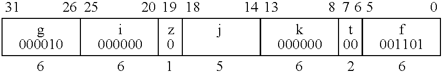 |
| TABLE 11 |
| |
Format: Ai,DL [Aj],AFADD,Ak,hint SCALAR
Purpose: Perform an atomic fetch-and-add on a memory location
Description:
| TABLE 12 |
| |
Format: Ai,DL [Aj],ACSWAP,Ak SCALAR
Purpose: Perform an atomic masked swap on a memory location
Description:
-
- StoreMemory(D, ValueAR(k, D), pAddr)
| TABLE 13 |
| |
Format: Ai,DL [Aj],AFAX,Ak SCALAR
Purpose: Perform an atomic fetch and a logic function on a memory location
Description:
| TABLE 14 |
| Truth Table for Masked Logical Instructions |
| Result Ai | ||||
| Ai | Ak | Prev Mem | New Memory | (from Prev Mem) |
| 0 | 0 | 0 | 0 (from Ak) | 0 |
| 0 | 0 | 1 | 0 (Ak) | 1 |
| 0 | 1 | 0 | 1 (Ak) | 0 |
| 0 | 1 | 1 | 1 (Ak) | 1 |
| 1 | 0 | 0 | 0 (Prev Mem) | 0 |
| 1 | 0 | 1 | 1 (Prev Mem) | 1 |
| 1 | 1 | 0 | 1 ( | 0 |
| Mem) | ||||
| 1 | 1 | 1 | 0 ( | 1 |
| Mem) | ||||
The following Table 15 shows how to set Ai and Ak to accomplish various logical functions to memory.
| TABLE 15 |
| Logical Operations for Masked Logical Instructions |
| Memory Result | |||
| Function | Ai | Ak | in (Aj) |
| AND (Force clear on 0- | operand | All zeros | (Aj) And operand |
| bits) | |||
| OR (Force set on 1-bits) | ~operand | operand | (Aj) Or operand |
| XOR | All ones | operand | (Aj) Xor operand |
| EQV | All ones | ~operand | (Aj) Eqv operand |
| Store under mask | mask | operand, except | Store operand |
| (0 in mask stores | 0s where mask | under mask | |
| operand) | is 1s | ||
| TABLE 16 |
| |
Format: [Aj] Ai,DL,AADD SCALAR
Purpose: Perform an atomic integer add to a memory location
Description:
| TABLE 17 |
| |
Format: [Aj]Ai,DL,AAX,Ak SCALAR
Purpose: Perform an atomic masked store on a memory location
Description:
Claims (11)
Priority Applications (5)
| Application Number | Priority Date | Filing Date | Title |
|---|---|---|---|
| US10/643,588 US7529906B2 (en) | 2003-08-18 | 2003-08-18 | Sharing memory within an application using scalable hardware resources |
| US10/643,741 US7437521B1 (en) | 2003-08-18 | 2003-08-18 | Multistream processing memory-and barrier-synchronization method and apparatus |
| EP04781494A EP1665054A2 (en) | 2003-08-18 | 2004-08-18 | Decoupled store address and data in a multiprocessor system |
| EP10010396A EP2284711A1 (en) | 2003-08-18 | 2004-08-18 | Decoupled store address and data in a multiprocessor system |
| PCT/US2004/026814 WO2005020088A2 (en) | 2003-08-18 | 2004-08-18 | Decoupled store address and data in a multiprocessor system |
Applications Claiming Priority (1)
| Application Number | Priority Date | Filing Date | Title |
|---|---|---|---|
| US10/643,741 US7437521B1 (en) | 2003-08-18 | 2003-08-18 | Multistream processing memory-and barrier-synchronization method and apparatus |
Publications (1)
| Publication Number | Publication Date |
|---|---|
| US7437521B1 true US7437521B1 (en) | 2008-10-14 |
Family
ID=39828423
Family Applications (1)
| Application Number | Title | Priority Date | Filing Date |
|---|---|---|---|
| US10/643,741 Active 2026-02-02 US7437521B1 (en) | 2003-08-18 | 2003-08-18 | Multistream processing memory-and barrier-synchronization method and apparatus |
Country Status (1)
| Country | Link |
|---|---|
| US (1) | US7437521B1 (en) |
Cited By (49)
| Publication number | Priority date | Publication date | Assignee | Title |
|---|---|---|---|---|
| US20050044340A1 (en) * | 2003-08-18 | 2005-02-24 | Kitrick Sheets | Remote translation mechanism for a multinode system |
| US20050044128A1 (en) * | 2003-08-18 | 2005-02-24 | Scott Steven L. | Decoupled store address and data in a multiprocessor system |
| US20070271569A1 (en) * | 2006-05-19 | 2007-11-22 | Sony Ericsson Mobile Communications Ab | Distributed audio processing |
| US20090178059A1 (en) * | 2008-01-07 | 2009-07-09 | Christian Alexander Lang | Method and system for providing consistency in processing data streams |
| US20100100682A1 (en) * | 2008-10-22 | 2010-04-22 | International Business Machines Corporation | Victim Cache Replacement |
| US20100100683A1 (en) * | 2008-10-22 | 2010-04-22 | International Business Machines Corporation | Victim Cache Prefetching |
| US20100153647A1 (en) * | 2008-12-16 | 2010-06-17 | International Business Machines Corporation | Cache-To-Cache Cast-In |
| US7793073B2 (en) | 2003-08-18 | 2010-09-07 | Cray Inc. | Method and apparatus for indirectly addressed vector load-add-store across multi-processors |
| US20100235584A1 (en) * | 2009-03-11 | 2010-09-16 | International Business Machines Corporation | Lateral Castout (LCO) Of Victim Cache Line In Data-Invalid State |
| US20100235577A1 (en) * | 2008-12-19 | 2010-09-16 | International Business Machines Corporation | Victim cache lateral castout targeting |
| US20100235576A1 (en) * | 2008-12-16 | 2010-09-16 | International Business Machines Corporation | Handling Castout Cache Lines In A Victim Cache |
| US20100257316A1 (en) * | 2009-04-07 | 2010-10-07 | International Business Machines Corporation | Virtual Barrier Synchronization Cache Castout Election |
| US20100257317A1 (en) * | 2009-04-07 | 2010-10-07 | International Business Machines Corporation | Virtual Barrier Synchronization Cache |
| US20100262784A1 (en) * | 2009-04-09 | 2010-10-14 | International Business Machines Corporation | Empirically Based Dynamic Control of Acceptance of Victim Cache Lateral Castouts |
| US20100262778A1 (en) * | 2009-04-09 | 2010-10-14 | International Business Machines Corporation | Empirically Based Dynamic Control of Transmission of Victim Cache Lateral Castouts |
| US20100262720A1 (en) * | 2009-04-09 | 2010-10-14 | International Buisness Machines Corporation | Techniques for write-after-write ordering in a coherency managed processor system that employs a command pipeline |
| US20100262783A1 (en) * | 2009-04-09 | 2010-10-14 | International Business Machines Corporation | Mode-Based Castout Destination Selection |
| US20110078249A1 (en) * | 2009-09-28 | 2011-03-31 | International Business Machines Corporation | Shared address collectives using counter mechanisms |
| US20110161589A1 (en) * | 2009-12-30 | 2011-06-30 | International Business Machines Corporation | Selective cache-to-cache lateral castouts |
| US20110219209A1 (en) * | 2010-03-04 | 2011-09-08 | Oracle International Corporation | Dynamic atomic bitsets |
| US20110264863A1 (en) * | 2007-12-31 | 2011-10-27 | Eric Sprangle | Device, system, and method for using a mask register to track progress of gathering elements from memory |
| WO2012015430A1 (en) * | 2010-07-30 | 2012-02-02 | Hewlett-Packard Development Company, L.P. | Computer system and method for sharing computer memory |
| WO2012015431A1 (en) * | 2010-07-30 | 2012-02-02 | Hewlett-Packard Development Company, L.P. | Computer system and method for sharing computer memory |
| US20120060016A1 (en) * | 2010-09-07 | 2012-03-08 | International Business Machines Corporation | Vector Loads from Scattered Memory Locations |
| US20120060015A1 (en) * | 2010-09-07 | 2012-03-08 | International Business Machines Corporation | Vector Loads with Multiple Vector Elements from a Same Cache Line in a Scattered Load Operation |
| US20120124332A1 (en) * | 2010-11-11 | 2012-05-17 | Fujitsu Limited | Vector processing circuit, command issuance control method, and processor system |
| US20120144089A1 (en) * | 2007-12-31 | 2012-06-07 | Hall Jonathan C | Scatter/gather accessing multiple cache lines in a single cache port |
| US8307194B1 (en) | 2003-08-18 | 2012-11-06 | Cray Inc. | Relaxed memory consistency model |
| US20140101353A1 (en) * | 2007-01-22 | 2014-04-10 | Renesas Electronics Corporation | Multi-processor device |
| CN103827815A (en) * | 2011-09-26 | 2014-05-28 | 英特尔公司 | Instruction and logic to provide vector loads and stores with strides and masking functionality |
| US20140195778A1 (en) * | 2011-09-26 | 2014-07-10 | Intel Corporation | Instruction and logic to provide vector load-op/store-op with stride functionality |
| CN104937576A (en) * | 2013-03-28 | 2015-09-23 | 惠普发展公司,有限责任合伙企业 | Coordinating replication of data stored in a non-volatile memory-based system |
| US9158685B2 (en) | 2012-09-11 | 2015-10-13 | Apple Inc. | System cache with cache hint control |
| WO2016154115A1 (en) * | 2015-03-20 | 2016-09-29 | Mill Computing, Inc. | Cpu security mechanisms employing thread-specific protection domains |
| US9563426B1 (en) * | 2013-12-30 | 2017-02-07 | EMC IP Holding Company LLC | Partitioned key-value store with atomic memory operations |
| KR20170093800A (en) * | 2014-12-12 | 2017-08-16 | 인텔 코포레이션 | Technologies for fast synchronization barriers for many-core processing |
| US9747218B2 (en) | 2015-03-20 | 2017-08-29 | Mill Computing, Inc. | CPU security mechanisms employing thread-specific protection domains |
| CN107111523A (en) * | 2014-11-11 | 2017-08-29 | 瑞萨电子株式会社 | Order executive control system and order perform control method |
| US9940128B2 (en) | 2015-10-06 | 2018-04-10 | International Business Machines Corporation | Conditional access with timeout |
| US10114651B2 (en) | 2009-12-22 | 2018-10-30 | Intel Corporation | Gathering and scattering multiple data elements |
| US20190199653A1 (en) * | 2017-12-27 | 2019-06-27 | International Business Machines Corporation | Reduced number of counters for reliable messaging |
| US10572400B2 (en) * | 2017-06-15 | 2020-02-25 | Mellanox Technologies, Ltd. | Shared processing of a packet flow by multiple cores |
| US10579585B2 (en) * | 2017-10-20 | 2020-03-03 | Graphcore Limited | Synchronization in a multi-tile, multi-chip processing arrangement |
| CN111240745A (en) * | 2019-02-20 | 2020-06-05 | 上海天数智芯半导体有限公司 | Enhanced scalar vector dual pipeline architecture for interleaved execution |
| CN111831337A (en) * | 2019-04-19 | 2020-10-27 | 安徽寒武纪信息科技有限公司 | Data synchronization method and device and related product |
| EP3796170A1 (en) * | 2019-09-20 | 2021-03-24 | Fujitsu Limited | Information processing apparatus, information processing system, and communication management program |
| US11204774B1 (en) * | 2020-08-31 | 2021-12-21 | Apple Inc. | Thread-group-scoped gate instruction |
| CN115129480A (en) * | 2022-08-26 | 2022-09-30 | 上海登临科技有限公司 | Scalar processing unit and access control method thereof |
| US11853758B2 (en) * | 2019-09-27 | 2023-12-26 | Intel Corporation | Techniques for decoupled access-execute near-memory processing |
Citations (98)
| Publication number | Priority date | Publication date | Assignee | Title |
|---|---|---|---|---|
| USRE28577E (en) | 1969-03-21 | 1975-10-21 | Channel reallocation system and method | |
| US4412303A (en) * | 1979-11-26 | 1983-10-25 | Burroughs Corporation | Array processor architecture |
| US4541046A (en) | 1981-03-25 | 1985-09-10 | Hitachi, Ltd. | Data processing system including scalar data processor and vector data processor |
| WO1987001750A1 (en) | 1985-09-16 | 1987-03-26 | Skandinova Byggsystem Aktiebolag | A building structure and a method for producing the same |
| US4771391A (en) | 1986-07-21 | 1988-09-13 | International Business Machines Corporation | Adaptive packet length traffic control in a local area network |
| WO1988008652A1 (en) | 1987-04-27 | 1988-11-03 | Thinking Machines Corporation | Method and apparatus for routing message packets |
| US4868818A (en) | 1987-10-29 | 1989-09-19 | The United States Of America As Represented By The Administrator Of The National Aeronautics And Space Administration | Fault tolerant hypercube computer system architecture |
| US4888679A (en) | 1988-01-11 | 1989-12-19 | Digital Equipment Corporation | Method and apparatus using a cache and main memory for both vector processing and scalar processing by prefetching cache blocks including vector data elements |
| EP0353819A2 (en) | 1988-08-02 | 1990-02-07 | Koninklijke Philips Electronics N.V. | Method and apparatus for synchronizing parallel processors using a fuzzy barrier |
| US4933933A (en) | 1986-12-19 | 1990-06-12 | The California Institute Of Technology | Torus routing chip |
| US4989131A (en) * | 1988-07-26 | 1991-01-29 | International Business Machines Corporation | Technique for parallel synchronization |
| US5008882A (en) | 1987-08-17 | 1991-04-16 | California Institute Of Technology | Method and apparatus for eliminating unsuccessful tries in a search tree |
| US5031211A (en) | 1989-02-03 | 1991-07-09 | Hitachi, Ltd. | Communication circuit switching or parallel operation system |
| US5036459A (en) | 1989-03-09 | 1991-07-30 | U.S. Philips Corporation | Multi-processor computer system with distributed memory and an interprocessor communication mechanism, and method for operating such mechanism |
| US5068851A (en) | 1989-08-01 | 1991-11-26 | Digital Equipment Corporation | Apparatus and method for documenting faults in computing modules |
| EP0473452A2 (en) | 1990-08-31 | 1992-03-04 | Ncr Corporation | Work station having multiprocessing capability |
| EP0475282A2 (en) | 1990-09-14 | 1992-03-18 | Hitachi, Ltd. | Synchronous method and apparatus for processors |
| US5105424A (en) | 1988-06-02 | 1992-04-14 | California Institute Of Technology | Inter-computer message routing system with each computer having separate routinng automata for each dimension of the network |
| EP0501524A2 (en) | 1983-05-31 | 1992-09-02 | W. Daniel Hillis | Parallel processor |
| US5157692A (en) | 1989-03-20 | 1992-10-20 | Fujitsu Limited | System for controlling communication between parallel computers |
| US5161156A (en) | 1990-02-02 | 1992-11-03 | International Business Machines Corporation | Multiprocessing packet switching connection system having provision for error correction and recovery |
| US5170482A (en) | 1987-08-14 | 1992-12-08 | Regents Of The University Of Minnesota | Improved hypercube topology for multiprocessor computer systems |
| US5175733A (en) | 1990-12-27 | 1992-12-29 | Intel Corporation | Adaptive message routing for multi-dimensional networks |
| US5197130A (en) | 1989-12-29 | 1993-03-23 | Supercomputer Systems Limited Partnership | Cluster architecture for a highly parallel scalar/vector multiprocessor system |
| US5218601A (en) | 1989-12-22 | 1993-06-08 | Fujitsu Limited | Method for searching for alternate path in communication network |
| US5218676A (en) | 1990-01-08 | 1993-06-08 | The University Of Rochester | Dynamic routing system for a multinode communications network |
| US5239545A (en) | 1990-11-05 | 1993-08-24 | Motorola, Inc. | Channel access control in a communication system |
| US5247691A (en) * | 1989-05-15 | 1993-09-21 | Fujitsu Limited | System for releasing suspended execution of scalar instructions following a wait instruction immediately upon change of vector post pending signal |
| US5247635A (en) * | 1989-03-28 | 1993-09-21 | Nec Corporation | Vector processing system for invalidating scalar cache memory block indicated by address in tentative vector store instruction |
| EP0570729A2 (en) | 1992-05-22 | 1993-11-24 | International Business Machines Corporation | Apap I/O programmable router |
| US5276899A (en) | 1981-04-01 | 1994-01-04 | Teredata Corporation | Multi processor sorting network for sorting while transmitting concurrently presented messages by message content to deliver a highest priority message |
| US5280474A (en) | 1990-01-05 | 1994-01-18 | Maspar Computer Corporation | Scalable processor to processor and processor-to-I/O interconnection network and method for parallel processing arrays |
| US5313645A (en) | 1991-05-13 | 1994-05-17 | International Business Machines Corporation | Method for interconnecting and system of interconnected processing elements by controlling network density |
| US5313628A (en) | 1991-12-30 | 1994-05-17 | International Business Machines Corporation | Component replacement control for fault-tolerant data processing system |
| US5331631A (en) | 1990-10-03 | 1994-07-19 | At&T Bell Laboratories | N+K sparing in a telecommunications switching environment |
| US5333279A (en) | 1992-06-01 | 1994-07-26 | Intel Corporation | Self-timed mesh routing chip with data broadcasting |
| US5341504A (en) | 1983-12-28 | 1994-08-23 | Hitachi, Ltd. | Multi-dimensional structured computer system |
| US5347450A (en) | 1989-01-18 | 1994-09-13 | Intel Corporation | Message routing in a multiprocessor computer system |
| US5353283A (en) | 1993-05-28 | 1994-10-04 | Bell Communications Research, Inc. | General internet method for routing packets in a communications network |
| US5365228A (en) | 1991-03-29 | 1994-11-15 | International Business Machines Corporation | SYNC-NET- a barrier synchronization apparatus for multi-stage networks |
| US5375223A (en) | 1993-01-07 | 1994-12-20 | International Business Machines Corporation | Single register arbiter circuit |
| US5418916A (en) | 1988-06-30 | 1995-05-23 | International Business Machines | Central processing unit checkpoint retry for store-in and store-through cache systems |
| WO1995016236A1 (en) | 1993-12-10 | 1995-06-15 | Cray Research, Inc. | Barrier synchronization for distributed memory massively parallel processing systems |
| US5430850A (en) | 1991-07-22 | 1995-07-04 | Massachusetts Institute Of Technology | Data processing system with synchronization coprocessor for multiple threads |
| US5440547A (en) | 1993-01-07 | 1995-08-08 | Kabushiki Kaisha Toshiba | Data-transfer routing management for packet-oriented digital communication system including ATM networks |
| US5446915A (en) | 1993-05-25 | 1995-08-29 | Intel Corporation | Parallel processing system virtual connection method and apparatus with protection and flow control |
| WO1996010283A1 (en) | 1994-09-27 | 1996-04-04 | Npr Technology Limited | Power cut-off device |
| US5517497A (en) | 1991-08-21 | 1996-05-14 | International Business Machines Corporation | Connectionless ATM data services |
| US5530933A (en) | 1994-02-24 | 1996-06-25 | Hewlett-Packard Company | Multiprocessor system for maintaining cache coherency by checking the coherency in the order of the transactions being issued on the bus |
| US5546549A (en) | 1994-06-01 | 1996-08-13 | International Business Machines Corporation | Multi-path channel (MPC) interface with user transparent, unbalanced, dynamically alterable computer input/output channels |
| US5548639A (en) | 1991-10-22 | 1996-08-20 | Fujitsu Limited | Distributed control of telecommunication network for setting up an alternative communication path |
| US5550589A (en) | 1991-09-03 | 1996-08-27 | Nec Corporation | Method of adaptively multiplexing a plurality of video channel data using channel data assignment information obtained from a look-up table |
| US5555542A (en) | 1991-06-19 | 1996-09-10 | Fujitsu Limited | Packet directional path identifier transfer system |
| WO1996032681A1 (en) | 1995-04-13 | 1996-10-17 | Cray Research, Inc. | Adaptive routing mechanism for torus interconnection network |
| US5649141A (en) | 1994-06-30 | 1997-07-15 | Nec Corporation | Multiprocessor system for locally managing address translation table |
| US5684977A (en) * | 1995-03-31 | 1997-11-04 | Sun Microsystems, Inc. | Writeback cancellation processing system for use in a packet switched cache coherent multiprocessor system |
| US5717895A (en) * | 1994-12-01 | 1998-02-10 | Cray Research, Inc. | Associative scalar data cache with write-through capabilities for a vector processor |
| US5721921A (en) | 1995-05-25 | 1998-02-24 | Cray Research, Inc. | Barrier and eureka synchronization architecture for multiprocessors |
| US5765009A (en) | 1994-02-22 | 1998-06-09 | Fujitsu Limited | Barrier synchronization system in parallel data processing |
| US5787494A (en) | 1992-10-06 | 1998-07-28 | Hewlett-Packard Company | Software assisted hardware TLB miss handler |
| US5796980A (en) | 1995-06-05 | 1998-08-18 | Advanced Micro Devices Inc. | Reducing cache snooping overhead in a multilevel cache system with inclusion field in shared cache indicating state of data in lower level caches |
| US5835951A (en) | 1994-10-18 | 1998-11-10 | National Semiconductor | Branch processing unit with target cache read prioritization protocol for handling multiple hits |
| US5860146A (en) | 1996-06-25 | 1999-01-12 | Sun Microsystems, Inc. | Auxiliary translation lookaside buffer for assisting in accessing data in remote address spaces |
| US5897664A (en) | 1996-07-01 | 1999-04-27 | Sun Microsystems, Inc. | Multiprocessor system having mapping table in each node to map global physical addresses to local physical addresses of page copies |
| US5987571A (en) | 1996-04-24 | 1999-11-16 | Hitachi, Ltd. | Cache coherency control method and multi-processor system using the same |
| US6003123A (en) | 1994-09-28 | 1999-12-14 | Massachusetts Institute Of Technology | Memory system with global address translation |
| US6014728A (en) | 1988-01-20 | 2000-01-11 | Advanced Micro Devices, Inc. | Organization of an integrated cache unit for flexible usage in supporting multiprocessor operations |
| US6088701A (en) | 1997-11-14 | 2000-07-11 | 3Dfx Interactive, Incorporated | Command data transport to a graphics processing device from a CPU performing write reordering operations |
| US6101590A (en) | 1995-10-10 | 2000-08-08 | Micro Unity Systems Engineering, Inc. | Virtual memory system with local and global virtual address translation |
| US6105113A (en) | 1997-08-21 | 2000-08-15 | Silicon Graphics, Inc. | System and method for maintaining translation look-aside buffer (TLB) consistency |
| US6161208A (en) | 1994-05-06 | 2000-12-12 | International Business Machines Corporation | Storage subsystem including an error correcting cache and means for performing memory to memory transfers |
| US6308316B1 (en) | 1993-11-30 | 2001-10-23 | Fujitsu Limited | Apparatus for analyzing operations of parallel processing system |
| US6317819B1 (en) * | 1996-01-11 | 2001-11-13 | Steven G. Morton | Digital signal processor containing scalar processor and a plurality of vector processors operating from a single instruction |
| US6339813B1 (en) | 2000-01-07 | 2002-01-15 | International Business Machines Corporation | Memory system for permitting simultaneous processor access to a cache line and sub-cache line sectors fill and writeback to a system memory |
| US6356983B1 (en) | 2000-07-25 | 2002-03-12 | Src Computers, Inc. | System and method providing cache coherency and atomic memory operations in a multiprocessor computer architecture |
| US6430649B1 (en) * | 1999-06-07 | 2002-08-06 | Sun Microsystems, Inc. | Method and apparatus for enforcing memory reference dependencies through a load store unit |
| US20020116600A1 (en) * | 1999-12-09 | 2002-08-22 | Smith Lawrence O. | Method and apparatus for processing events in a multithreaded processor |
| US20020169938A1 (en) | 2000-12-14 | 2002-11-14 | Scott Steven L. | Remote address translation in a multiprocessor system |
| US20020172199A1 (en) | 2000-12-14 | 2002-11-21 | Scott Steven L. | Node translation and protection in a clustered multiprocessor system |
| US6490671B1 (en) | 1999-05-28 | 2002-12-03 | Oracle Corporation | System for efficiently maintaining translation lockaside buffer consistency in a multi-threaded, multi-processor virtual memory system |
| US6496902B1 (en) | 1998-12-31 | 2002-12-17 | Cray Inc. | Vector and scalar data cache for a vector multiprocessor |
| US20030005380A1 (en) | 2001-06-29 | 2003-01-02 | Nguyen Hang T. | Method and apparatus for testing multi-core processors |
| US6519685B1 (en) | 1999-12-22 | 2003-02-11 | Intel Corporation | Cache states for multiprocessor cache coherency protocols |
| US20030097531A1 (en) | 2001-10-16 | 2003-05-22 | International Business Machines Corp. | Dynamic hardware and software performance optimizations for super-coherent SMP systems |
| US6591345B1 (en) | 2000-11-28 | 2003-07-08 | Hewlett-Packard Development Company, L.P. | Method for ensuring maximum bandwidth on accesses to strided vectors in a bank-interleaved cache |
| US20030167383A1 (en) | 2002-02-22 | 2003-09-04 | Ashish Gupta | System and method for memory interleaving using cell map with entry grouping for higher-way interleaving |
| US6684305B1 (en) | 2001-04-24 | 2004-01-27 | Advanced Micro Devices, Inc. | Multiprocessor system implementing virtual memory using a shared memory, and a page replacement method for maintaining paged memory coherence |
| US6782468B1 (en) | 1998-12-15 | 2004-08-24 | Nec Corporation | Shared memory type vector processing system, including a bus for transferring a vector processing instruction, and control method thereof |
| US6816960B2 (en) * | 2000-07-12 | 2004-11-09 | Nec Corporation | Cache consistent control of subsequent overlapping memory access during specified vector scatter instruction execution |
| US20050044339A1 (en) | 2003-08-18 | 2005-02-24 | Kitrick Sheets | Sharing memory within an application using scalable hardware resources |
| US20050044340A1 (en) | 2003-08-18 | 2005-02-24 | Kitrick Sheets | Remote translation mechanism for a multinode system |
| US20050044128A1 (en) | 2003-08-18 | 2005-02-24 | Scott Steven L. | Decoupled store address and data in a multiprocessor system |
| US6922766B2 (en) | 2002-09-04 | 2005-07-26 | Cray Inc. | Remote translation mechanism for a multi-node system |
| US6976155B2 (en) | 2001-06-12 | 2005-12-13 | Intel Corporation | Method and apparatus for communicating between processing entities in a multi-processor |
| US7028143B2 (en) | 2002-04-15 | 2006-04-11 | Broadcom Corporation | Narrow/wide cache |
| US20070283127A1 (en) | 2003-08-18 | 2007-12-06 | Cray Inc. | Method and apparatus for indirectly addressed vector load-add-store across multi-processors |
| US7334110B1 (en) | 2003-08-18 | 2008-02-19 | Cray Inc. | Decoupled scalar/vector computer architecture system and method |
| US7366873B1 (en) | 2003-08-18 | 2008-04-29 | Cray, Inc. | Indirectly addressed vector load-operate-store method and apparatus |
-
2003
- 2003-08-18 US US10/643,741 patent/US7437521B1/en active Active
Patent Citations (105)
| Publication number | Priority date | Publication date | Assignee | Title |
|---|---|---|---|---|
| USRE28577E (en) | 1969-03-21 | 1975-10-21 | Channel reallocation system and method | |
| US4412303A (en) * | 1979-11-26 | 1983-10-25 | Burroughs Corporation | Array processor architecture |
| US4541046A (en) | 1981-03-25 | 1985-09-10 | Hitachi, Ltd. | Data processing system including scalar data processor and vector data processor |
| US5276899A (en) | 1981-04-01 | 1994-01-04 | Teredata Corporation | Multi processor sorting network for sorting while transmitting concurrently presented messages by message content to deliver a highest priority message |
| EP0501524A2 (en) | 1983-05-31 | 1992-09-02 | W. Daniel Hillis | Parallel processor |
| US5341504A (en) | 1983-12-28 | 1994-08-23 | Hitachi, Ltd. | Multi-dimensional structured computer system |
| WO1987001750A1 (en) | 1985-09-16 | 1987-03-26 | Skandinova Byggsystem Aktiebolag | A building structure and a method for producing the same |
| US4771391A (en) | 1986-07-21 | 1988-09-13 | International Business Machines Corporation | Adaptive packet length traffic control in a local area network |
| US4933933A (en) | 1986-12-19 | 1990-06-12 | The California Institute Of Technology | Torus routing chip |
| WO1988008652A1 (en) | 1987-04-27 | 1988-11-03 | Thinking Machines Corporation | Method and apparatus for routing message packets |
| US5170482A (en) | 1987-08-14 | 1992-12-08 | Regents Of The University Of Minnesota | Improved hypercube topology for multiprocessor computer systems |
| US5008882A (en) | 1987-08-17 | 1991-04-16 | California Institute Of Technology | Method and apparatus for eliminating unsuccessful tries in a search tree |
| US4868818A (en) | 1987-10-29 | 1989-09-19 | The United States Of America As Represented By The Administrator Of The National Aeronautics And Space Administration | Fault tolerant hypercube computer system architecture |
| US4888679A (en) | 1988-01-11 | 1989-12-19 | Digital Equipment Corporation | Method and apparatus using a cache and main memory for both vector processing and scalar processing by prefetching cache blocks including vector data elements |
| US6014728A (en) | 1988-01-20 | 2000-01-11 | Advanced Micro Devices, Inc. | Organization of an integrated cache unit for flexible usage in supporting multiprocessor operations |
| US5105424A (en) | 1988-06-02 | 1992-04-14 | California Institute Of Technology | Inter-computer message routing system with each computer having separate routinng automata for each dimension of the network |
| US5418916A (en) | 1988-06-30 | 1995-05-23 | International Business Machines | Central processing unit checkpoint retry for store-in and store-through cache systems |
| US4989131A (en) * | 1988-07-26 | 1991-01-29 | International Business Machines Corporation | Technique for parallel synchronization |
| EP0353819A2 (en) | 1988-08-02 | 1990-02-07 | Koninklijke Philips Electronics N.V. | Method and apparatus for synchronizing parallel processors using a fuzzy barrier |
| US5347450A (en) | 1989-01-18 | 1994-09-13 | Intel Corporation | Message routing in a multiprocessor computer system |
| US5031211A (en) | 1989-02-03 | 1991-07-09 | Hitachi, Ltd. | Communication circuit switching or parallel operation system |
| US5036459A (en) | 1989-03-09 | 1991-07-30 | U.S. Philips Corporation | Multi-processor computer system with distributed memory and an interprocessor communication mechanism, and method for operating such mechanism |
| US5157692A (en) | 1989-03-20 | 1992-10-20 | Fujitsu Limited | System for controlling communication between parallel computers |
| US5247635A (en) * | 1989-03-28 | 1993-09-21 | Nec Corporation | Vector processing system for invalidating scalar cache memory block indicated by address in tentative vector store instruction |
| US5247691A (en) * | 1989-05-15 | 1993-09-21 | Fujitsu Limited | System for releasing suspended execution of scalar instructions following a wait instruction immediately upon change of vector post pending signal |
| US5068851A (en) | 1989-08-01 | 1991-11-26 | Digital Equipment Corporation | Apparatus and method for documenting faults in computing modules |
| US5218601A (en) | 1989-12-22 | 1993-06-08 | Fujitsu Limited | Method for searching for alternate path in communication network |
| US5640524A (en) | 1989-12-29 | 1997-06-17 | Cray Research, Inc. | Method and apparatus for chaining vector instructions |
| US5197130A (en) | 1989-12-29 | 1993-03-23 | Supercomputer Systems Limited Partnership | Cluster architecture for a highly parallel scalar/vector multiprocessor system |
| US5430884A (en) | 1989-12-29 | 1995-07-04 | Cray Research, Inc. | Scalar/vector processor |
| US5280474A (en) | 1990-01-05 | 1994-01-18 | Maspar Computer Corporation | Scalable processor to processor and processor-to-I/O interconnection network and method for parallel processing arrays |
| US5218676A (en) | 1990-01-08 | 1993-06-08 | The University Of Rochester | Dynamic routing system for a multinode communications network |
| US5161156A (en) | 1990-02-02 | 1992-11-03 | International Business Machines Corporation | Multiprocessing packet switching connection system having provision for error correction and recovery |
| EP0473452A2 (en) | 1990-08-31 | 1992-03-04 | Ncr Corporation | Work station having multiprocessing capability |
| EP0475282A2 (en) | 1990-09-14 | 1992-03-18 | Hitachi, Ltd. | Synchronous method and apparatus for processors |
| US5331631A (en) | 1990-10-03 | 1994-07-19 | At&T Bell Laboratories | N+K sparing in a telecommunications switching environment |
| US5239545A (en) | 1990-11-05 | 1993-08-24 | Motorola, Inc. | Channel access control in a communication system |
| US5175733A (en) | 1990-12-27 | 1992-12-29 | Intel Corporation | Adaptive message routing for multi-dimensional networks |
| US5365228A (en) | 1991-03-29 | 1994-11-15 | International Business Machines Corporation | SYNC-NET- a barrier synchronization apparatus for multi-stage networks |
| US5313645A (en) | 1991-05-13 | 1994-05-17 | International Business Machines Corporation | Method for interconnecting and system of interconnected processing elements by controlling network density |
| US5555542A (en) | 1991-06-19 | 1996-09-10 | Fujitsu Limited | Packet directional path identifier transfer system |
| US5560029A (en) | 1991-07-22 | 1996-09-24 | Massachusetts Institute Of Technology | Data processing system with synchronization coprocessor for multiple threads |
| US5430850A (en) | 1991-07-22 | 1995-07-04 | Massachusetts Institute Of Technology | Data processing system with synchronization coprocessor for multiple threads |
| US5517497A (en) | 1991-08-21 | 1996-05-14 | International Business Machines Corporation | Connectionless ATM data services |
| US5550589A (en) | 1991-09-03 | 1996-08-27 | Nec Corporation | Method of adaptively multiplexing a plurality of video channel data using channel data assignment information obtained from a look-up table |
| US5548639A (en) | 1991-10-22 | 1996-08-20 | Fujitsu Limited | Distributed control of telecommunication network for setting up an alternative communication path |
| US5313628A (en) | 1991-12-30 | 1994-05-17 | International Business Machines Corporation | Component replacement control for fault-tolerant data processing system |
| EP0570729A2 (en) | 1992-05-22 | 1993-11-24 | International Business Machines Corporation | Apap I/O programmable router |
| US5333279A (en) | 1992-06-01 | 1994-07-26 | Intel Corporation | Self-timed mesh routing chip with data broadcasting |
| US5787494A (en) | 1992-10-06 | 1998-07-28 | Hewlett-Packard Company | Software assisted hardware TLB miss handler |
| US5440547A (en) | 1993-01-07 | 1995-08-08 | Kabushiki Kaisha Toshiba | Data-transfer routing management for packet-oriented digital communication system including ATM networks |
| US5375223A (en) | 1993-01-07 | 1994-12-20 | International Business Machines Corporation | Single register arbiter circuit |
| US5446915A (en) | 1993-05-25 | 1995-08-29 | Intel Corporation | Parallel processing system virtual connection method and apparatus with protection and flow control |
| US5353283A (en) | 1993-05-28 | 1994-10-04 | Bell Communications Research, Inc. | General internet method for routing packets in a communications network |
| US6308316B1 (en) | 1993-11-30 | 2001-10-23 | Fujitsu Limited | Apparatus for analyzing operations of parallel processing system |
| US5434995A (en) | 1993-12-10 | 1995-07-18 | Cray Research, Inc. | Barrier synchronization for distributed memory massively parallel processing systems |
| WO1995016236A1 (en) | 1993-12-10 | 1995-06-15 | Cray Research, Inc. | Barrier synchronization for distributed memory massively parallel processing systems |
| US5765009A (en) | 1994-02-22 | 1998-06-09 | Fujitsu Limited | Barrier synchronization system in parallel data processing |
| US5530933A (en) | 1994-02-24 | 1996-06-25 | Hewlett-Packard Company | Multiprocessor system for maintaining cache coherency by checking the coherency in the order of the transactions being issued on the bus |
| US6161208A (en) | 1994-05-06 | 2000-12-12 | International Business Machines Corporation | Storage subsystem including an error correcting cache and means for performing memory to memory transfers |
| US5546549A (en) | 1994-06-01 | 1996-08-13 | International Business Machines Corporation | Multi-path channel (MPC) interface with user transparent, unbalanced, dynamically alterable computer input/output channels |
| US5649141A (en) | 1994-06-30 | 1997-07-15 | Nec Corporation | Multiprocessor system for locally managing address translation table |
| WO1996010283A1 (en) | 1994-09-27 | 1996-04-04 | Npr Technology Limited | Power cut-off device |
| US6003123A (en) | 1994-09-28 | 1999-12-14 | Massachusetts Institute Of Technology | Memory system with global address translation |
| US5835951A (en) | 1994-10-18 | 1998-11-10 | National Semiconductor | Branch processing unit with target cache read prioritization protocol for handling multiple hits |
| US5717895A (en) * | 1994-12-01 | 1998-02-10 | Cray Research, Inc. | Associative scalar data cache with write-through capabilities for a vector processor |
| US5684977A (en) * | 1995-03-31 | 1997-11-04 | Sun Microsystems, Inc. | Writeback cancellation processing system for use in a packet switched cache coherent multiprocessor system |
| WO1996032681A1 (en) | 1995-04-13 | 1996-10-17 | Cray Research, Inc. | Adaptive routing mechanism for torus interconnection network |
| US5721921A (en) | 1995-05-25 | 1998-02-24 | Cray Research, Inc. | Barrier and eureka synchronization architecture for multiprocessors |
| US5796980A (en) | 1995-06-05 | 1998-08-18 | Advanced Micro Devices Inc. | Reducing cache snooping overhead in a multilevel cache system with inclusion field in shared cache indicating state of data in lower level caches |
| US6101590A (en) | 1995-10-10 | 2000-08-08 | Micro Unity Systems Engineering, Inc. | Virtual memory system with local and global virtual address translation |
| US6317819B1 (en) * | 1996-01-11 | 2001-11-13 | Steven G. Morton | Digital signal processor containing scalar processor and a plurality of vector processors operating from a single instruction |
| US5987571A (en) | 1996-04-24 | 1999-11-16 | Hitachi, Ltd. | Cache coherency control method and multi-processor system using the same |
| US5860146A (en) | 1996-06-25 | 1999-01-12 | Sun Microsystems, Inc. | Auxiliary translation lookaside buffer for assisting in accessing data in remote address spaces |
| US5897664A (en) | 1996-07-01 | 1999-04-27 | Sun Microsystems, Inc. | Multiprocessor system having mapping table in each node to map global physical addresses to local physical addresses of page copies |
| US6105113A (en) | 1997-08-21 | 2000-08-15 | Silicon Graphics, Inc. | System and method for maintaining translation look-aside buffer (TLB) consistency |
| US6088701A (en) | 1997-11-14 | 2000-07-11 | 3Dfx Interactive, Incorporated | Command data transport to a graphics processing device from a CPU performing write reordering operations |
| US6782468B1 (en) | 1998-12-15 | 2004-08-24 | Nec Corporation | Shared memory type vector processing system, including a bus for transferring a vector processing instruction, and control method thereof |
| US6665774B2 (en) * | 1998-12-31 | 2003-12-16 | Cray, Inc. | Vector and scalar data cache for a vector multiprocessor |
| US6496902B1 (en) | 1998-12-31 | 2002-12-17 | Cray Inc. | Vector and scalar data cache for a vector multiprocessor |
| US6490671B1 (en) | 1999-05-28 | 2002-12-03 | Oracle Corporation | System for efficiently maintaining translation lockaside buffer consistency in a multi-threaded, multi-processor virtual memory system |
| US6430649B1 (en) * | 1999-06-07 | 2002-08-06 | Sun Microsystems, Inc. | Method and apparatus for enforcing memory reference dependencies through a load store unit |
| US6496925B1 (en) * | 1999-12-09 | 2002-12-17 | Intel Corporation | Method and apparatus for processing an event occurrence within a multithreaded processor |
| US20020116600A1 (en) * | 1999-12-09 | 2002-08-22 | Smith Lawrence O. | Method and apparatus for processing events in a multithreaded processor |
| US6519685B1 (en) | 1999-12-22 | 2003-02-11 | Intel Corporation | Cache states for multiprocessor cache coherency protocols |
| US6339813B1 (en) | 2000-01-07 | 2002-01-15 | International Business Machines Corporation | Memory system for permitting simultaneous processor access to a cache line and sub-cache line sectors fill and writeback to a system memory |
| US6816960B2 (en) * | 2000-07-12 | 2004-11-09 | Nec Corporation | Cache consistent control of subsequent overlapping memory access during specified vector scatter instruction execution |
| US6356983B1 (en) | 2000-07-25 | 2002-03-12 | Src Computers, Inc. | System and method providing cache coherency and atomic memory operations in a multiprocessor computer architecture |
| US6591345B1 (en) | 2000-11-28 | 2003-07-08 | Hewlett-Packard Development Company, L.P. | Method for ensuring maximum bandwidth on accesses to strided vectors in a bank-interleaved cache |
| US6925547B2 (en) | 2000-12-14 | 2005-08-02 | Silicon Graphics, Inc. | Remote address translation in a multiprocessor system |
| US20020169938A1 (en) | 2000-12-14 | 2002-11-14 | Scott Steven L. | Remote address translation in a multiprocessor system |
| US20020172199A1 (en) | 2000-12-14 | 2002-11-21 | Scott Steven L. | Node translation and protection in a clustered multiprocessor system |
| US6684305B1 (en) | 2001-04-24 | 2004-01-27 | Advanced Micro Devices, Inc. | Multiprocessor system implementing virtual memory using a shared memory, and a page replacement method for maintaining paged memory coherence |
| US6976155B2 (en) | 2001-06-12 | 2005-12-13 | Intel Corporation | Method and apparatus for communicating between processing entities in a multi-processor |
| US20030005380A1 (en) | 2001-06-29 | 2003-01-02 | Nguyen Hang T. | Method and apparatus for testing multi-core processors |
| US20030097531A1 (en) | 2001-10-16 | 2003-05-22 | International Business Machines Corp. | Dynamic hardware and software performance optimizations for super-coherent SMP systems |
| US20030167383A1 (en) | 2002-02-22 | 2003-09-04 | Ashish Gupta | System and method for memory interleaving using cell map with entry grouping for higher-way interleaving |
| US7028143B2 (en) | 2002-04-15 | 2006-04-11 | Broadcom Corporation | Narrow/wide cache |
| US6922766B2 (en) | 2002-09-04 | 2005-07-26 | Cray Inc. | Remote translation mechanism for a multi-node system |
| US20050044340A1 (en) | 2003-08-18 | 2005-02-24 | Kitrick Sheets | Remote translation mechanism for a multinode system |
| US20050044128A1 (en) | 2003-08-18 | 2005-02-24 | Scott Steven L. | Decoupled store address and data in a multiprocessor system |
| US20050044339A1 (en) | 2003-08-18 | 2005-02-24 | Kitrick Sheets | Sharing memory within an application using scalable hardware resources |
| US20070283127A1 (en) | 2003-08-18 | 2007-12-06 | Cray Inc. | Method and apparatus for indirectly addressed vector load-add-store across multi-processors |
| US7334110B1 (en) | 2003-08-18 | 2008-02-19 | Cray Inc. | Decoupled scalar/vector computer architecture system and method |
| US7366873B1 (en) | 2003-08-18 | 2008-04-29 | Cray, Inc. | Indirectly addressed vector load-operate-store method and apparatus |
Non-Patent Citations (99)
| Title |
|---|
| "Cray Assembly Language (CAL) for Cray X1(TM) Systems Reference Manual", Section 2.6, Memory Ordering, http://docs.cray.com/books/S-2314-51/index.html, (Jun. 2003), 302 pgs. |
| "Deadlock-Free Routing Schemes on Multistage Interconnection Networks", IBM Technical Disclosure Bulletin, 35, (Dec. 1992),232-233. |
| "ECPE 4504: Computer Organization Lecture 12: Computer Arithmetic", The Bradley Department of Electrical Engineering, (Oct. 17, 2000), 12 pgs. |
| "Msync-Synchronise Memory with Physical Storage", The Single UNIX Ä?Ä(R) Specification, Version 2: Msync, The Open Group, http://www.opengroup.org/nlinepubs/ 007908799/xsh/msync.html, (1997), 3 pgs. |
| Abts, D , "So Many States, So Little Time: Verifying Memory Coherence in the Cray X1", Parallel and Distributed Processing Symposium, (Apr. 22, 2003), 11-20. |
| Adve, V. S., et al., "Performance Analysis of Mesh Interconnection Networks with Deterministic Routing", Transactions on Parallel and Distributed Systems, (Mar. 1994),225-246. |
| Bolding, Kevin , "Non-Uniformities Introduced by Virtual Channel Deadlock Prevention", Technical Report 92-07-07, Department of Computer Science and Engineering, FR-35 University of Washington; Seattle, WA 98195 (Jul. 21, 1992). |
| Bolla, F R., "A Neural Strategy for Optimal Multiplexing of Circuit and Packet-Switched Traffic", Department of Communications, Computer and Systems Science (DIST), University of Genova, 1324-1330. |
| Boura, Y M., et al., "Efficient Fully Adaptive Wormhole Routing in n- dimenstional Meshes", IEEE, (1994),589-596. |
| Bundy, A. , et al., "Turning Eureka Stepsinto Calculations in Automatic Program", UK IT, (IEE Conf. Pub. 316), (1991),221-226. |
| Carlile, Bradley R., "Algorithms and Design: The Cray APP Shared-Memory System", COMPCON Spring '93. Digest of Papers., (Feb. 22, 1993), 312-320. |
| Chen, Y., et al., "UTLB: A Mechanism for Address Translation on Network Interfaces", Proceedings of the Eighth International Conference on Architectural Support for Programming Languages and Operating Systems (ASPLOS), (1998), 193-204. |
| Chien, A. A., et al., "Planar-Adaptive Routing: Low-Cost Adaptive Networks for Multiprocessors", Pro. 19th International. Symposium on Computer Architecture, (May 1992),268-277. |
| Cohoon, J., et al., C++ Program Design, 2nd Edition, McGraw-Hill Companies, Inc., (1999), p. 493. |
| Dally, W. J., "Virtual Channel Flow Control", Pro. 17th International Symposium on Computer Architecture, pp. 60-68, May 1990. |
| Dally, W. J., et al., "Deadlock-Free Adaptive Routing in Multicomputer Networks Using Virtual Channels", I.E.E.E. Transactions on Parallel and Distributed Systems, 4(4), (Apr. 1993),466-475. |
| Dally, William , "Performance Analysis of k-ary n-cube Interconnection Networks", IEEE Transactions on Computers, 39(6), (Jun. 1990),775-785. |
| Dally, William , et al., "Deadlock-Free Message Routing in Multiprocessor Interconnection Networks", IEEE Transactions on Computers, C-36, (May 1987),547-553. |
| Duato, J. , "A New Theory of Deadlock-Free Adaptive Routing in Wormhole Networks", I.E.E.E. Transactions on Parallel and Distributed Systems, 4(12), (Dec. 1993),1320-1331. |
| Ernst, D., et al., "Cyclone: A Broadcast-Free Dynamic Instruction Scheduler with Selective Replay", 30th Annual International Symposium on Computer Architecture (ISCA-2003), (Jun. 2003), 10 pgs. |
| Faanes, G. J., et al., "Decoupled Vector Architecture", U.S. Appl. No. 10/643,586, filed Aug. 18, 2003, 47 Pages. |
| Gallager, Robert , "Scale Factors for Distributed Routing Algorithm",NTC '77 Conference Record, 2, at 2-1 through 2-5. |
| Gharachorloo, Kourosh , "Two Techniques to Enhance the Performance of Memory Consistency Models", (1991). |
| Glass, C. J., et al., "The Turn Model for Adaptive Routing", Pro. 19th International Symposium on Computer architecture, (May 1992),278-287. |
| Gravano, L , et al., "Adaptive Deadlock- and Livelock-Free Routing with all Minimal Paths in Torus Networks", IEEE Transactions on Parallel and Distributed Systems, 5(12), (Dec. 1994),1233-1251. |
| Gupta, Rajiv , et al., "High speed Synchronization of Processors Using Fuzzy Barriers", International Journakl of Parallel Programming Feb. 19, 1990, No. 1, New York, US pp. 53-73. |
| Ishihata, Hiroaki , et al., "Architecture of Highly Parallel AP1000 Computer", Scripta Technica, Inc., Systems and Computers in Japan 24, No. 7,,(1993),pp. 69-76. |
| Jesshope, C. R., et al., "High Performance Communications in Processor Networks", Proc. 16th International Symposium on Computer Architecture, (May 1989),pp. 150-157. |
| Kirkpatrick, S. , et al., "Optimization by Simulated Annealing", Science, May 13, 1993, 220(4599), (May 1983),671-680. |
| Kontothanassis, L. , et al., "VM-Based Shared Memory on Low-Latency, Remote-Memory-Access Networks", Proceedings of the ACM ISCA '97, (1997), 157-169. |
| Linder, Daniel H., et al., "An Adaptive and Fault Tolerant Wormhole Routing Strategy for K-ary N-cubes", IEEE Transactions on Computers,40(1), (1991),pp. 2-12. |
| Lui, Z , et al., "Grouping Virtual Channels for Deadlock-Free Adaptive Wormhole Routing", PARLE '93 Parallel Parallel Architectures and Languages Europe, 5th International PARLE Conference, Munich, Germany\, (Jun. 14-17, 1993),254-265. |
| Nuth, Peter , et al., "The J-Machine Network", IEEE, (1992),pp. 420-423. |
| O'Keefe, Matthew T., et al., "Static Barrier MIMD: Architecture and Performance Analysis", Journal of Parallel and Distributed Computing No. 2., (Mar. 25, 1995),pp. 126-132. |
| Patterson, D. , et al., Computer Architecture: A Quantitative Approach, Second Edition, Morgan Kaufmann Publishers Inc. (1996), 251-256. |
| Patterson, D. A., et al., Computer Architecture A Quantitative Approach, 2nd Edition, Morgan Kaufmann Publishers, Inc., San Francisco,CA (1996), 255-260 & 308-317. |
| Patterson, D. A., et al., Computer Architecture: A Quantitative Approach, 2nd Edition, Morgan Kaufmann Publishers, Inc., San Francisco, CA, (1996), 194-197. |
| Patterson, D. A., et al., Computer Architecture: A Quantitative Approach, 2nd Edition, Morgan Kaufmann Publishers, Inc., San Francisco, CA, (1996), 699-708. |
| Patterson, D. A., et al., Computer Architecture: A Quantitative Approach, 2nd Edition, Morgan Kaufmann Publishers, San Francisco, CA (1996), 241-243. |
| Patterson, David A., et al., Computer Architecture: A Quantitative Approach, 2nd Edition, Morgan Kaufmann Publishers, Inc., San Francisco, CA,(1996), 179-187, 373-384. |
| Patterson, David A., et al., Computer Architecture: A Quantitative Approach, Second Edition, Morgan Kaufmann Publishers, Inc., San Francisco, CA,(1996), 39-41. |
| Scott, S. , "Synchronization and Communication in the T3E Multiprocessor", ASPLOS, vol. II, (1996),pp. 26-36. |
| Scott, S. L., "Decoupled Store Address and Data in a Multiprocessor System", U.S. Appl. No. 10/643,742, filed Aug. 18, 2003, 27 Pages. |
| Scott, S. L., "Latency Tolerant Distributed Shared Memory Multiprocessor Computer", U.S. Appl. No. 10/643,585, filed Aug. 18, 2003, 17 Pages. |
| Scott, S. L., et al., "Relaxed Memory Consistency Model", U.S. Appl. No. 10/643,754, filed Aug. 18, 2003, 144 Pages. |
| Sheets, K. , et al., "Remote-Translation Mechanism for a Multinode System", U.S. Appl. No. 10/643,758, filed Aug. 18, 2003, 42 Pages. |
| Shumay, M , "Deadlock-Free Packet Networks", Transputer Research and Applications 2, NATUG-2 Proceedings of the Second Conference of the North American Transputer Users Group, (Oct. 18-19, 1989),140-177. |
| Snyder, L. , "Introduction to the Configurable, Highly Parallel Computer", IEEE, (Jan. 1982),pp. 47-56. |
| Talia, D. , "Message-Routing Systems for Transputer-Based Multicomputer", IEEE Micro, vol. 13, No. 3, XP000380340, (Jun. 1993),62-72. |
| U.S. App. No. 10/643,586, Response filed Aug. 1, 2006 to Non-Final Office Action mailed Feb. 8, 2006, 24 pgs. |
| U.S. Appl. No. 10/235,898 Non Final Office Action mailed Jul. 7, 2004, 12 pgs. |
| U.S. Appl. No. 10/235,898 Notice of Allowance mailed Mar. 15, 2005, 4 pgs. |
| U.S. Appl. No. 10/235,898 Response filed Jan. 6, 2005 to Non Final Office Action mailed Jul. 7, 2004, 16 pgs. |
| U.S. Appl. No. 10/643,574, Advisory Action mailed May 21, 2007, 3 pgs. |
| U.S. Appl. No. 10/643,574, Final Office Action mailed Mar. 5, 2007, 31 pgs. |
| U.S. Appl. No. 10/643,574, Non-Final Office Action Mailed Aug. 7, 2007, 31 pgs. |
| U.S. Appl. No. 10/643,574, Non-Final Office Action mailed Jan. 30, 2006, 33 pgs. |
| U.S. Appl. No. 10/643,574, Non-Final Office Action mailed Jul. 28, 2006, 30 pgs. |
| U.S. Appl. No. 10/643,574, RCE and Response Under 37 C.F.R. 1.116 filed Jul. 12, 2007 to Final Office Action mailed Mar. 5, 2007, 19 pgs. |
| U.S. Appl. No. 10/643,574, Response filed May 1, 2006 to Non-Final Office mailed Jan. 30, 2006, 29 pgs. |
| U.S. Appl. No. 10/643,574, Response filed May 4, 2007 to Final Office Action mailed Mar. 5, 2007, 15 pgs. |
| U.S. Appl. No. 10/643,574, Response filed Nov. 28, 2006 to Non-Final Office mailed Jul. 28, 2006, 15 pgs. |
| U.S. Appl. No. 10/643,585, Advisory Action mailed Apr. 2, 2007, 3 pgs. |
| U.S. Appl. No. 10/643,585, Advisory Action mailed Aug. 14, 2006, 3 pgs. |
| U.S. Appl. No. 10/643,585, Amendment and Response filed Aug. 3, 2006 to Final Office Action mailed Apr. 14, 2006, 9 pgs. |
| U.S. Appl. No. 10/643,585, Amendment and Response filed Dec. 4, 2006 to Office Action mailed Oct. 23, 2006, 17 pgs. |
| U.S. Appl. No. 10/643,585, Amendment and Response filed Mar. 22, 2007 to Final Office Action mailed Jan. 25, 2007, 23 pgs. |
| U.S. Appl. No. 10/643,585, Amendment and Response filed Mar. 27, 2006 to Non-Final Office Action mailed Sep. 26, 2005, 7 pgs. |
| U.S. Appl. No. 10/643,585, Final Office Action mailed Apr. 14, 2006, 13 pgs. |
| U.S. Appl. No. 10/643,585, Final Office Action mailed Jan. 25, 2007, 17 pgs. |
| U.S. Appl. No. 10/643,585, Non-Final Office Action mailed Oct. 23, 2006, 12 pgs. |
| U.S. Appl. No. 10/643,585, Non-Final Office Action mailed Sep. 26, 2005, 9 pgs. |
| U.S. Appl. No. 10/643,585, Notice of Allowance mailed Jun. 11, 2007, 6 pgs. |
| U.S. Appl. No. 10/643,585, RCE and Amendment and Response filed Apr. 23, 2007 to Final Office Action mailed Jan. 25, 2007 and the Advisory Action mailed Apr. 2, 2007, 15 pgs. |
| U.S. Appl. No. 10/643,585, Response to Rule 312 Communication mailed Jul. 23, 2007, 2 pgs. |
| U.S. Appl. No. 10/643,586 Response to Non-Final Office Action filed Sep. 4, 2007, 18 pgs. |
| U.S. Appl. No. 10/643,586, Advisory Action mailed Jan. 18, 2007, 3 pgs. |
| U.S. Appl. No. 10/643,586, Final Office Action mailed Oct. 19, 2006, 27 pgs. |
| U.S. Appl. No. 10/643,586, Non-Final Office Action mailed Feb. 8, 2006, 21 pgs. |
| U.S. Appl. No. 10/643,586, Non-Final Office Action mailed May 2, 2007, 36 pgs. |
| U.S. Appl. No. 10/643,586, Notice of Allowance mailed Oct. 23, 2007, 5 pgs. |
| U.S. Appl. No. 10/643,586, RCE and Amendment and Response filed Feb. 16, 2007 to Final Office Action mailed Oct. 19, 2006 and the Advisory Action mailed Jan. 18, 2007, 19 pgs. |
| U.S. Appl. No. 10/643,586, Response filed Jan. 5, 2007 to Final Office Action mailed Oct. 19, 2006, 22 pgs. |
| U.S. Appl. No. 10/643,727, Non-Final Office Action mailed Aug. 11, 2006, 29 pgs. |
| U.S. Appl. No. 10/643,727, Non-Final Office Action mailed Feb. 16, 2006, 33 pgs. |
| U.S. Appl. No. 10/643,727, Notice of Allowance mailed Feb. 28, 2007, 5 pgs. |
| U.S. Appl. No. 10/643,727, Notice of Allowance mailed Jul. 19, 2007, 5 pgs. |
| U.S. Appl. No. 10/643,727, Response filed Jan. 11, 2007 to Non-Final Office Action mailed Aug. 11, 2006, 15 pgs. |
| U.S. Appl. No. 10/643,727, Response filed Jun. 15, 2006 to Non-Final Office Action mailed Feb. 16, 2006, 21 pgs. |
| U.S. Appl. No. 10/643,738 Response filed Jan. 16, 2006 non-final office action mailed Sep. 26, 2005, 13 pgs. |
| U.S. Appl. No. 10/643,738 Response filed Jul. 19, 2006 non-final office action mailed Feb. 17, 2006, 10 pgs. |
| U.S. Appl. No. 10/643,738, Final Office Action mailed Apr. 17, 2007, 12 pgs. |
| U.S. Appl. No. 10/643,738, Non-Final Office Action mailed Nov. 1, 2007, 19 pgs. |
| US 7,243,211, 07/2007, Kohn (withdrawn) |
| Wang, Weilin , et al., "Trunk Congestion Control in Heterogeneous Circuit Switched Networks", IEEE, (Jul. 1992),pp. 1156-1161. |
| Wood, D. A., et al., "An In-Cache Address Translation Mechanism", Proceedings of the 13th Annual International Symposium on Computer Architecture, (1986), 358-365. |
| Wu, Min-You , et al., "Do and Forall: Temporal and Spacial Control Structures", Proceedings, Third Workshop on Compilers for Parallel Computers, ACPC/TR, Jul. 1992. |
| Yang, C. S., et al., "Performance Evaluation of Multicast Wormhole Routing in 2D-Torus Multicomputers", IEEE, (1992),173-178. |
| Yantchev, J. , et al., "Adoptive, low latency, deadlock-free packet routing for networks of processors\", IEEE Proceedings, 136, (May 1989),pp. 178-186. |
Cited By (96)
| Publication number | Priority date | Publication date | Assignee | Title |
|---|---|---|---|---|
| US7743223B2 (en) | 2003-08-18 | 2010-06-22 | Cray Inc. | Decoupling of write address from its associated write data in a store to a shared memory in a multiprocessor system |
| US8307194B1 (en) | 2003-08-18 | 2012-11-06 | Cray Inc. | Relaxed memory consistency model |
| US20050044340A1 (en) * | 2003-08-18 | 2005-02-24 | Kitrick Sheets | Remote translation mechanism for a multinode system |
| US20050044128A1 (en) * | 2003-08-18 | 2005-02-24 | Scott Steven L. | Decoupled store address and data in a multiprocessor system |
| US7577816B2 (en) | 2003-08-18 | 2009-08-18 | Cray Inc. | Remote translation mechanism for a multinode system |
| US7793073B2 (en) | 2003-08-18 | 2010-09-07 | Cray Inc. | Method and apparatus for indirectly addressed vector load-add-store across multi-processors |
| US20070271569A1 (en) * | 2006-05-19 | 2007-11-22 | Sony Ericsson Mobile Communications Ab | Distributed audio processing |
| US7778822B2 (en) * | 2006-05-19 | 2010-08-17 | Sony Ericsson Mobile Communications Ab | Allocating audio processing among a plurality of processing units with a global synchronization pulse |
| US20140101353A1 (en) * | 2007-01-22 | 2014-04-10 | Renesas Electronics Corporation | Multi-processor device |
| US10372654B2 (en) | 2007-01-22 | 2019-08-06 | Renesas Electronics Corporation | Multi-processor device |
| US20110264863A1 (en) * | 2007-12-31 | 2011-10-27 | Eric Sprangle | Device, system, and method for using a mask register to track progress of gathering elements from memory |
| US20120144089A1 (en) * | 2007-12-31 | 2012-06-07 | Hall Jonathan C | Scatter/gather accessing multiple cache lines in a single cache port |
| US10387151B2 (en) * | 2007-12-31 | 2019-08-20 | Intel Corporation | Processor and method for tracking progress of gathering/scattering data element pairs in different cache memory banks |
| US10042814B2 (en) | 2007-12-31 | 2018-08-07 | Intel Corporation | System and method for using a mask register to track progress of gathering and scattering elements between data registers and memory |
| US8892848B2 (en) * | 2007-12-31 | 2014-11-18 | Intel Corporation | Processor and system using a mask register to track progress of gathering and prefetching elements from memory |
| US8291005B2 (en) * | 2008-01-07 | 2012-10-16 | International Business Machines Corporation | Providing consistency in processing data streams |
| US20090178059A1 (en) * | 2008-01-07 | 2009-07-09 | Christian Alexander Lang | Method and system for providing consistency in processing data streams |
| US20100100682A1 (en) * | 2008-10-22 | 2010-04-22 | International Business Machines Corporation | Victim Cache Replacement |
| US8347037B2 (en) | 2008-10-22 | 2013-01-01 | International Business Machines Corporation | Victim cache replacement |
| US8209489B2 (en) | 2008-10-22 | 2012-06-26 | International Business Machines Corporation | Victim cache prefetching |
| US20100100683A1 (en) * | 2008-10-22 | 2010-04-22 | International Business Machines Corporation | Victim Cache Prefetching |
| US20100153647A1 (en) * | 2008-12-16 | 2010-06-17 | International Business Machines Corporation | Cache-To-Cache Cast-In |
| US8499124B2 (en) | 2008-12-16 | 2013-07-30 | International Business Machines Corporation | Handling castout cache lines in a victim cache |
| US20100235576A1 (en) * | 2008-12-16 | 2010-09-16 | International Business Machines Corporation | Handling Castout Cache Lines In A Victim Cache |
| US8225045B2 (en) | 2008-12-16 | 2012-07-17 | International Business Machines Corporation | Lateral cache-to-cache cast-in |
| US8489819B2 (en) | 2008-12-19 | 2013-07-16 | International Business Machines Corporation | Victim cache lateral castout targeting |
| US20100235577A1 (en) * | 2008-12-19 | 2010-09-16 | International Business Machines Corporation | Victim cache lateral castout targeting |
| US8949540B2 (en) | 2009-03-11 | 2015-02-03 | International Business Machines Corporation | Lateral castout (LCO) of victim cache line in data-invalid state |
| US20100235584A1 (en) * | 2009-03-11 | 2010-09-16 | International Business Machines Corporation | Lateral Castout (LCO) Of Victim Cache Line In Data-Invalid State |
| US20100257317A1 (en) * | 2009-04-07 | 2010-10-07 | International Business Machines Corporation | Virtual Barrier Synchronization Cache |
| US20100257316A1 (en) * | 2009-04-07 | 2010-10-07 | International Business Machines Corporation | Virtual Barrier Synchronization Cache Castout Election |
| US8131935B2 (en) * | 2009-04-07 | 2012-03-06 | International Business Machines Corporation | Virtual barrier synchronization cache |
| US8095733B2 (en) * | 2009-04-07 | 2012-01-10 | International Business Machines Corporation | Virtual barrier synchronization cache castout election |
| US20100262783A1 (en) * | 2009-04-09 | 2010-10-14 | International Business Machines Corporation | Mode-Based Castout Destination Selection |
| US20100262784A1 (en) * | 2009-04-09 | 2010-10-14 | International Business Machines Corporation | Empirically Based Dynamic Control of Acceptance of Victim Cache Lateral Castouts |
| US8230117B2 (en) | 2009-04-09 | 2012-07-24 | International Business Machines Corporation | Techniques for write-after-write ordering in a coherency managed processor system that employs a command pipeline |
| US20100262778A1 (en) * | 2009-04-09 | 2010-10-14 | International Business Machines Corporation | Empirically Based Dynamic Control of Transmission of Victim Cache Lateral Castouts |
| US20100262720A1 (en) * | 2009-04-09 | 2010-10-14 | International Buisness Machines Corporation | Techniques for write-after-write ordering in a coherency managed processor system that employs a command pipeline |
| US8312220B2 (en) | 2009-04-09 | 2012-11-13 | International Business Machines Corporation | Mode-based castout destination selection |
| US8327073B2 (en) | 2009-04-09 | 2012-12-04 | International Business Machines Corporation | Empirically based dynamic control of acceptance of victim cache lateral castouts |
| US8347036B2 (en) | 2009-04-09 | 2013-01-01 | International Business Machines Corporation | Empirically based dynamic control of transmission of victim cache lateral castouts |
| US8655962B2 (en) * | 2009-09-28 | 2014-02-18 | International Business Machines Corporation | Shared address collectives using counter mechanisms |
| US20110078249A1 (en) * | 2009-09-28 | 2011-03-31 | International Business Machines Corporation | Shared address collectives using counter mechanisms |
| US10114651B2 (en) | 2009-12-22 | 2018-10-30 | Intel Corporation | Gathering and scattering multiple data elements |
| US10175990B2 (en) | 2009-12-22 | 2019-01-08 | Intel Corporation | Gathering and scattering multiple data elements |
| US20110161589A1 (en) * | 2009-12-30 | 2011-06-30 | International Business Machines Corporation | Selective cache-to-cache lateral castouts |
| US9189403B2 (en) | 2009-12-30 | 2015-11-17 | International Business Machines Corporation | Selective cache-to-cache lateral castouts |
| US20110219209A1 (en) * | 2010-03-04 | 2011-09-08 | Oracle International Corporation | Dynamic atomic bitsets |
| US8417733B2 (en) * | 2010-03-04 | 2013-04-09 | Oracle International Corporation | Dynamic atomic bitsets |
| US9710426B2 (en) | 2010-07-30 | 2017-07-18 | Hewlett Packard Enterprise Development Lp | Computer system and method for sharing computer memory |
| TWI459211B (en) * | 2010-07-30 | 2014-11-01 | Hewlett Packard Development Co | Computer system and method for sharing computer memory |
| TWI452473B (en) * | 2010-07-30 | 2014-09-11 | Hewlett Packard Development Co | Computer system and method for sharing computer memory |
| US10187247B2 (en) | 2010-07-30 | 2019-01-22 | Hewlett Packard Enterprise Development Lp | Computer system and method for sharing computer memory |
| WO2012015431A1 (en) * | 2010-07-30 | 2012-02-02 | Hewlett-Packard Development Company, L.P. | Computer system and method for sharing computer memory |
| WO2012015430A1 (en) * | 2010-07-30 | 2012-02-02 | Hewlett-Packard Development Company, L.P. | Computer system and method for sharing computer memory |
| US20120060016A1 (en) * | 2010-09-07 | 2012-03-08 | International Business Machines Corporation | Vector Loads from Scattered Memory Locations |
| US8904153B2 (en) * | 2010-09-07 | 2014-12-02 | International Business Machines Corporation | Vector loads with multiple vector elements from a same cache line in a scattered load operation |
| US20120060015A1 (en) * | 2010-09-07 | 2012-03-08 | International Business Machines Corporation | Vector Loads with Multiple Vector Elements from a Same Cache Line in a Scattered Load Operation |
| US8874879B2 (en) * | 2010-11-11 | 2014-10-28 | Fujitsu Limited | Vector processing circuit, command issuance control method, and processor system |
| US20120124332A1 (en) * | 2010-11-11 | 2012-05-17 | Fujitsu Limited | Vector processing circuit, command issuance control method, and processor system |
| US20140195775A1 (en) * | 2011-09-26 | 2014-07-10 | Intel Corporation | Instruction and logic to provide vector loads and stores with strides and masking functionality |
| CN103827815B (en) * | 2011-09-26 | 2017-11-28 | 英特尔公司 | Instruction and the logic across vectorial loading and storage with mask function are utilized for providing |
| CN106951214B (en) * | 2011-09-26 | 2019-07-19 | 英特尔公司 | For the processor of vector load/store operations, system, medium and method |
| CN106951214A (en) * | 2011-09-26 | 2017-07-14 | 英特尔公司 | For providing instruction and logic using vector loading operation/storage operation across function |
| CN103827815A (en) * | 2011-09-26 | 2014-05-28 | 英特尔公司 | Instruction and logic to provide vector loads and stores with strides and masking functionality |
| US20140195778A1 (en) * | 2011-09-26 | 2014-07-10 | Intel Corporation | Instruction and logic to provide vector load-op/store-op with stride functionality |
| GB2507018B (en) * | 2011-09-26 | 2020-04-22 | Intel Corp | Instruction and logic to provide vector loads and stores with strides and masking functionality |
| US9672036B2 (en) * | 2011-09-26 | 2017-06-06 | Intel Corporation | Instruction and logic to provide vector loads with strides and masking functionality |
| US9804844B2 (en) * | 2011-09-26 | 2017-10-31 | Intel Corporation | Instruction and logic to provide stride-based vector load-op functionality with mask duplication |
| US9158685B2 (en) | 2012-09-11 | 2015-10-13 | Apple Inc. | System cache with cache hint control |
| CN104937576B (en) * | 2013-03-28 | 2018-08-31 | 慧与发展有限责任合伙企业 | Coordinate the duplication for the data being stored in the system based on nonvolatile memory |
| US20150317079A1 (en) * | 2013-03-28 | 2015-11-05 | Hewlett-Packard Development Company, L.P. | Coordinating replication of data stored in a non-volatile memory-based system |
| CN104937576A (en) * | 2013-03-28 | 2015-09-23 | 惠普发展公司,有限责任合伙企业 | Coordinating replication of data stored in a non-volatile memory-based system |
| US9678673B2 (en) * | 2013-03-28 | 2017-06-13 | Hewlett Packard Enterprise Development Lp | Coordinating replication of data stored in a non-volatile memory-based system |
| US9563426B1 (en) * | 2013-12-30 | 2017-02-07 | EMC IP Holding Company LLC | Partitioned key-value store with atomic memory operations |
| US20170300329A1 (en) * | 2014-11-11 | 2017-10-19 | Renesas Electronics Corporation | Instruction execution control system and instruction execution control method |
| CN107111523A (en) * | 2014-11-11 | 2017-08-29 | 瑞萨电子株式会社 | Order executive control system and order perform control method |
| CN107111523B (en) * | 2014-11-11 | 2020-10-20 | 瑞萨电子株式会社 | Command execution control system and command execution control method |
| KR20170093800A (en) * | 2014-12-12 | 2017-08-16 | 인텔 코포레이션 | Technologies for fast synchronization barriers for many-core processing |
| US10678700B2 (en) | 2015-03-20 | 2020-06-09 | Mill Computing, Inc. | CPU security mechanisms employing thread-specific protection domains |
| US9747218B2 (en) | 2015-03-20 | 2017-08-29 | Mill Computing, Inc. | CPU security mechanisms employing thread-specific protection domains |
| WO2016154115A1 (en) * | 2015-03-20 | 2016-09-29 | Mill Computing, Inc. | Cpu security mechanisms employing thread-specific protection domains |
| US9940128B2 (en) | 2015-10-06 | 2018-04-10 | International Business Machines Corporation | Conditional access with timeout |
| US10572400B2 (en) * | 2017-06-15 | 2020-02-25 | Mellanox Technologies, Ltd. | Shared processing of a packet flow by multiple cores |
| US10579585B2 (en) * | 2017-10-20 | 2020-03-03 | Graphcore Limited | Synchronization in a multi-tile, multi-chip processing arrangement |
| US20190199653A1 (en) * | 2017-12-27 | 2019-06-27 | International Business Machines Corporation | Reduced number of counters for reliable messaging |
| US10812416B2 (en) * | 2017-12-27 | 2020-10-20 | International Business Machines Corporation | Reduced number of counters for reliable messaging |
| CN111240745A (en) * | 2019-02-20 | 2020-06-05 | 上海天数智芯半导体有限公司 | Enhanced scalar vector dual pipeline architecture for interleaved execution |
| US20200264879A1 (en) * | 2019-02-20 | 2020-08-20 | Nanjing Iluvatar CoreX Technology Co., Ltd. (DBA "Iluvatar CoreX Inc. Nanjing") | Enhanced scalar vector dual pipeline architecture with cross execution |
| CN111831337A (en) * | 2019-04-19 | 2020-10-27 | 安徽寒武纪信息科技有限公司 | Data synchronization method and device and related product |
| EP3796170A1 (en) * | 2019-09-20 | 2021-03-24 | Fujitsu Limited | Information processing apparatus, information processing system, and communication management program |
| US11544118B2 (en) | 2019-09-20 | 2023-01-03 | Fujitsu Limited | Information processing apparatus, information processing system, and non-transitory computer-readable storage medium for storing communication management program |
| US11853758B2 (en) * | 2019-09-27 | 2023-12-26 | Intel Corporation | Techniques for decoupled access-execute near-memory processing |
| US11204774B1 (en) * | 2020-08-31 | 2021-12-21 | Apple Inc. | Thread-group-scoped gate instruction |
| CN115129480A (en) * | 2022-08-26 | 2022-09-30 | 上海登临科技有限公司 | Scalar processing unit and access control method thereof |
| CN115129480B (en) * | 2022-08-26 | 2022-11-08 | 上海登临科技有限公司 | Scalar processing unit and access control method thereof |
Similar Documents
| Publication | Publication Date | Title |
|---|---|---|
| US7437521B1 (en) | Multistream processing memory-and barrier-synchronization method and apparatus | |
| US8307194B1 (en) | Relaxed memory consistency model | |
| US7334110B1 (en) | Decoupled scalar/vector computer architecture system and method | |
| US11275590B2 (en) | Device and processing architecture for resolving execution pipeline dependencies without requiring no operation instructions in the instruction memory | |
| US7681018B2 (en) | Method and apparatus for providing large register address space while maximizing cycletime performance for a multi-threaded register file set | |
| US6606704B1 (en) | Parallel multithreaded processor with plural microengines executing multiple threads each microengine having loadable microcode | |
| US6983350B1 (en) | SDRAM controller for parallel processor architecture | |
| US7191321B2 (en) | Microengine for parallel processor architecture | |
| US5632023A (en) | Superscalar microprocessor including flag operand renaming and forwarding apparatus | |
| US7305500B2 (en) | Sram controller for parallel processor architecture including a read queue and an order queue for handling requests | |
| US5721855A (en) | Method for pipeline processing of instructions by controlling access to a reorder buffer using a register file outside the reorder buffer | |
| US9830158B2 (en) | Speculative execution and rollback | |
| US7024537B2 (en) | Data speculation based on addressing patterns identifying dual-purpose register | |
| US7647475B2 (en) | System for synchronizing an in-order co-processor with an out-of-order processor using a co-processor interface store data queue | |
| US7089400B1 (en) | Data speculation based on stack-relative addressing patterns | |
| US20010052053A1 (en) | Stream processing unit for a multi-streaming processor | |
| US7743223B2 (en) | Decoupling of write address from its associated write data in a store to a shared memory in a multiprocessor system | |
| EP2284711A1 (en) | Decoupled store address and data in a multiprocessor system | |
| US7519771B1 (en) | System and method for processing memory instructions using a forced order queue | |
| US7321964B2 (en) | Store-to-load forwarding buffer using indexed lookup | |
| JPH10187464A (en) | Method and system for generating multiscalar program | |
| Kang et al. | On-chip multiprocessor design |
Legal Events
| Date | Code | Title | Description |
|---|---|---|---|
| AS | Assignment |
Owner name: CRAY INC., WASHINGTON Free format text: ASSIGNMENT OF ASSIGNORS INTEREST;ASSIGNORS:SCOTT, STEVEN L.;FAANES, GREGORY J.;STEPHENSON, BRICK;AND OTHERS;REEL/FRAME:014888/0656 Effective date: 20040105 |
|
| FEPP | Fee payment procedure |
Free format text: PAYOR NUMBER ASSIGNED (ORIGINAL EVENT CODE: ASPN); ENTITY STATUS OF PATENT OWNER: LARGE ENTITY |
|
| STCF | Information on status: patent grant |
Free format text: PATENTED CASE |
|
| CC | Certificate of correction | ||
| FPAY | Fee payment |
Year of fee payment: 4 |
|
| FEPP | Fee payment procedure |
Free format text: PAYOR NUMBER ASSIGNED (ORIGINAL EVENT CODE: ASPN); ENTITY STATUS OF PATENT OWNER: LARGE ENTITY Free format text: PAYER NUMBER DE-ASSIGNED (ORIGINAL EVENT CODE: RMPN); ENTITY STATUS OF PATENT OWNER: LARGE ENTITY |
|
| FPAY | Fee payment |
Year of fee payment: 8 |
|
| MAFP | Maintenance fee payment |
Free format text: PAYMENT OF MAINTENANCE FEE, 12TH YEAR, LARGE ENTITY (ORIGINAL EVENT CODE: M1553); ENTITY STATUS OF PATENT OWNER: LARGE ENTITY Year of fee payment: 12 |