US7439824B2 - Bulk acoustic wave filter and method for eliminating unwanted side passbands - Google Patents
Bulk acoustic wave filter and method for eliminating unwanted side passbands Download PDFInfo
- Publication number
- US7439824B2 US7439824B2 US11/069,715 US6971505A US7439824B2 US 7439824 B2 US7439824 B2 US 7439824B2 US 6971505 A US6971505 A US 6971505A US 7439824 B2 US7439824 B2 US 7439824B2
- Authority
- US
- United States
- Prior art keywords
- thin film
- resonator
- series
- layer
- detuning
- Prior art date
- Legal status (The legal status is an assumption and is not a legal conclusion. Google has not performed a legal analysis and makes no representation as to the accuracy of the status listed.)
- Active
Links
Images


Classifications
-
- H—ELECTRICITY
- H03—ELECTRONIC CIRCUITRY
- H03H—IMPEDANCE NETWORKS, e.g. RESONANT CIRCUITS; RESONATORS
- H03H9/00—Networks comprising electromechanical or electro-acoustic devices; Electromechanical resonators
- H03H9/46—Filters
- H03H9/54—Filters comprising resonators of piezo-electric or electrostrictive material
- H03H9/56—Monolithic crystal filters
- H03H9/564—Monolithic crystal filters implemented with thin-film techniques
-
- H—ELECTRICITY
- H03—ELECTRONIC CIRCUITRY
- H03H—IMPEDANCE NETWORKS, e.g. RESONANT CIRCUITS; RESONATORS
- H03H9/00—Networks comprising electromechanical or electro-acoustic devices; Electromechanical resonators
- H03H9/02—Details
- H03H9/02007—Details of bulk acoustic wave devices
- H03H9/02086—Means for compensation or elimination of undesirable effects
- H03H9/02118—Means for compensation or elimination of undesirable effects of lateral leakage between adjacent resonators
Definitions
- the present invention generally relates to a bulk acoustic wave filter such as lattice filters or ladder filters fabricated from solidly mounted thin film bulk acoustic wave resonators and a method for eliminating unwanted side passbands in the filter response.
- a bulk acoustic wave filter such as lattice filters or ladder filters fabricated from solidly mounted thin film bulk acoustic wave resonators and a method for eliminating unwanted side passbands in the filter response.
- a solidly mounted or acoustic mirror type thin film bulk acoustic wave resonator filter 10 of the state of the art includes a resonator section 11 based on a piezolayer 19 of piezoelectric material, such as ZnO or AlN, and includes an acoustic mirror 12 , all mounted on a substrate 14 made for example, from glass.
- the thin film bulk acoustic wave resonators 16 , 18 convert sound waves to electric signals, and vice versa, and can be used as a filter in electronic circuits because of its frequency dependent electrical impedance.
- the acoustic mirror 12 of the thin film bulk acoustic wave resonator filter 10 is formed from a combination of reflecting layers 24 to 30 of materials of differing acoustic impedance.
- An acoustic mirror 12 is built up on the substrate 14 by depositing its various layers 24 to 30 of different materials so as to form a stack of reflecting layers 24 to 30 of different materials on the substrate 14 .
- a bottom electrode 20 , 32 is deposited on the acoustic mirror 12
- the piezolayer 19 of piezoelectric material is then deposited on the bottom electrode 20 , 32 forming a so called piezolayer 19 .
- a top electrode 21 , 33 is deposited on the piezolayer 19 .
- top and bottom electrodes 21 , 20 ; 33 , 32 and the piezolayer 19 is called the resonator section 11 of the device.
- the acoustic mirror 12 serves to reflect acoustic waves created by the resonator section 11 in response to a voltage applied to the piezolayer 19 across the electrodes 20 , 21 ; 32 , 33 , thereby acoustically isolating the substrate 14 from the piezolayer 19 .
- What is fundamentally required from the reflecting layers 24 to 30 is to have a good reflection of acoustic energy created in the piezoelectric material, such that this energy does not leak out of the resonator, ultimately causing an undesired loss of energy.
- the mechanical resonance frequency of a thin film bulk acoustic wave resonator filter 10 is determined by the time it takes the acoustic wave to make a trip from the top surface to the bottom, undergo a reflection, and return to the top. The thinner the device, the faster the wave returns.
- the resonance, or sympathetic vibration occurs at the frequency where a wave being input into the device constructively adds to the wave introduced in the previous cycle, but which has now returned to its original location.
- the resonance frequency of the bulk acoustic wave resonator is set by the thickness and properties (i.e., speed, density) of the films deposited.
- Bulk acoustic wave resonators are used as components for bandpass filters in e.g. the RF-section of a mobile phone.
- a filter may be a so-called ladder filter but can also be of the lattice type.
- a ladder filter for example shown in FIG. 10 , includes at least one so-called L-section, an L-section including a series resonator 22 and a shunt resonator 23 and thus consisting of an even number of resonators.
- a filter consists of an odd number of resonators.
- a 21 ⁇ 2-stage filter could have either two series resonators 22 and three shunt resonators 23 , or three series resonators 22 and two shunt resonators 23 .
- the shunt and series bulk acoustic wave resonators 22 , 23 are manufactured so as to resonate at different frequencies (typically, but not necessarily with all the series bulk acoustic wave resonators 22 at one frequency, and all the shunt bulk acoustic wave resonators 23 at another). This is established by increasing the acoustic thickness of the shunt bulk acoustic wave resonators layer stack 23 as shown in FIG. 1 and corresponding description.
- the shunt bulk acoustic wave resonator's resonance frequency are reduced by adding a greater thickness ⁇ d e of material to its top electrode 33 ; for example by or depositing a shunt detuning layer 31 on top of the top electrode 33 .
- FIG. 2 illustrates this phenomenon and shows an impedance plot of two bulk acoustic wave resonators forming respectively a shunt and a series bulk acoustic wave resonator of a ladder filter.
- the strong peaks P 1S , P 2S at approximately 1800 MHz correspond to the fundamental resonance modes M 1R , M 2R of the two bulk acoustic wave resonators, 16 , 17 shown in FIG. 1
- the weak peaks P 1S , P 2S at approximately 2800 MHz correspond to the above mentioned acoustic overmodes M 1S , M 2S .
- the dashed line 34 corresponds to the series bulk acoustic wave resonator 22
- the solid line corresponds to the shunt bulk acoustic wave resonator 23 shown in FIG. 1 .
- the over-mode M S shown in FIG. 3 does not correspond to the second or third or higher harmonics of the first order passband resonance mode M R .
- the frequency of the acoustic overmode M S lies between the first order passband resonance mode M R and the second harmonic resonance mode not shown in FIG. 3 .
- the fundamental resonance modes M 1R of the shunt and M 2R of the series resonators create the filter passband according to the filter specification
- the acoustic resonances M 1S and M 2S give rise to a “side passband” in the filter response which is shown in FIG. 3 where the corresponding transmission of the bulk acoustic wave passband filter is plotted as a function of the frequency.
- this side passband is typically quite narrow-banded and not very pronounced, it may fall into a frequency region in which strict stopband restrictions apply to maintain a proper predetermined filter characteristic in the respective application as shown for example in FIG. 3 . Therefore, there is a need for a new bulk acoustic wave filter formed from a plurality of series bulk acoustic wave resonators and shunt bulk acoustic wave resonators, wherein each of said plurality of bulk acoustic wave resonators has a set of resonance frequencies.
- a bulk acoustic wave filter comprising a substrate, carrying a first set of piezoelectric resonator means having a thin film resonator structure comprising a piezolayer; and bottom electrodes and top electrodes; a second set of piezoelectric resonator means having a thin film resonator structure, similar to the first set of resonator means, wherein the fundamental resonance frequency is shifted to lower frequencies by applying at least one differential detuning layer at a position above the piezo median plane, determining the bandwidth ⁇ f of the bulk acoustic wave filter, positioned side by side with the first set of resonator means; and acoustic mirror layers positioned between the substrate and the piezoelectric resonator means comprising stacked layers of alternating low acoustic impedance and high acoustic impedance; wherein the thin film bulk acoustic wave resonator filter has an overmode-detuning component in which at least one
- the piezolayer can be a layer comprising crystalline CdS, PZT, AlN and/or ZnO.
- the piezolayer may have a thickness of about one quarter of a wavelength of an acoustic resonance frequency, and wherein the piezo median plane is located at a thickness of about one eighth of the wavelength.
- a stack of acoustic mirror layers may comprise 2 to 8 low acoustic impedance layers and 1 to 7 high acoustic impedance layers.
- the stack of acoustic mirror layers may comprise as low acoustic impedance material SiO 2 and as high acoustic impedance material one of the group Si 3 N 4 , AlN, Cr, W or Mo.
- the acoustic mirror layer may have a thickness dm of about one quarter of the wavelength of the acoustic resonance frequency.
- the overmode-detuning component may provide a mismatch of the thickness of the bottom electrodes beneath the piezo median plane.
- the overmode-detuning component may provide a mismatch in the thickness beneath the piezo median plane of at least one of the acoustic mirror layers in the regions of the shunt resonator branch and/or the series resonator branch having a thickness mismatch in a range of about one-three-hundredth part to one-fiftieth part of one quarter of the wavelength of the acoustic resonance frequency.
- the top electrodes and the bottom electrodes may comprise a sandwich structure of at least two layers for each electrode, having a first layer in close contact to the piezoelectric layer and a second layer in close contact to the first layer, wherein the first layer is made of high acoustic impedance material compared to the second layer and the second layer is made of high electrical conductivity material compared to the first layer.
- the first layer can be made of W, Mo, Ta or Au preferably of W and the second layer can be made of Al, Ag or Cu, preferably of Al.
- the mismatch between the thickness of the electrodes can be provided by a mismatch of the thickness of the second layer.
- the object can also be achieved by a method of producing a bulk acoustic wave filter comprising the steps of providing a substrate; depositing on the substrate stacked layers of alternating low acoustic impedance and high acoustic impedance; performing on top of the acoustic mirror layers a first and a second set of piezoelectric resonator means having bottom electrodes toward the acoustic mirror layers and top electrodes; detuning the bandwidth ⁇ f of the bulk acoustic wave filters by shifting a fundamental resonance frequency to lower frequencies by applying at least one differential detuning layer at a position above a piezo median plane; and adding an overmode-detuning component by implementing one additional differential layer at a position below the piezo median plane for at least one of the resonators in the first set of piezoelectric resonator means.
- the step of detuning can be performed by thinning the piezolayer by selectively etching piezoelectric material from one of the resonator components to reduce thin film resonator thickness and to determine the bandwidth of the bulk acoustic wave filter.
- the step of selective etching produces the desired shape of the filter's bandpass response.
- Each of the thin film resonator can be formed by interposing piezoelectric material between electrodes on a die, wherein the step of detuning includes removing piezoelectric material from regions to form thin film resonator components.
- the method can be used for detuning thin film resonator filters formed from a plurality of thin film resonator components that are manufactured using thin film techniques on a single substrate and coupled in a network, and may comprise the step of fabricating each of the plurality of thin film resonator components with a required set of differing resonance frequencies to provide a filtering function by increasing the resonance frequency sets of certain thin film resonator components from a global starting value, wherein the step of increasing effected by selectively etching piezoelectric material from the certain thin film resonator components to reduce thin film resonator component thickness, the removal of piezoelectric material up-shifting the resonance frequency sets of certain thin film resonator components having the reduced component thickness with respect to resonance frequency sets of other thin film resonator components in the filter.
- the plurality of thin film resonator components can be coupled in series and shunt branches of the filter to form the network.
- the method can be used for detuning a ladder filter formed from a plurality of connected thin film resonator T-cells, each T-Cell containing a plurality of thin film resonator components, coupled in series and shunt branches, each of the thin film resonator components having a set of resonance frequencies, comprising: shifting the set of resonance frequencies of thin film resonator components in the series branches of the T-Cells upward with respect to resonance frequencies in the shunt branch thin film resonator components by removing piezoelectric material from a surface of the series branch thin film resonator components.
- Each of the thin film resonator components can be formed by interposing piezoelectric material between electrodes on a die, wherein the step of detuning includes removing piezoelectric material from regions which will form series thin film resonator components and/or the die, excluding that piezoelectric material in regions which will form shunt thin film resonator components.
- the method may be used for detuning a thin film resonator filter formed from a plurality of thin film resonator components electrically connected in series and shunt branches, each of the plurality of thin film resonator components including a piezolayer of piezoelectric material interposed between two electrodes and each thin film resonator component having a set of resonance frequencies, comprising: shifting the set of resonance frequencies of thin film resonator components in the shunt branches of the filter down with respect to the series branch thin film resonator components by depositing additional piezoelectric material in a region which forms the shunt branch thin film resonator components.
- the invention provides a bulk acoustic wave filter comprising a substrate.
- This substrate carries acoustic mirror layers having typically but not necessarily a thickness of about one quarter of said wavelength at said acoustic resonance frequency.
- the acoustic mirror layers are stacked in an alternating manner of low acoustic impedance and high acoustic impedance layers.
- first and second piezoelectric resonator means are positioned side by side. These piezoelectric resonator means have a thin film resonator structure.
- a thin film resonator structure comprises a piezolayer and bottom electrodes positioned on said uppermost acoustic mirror layer. Top electrodes are positioned on top of said piezolayer.
- the electrodes of the first piezoelectric resonator means can be electrically connected to a series resonator branch and the electrodes of the second piezoelectric resonator means can be electrically connected to a shunt resonator branch.
- a frequency shifting or detuning of the shunt resonators is established by increasing the thickness of the layerstack of the shunt resonator above the piezo median line Lm. This can be done by increasing the piezo-thickness of the shunt resonator or by increasing the thickness of the top electrode or by depositing an additional dielectric layer on top of the shunts top electrode. Alternatively, a corresponding layer of the series resonator can be thinned by appropriate etching means.
- such a layer is referred to as a “differential layer for a certain resonator (respectively a certain subset of resonators)”, meaning that it can either be formed by depositing an additional layer only under or over this resonator (respectively subset of resonators) or by thinning a corresponding layer for all other resonators.
- the fundamental resonance frequency for at least one of the resonators in the second set of piezoelectric resonator means is shifted to lower frequencies by applying at least one differential detuning layer at a position above the piezo median plane Lm, determining the bandwidth ⁇ f of said bulk acoustic wave filter.
- the first and second set of piezoelectric resonators are positioned side by side.
- the acoustic mirror layers are positioned between said substrate and said piezoelectric resonator means comprising stacked layers of alternating low acoustic impedance and high acoustic impedance.
- the thin film bulk acoustic wave resonator filter of the present invention comprises an overmode-detuning component in which at least one additional differential layer is applied at a position below the piezo median plane Lm for at least one of the resonators in the first set of piezoelectric resonator means.
- the bulk acoustic wave filter has an overmode-detuning component in that a thinning is provided in the thickness of at least one of the layers of the shunt resonator below the piezo median plane Lm.
- a thinning is provided in the thickness of at least one of the layers of the shunt resonator below the piezo median plane Lm. This is most conveniently established by etching a small part of the uppermost low-impedance mirror layer of the shunt resonator or alternatively by depositing a thin additional layer on the uppermost low-impedance mirror layer of the series resonator.
- This is in strict contrast to the traditional detuning scheme (i.e. for the fundamental resonance mode) since in the method according to the present invention the frequency of the series resonator is lowered with respect to resonance frequency of the shunt resonators.
- the goal of the traditional detuning scheme is exactly the opposite.
- the proposed method is based on a different frequency sensitivity of the fundamental versus the overmode to a change in layer thickness above and below Lm.
- the fundamental mode is highly sensitive to changes in the layerstack above Lm, whereas the overmode is highly sensitive to changes below Lm. It is thus also possible to establish the overmode-detuning also in one of the other mirror layers, as well as in the bottom electrode.
- This bulk acoustic wave filter has the advantage, that the above mentioned overmodes particularly between the first and second order resonance frequencies are suppressed and no side-passband occurs in the stop band region of the required filter specification, particularly for specifications related to mobile phones or to other cellular, wireless or fiber-optic communications as well as in computer or computer related information exchange or information sharing systems.
- the present advantageous arrangement of a first and second piezoelectric resonator means alternately in a series and a shunt relationship forms a ladder configuration.
- the series resonator branch of the first piezoelectric resonator means carries signals from an input toward an output port, whereas the shunt resonator branch of the second piezoelectric resonator means provides an alternative path for the signals to ground.
- the transmission or blocking characteristics of both series and shunt elements affect the final signal reaching the output port from the input.
- the bulk acoustic wave filter of the present invention has the advantage of allowing a precise filtering, particularly in the context of the increasingly crowded radio frequencies spectrum. It meets the strict physical requirements of being extremely robust, being able to be mass produced and being small. Further, it maintains the strict rejection and transmission characteristics by its large stop band attenuation, efficiently cleaning up signals at the front-end of mobile phones by said overmode-detuning component comprising a mismatch of the thickness of the uppermost acoustic mirror layers.
- the piezolayer is a layer comprising polycrystalline CdS, AlN and/or ZnO. These crystalline piezoelectric materials of the piezolayer convert electrical energy to mechanical energy and vice versa such that at its mechanical resonance frequency, the electrical behaviour of the device of the present invention changes abruptly. Electrical signals of particular frequencies easily pass through the resonators of the present bulk acoustic wave filter while others will be stopped successfully and will not be transmitted as a result of the present invention.
- a further preferred embodiment of the present invention comprises a stack of acoustic mirror layers having 2 to 8 low acoustic impedance layers and 1 to 7 high acoustic impedance layers, preferably 3 to 5 low acoustic impedance layers and 2 to 4 high acoustic impedance layers. Each layer has a thickness of about a quarter of a wavelength at the acoustic resonance frequency. The higher the number of alternating acoustic mirror layers the sharper the edges of the passband of the bulk acoustic wave filter.
- the stack of acoustic mirror layers comprises preferably as low acoustic impedance material SiO 2 or Si 3 N 4 and as high acoustic impedance material one of the group, AlN, Cr, W or Mo.
- the top electrodes and the bottom electrodes comprise a sandwich structure of at least two layers for each electrode.
- a first layer of these layers is in close contact to the piezoelectric layer, while the second layer is in close contact to the first layer.
- Said first layer of material within each electrode is selected and used to increase the effective coupling coefficient between the piezoelectric layer of material in the resonator and the electric fields resulting from the voltages applied to the electrodes.
- the second layer of material within each electrode is selected and used to decrease the electrical losses within the electrodes. Therefore the first layer is made of high acoustic impedance material like W, Ta or Au, preferably W compared to the second layer.
- the second layer is made of a high electrical conductivity material like Al, Ag or Cu preferably Al compared to the first layer.
- a method of producing a bulk acoustic wave filter comprises the following steps:
- a substrate is provided on which stacked layers of alternating low acoustic impedance and high acoustic impedance are deposited.
- a first and a second set of piezoelectric resonator means having bottom electrodes toward the acoustic mirror layers and having top electrodes are manufactured.
- the bandwidth ⁇ f of said bulk acoustic wave filter is determined by shifting the fundamental resonance frequency of the shunt resonators to lower frequencies by applying at least one differential detuning layer at a position above a piezo median plane (Lm).
- an overmode-detuning component is added by implementing one additional differential layer at a position below said piezo median plane (Lm) for at least one of the resonators in said first set of piezoelectric resonator means.
- a traditional detuning step is applied to create a set of resonance frequencies by thin film resonator components in the series or shunt branches by thinning or thickening predefined areas of the piezoelectric resonator means. Therefore a thinning of a piezolayer from the series resonator branch thin film resonator components to up-shift their set of resonance frequencies with respect to resonance frequencies of said shunt resonator branch thin film resonator components is performed or a thickening of the thickness of top electrodes from the shunt resonator branch thin film resonator components is carried out.
- An overmode detuning step of said acoustic overmode resonance frequency is carried out, by performing a thinning in the thickness of at least one of the uppermost acoustic mirror layers in the regions of said shunt resonator branch by thinning this acoustic mirror layer in a range of about one-fiftieth part to one-three-hundredth part of one quarter of the wavelength at said acoustic resonance frequency to detune the acoustic overmode resonance frequency.
- This method has the advantage that overmodes, particularly between the first and second order resonance frequencies, are shifted in frequency in such a way that no side-passband occurs in the stop region for the required filter specification particularly of specifications related to mobile phones or to other cellular, wireless or fiber-optic communications as well as in computer or computer related information exchange or information sharing systems.
- This method has the additional advantage, that a short thinning step of the uppermost acoustic mirror layer is performed before the deposition of bottom electrodes takes place.
- This thinning is performed by etching just several Nanometres from the uppermost acoustic mirror layer in the region of the shunt resonator branch to suppress side-passband frequencies in the passband region.
- the thinning range is between one-three-hundredth part to one-fiftieth part of one quarter of a wavelength at the acoustic resonance frequency.
- Thinning can easily be performed by wet etching, plasma etching, sputter etching or reactive ion etching.
- the region of the series resonator branch can be protected by a resist layer during the thinning process of the series resonator branch region.
- the step of detuning by enlarging the thickness of top electrodes of the shunt resonator branch has the advantage of being a cost effective method, since this step can be performed as a very last deposition step.
- this step can be performed as a very last deposition step.
- the step of detuning by thinning the piezolayer includes selectively etching piezoelectric material from the series branch thin film resonator components to reduce thin film resonator component thickness, wherein said step of selective etching produces the desired shape of the filter's passband response and determines the bandwidth of said bulk acoustic wave filter.
- Such a thinning to define the bandwidth of said bulk acoustic wave filter can be performed as soon as the piezolayer is deposited on the bottom electrodes. This thinning is selectively performed in the region of the series resonator branch.
- a thickness difference in the range of one-tenth part to one-twentieth part of the thickness of said piezolayer is etched, which is at least an order of magnitude more than the thinning for the overmode-detuning process. Therefore the detuning requirements to determine the passband width of the bulk acoustic wave filter performed within the piezolayer are not comparable with the overmode-detuning requirements performed within the acoustic mirror layer.
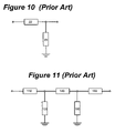
- said plurality of thin film resonator components are electrically connected coupled in series and shunt branches of the filter to form a network as for example shown in FIG. 11 .
- This network comprises T-cells, wherein each T-Cell contains a plurality of thin film resonator components coupled in series ( 110 , 140 , 160 ) and shunt branches ( 130 , 150 ).
- Each of said thin film resonator components have a set of resonance frequencies.
- An alternative method for detuning a thin film resonator filter is to shift the set of resonance frequencies of the thin film resonator components in the shunt branches of the filter down with respect to the series branch thin film resonator components by depositing additional piezoelectric material in a region which forms the shunt branch thin film resonator components.
- This method is somewhat different to the detuning methods already discussed, since it is necessary to enlarge the thickness of the piezolayer in the region of the shunt resonator branch of about one-half to one-twentieth of one half of a wavelength of an acoustic frequency resonance.
- This can be performed by depositing piezoelectric material by chemical vapour deposition or physical vapour deposition. This has to be done prior to the deposition of the shunt electrodes.
- FIG. 1 shows a schematic of an acoustic mirror type bulk acoustic wave resonator filter according to the prior art
- FIG. 2 shows an impedance plot of a series and a shunt bulk acoustic wave resonator forming said bulk acoustic wave passband filter of FIG. 1 ;
- FIG. 3 shows the transmission characteristics for the bulk acoustic wave passband filter of FIG. 1 ;
- FIG. 4 shows a schematic of an acoustic mirror type bulk acoustic wave resonator filter according to a first embodiment of the present invention
- FIG. 5 shows the displacement generated by a bulk acoustic wave within a series resonator in relation to the distance from a substrate at the first resonance frequency of 1870 MHz;
- FIG. 6 shows the displacement generated by a bulk acoustic wave within a series resonator in relation to the distance from a substrate at a frequency of an over-mode of 2800 MHz;
- FIG. 7 shows the influence of a mismatch in the range of 2 to 14 nm of the uppermost acoustic mirror layer between the region of the shunt resonator branch and the region of the series resonator branch;
- FIG. 8 shows the transmission characteristics for the bulk acoustic wave passband filter of FIG. 4 ;
- FIG. 9 shows a schematic of an acoustic mirror type bulk acoustic wave resonator filter according to a second embodiment of the present invention.
- FIG. 10 shows a typical branch of a ladder filter.
- FIG. 11 shows an exemplary network with T-Cells.
- FIG. 1 shows a schematic of an acoustic mirror type thin film bulk acoustic wave resonator filter 10 according to the prior art described above and FIG. 2 shows an impedance plot of a series and a shunt bulk acoustic wave resonator 22 , 23 forming said thin film bulk acoustic wave resonator filter 10 of FIG. 1 . Furthermore FIG. 3 shows the transmission characteristics for said thin film bulk acoustic wave resonator filter of FIG. 1 . As can be seen from FIG. 2 and FIG.
- the acoustic mirror type thin film bulk acoustic wave resonator filter 10 shows an over-mode resonance forming a weak side-passband filter between the first order resonance frequency of the filter and the second harmonic resonance frequency. This side-passband of the filter potentially violates the stop band specifications required for various filter applications.
- a new bulk acoustic wave resonator filter formed from a plurality of series bulk acoustic wave resonators and shunt bulk acoustic wave resonators.
- FIG. 4 shows a schematic of an acoustic mirror type thin film bulk acoustic wave resonator filter 40 according to a first embodiment of the present invention.
- This thin film bulk acoustic wave resonator filter 40 comprises a substrate 14 on which a stack of acoustic mirror layers 24 to 30 is deposited to form an acoustic mirror 12 .
- Each set acoustic mirror layer 24 to 30 has a thickness dm of about one quarter ⁇ /4 of a wavelength ⁇ at the acoustic resonance frequency.
- This stack of acoustic mirror layers 24 to 30 consists of four low acoustic impedance layers 24 , 26 , 28 and 30 and there between three acoustic mirror layers 25 , 27 and 29 of high acoustic impedance.
- the uppermost acoustic mirror layer 30 of low acoustic impedance comprises an overmode-detuning component 41 providing a mismatch between an area occupied by a first piezoelectric resonator means 16 and second piezoelectric resonator means 18 .
- This overmode-detuning component 41 provides a mismatch ⁇ d m in the thickness dm of the uppermost acoustic mirror layer 30 .
- This thickness mismatch ⁇ d m is in a range of about one-hundredth part to one-twohundredth part of one quarter ⁇ /4 of said acoustic wavelength ⁇ .
- This overmode-detuning component 41 of a thickness difference between the first piezoelectric resonator means 16 and the second piezoelectric resonator means 18 has the effect, that the above-mentioned side-passband filter characteristic is suppressed.
- Bottom electrodes 20 and 32 for a series resonator branch 22 and a shunt resonator branch 23 respectively are positioned on this uppermost acoustic mirror layer 30 .
- a piezolayer 19 is deposited with a thickness of about one quarter ⁇ /4 of the resonance wavelength ⁇ and on top of this piezolayer 19 the known top electrodes 21 and 33 of the series resonator branch 22 and the shunt resonator branch 23 respectively are positioned.
- the top electrode 33 is covered by a detuning component 31 having a thickness ⁇ d e of one-half down to one twentieth part of the thickness of said top electrode 33 .
- the resonator section 11 of the device of the present invention is identical with the resonator section 11 of the prior art shown in FIG. 1 .
- FIG. 5 shows the displacement generated by a bulk acoustic wave within a series resonator as a function of the distance from a substrate 14 at the first resonator frequency of 1870 MHz.
- the reason for the side pass-band shown in FIG. 3 is that the over-mode resonances of series and shunt resonators 22 and 23 of FIG. 1 show an appropriate frequency-separation that gives rise to the formation of a side-passband.
- the actual shape of the side-passband is a strong function of this separation, with a minimum insertion loss (or correspondingly a maximum violation of the passband specification) at a separation, where the shunt resonators parallel resonance and the serious resonator serious resonance have approximately the same frequency.
- the idea of the present invention is to provide a way to change this frequency separation of the over-modes in such a way, that the resulting side-passband feature does not violate the specification of the particular application, while at the same time the performance of the main passband is undistorted.
- FIG. 6 compared to FIG. 5 shows the displacement generated by a bulk acoustic wave within a series resonator as a function of the distance from a substrate 14 at a frequency of an over-mode of 2800 MHz.
- This comparison clearly reveals that the over-mode comes from an acoustic resonance in the mirror layers themselves rather than from a real over-mode of the fundamental resonance frequency of the piezolayer 19 .
- the real over-mode of the fundamental resonance frequency of the piezolayer 19 is expected at much higher frequencies like the second harmonic resonance at about 3.6 GHz or the third harmonic resonance at about 5.4 GHz.
- the unwanted first over-mode resonance at 2.8 GHz is predominately caused by a breathing of the upper two low acoustic impedance mirror layers around the field node at approximately 3 ⁇ m from the substrate surface at zero ⁇ m.
- the resonance frequency of the unwanted over-mode is a sensitive function of the layer thickness of the various acoustic mirror layers in particular of the uppermost low acoustic impedance mirror layer 30 and the low acoustic impedance mirror layer 28 .
- the over-mode resonance frequency shows very little sensitivity to variations in the thickness of layers of the resonator section 11 , particularly layers above the piezo median plan.
- the small resonator bandwidth (or low-coupling) nature of the over-modes only a rather small overmode-detuning is actually needed in order to give rise to a significant side-passband.
- layerstacks and detuning schemes for which the state-of-the-art detuning produces an adapted detuning for both the fundamental modes and the overmodes.
- the series resonators and the shunt resonators are detuned to build the required passband by adding an additional detuning component at the top or within the resonator section 11 .
- This detuning component is performed by creating a large thickness difference at the top or within the resonator section 11 and causes the large frequency shift of the first resonance frequency or the fundamental mode necessary to form a precise passband resonance mode M R with a band width ⁇ f, shown in FIG. 3 , while it leads at the same time to a small shift of the first over-mode that—if not compensated by the method according to the present invention—gives rise to an unwanted overmode side-passband filter M S , shown in FIG. 3 .
- the unwanted side-passband is caused predominately by the low acoustic impedance mirror layer 30 and not by the piezolayer 19 or by the top electrode, it is the idea of the present invention to slightly change the layer thickness of one of the acoustic mirror layers that show a sensitive effect on the over-mode frequency either for the series or for the shunt resonator branch in the thin bulk acoustic wave resonator film.
- said overmode-detuning component 41 shown in FIG. 4 the over-mode resonance peak P 1S shown in FIG. 2 of the acoustic over-mode M 1S of a first order resonance mode M 1R of the series resonator branch as shown in FIG.
- the over-mode resonance peak P 2S of an acoustic over-mode M 2S of a first order resonance mode M 2R of shunt resonance branch can be moved away from the unfortunate and unwanted case described above.
- the side-passband can be at least sufficiently suppressed.
- the effect of the overmode-detuning component 41 of FIG. 4 on the suppression of an over-mode M S of a side-passband filter is shown in the next figure.
- FIG. 7 shows the insertion loss of the side-passband in dB as a function of the frequency in GHz.
- the insertion loss for the stop band has to be in this case minus 15 dB.
- FIG. 7 shows now the influence of a thickness mismatch (overmode-detuning component 41 ) in the range of 2 to 14 nm of the uppermost acoustic mirror layer between the region of the shunt resonator branch and the region of the series resonator branch.
- a mismatch of only 4 nm is already sufficient to decrease the side-passband close to the stop band specification.
- a mismatch of 6 nm of the overmode-detuning component 41 shown in FIG. 4 has already the effect, that the stop band is nevermore violated.
- the fundamental difference between the traditional detuning scheme and the overmode-suppressing detuning scheme according to the present invention is that traditional seeks to increase the effective thickness of the shunt layer stack (and thereby lowering its resonance frequency) by either depositing at least one additional layer of material in the region of the shunt resonators or by making at least one of the common layers thicker with respect to the same layer in the series resonators.
- the scheme proposed by the present invention includes an additional differential layer with the completely reversed thickness strategy (i.e. being thicker for the series resonators) in order to reduce the frequency detuning of the overmodes and ultimately to eliminate the unwanted side-passband in the filter response.
- This mismatch can be achieved processing-wise by using a lithographic mask, that opens over those regions that are supposed to have a smaller layer thickness.
- a lithographic mask that opens over those regions that are supposed to have a smaller layer thickness.
- an appropriate portion of the exposed layer is etched by standard semiconductor processing methods like dry or wet etching or ion beam milling.
- the resist mask is removed and the production process for a thin film bulk acoustic wave resonator filter is continued in the usual way.
- the resist mask it is possible to use the resist mask as a lift-off mask in order to deposit an additional thin layer of material on top of the exposed surface region.
- the mask needs to open the opposite resonator type.
- the uppermost acoustic mirror layer 30 of the shunt resonators can be thinned so much that an inversion of the overmode-detuning takes place.
- Such an inversion results in the fact, that the shunt over-mode frequency is higher than the series over-mode frequency. This case is preferable since it completely eliminates the side-passband filter effect. (cf. FIG. 7 at 14 nm thickness mismatch).
- FIG. 8 shows the transmission characteristics for the bulk acoustic wave filter of FIG. 4 .
- the insertion loss in dB is shown as a function of the frequency in GHz.
- the stop band is characterised by a horizontal line close to an insertion loss of minus 15 dB.
- the side-passband is suppressed sufficiently by thinning the uppermost acoustic mirror layer 30 shown in FIG. 4 by about 10 nm to create a mismatch in the thickness of the uppermost acoustic mirror layer 30 between the region of the shunt resonator branch and the region of the series resonator branch.
- FIG. 9 shows a schematic of an acoustic mirror type thin film bulk acoustic wave resonator filter 50 according to a second embodiment of the present invention.
- the thickness of all electrodes 20 , 21 , 32 and 33 remain unchanged having no detuning component on top.
- the detuning component 31 of this second embodiment of the present invention is provided by a thickness difference ⁇ d p of the thickness dp of the piezolayer 19 in the range of one-tenth to one-twentieth in the region of the series resonator branch 22 .
- the overmode-detuning for suppressing the side-passband by a overmode-detuning component 41 is achieved similarly to the first embodiment according to FIG. 4 of the present invention.
Abstract
Description
Claims (25)
Applications Claiming Priority (2)
| Application Number | Priority Date | Filing Date | Title |
|---|---|---|---|
| EPEP04005574.1 | 2004-03-09 | ||
| EP04005574A EP1575165B1 (en) | 2004-03-09 | 2004-03-09 | Bulk acoustic wave filter and method for eliminating unwanted side passands |
Publications (2)
| Publication Number | Publication Date |
|---|---|
| US20050200433A1 US20050200433A1 (en) | 2005-09-15 |
| US7439824B2 true US7439824B2 (en) | 2008-10-21 |
Family
ID=34814277
Family Applications (1)
| Application Number | Title | Priority Date | Filing Date |
|---|---|---|---|
| US11/069,715 Active US7439824B2 (en) | 2004-03-09 | 2005-03-01 | Bulk acoustic wave filter and method for eliminating unwanted side passbands |
Country Status (5)
| Country | Link |
|---|---|
| US (1) | US7439824B2 (en) |
| EP (1) | EP1575165B1 (en) |
| JP (1) | JP4318653B2 (en) |
| CN (1) | CN100586010C (en) |
| DE (1) | DE602004013534D1 (en) |
Cited By (41)
| Publication number | Priority date | Publication date | Assignee | Title |
|---|---|---|---|---|
| US20070063622A1 (en) * | 2005-09-09 | 2007-03-22 | Rudy Richard C | Adjusted frequency temperature coefficient resonator |
| US20090146531A1 (en) * | 2003-03-07 | 2009-06-11 | Ruby Richard C | Manufacturing Process For Thin Film Bulk Acoustic Resonator (FBAR) Filters |
| US20100001813A1 (en) * | 2008-07-01 | 2010-01-07 | Hans-Joerg Timme | Bulk Acoustic Wave Filter Device and a Method for Trimming a Bulk Acoustic Wave Filter Device |
| US7675390B2 (en) | 2005-10-18 | 2010-03-09 | Avago Technologies Wireless Ip (Singapore) Pte. Ltd. | Acoustic galvanic isolator incorporating single decoupled stacked bulk acoustic resonator |
| US7714684B2 (en) | 2004-10-01 | 2010-05-11 | Avago Technologies Wireless Ip (Singapore) Pte. Ltd. | Acoustic resonator performance enhancement using alternating frame structure |
| US7732977B2 (en) | 2008-04-30 | 2010-06-08 | Avago Technologies Wireless Ip (Singapore) | Transceiver circuit for film bulk acoustic resonator (FBAR) transducers |
| US7737807B2 (en) | 2005-10-18 | 2010-06-15 | Avago Technologies Wireless Ip (Singapore) Pte. Ltd. | Acoustic galvanic isolator incorporating series-connected decoupled stacked bulk acoustic resonators |
| US7746677B2 (en) | 2006-03-09 | 2010-06-29 | Avago Technologies Wireless Ip (Singapore) Pte. Ltd. | AC-DC converter circuit and power supply |
| US7791434B2 (en) | 2004-12-22 | 2010-09-07 | Avago Technologies Wireless Ip (Singapore) Pte. Ltd. | Acoustic resonator performance enhancement using selective metal etch and having a trench in the piezoelectric |
| US7791435B2 (en) | 2007-09-28 | 2010-09-07 | Avago Technologies Wireless Ip (Singapore) Pte. Ltd. | Single stack coupled resonators having differential output |
| US7852644B2 (en) | 2005-10-31 | 2010-12-14 | Avago Technologies General Ip (Singapore) Pte. Ltd. | AC-DC power converter |
| US7855618B2 (en) | 2008-04-30 | 2010-12-21 | Avago Technologies Wireless Ip (Singapore) Pte. Ltd. | Bulk acoustic resonator electrical impedance transformers |
| US20110219470A1 (en) * | 2010-03-05 | 2011-09-08 | Harris Moran Seed Company | Garden bean cultivar h28122 |
| US8080854B2 (en) | 2006-03-10 | 2011-12-20 | Avago Technologies General Ip (Singapore) Pte. Ltd. | Electronic device on substrate with cavity and mitigated parasitic leakage path |
| US8143082B2 (en) | 2004-12-15 | 2012-03-27 | Avago Technologies Wireless Ip (Singapore) Pte. Ltd. | Wafer bonding of micro-electro mechanical systems to active circuitry |
| US8193877B2 (en) | 2009-11-30 | 2012-06-05 | Avago Technologies Wireless Ip (Singapore) Pte. Ltd. | Duplexer with negative phase shifting circuit |
| US8230562B2 (en) | 2005-04-06 | 2012-07-31 | Avago Technologies Wireless Ip (Singapore) Pte. Ltd. | Method of fabricating an acoustic resonator comprising a filled recessed region |
| US8248185B2 (en) | 2009-06-24 | 2012-08-21 | Avago Technologies Wireless Ip (Singapore) Pte. Ltd. | Acoustic resonator structure comprising a bridge |
| US20120249459A1 (en) * | 2011-03-28 | 2012-10-04 | Taiyo Yuden Co., Ltd. | Touch panel device and electronic device having the same |
| US8291559B2 (en) * | 2009-02-24 | 2012-10-23 | Epcos Ag | Process for adapting resonance frequency of a BAW resonator |
| US8350445B1 (en) | 2011-06-16 | 2013-01-08 | Avago Technologies Wireless Ip (Singapore) Pte. Ltd. | Bulk acoustic resonator comprising non-piezoelectric layer and bridge |
| US8575820B2 (en) | 2011-03-29 | 2013-11-05 | Avago Technologies General Ip (Singapore) Pte. Ltd. | Stacked bulk acoustic resonator |
| US8796904B2 (en) | 2011-10-31 | 2014-08-05 | Avago Technologies General Ip (Singapore) Pte. Ltd. | Bulk acoustic resonator comprising piezoelectric layer and inverse piezoelectric layer |
| US20140312994A1 (en) * | 2011-11-11 | 2014-10-23 | Teknologian tutkimuskeskut VTT | Laterally coupled bulk acoustic wave filter with improved passband characteristics |
| US8902023B2 (en) | 2009-06-24 | 2014-12-02 | Avago Technologies General Ip (Singapore) Pte. Ltd. | Acoustic resonator structure having an electrode with a cantilevered portion |
| US8922302B2 (en) | 2011-08-24 | 2014-12-30 | Avago Technologies General Ip (Singapore) Pte. Ltd. | Acoustic resonator formed on a pedestal |
| US8962443B2 (en) | 2011-01-31 | 2015-02-24 | Avago Technologies General Ip (Singapore) Pte. Ltd. | Semiconductor device having an airbridge and method of fabricating the same |
| US8981876B2 (en) | 2004-11-15 | 2015-03-17 | Avago Technologies General Ip (Singapore) Pte. Ltd. | Piezoelectric resonator structures and electrical filters having frame elements |
| US9048812B2 (en) | 2011-02-28 | 2015-06-02 | Avago Technologies General Ip (Singapore) Pte. Ltd. | Bulk acoustic wave resonator comprising bridge formed within piezoelectric layer |
| US9083302B2 (en) | 2011-02-28 | 2015-07-14 | Avago Technologies General Ip (Singapore) Pte. Ltd. | Stacked bulk acoustic resonator comprising a bridge and an acoustic reflector along a perimeter of the resonator |
| US9136818B2 (en) | 2011-02-28 | 2015-09-15 | Avago Technologies General Ip (Singapore) Pte. Ltd. | Stacked acoustic resonator comprising a bridge |
| US9148117B2 (en) | 2011-02-28 | 2015-09-29 | Avago Technologies General Ip (Singapore) Pte. Ltd. | Coupled resonator filter comprising a bridge and frame elements |
| US9154112B2 (en) | 2011-02-28 | 2015-10-06 | Avago Technologies General Ip (Singapore) Pte. Ltd. | Coupled resonator filter comprising a bridge |
| US9203374B2 (en) | 2011-02-28 | 2015-12-01 | Avago Technologies General Ip (Singapore) Pte. Ltd. | Film bulk acoustic resonator comprising a bridge |
| US9219517B2 (en) | 2013-10-02 | 2015-12-22 | Triquint Semiconductor, Inc. | Temperature compensated bulk acoustic wave devices using over-moded acoustic reflector layers |
| US9243316B2 (en) | 2010-01-22 | 2016-01-26 | Avago Technologies General Ip (Singapore) Pte. Ltd. | Method of fabricating piezoelectric material with selected c-axis orientation |
| US20160164489A1 (en) * | 2014-12-08 | 2016-06-09 | Samsung Electro-Mechanics Co., Ltd. | Bulk acoustic wave resonator and filter |
| US9425764B2 (en) | 2012-10-25 | 2016-08-23 | Avago Technologies General Ip (Singapore) Pte. Ltd. | Accoustic resonator having composite electrodes with integrated lateral features |
| US9444426B2 (en) | 2012-10-25 | 2016-09-13 | Avago Technologies General Ip (Singapore) Pte. Ltd. | Accoustic resonator having integrated lateral feature and temperature compensation feature |
| US20180062617A1 (en) * | 2016-08-25 | 2018-03-01 | Qualcomm Incorporated | Single-chip multi-frequency film bulk acoustic-wave resonators |
| US10601398B2 (en) * | 2018-04-13 | 2020-03-24 | Qorvo Us, Inc. | BAW structure having multiple BAW transducers over a common reflector, which has reflector layers of varying thicknesses |
Families Citing this family (18)
| Publication number | Priority date | Publication date | Assignee | Title |
|---|---|---|---|---|
| DE102004042941B3 (en) * | 2004-09-02 | 2006-04-06 | Infineon Technologies Ag | High-frequency module with filter structures and method for its production |
| US7701117B2 (en) * | 2005-06-30 | 2010-04-20 | Panasonic Corporation | Acoustic resonator and filter |
| EP2345157A4 (en) * | 2008-08-01 | 2012-10-31 | Epcos Ag | Piezoelectric resonator operating in thickness shear mode |
| JP2011041136A (en) * | 2009-08-17 | 2011-02-24 | Taiyo Yuden Co Ltd | Elastic wave device and method for manufacturing the same |
| FI123640B (en) | 2010-04-23 | 2013-08-30 | Teknologian Tutkimuskeskus Vtt | Broadband acoustically connected thin film BAW filter |
| US8618620B2 (en) | 2010-07-13 | 2013-12-31 | Infineon Technologies Ag | Pressure sensor package systems and methods |
| US8610333B2 (en) * | 2010-09-24 | 2013-12-17 | Wei Pang | Acoustic wave devices |
| WO2016203851A1 (en) * | 2015-06-15 | 2016-12-22 | 川澄化学工業株式会社 | Stent and stent graft |
| DE102016116263B4 (en) | 2016-08-31 | 2018-07-19 | Snaptrack, Inc. | Filter component and manufacture of a filter component |
| JP2018093487A (en) * | 2016-11-30 | 2018-06-14 | スカイワークス ソリューションズ, インコーポレイテッドSkyworks Solutions, Inc. | Saw filter that comprises piezoelectric substrate having stepwise cross section |
| DE102017110233A1 (en) * | 2017-05-11 | 2018-11-15 | RF360 Europe GmbH | SAW device with suppressed parasitic signal |
| JP7378723B2 (en) | 2019-09-30 | 2023-11-14 | 国立大学法人東北大学 | elastic wave device |
| CN111262548B (en) * | 2019-12-31 | 2021-06-22 | 诺思(天津)微系统有限责任公司 | Bulk acoustic wave resonator group, filter, electronic device, and electromechanical coupling coefficient adjustment method |
| US20220045664A1 (en) * | 2020-08-10 | 2022-02-10 | RF360 Europe GmbH | Radio frequency (rf) filter with increased shunt resonator coupling coefficient |
| CN112054781B (en) * | 2020-09-11 | 2021-10-08 | 广东广纳芯科技有限公司 | High-performance resonator with double-layer homodromous interdigital transducer structure |
| CN116671013A (en) * | 2020-12-31 | 2023-08-29 | 华为技术有限公司 | Filter and preparation method thereof |
| CN113541635B (en) * | 2021-06-30 | 2024-02-06 | 中国电子科技集团公司第五十五研究所 | High-linearity phase film bulk acoustic wave filter based on phase disturbance layer |
| WO2024070851A1 (en) * | 2022-09-30 | 2024-04-04 | 日東電工株式会社 | Piezoelectric element and electronic device |
Citations (10)
| Publication number | Priority date | Publication date | Assignee | Title |
|---|---|---|---|---|
| US6107721A (en) | 1999-07-27 | 2000-08-22 | Tfr Technologies, Inc. | Piezoelectric resonators on a differentially offset reflector |
| US6323744B1 (en) * | 2000-02-04 | 2001-11-27 | Agere Systems Guardian Corp. | Grounding of TFR ladder filters |
| US6407649B1 (en) * | 2001-01-05 | 2002-06-18 | Nokia Corporation | Monolithic FBAR duplexer and method of making the same |
| US6441649B1 (en) * | 2000-12-29 | 2002-08-27 | Intel Corporation | Rail-to-rail input clocked amplifier |
| US6441703B1 (en) | 2000-01-18 | 2002-08-27 | Texas Instruments Incorporated | Multiple frequency acoustic reflector array and monolithic cover for resonators and method |
| WO2002095939A1 (en) | 2001-05-18 | 2002-11-28 | Infineon Technologies Ag | Piezoelectric resonator device with a detuning layer sequence |
| US6518860B2 (en) * | 2001-01-05 | 2003-02-11 | Nokia Mobile Phones Ltd | BAW filters having different center frequencies on a single substrate and a method for providing same |
| US6566979B2 (en) | 2001-03-05 | 2003-05-20 | Agilent Technologies, Inc. | Method of providing differential frequency adjusts in a thin film bulk acoustic resonator (FBAR) filter and apparatus embodying the method |
| US6603241B1 (en) * | 2000-05-23 | 2003-08-05 | Agere Systems, Inc. | Acoustic mirror materials for acoustic devices |
| US6657517B2 (en) | 2001-12-20 | 2003-12-02 | Agere Systems, Inc. | Multi-frequency thin film resonators |
-
2004
- 2004-03-09 EP EP04005574A patent/EP1575165B1/en not_active Expired - Lifetime
- 2004-03-09 DE DE602004013534T patent/DE602004013534D1/en not_active Expired - Lifetime
-
2005
- 2005-03-01 US US11/069,715 patent/US7439824B2/en active Active
- 2005-03-09 CN CN200510054386A patent/CN100586010C/en active Active
- 2005-03-09 JP JP2005066389A patent/JP4318653B2/en active Active
Patent Citations (10)
| Publication number | Priority date | Publication date | Assignee | Title |
|---|---|---|---|---|
| US6107721A (en) | 1999-07-27 | 2000-08-22 | Tfr Technologies, Inc. | Piezoelectric resonators on a differentially offset reflector |
| US6441703B1 (en) | 2000-01-18 | 2002-08-27 | Texas Instruments Incorporated | Multiple frequency acoustic reflector array and monolithic cover for resonators and method |
| US6323744B1 (en) * | 2000-02-04 | 2001-11-27 | Agere Systems Guardian Corp. | Grounding of TFR ladder filters |
| US6603241B1 (en) * | 2000-05-23 | 2003-08-05 | Agere Systems, Inc. | Acoustic mirror materials for acoustic devices |
| US6441649B1 (en) * | 2000-12-29 | 2002-08-27 | Intel Corporation | Rail-to-rail input clocked amplifier |
| US6407649B1 (en) * | 2001-01-05 | 2002-06-18 | Nokia Corporation | Monolithic FBAR duplexer and method of making the same |
| US6518860B2 (en) * | 2001-01-05 | 2003-02-11 | Nokia Mobile Phones Ltd | BAW filters having different center frequencies on a single substrate and a method for providing same |
| US6566979B2 (en) | 2001-03-05 | 2003-05-20 | Agilent Technologies, Inc. | Method of providing differential frequency adjusts in a thin film bulk acoustic resonator (FBAR) filter and apparatus embodying the method |
| WO2002095939A1 (en) | 2001-05-18 | 2002-11-28 | Infineon Technologies Ag | Piezoelectric resonator device with a detuning layer sequence |
| US6657517B2 (en) | 2001-12-20 | 2003-12-02 | Agere Systems, Inc. | Multi-frequency thin film resonators |
Non-Patent Citations (1)
| Title |
|---|
| Lakin, K.M. et al.; "Thin Film Resonator Technology"; Microelectronics Research Center; 41st Annual Frequency Control Symposium, 1987. |
Cited By (51)
| Publication number | Priority date | Publication date | Assignee | Title |
|---|---|---|---|---|
| US7802349B2 (en) | 2003-03-07 | 2010-09-28 | Avago Technologies Wireless Ip (Singapore) Pte. Ltd. | Manufacturing process for thin film bulk acoustic resonator (FBAR) filters |
| US20090146531A1 (en) * | 2003-03-07 | 2009-06-11 | Ruby Richard C | Manufacturing Process For Thin Film Bulk Acoustic Resonator (FBAR) Filters |
| US7714684B2 (en) | 2004-10-01 | 2010-05-11 | Avago Technologies Wireless Ip (Singapore) Pte. Ltd. | Acoustic resonator performance enhancement using alternating frame structure |
| US8981876B2 (en) | 2004-11-15 | 2015-03-17 | Avago Technologies General Ip (Singapore) Pte. Ltd. | Piezoelectric resonator structures and electrical filters having frame elements |
| US8143082B2 (en) | 2004-12-15 | 2012-03-27 | Avago Technologies Wireless Ip (Singapore) Pte. Ltd. | Wafer bonding of micro-electro mechanical systems to active circuitry |
| US7791434B2 (en) | 2004-12-22 | 2010-09-07 | Avago Technologies Wireless Ip (Singapore) Pte. Ltd. | Acoustic resonator performance enhancement using selective metal etch and having a trench in the piezoelectric |
| US8188810B2 (en) | 2004-12-22 | 2012-05-29 | Avago Technologies Wireless Ip (Singapore) Pte. Ltd. | Acoustic resonator performance enhancement using selective metal etch |
| US8230562B2 (en) | 2005-04-06 | 2012-07-31 | Avago Technologies Wireless Ip (Singapore) Pte. Ltd. | Method of fabricating an acoustic resonator comprising a filled recessed region |
| US7868522B2 (en) | 2005-09-09 | 2011-01-11 | Avago Technologies Wireless Ip (Singapore) Pte. Ltd. | Adjusted frequency temperature coefficient resonator |
| US20070063622A1 (en) * | 2005-09-09 | 2007-03-22 | Rudy Richard C | Adjusted frequency temperature coefficient resonator |
| US7675390B2 (en) | 2005-10-18 | 2010-03-09 | Avago Technologies Wireless Ip (Singapore) Pte. Ltd. | Acoustic galvanic isolator incorporating single decoupled stacked bulk acoustic resonator |
| US7737807B2 (en) | 2005-10-18 | 2010-06-15 | Avago Technologies Wireless Ip (Singapore) Pte. Ltd. | Acoustic galvanic isolator incorporating series-connected decoupled stacked bulk acoustic resonators |
| US7852644B2 (en) | 2005-10-31 | 2010-12-14 | Avago Technologies General Ip (Singapore) Pte. Ltd. | AC-DC power converter |
| US7746677B2 (en) | 2006-03-09 | 2010-06-29 | Avago Technologies Wireless Ip (Singapore) Pte. Ltd. | AC-DC converter circuit and power supply |
| US8238129B2 (en) | 2006-03-09 | 2012-08-07 | Avago Technologies Wireless Ip (Singapore) Pte. Ltd. | AC-DC converter circuit and power supply |
| US8080854B2 (en) | 2006-03-10 | 2011-12-20 | Avago Technologies General Ip (Singapore) Pte. Ltd. | Electronic device on substrate with cavity and mitigated parasitic leakage path |
| US7791435B2 (en) | 2007-09-28 | 2010-09-07 | Avago Technologies Wireless Ip (Singapore) Pte. Ltd. | Single stack coupled resonators having differential output |
| US7732977B2 (en) | 2008-04-30 | 2010-06-08 | Avago Technologies Wireless Ip (Singapore) | Transceiver circuit for film bulk acoustic resonator (FBAR) transducers |
| US7855618B2 (en) | 2008-04-30 | 2010-12-21 | Avago Technologies Wireless Ip (Singapore) Pte. Ltd. | Bulk acoustic resonator electrical impedance transformers |
| US20100001813A1 (en) * | 2008-07-01 | 2010-01-07 | Hans-Joerg Timme | Bulk Acoustic Wave Filter Device and a Method for Trimming a Bulk Acoustic Wave Filter Device |
| US7834720B2 (en) * | 2008-07-01 | 2010-11-16 | Avago Technologies Wireless Ip (Singapore) Pte. Ltd. | Bulk acoustic wave filter device and a method for trimming a bulk acoustic wave filter device |
| US8291559B2 (en) * | 2009-02-24 | 2012-10-23 | Epcos Ag | Process for adapting resonance frequency of a BAW resonator |
| US8902023B2 (en) | 2009-06-24 | 2014-12-02 | Avago Technologies General Ip (Singapore) Pte. Ltd. | Acoustic resonator structure having an electrode with a cantilevered portion |
| US8248185B2 (en) | 2009-06-24 | 2012-08-21 | Avago Technologies Wireless Ip (Singapore) Pte. Ltd. | Acoustic resonator structure comprising a bridge |
| US8193877B2 (en) | 2009-11-30 | 2012-06-05 | Avago Technologies Wireless Ip (Singapore) Pte. Ltd. | Duplexer with negative phase shifting circuit |
| US9243316B2 (en) | 2010-01-22 | 2016-01-26 | Avago Technologies General Ip (Singapore) Pte. Ltd. | Method of fabricating piezoelectric material with selected c-axis orientation |
| US20110219470A1 (en) * | 2010-03-05 | 2011-09-08 | Harris Moran Seed Company | Garden bean cultivar h28122 |
| US9859205B2 (en) | 2011-01-31 | 2018-01-02 | Avago Technologies General Ip (Singapore) Pte. Ltd. | Semiconductor device having an airbridge and method of fabricating the same |
| US8962443B2 (en) | 2011-01-31 | 2015-02-24 | Avago Technologies General Ip (Singapore) Pte. Ltd. | Semiconductor device having an airbridge and method of fabricating the same |
| US9136818B2 (en) | 2011-02-28 | 2015-09-15 | Avago Technologies General Ip (Singapore) Pte. Ltd. | Stacked acoustic resonator comprising a bridge |
| US9148117B2 (en) | 2011-02-28 | 2015-09-29 | Avago Technologies General Ip (Singapore) Pte. Ltd. | Coupled resonator filter comprising a bridge and frame elements |
| US9203374B2 (en) | 2011-02-28 | 2015-12-01 | Avago Technologies General Ip (Singapore) Pte. Ltd. | Film bulk acoustic resonator comprising a bridge |
| US9154112B2 (en) | 2011-02-28 | 2015-10-06 | Avago Technologies General Ip (Singapore) Pte. Ltd. | Coupled resonator filter comprising a bridge |
| US9048812B2 (en) | 2011-02-28 | 2015-06-02 | Avago Technologies General Ip (Singapore) Pte. Ltd. | Bulk acoustic wave resonator comprising bridge formed within piezoelectric layer |
| US9083302B2 (en) | 2011-02-28 | 2015-07-14 | Avago Technologies General Ip (Singapore) Pte. Ltd. | Stacked bulk acoustic resonator comprising a bridge and an acoustic reflector along a perimeter of the resonator |
| US20120249459A1 (en) * | 2011-03-28 | 2012-10-04 | Taiyo Yuden Co., Ltd. | Touch panel device and electronic device having the same |
| US8884897B2 (en) * | 2011-03-28 | 2014-11-11 | Taiyo Yuden Co., Ltd. | Touch panel device and electronic device with improved haptic feedback |
| US8575820B2 (en) | 2011-03-29 | 2013-11-05 | Avago Technologies General Ip (Singapore) Pte. Ltd. | Stacked bulk acoustic resonator |
| US8350445B1 (en) | 2011-06-16 | 2013-01-08 | Avago Technologies Wireless Ip (Singapore) Pte. Ltd. | Bulk acoustic resonator comprising non-piezoelectric layer and bridge |
| US8922302B2 (en) | 2011-08-24 | 2014-12-30 | Avago Technologies General Ip (Singapore) Pte. Ltd. | Acoustic resonator formed on a pedestal |
| US8796904B2 (en) | 2011-10-31 | 2014-08-05 | Avago Technologies General Ip (Singapore) Pte. Ltd. | Bulk acoustic resonator comprising piezoelectric layer and inverse piezoelectric layer |
| US20140312994A1 (en) * | 2011-11-11 | 2014-10-23 | Teknologian tutkimuskeskut VTT | Laterally coupled bulk acoustic wave filter with improved passband characteristics |
| US9219466B2 (en) * | 2011-11-11 | 2015-12-22 | Teknologian Tutkimuskeskus Vtt Oy | Laterally coupled bulk acoustic wave filter with improved passband characteristics |
| US9444426B2 (en) | 2012-10-25 | 2016-09-13 | Avago Technologies General Ip (Singapore) Pte. Ltd. | Accoustic resonator having integrated lateral feature and temperature compensation feature |
| US9425764B2 (en) | 2012-10-25 | 2016-08-23 | Avago Technologies General Ip (Singapore) Pte. Ltd. | Accoustic resonator having composite electrodes with integrated lateral features |
| US9219517B2 (en) | 2013-10-02 | 2015-12-22 | Triquint Semiconductor, Inc. | Temperature compensated bulk acoustic wave devices using over-moded acoustic reflector layers |
| US20160164489A1 (en) * | 2014-12-08 | 2016-06-09 | Samsung Electro-Mechanics Co., Ltd. | Bulk acoustic wave resonator and filter |
| US10110197B2 (en) * | 2014-12-08 | 2018-10-23 | Samsung Electro-Mechanics Co., Ltd. | Bulk acoustic wave resonator and filter |
| US20180062617A1 (en) * | 2016-08-25 | 2018-03-01 | Qualcomm Incorporated | Single-chip multi-frequency film bulk acoustic-wave resonators |
| US10038422B2 (en) * | 2016-08-25 | 2018-07-31 | Qualcomm Incorporated | Single-chip multi-frequency film bulk acoustic-wave resonators |
| US10601398B2 (en) * | 2018-04-13 | 2020-03-24 | Qorvo Us, Inc. | BAW structure having multiple BAW transducers over a common reflector, which has reflector layers of varying thicknesses |
Also Published As
| Publication number | Publication date |
|---|---|
| CN100586010C (en) | 2010-01-27 |
| DE602004013534D1 (en) | 2008-06-19 |
| US20050200433A1 (en) | 2005-09-15 |
| JP4318653B2 (en) | 2009-08-26 |
| JP2005260964A (en) | 2005-09-22 |
| EP1575165B1 (en) | 2008-05-07 |
| CN1667947A (en) | 2005-09-14 |
| EP1575165A1 (en) | 2005-09-14 |
Similar Documents
| Publication | Publication Date | Title |
|---|---|---|
| US7439824B2 (en) | Bulk acoustic wave filter and method for eliminating unwanted side passbands | |
| US11374551B2 (en) | Wide-band acoustically coupled thin-film BAW filter | |
| US6518860B2 (en) | BAW filters having different center frequencies on a single substrate and a method for providing same | |
| US7138889B2 (en) | Single-port multi-resonator acoustic resonator device | |
| US6107721A (en) | Piezoelectric resonators on a differentially offset reflector | |
| US9450563B2 (en) | Acoustic wave bandpass filter comprising integrated acoustic guiding | |
| US7825747B2 (en) | Thin-film BAW filter, and a method for production of a thin-film BAW filter | |
| EP1227582B1 (en) | Solidly mounted multiresonator bulk acoustic wave filter with a patterned acoustic mirror | |
| JP3889351B2 (en) | Duplexer | |
| KR100698985B1 (en) | Filter and fabrication of filter | |
| US20130176085A1 (en) | Hybrid bulk acoustic wave resonator | |
| US7425788B2 (en) | Surface acoustic wave device | |
| US8610333B2 (en) | Acoustic wave devices | |
| KR20040002971A (en) | Piezoelectric resonator device with a detuning layer sequence | |
| CN108173528A (en) | Wave filter | |
| JP2006513662A (en) | Resonator filter structure with equal resonant frequency | |
| JP2003229743A (en) | Piezoelectric filter, communication apparatus and method for manufacturing the piezoelectric filter | |
| US6437667B1 (en) | Method of tuning thin film resonator filters by removing or adding piezoelectric material | |
| Ancey et al. | 6H-5 Design, Elaboration and Characterization of Coupled Resonator Filters for WCDMA Applications | |
| EP4200981A1 (en) | Solidly mounted bulk acoustic wave resonator with frequency tuning by mass loading in acoustic reflector and method of manufacturing thereof | |
| KR100425685B1 (en) | Manufacturing method for duplexer and bandpass filter using thinfilm bulk acoustic resonator | |
| CN114189225A (en) | Film bulk acoustic resonator and filter using same |
Legal Events
| Date | Code | Title | Description |
|---|---|---|---|
| AS | Assignment |
Owner name: INFINEON TECHNOLOGIES AG, GERMANY Free format text: ASSIGNMENT OF ASSIGNORS INTEREST;ASSIGNORS:AIGNER, ROBERT;MARKSTEINER, STEPHAN;REEL/FRAME:016348/0074 Effective date: 20050222 Owner name: INFINEON TECHNOLOGIES AG, GERMANY Free format text: CORRECTIVE COVERSHEET TO CORRECT THE ATTORNEY"S ADDRESS PREVIOUSLY RECORDED ON REEL 016348, FRAME 0074.;ASSIGNORS:AIGNER, ROBERT;MARKSTEINER, STEPHAN;REEL/FRAME:016944/0974 Effective date: 20050222 |
|
| AS | Assignment |
Owner name: AVAGO TECHNOLOGIES WIRELESS IP (SINGAPORE) PTE. LT Free format text: ASSIGNMENT OF ASSIGNORS INTEREST;ASSIGNOR:INFINEON TECHNOLOGIES AG;REEL/FRAME:021580/0281 Effective date: 20080917 |
|
| STCF | Information on status: patent grant |
Free format text: PATENTED CASE |
|
| FPAY | Fee payment |
Year of fee payment: 4 |
|
| AS | Assignment |
Owner name: AVAGO TECHNOLOGIES GENERAL IP (SINGAPORE) PTE. LTD Free format text: MERGER;ASSIGNOR:AVAGO TECHNOLOGIES WIRELESS IP (SINGAPORE) PTE. LTD.;REEL/FRAME:030369/0703 Effective date: 20121030 |
|
| AS | Assignment |
Owner name: DEUTSCHE BANK AG NEW YORK BRANCH, AS COLLATERAL AGENT, NEW YORK Free format text: PATENT SECURITY AGREEMENT;ASSIGNOR:AVAGO TECHNOLOGIES GENERAL IP (SINGAPORE) PTE. LTD.;REEL/FRAME:032851/0001 Effective date: 20140506 Owner name: DEUTSCHE BANK AG NEW YORK BRANCH, AS COLLATERAL AG Free format text: PATENT SECURITY AGREEMENT;ASSIGNOR:AVAGO TECHNOLOGIES GENERAL IP (SINGAPORE) PTE. LTD.;REEL/FRAME:032851/0001 Effective date: 20140506 |
|
| AS | Assignment |
Owner name: AVAGO TECHNOLOGIES GENERAL IP (SINGAPORE) PTE. LTD., SINGAPORE Free format text: TERMINATION AND RELEASE OF SECURITY INTEREST IN PATENT RIGHTS (RELEASES RF 032851-0001);ASSIGNOR:DEUTSCHE BANK AG NEW YORK BRANCH, AS COLLATERAL AGENT;REEL/FRAME:037689/0001 Effective date: 20160201 Owner name: AVAGO TECHNOLOGIES GENERAL IP (SINGAPORE) PTE. LTD Free format text: TERMINATION AND RELEASE OF SECURITY INTEREST IN PATENT RIGHTS (RELEASES RF 032851-0001);ASSIGNOR:DEUTSCHE BANK AG NEW YORK BRANCH, AS COLLATERAL AGENT;REEL/FRAME:037689/0001 Effective date: 20160201 |
|
| AS | Assignment |
Owner name: BANK OF AMERICA, N.A., AS COLLATERAL AGENT, NORTH CAROLINA Free format text: PATENT SECURITY AGREEMENT;ASSIGNOR:AVAGO TECHNOLOGIES GENERAL IP (SINGAPORE) PTE. LTD.;REEL/FRAME:037808/0001 Effective date: 20160201 Owner name: BANK OF AMERICA, N.A., AS COLLATERAL AGENT, NORTH Free format text: PATENT SECURITY AGREEMENT;ASSIGNOR:AVAGO TECHNOLOGIES GENERAL IP (SINGAPORE) PTE. LTD.;REEL/FRAME:037808/0001 Effective date: 20160201 |
|
| FPAY | Fee payment |
Year of fee payment: 8 |
|
| AS | Assignment |
Owner name: AVAGO TECHNOLOGIES GENERAL IP (SINGAPORE) PTE. LTD., SINGAPORE Free format text: TERMINATION AND RELEASE OF SECURITY INTEREST IN PATENTS;ASSIGNOR:BANK OF AMERICA, N.A., AS COLLATERAL AGENT;REEL/FRAME:041710/0001 Effective date: 20170119 Owner name: AVAGO TECHNOLOGIES GENERAL IP (SINGAPORE) PTE. LTD Free format text: TERMINATION AND RELEASE OF SECURITY INTEREST IN PATENTS;ASSIGNOR:BANK OF AMERICA, N.A., AS COLLATERAL AGENT;REEL/FRAME:041710/0001 Effective date: 20170119 |
|
| AS | Assignment |
Owner name: AVAGO TECHNOLOGIES INTERNATIONAL SALES PTE. LIMITE Free format text: MERGER;ASSIGNOR:AVAGO TECHNOLOGIES GENERAL IP (SINGAPORE) PTE. LTD.;REEL/FRAME:047195/0658 Effective date: 20180509 |
|
| AS | Assignment |
Owner name: AVAGO TECHNOLOGIES INTERNATIONAL SALES PTE. LIMITE Free format text: CORRECTIVE ASSIGNMENT TO CORRECT THE EFFECTIVE DATE OF MERGER PREVIOUSLY RECORDED ON REEL 047195 FRAME 0658. ASSIGNOR(S) HEREBY CONFIRMS THE THE EFFECTIVE DATE IS 09/05/2018;ASSIGNOR:AVAGO TECHNOLOGIES GENERAL IP (SINGAPORE) PTE. LTD.;REEL/FRAME:047357/0302 Effective date: 20180905 |
|
| AS | Assignment |
Owner name: AVAGO TECHNOLOGIES INTERNATIONAL SALES PTE. LIMITE Free format text: CORRECTIVE ASSIGNMENT TO CORRECT THE ERROR IN RECORDING THE MERGER PREVIOUSLY RECORDED AT REEL: 047357 FRAME: 0302. ASSIGNOR(S) HEREBY CONFIRMS THE ASSIGNMENT;ASSIGNOR:AVAGO TECHNOLOGIES GENERAL IP (SINGAPORE) PTE. LTD.;REEL/FRAME:048674/0834 Effective date: 20180905 |
|
| MAFP | Maintenance fee payment |
Free format text: PAYMENT OF MAINTENANCE FEE, 12TH YEAR, LARGE ENTITY (ORIGINAL EVENT CODE: M1553); ENTITY STATUS OF PATENT OWNER: LARGE ENTITY Year of fee payment: 12 |