US7442622B2 - Silicon direct bonding method - Google Patents
Silicon direct bonding method Download PDFInfo
- Publication number
- US7442622B2 US7442622B2 US11/505,420 US50542006A US7442622B2 US 7442622 B2 US7442622 B2 US 7442622B2 US 50542006 A US50542006 A US 50542006A US 7442622 B2 US7442622 B2 US 7442622B2
- Authority
- US
- United States
- Prior art keywords
- silicon
- trenches
- substrates
- lines
- gas discharge
- Prior art date
- Legal status (The legal status is an assumption and is not a legal conclusion. Google has not performed a legal analysis and makes no representation as to the accuracy of the status listed.)
- Active, expires
Links
Images


Classifications
-
- H—ELECTRICITY
- H01—ELECTRIC ELEMENTS
- H01L—SEMICONDUCTOR DEVICES NOT COVERED BY CLASS H10
- H01L21/00—Processes or apparatus adapted for the manufacture or treatment of semiconductor or solid state devices or of parts thereof
- H01L21/02—Manufacture or treatment of semiconductor devices or of parts thereof
- H01L21/04—Manufacture or treatment of semiconductor devices or of parts thereof the devices having at least one potential-jump barrier or surface barrier, e.g. PN junction, depletion layer or carrier concentration layer
- H01L21/18—Manufacture or treatment of semiconductor devices or of parts thereof the devices having at least one potential-jump barrier or surface barrier, e.g. PN junction, depletion layer or carrier concentration layer the devices having semiconductor bodies comprising elements of Group IV of the Periodic System or AIIIBV compounds with or without impurities, e.g. doping materials
- H01L21/185—Joining of semiconductor bodies for junction formation
- H01L21/187—Joining of semiconductor bodies for junction formation by direct bonding
-
- H—ELECTRICITY
- H01—ELECTRIC ELEMENTS
- H01L—SEMICONDUCTOR DEVICES NOT COVERED BY CLASS H10
- H01L21/00—Processes or apparatus adapted for the manufacture or treatment of semiconductor or solid state devices or of parts thereof
- H01L21/02—Manufacture or treatment of semiconductor devices or of parts thereof
- H01L21/04—Manufacture or treatment of semiconductor devices or of parts thereof the devices having at least one potential-jump barrier or surface barrier, e.g. PN junction, depletion layer or carrier concentration layer
- H01L21/18—Manufacture or treatment of semiconductor devices or of parts thereof the devices having at least one potential-jump barrier or surface barrier, e.g. PN junction, depletion layer or carrier concentration layer the devices having semiconductor bodies comprising elements of Group IV of the Periodic System or AIIIBV compounds with or without impurities, e.g. doping materials
- H01L21/20—Deposition of semiconductor materials on a substrate, e.g. epitaxial growth solid phase epitaxy
- H01L21/2003—Deposition of semiconductor materials on a substrate, e.g. epitaxial growth solid phase epitaxy characterised by the substrate
- H01L21/2007—Bonding of semiconductor wafers to insulating substrates or to semiconducting substrates using an intermediate insulating layer
Definitions
- the present general inventive concept relates to a silicon direct bonding (SDB) method, and more particularly, to a silicon direct bonding (SDB) method by which void formation caused by gases is suppressed.
- a silicon substrate called a ‘wafer’ is used in the manufacture of various semiconductor devices. That is, various semiconductor devices are formed after micromachining like forming a predetermined material layer on such a silicon substrate or etching the surface of the silicon substrate.
- a silicon direct bonding (SDB) method has been generally used to bond two silicon substrates.
- SDB silicon direct bonding
- the SDB method undergoes the following operations. Firstly, after two silicon substrates are prepared, the substrates are cleaned. Then, a thin film formed of ions and molecules such as OH ⁇ , H + , H 2 O, H 2 and O 2 is formed on each of bonding surfaces of the two substrates. Subsequently, if the two substrates closely contact, the two substrates are pre-bonded with a force (Van der Waals's force) between the ions and the molecules. Next, if the two substrates in the close-contact state are put into a thermal treatment furnace and heated up to approximately 1000° C., the two substrates are strongly bonded with inter-diffusion between atoms of the two substrates.
- gases are generated by the ions and the molecules that exist between the two substrates when the two substrates are thermally treated, and these gases may not be completely discharged during the thermal treatment, and therefore may remain between the two substrates.
- a plurality of voids are formed in junctions of the two substrates.
- the voids cause a bond strength between two silicon substrates to be lowered and an inferiority rate of a semiconductor device formed on the substrates to be increased, such that a yield is lowered. This problem occurs even more often when the size of a substrate is increased and a bonding area is large.
- the present general inventive concept provides a silicon direct bonding (SDB) method by which a trench is formed on bonding surfaces of two silicon substrates and a gas discharge outlet communicating with the trench is formed perpendicular to the bonding surfaces so that gases generated during a thermal treatment process can be easily and smoothly discharged and void formation caused by the gases is suppressed.
- SDB silicon direct bonding
- a silicon direct bonding method including preparing two silicon substrates having corresponding bonding surfaces, forming at least one trench having a predetermined depth in at least one bonding surface of the two silicon substrates, forming at least one gas discharge outlet connected to the trench on at least one of the two silicon substrates to vertically penetrate the bonding surface, cleaning the two silicon substrates, closely contacting the two silicon substrates to each other, and thermally treating the two substrates to bond them to each other.
- a silicon oxide film may be formed on at least one surface of the two silicon substrates, and the at least one trench may be formed in the silicon oxide film.
- Both ends of the at least one trench may be clogged.
- the trenches do not extend to the outer periphery of the substrates.
- the at least one trench may be formed along at least a part of a plurality of dicing lines and a plurality of gas discharge outlets may be formed along the trench.
- the dicing lines may include first lines that extend to a first direction and second lines that extend to a second direction perpendicular to the first direction, a plurality of trenches may be formed along one of the first and second lines or all of them. A plurality of gas discharge outlets may be formed in each of the trenches. The gas discharge outlets may be formed in a position in which the first lines and the second lines cross one another.
- the bonding surface may be etched to a predetermined depth so that the trenches can be formed therein.
- gases generated during a thermal treatment process can be easily and smoothly discharged through the trench(s) and the gas discharge outlet, a void is prevented from being formed in the junctions of the two silicon substrates due to the gases.
- a silicon direct bonding method including forming at least one trench having a predetermined depth in at least one bonding surface of a pair of silicon substrates, forming at least one outlet connected to each trench and extending through the corresponding substrate, and thermally treating the two substrates to bond them to each other at the bonding surfaces.
- the bonding surface in which the at least one trench is formed may be a silicon oxide film formed on the corresponding substrate.
- a silicon direct bonding method including forming grooves having a predetermined depth in at least one bonding surface of a pair of silicon substrates, forming at least one outlet connected to each groove and extending through the corresponding substrate and thermally treating the two substrates to bond them to each other at the bonding surfaces such that the grooves communicate outside of the bonded substrates through the at least one outlet
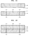
- FIGS. 1A through 1H are cross-sectional views illustrating two silicon substrates and a silicon direct bonding (SDB) method according to an embodiment of the present general inventive concept;
- FIG. 2 is a perspective view illustrating a trench formed on a bonding surface of the silicon substrate and a gas discharge outlet formed to penetrate the silicon substrate in the operation illustrated in FIG. 1H ;
- FIGS. 3A through 3D are cross-sectional views illustrating two silicon substrates and an SDB method according to another embodiment of the present general inventive concept.
- FIGS. 1A through 1H are cross-sectional views illustrating two silicon substrates and a silicon direct bonding (SDB) method according to an embodiment of the present general inventive concept
- FIG. 2 is a perspective view illustrating a trench formed on a bonding surface of the silicon substrate and a gas discharge outlet formed to penetrate the silicon substrate in the operation illustrated in FIG. 1D .
- the SDB method is a method of bonding two silicon substrates 110 and 120 including the following operations.
- first silicon substrate 110 and a second silicon substrate 120 are prepared.
- the first and second silicon substrates 110 and 120 can each be a silicon wafer widely used in the manufacturing of a semiconductor device.
- the first silicon substrate 110 has a first bonding surface 111 and the second silicon substrate 120 has a second bonding surface 121 corresponding to the first bonding surface 111 .
- a photoresist PR 1 is coated on one of the first and second silicon substrates 110 and 120 , for example, on the first bonding surface 111 of the first silicon substrate 110 . Subsequently, the photoresist PR 1 is patterned in a predetermined pattern through an exposure and development process. Then, a part of the first bonding surface 111 of the first silicon substrate 110 is exposed.
- the first bonding surface 111 is etched to a predetermined depth by using the photoresist PR 1 as an etching mask, thereby forming one or more trenches 114 .
- the etching of the first bonding surface 111 can be performed with a dry etching method, such as, for example, a reactive ion etching (RIE), or a wet etching method, such as, for example, submerging for a period of time in a solution such as acetone or the like.
- RIE reactive ion etching
- a wet etching method such as, for example, submerging for a period of time in a solution such as acetone or the like.
- a photoresist PR 2 is again coated on the first bonding surface 111 of the first silicon substrate 110 .
- the photoresist PR 2 is formed to cover the entire pre-formed trench 114 (or trenches).
- the photoresist PR 2 is patterned in a pattern of a plurality of gas discharge outlets on the trench 114 through an exposure and development process.
- a part of the trench 114 (or some of the trenches 114 ) formed on the first bonding surface 111 of the first silicon substrate 110 is exposed and the first silicon substrate 110 under the exposed trench 114 is also exposed, as illustrated in FIG. 1F .
- etching of the first silicon substrate 110 can be made with a dry etching method such as the reactive ion etching (RIE) method or the wet etching method.
- RIE reactive ion etching
- the photoresist PR 2 is stripped, the trench 114 (or trenches) formed to the predetermined depth on the first bonding surface 111 of the first silicon substrate 110 and the gas discharge outlet 118 connected to the trench 114 remain.
- the gas discharge outlet 118 has been formed to penetrate the first silicon substrate 110 .
- the gas discharge outlet 118 may also be formed to penetrate the second silicon substrate 120 .
- the trench 114 may be formed on the first silicon substrate 110 and the gas discharge outlet 118 may be formed in the second silicon substrate 120 to communicate with the corresponding trench 114 .
- the trenches 114 may be formed along a plurality of dicing lines L D1 and L D2 illustrated in FIG. 2 , in order not to affect the semiconductor device formed on the silicon substrates 110 and 120 .
- dicing indicates that, after a plurality of semiconductor devices are formed on the two silicon substrates 110 and 120 , the silicon substrates 110 and 120 are cut so that each of the semiconductor devices can be separated from one another.
- the dicing lines L D1 and L D2 include first lines L D1 that extend to a first direction and second lines L D2 that extend to a second direction perpendicular to the first direction.
- a plurality of trenches 114 may be formed along one of the first lines L D1 and the second lines L D2 , for example, along the first lines L D1 , as illustrated in FIG. 2 .
- a plurality of trenches 116 may alternatively or also be formed on the second lines L D2 .
- the trenches 116 formed along the second lines L D2 may also be formed simultaneously with the trench 114 through the operations illustrated in FIGS. 1A through 1G .
- the trenches 114 and 116 do not extend to the outer circumference of the two silicon substrates 110 and 120 . In other words, both ends of the trenches 114 and 116 are clogged. The clogging of the trenches is performed since when the trenches 114 and 116 extend to the outer circumference of the two silicon substrates 110 and 120 , the possibility that cracks occur on the substrates 110 and 120 may be increased.
- a plurality of gas discharge outlets 118 may be formed on each of the trenches 114 and 116 .
- the gas discharge outlets 118 may be formed in a position in which the first lines L D1 and the second lines L D2 cross one another.
- the gas discharge outlets 118 may be formed simultaneously with a process of forming a through hole when a micro-electro-mechanical system (MEMS) is manufactured. For example, if a process of forming a flow-path through hole is used when an MEMS head for a liquid crystal display (LCD) is manufactured, the gas discharge outlets 118 may also be formed without performing additional processes.
- MEMS micro-electro-mechanical system
- gases generated between the silicon substrates 110 and 120 can be discharged to the outside of the silicon substrates 110 and 120 , which will be described later.
- the cleaning operation can include a cleaning process and a drying process.
- a thin film (not illustrated) formed of ions and molecules such as OH ⁇ , H + , H 2 O, H 2 and O 2 is formed on the first bonding surface 111 of the first silicon substrate 110 and the second bonding surface 121 of the second silicon substrate 120 .
- the two silicon substrates 110 and 120 are pre-bonded with a force (Van der Waals's force) between the above-described ions and the molecules. Subsequently, the two silicon substrates 110 and 120 in the close-contact state are put into a thermal treatment furnace and thermally heated to approximately 1000° C. The two silicon substrates 110 and 120 are then strongly bonded with an inter-diffusion between atoms of the two silicon substrates 110 and 120 .
- gases are generated by the ions and the molecules that exist between the two silicon substrates 110 and 120 .
- the gases can flow into the adjacent trenches 114 and 116 and can be smoothly and easily discharged through the gas discharge outlets 118 that communicate with the trenches 114 and 116 to the outside of the silicon substrates 110 and 120 .
- the gases generated during the thermal treatment process can be smoothly and easily discharged through the trenches 114 and 116 and the gas discharge outlets 118 so that a void is prevented from being formed in the junctions of the two silicon substrates 110 and 120 , or void formation can be minimized.
- FIGS. 3A through 3D are cross-sectional views illustrating two silicon substrates and an SDB method according to another embodiment of the present general inventive concept.
- a silicon oxide film 112 can be formed on one of two silicon substrates 110 and 120 , for example, on the surface of the first silicon substrate 110 .
- the surface of the silicon oxide film 112 is a first bonding surface 111 ′.
- the silicon oxide film 112 can also be formed on a surface 121 corresponding to the second silicon substrate 120 . In this way, if the silicon oxide film 112 is formed on one of the two silicon substrates 110 and 120 or both of them, it is known that a bond strength between the two silicon substrates 110 and 120 is enhanced.
- the silicon oxide film 112 formed on the first silicon substrate 110 is etched to a predetermined depth, thereby forming a trench 114 .
- the trench 116 (or trenches 116 ) illustrated in FIG. 2 can be formed in the silicon oxide film 112 along with the trench 114 (or trenches 114 ).
- the formation of the trenches 114 and 116 can be made with the same method as the method illustrated in FIGS. 1B and 1C .
- the trenches 114 and 116 may be formed to penetrate the entire thickness of the silicon oxide film 112 , as illustrated in FIG. 3B , or may be formed in only a part of the entire thickness of the silicon oxide film 112 .
- the first silicon substrate 110 under the trenches 114 and 116 is etched to be vertically penetrated, thereby forming gas discharge outlets 118 that vertically penetrate the bonding surface 111 ′.
- the formation of the gas discharge outlets 118 can be made with the same method as the method illustrated in FIGS. 1E through 1G . As described above, the gas discharge outlets 118 may be formed to penetrate the second silicon substrate 120 .
- the trenches 114 and 116 may be formed along a plurality of dicing lines L D1 and L D2 illustrated in FIG. 2 , in order not to affect the semiconductor device formed on the silicon substrates 110 and 120 .
- a plurality of trenches 114 may be formed along first lines L D1 that extend to a first direction
- a plurality of trenches 116 may be formed along second lines L D2 that extend to a second direction perpendicular to the first direction.
- the trenches 114 and 116 may be formed in various shapes in which gases can be smoothly and easily discharged according to a bonded area of the silicon substrates 110 and 120 .
- the trenches 114 and 116 do not extend to the outer circumference of the two silicon substrates 110 and 120 . In other words, both ends of the trenches 114 and 116 are clogged.
- a plurality of gas discharge outlets 118 may be formed on each of the trenches 114 and 116 .
- the gas discharge outlets 118 may be formed in a position in which the first lines L D1 and the second lines L D2 cross one another.
- the first silicon substrate 110 and the second silicon substrate 120 are cleaned. Then, as illustrated in FIG. 3D , the first silicon substrate 110 and the second silicon substrate 120 closely contact each other. Subsequently, the two silicon substrates 110 and 120 in the close-contact state are put into a thermal treatment furnace and thermally heated to approximately 1000° C. The two silicon substrates 110 and 120 are then strongly bonded with inter-diffusion between atoms of the two silicon substrates 110 and 120 .
- gases are generated by the ions and the molecules that exist between the two silicon substrates 110 and 120 .
- the gases can flow into the adjacent trenches 114 and 116 and can be smoothly and easily discharged through the gas discharge outlets 118 that communicate with the trenches 114 and 116 to the outside of the silicon substrates 110 and 120 .
- the trench is formed on the bonding surfaces of the two silicon substrates and gases generated during the thermal treatment process can be smoothly and easily discharged through the trenches formed on the boding surface of the two silicon substrates as well as the gas discharge outlets that communicate with the trenches, a void is prevented from being formed in the junctions of the two silicon substrates due to the gases.
- the bond strength of the two silicon substrates is enhanced and the inferiority rate of the semiconductor device formed on the substrates is lowered such that a yield is improved.
Abstract
Description
Claims (17)
Applications Claiming Priority (2)
| Application Number | Priority Date | Filing Date | Title |
|---|---|---|---|
| KR1020050135842A KR20070071965A (en) | 2005-12-30 | 2005-12-30 | Silicon direct bonding method |
| KR2005-135842 | 2005-12-30 |
Publications (2)
| Publication Number | Publication Date |
|---|---|
| US20070155056A1 US20070155056A1 (en) | 2007-07-05 |
| US7442622B2 true US7442622B2 (en) | 2008-10-28 |
Family
ID=38224959
Family Applications (1)
| Application Number | Title | Priority Date | Filing Date |
|---|---|---|---|
| US11/505,420 Active 2026-12-26 US7442622B2 (en) | 2005-12-30 | 2006-08-17 | Silicon direct bonding method |
Country Status (3)
| Country | Link |
|---|---|
| US (1) | US7442622B2 (en) |
| JP (1) | JP4616235B2 (en) |
| KR (1) | KR20070071965A (en) |
Families Citing this family (11)
| Publication number | Priority date | Publication date | Assignee | Title |
|---|---|---|---|---|
| EP2238614B1 (en) * | 2008-01-14 | 2020-03-11 | The Regents of The University of California | Vertical outgassing channels |
| JP2009291514A (en) * | 2008-06-09 | 2009-12-17 | Canon Inc | Method for manufacturing capacitive transducer, and capacitive transducer |
| JP5391599B2 (en) * | 2008-07-14 | 2014-01-15 | オムロン株式会社 | Substrate bonding method and electronic component |
| JPWO2010061470A1 (en) * | 2008-11-28 | 2012-04-19 | セイコーインスツル株式会社 | Manufacturing method of wafer and package product |
| WO2010070753A1 (en) * | 2008-12-18 | 2010-06-24 | セイコーインスツル株式会社 | Wafer and method for manufacturing package product |
| TWI513668B (en) * | 2009-02-23 | 2015-12-21 | Seiko Instr Inc | Manufacturing method of glass-sealed package, and glass substrate |
| JP2012186532A (en) | 2011-03-03 | 2012-09-27 | Seiko Instruments Inc | Wafer, package manufacturing method, and piezoelectric vibrator |
| FR2990054B1 (en) * | 2012-04-27 | 2014-05-02 | Commissariat Energie Atomique | METHOD FOR BONDING IN A GAS ATMOSPHERE HAVING A NEGATIVE JOULE-THOMSON COEFFICIENT |
| FR3001225B1 (en) * | 2013-01-22 | 2016-01-22 | Commissariat Energie Atomique | METHOD FOR MANUFACTURING DIRECT COLLAGE STRUCTURE |
| US9455179B1 (en) | 2015-07-09 | 2016-09-27 | International Business Machines Corporation | Methods to reduce debonding forces on flexible semiconductor films disposed on vapor-releasing adhesives |
| KR20240012544A (en) | 2021-06-30 | 2024-01-29 | 다이킨 고교 가부시키가이샤 | Laminate manufacturing method and laminate |
Citations (3)
| Publication number | Priority date | Publication date | Assignee | Title |
|---|---|---|---|---|
| US4975390A (en) * | 1986-12-18 | 1990-12-04 | Nippondenso Co. Ltd. | Method of fabricating a semiconductor pressure sensor |
| US6124145A (en) * | 1998-01-23 | 2000-09-26 | Instrumentarium Corporation | Micromachined gas-filled chambers and method of microfabrication |
| US6433367B1 (en) * | 1999-07-09 | 2002-08-13 | Oki Data Corporation | Semiconductor device with sloping sides, and electronic apparatus including semiconductor devices with sloping sides, modified for crack-free wire bonding |
Family Cites Families (4)
| Publication number | Priority date | Publication date | Assignee | Title |
|---|---|---|---|---|
| JPH061752B2 (en) * | 1983-12-06 | 1994-01-05 | 株式会社東芝 | Method for joining semiconductor wafers |
| JPH0831608B2 (en) * | 1987-03-25 | 1996-03-27 | 日本電装株式会社 | Method for manufacturing semiconductor pressure sensor |
| JP2001313381A (en) * | 2000-04-28 | 2001-11-09 | Matsushita Electric Ind Co Ltd | Semiconductor wafer and semiconductor device using the same, and method of manufacturing the semiconductor device |
| JP3927925B2 (en) * | 2003-06-04 | 2007-06-13 | 直江津電子工業株式会社 | Semiconductor bonded wafer |
-
2005
- 2005-12-30 KR KR1020050135842A patent/KR20070071965A/en not_active Application Discontinuation
-
2006
- 2006-08-17 US US11/505,420 patent/US7442622B2/en active Active
- 2006-11-02 JP JP2006299519A patent/JP4616235B2/en not_active Expired - Fee Related
Patent Citations (3)
| Publication number | Priority date | Publication date | Assignee | Title |
|---|---|---|---|---|
| US4975390A (en) * | 1986-12-18 | 1990-12-04 | Nippondenso Co. Ltd. | Method of fabricating a semiconductor pressure sensor |
| US6124145A (en) * | 1998-01-23 | 2000-09-26 | Instrumentarium Corporation | Micromachined gas-filled chambers and method of microfabrication |
| US6433367B1 (en) * | 1999-07-09 | 2002-08-13 | Oki Data Corporation | Semiconductor device with sloping sides, and electronic apparatus including semiconductor devices with sloping sides, modified for crack-free wire bonding |
Also Published As
| Publication number | Publication date |
|---|---|
| JP2007184546A (en) | 2007-07-19 |
| KR20070071965A (en) | 2007-07-04 |
| US20070155056A1 (en) | 2007-07-05 |
| JP4616235B2 (en) | 2011-01-19 |
Similar Documents
| Publication | Publication Date | Title |
|---|---|---|
| US7442622B2 (en) | Silicon direct bonding method | |
| US20060138076A1 (en) | Method for making a planar suspended microstructure, using a sacrificial layer of polymer material and resulting component | |
| CN104053105A (en) | Semiconductor Devices and Methods of Forming Thereof | |
| US20060148129A1 (en) | Silicon direct bonding method | |
| US10700262B2 (en) | Piezoelectric device and production method for piezoelectric device | |
| TW516109B (en) | A method of manufacturing semiconductor device and semiconductor device | |
| EP2897170A1 (en) | CMOS integrated method for fabrication of thermopile pixel on semiconductor substrate with buried insulation regions | |
| JP2003188296A (en) | Manufacturing method of semiconductor device | |
| JP2007005401A (en) | Semiconductor device and its manufacturing method | |
| JPH11340317A (en) | Formation of isolation structure | |
| JP6843570B2 (en) | Manufacturing method of semiconductor devices | |
| TW202029289A (en) | Method of fabricating a device comprising a membrane overhanging a cavity | |
| JP2000031262A (en) | Semiconductor device and forming method of shallow trench isolation | |
| TW202040845A (en) | Process for transferring a superficial layer to cavities | |
| US5437739A (en) | Etch control seal for dissolved wafer micromachining process | |
| CN103681309B (en) | Manufacturing method for ultra-thickness metal | |
| JP2009044020A (en) | Semiconductor wafer and method of manufacturing the same | |
| JP2000133817A (en) | Semiconductor pressure sensor and its manufacture | |
| KR20140021415A (en) | Silicon substrate and method preparing the same | |
| JPH1041389A (en) | Manufacture of semiconductor device | |
| US9960081B1 (en) | Method for selective etching using dry film photoresist | |
| US20090166318A1 (en) | Method of Fabricating an Integrated Circuit | |
| US8926848B2 (en) | Through hole forming method | |
| JP6328025B2 (en) | Silicon substrate processing method, liquid discharge head substrate manufacturing method, and liquid discharge head manufacturing method | |
| US6352908B1 (en) | Method for reducing nitride residue in a LOCOS isolation area |
Legal Events
| Date | Code | Title | Description |
|---|---|---|---|
| AS | Assignment |
Owner name: SAMSUNG ELECTRONICS CO., LTD., KOREA, REPUBLIC OF Free format text: ASSIGNMENT OF ASSIGNORS INTEREST;ASSIGNORS:KANG, SUNG-GYU;LIM, SEUNG-MO;LEE, JAE-CHANG;AND OTHERS;REEL/FRAME:018204/0534 Effective date: 20060816 |
|
| STCF | Information on status: patent grant |
Free format text: PATENTED CASE |
|
| FEPP | Fee payment procedure |
Free format text: PAYOR NUMBER ASSIGNED (ORIGINAL EVENT CODE: ASPN); ENTITY STATUS OF PATENT OWNER: LARGE ENTITY |
|
| FEPP | Fee payment procedure |
Free format text: PAYER NUMBER DE-ASSIGNED (ORIGINAL EVENT CODE: RMPN); ENTITY STATUS OF PATENT OWNER: LARGE ENTITY Free format text: PAYOR NUMBER ASSIGNED (ORIGINAL EVENT CODE: ASPN); ENTITY STATUS OF PATENT OWNER: LARGE ENTITY |
|
| FPAY | Fee payment |
Year of fee payment: 4 |
|
| AS | Assignment |
Owner name: SAMSUNG DISPLAY CO., LTD., KOREA, REPUBLIC OF Free format text: ASSIGNMENT OF ASSIGNORS INTEREST;ASSIGNOR:SAMSUNG ELECTRONICS CO., LTD.;REEL/FRAME:029019/0139 Effective date: 20120904 |
|
| FPAY | Fee payment |
Year of fee payment: 8 |
|
| MAFP | Maintenance fee payment |
Free format text: PAYMENT OF MAINTENANCE FEE, 12TH YEAR, LARGE ENTITY (ORIGINAL EVENT CODE: M1553); ENTITY STATUS OF PATENT OWNER: LARGE ENTITY Year of fee payment: 12 |