US7463122B2 - Compact via transmission line for printed circuit board and its designing method - Google Patents
Compact via transmission line for printed circuit board and its designing method Download PDFInfo
- Publication number
- US7463122B2 US7463122B2 US10/558,888 US55888804A US7463122B2 US 7463122 B2 US7463122 B2 US 7463122B2 US 55888804 A US55888804 A US 55888804A US 7463122 B2 US7463122 B2 US 7463122B2
- Authority
- US
- United States
- Prior art keywords
- transmission line
- circuit board
- printed circuit
- via transmission
- compact
- Prior art date
- Legal status (The legal status is an assumption and is not a legal conclusion. Google has not performed a legal analysis and makes no representation as to the accuracy of the status listed.)
- Active, expires
Links
Images


Classifications
-
- H—ELECTRICITY
- H05—ELECTRIC TECHNIQUES NOT OTHERWISE PROVIDED FOR
- H05K—PRINTED CIRCUITS; CASINGS OR CONSTRUCTIONAL DETAILS OF ELECTRIC APPARATUS; MANUFACTURE OF ASSEMBLAGES OF ELECTRICAL COMPONENTS
- H05K1/00—Printed circuits
- H05K1/02—Details
- H05K1/0213—Electrical arrangements not otherwise provided for
- H05K1/0216—Reduction of cross-talk, noise or electromagnetic interference
- H05K1/0218—Reduction of cross-talk, noise or electromagnetic interference by printed shielding conductors, ground planes or power plane
- H05K1/0219—Printed shielding conductors for shielding around or between signal conductors, e.g. coplanar or coaxial printed shielding conductors
- H05K1/0222—Printed shielding conductors for shielding around or between signal conductors, e.g. coplanar or coaxial printed shielding conductors for shielding around a single via or around a group of vias, e.g. coaxial vias or vias surrounded by a grounded via fence
-
- H—ELECTRICITY
- H01—ELECTRIC ELEMENTS
- H01P—WAVEGUIDES; RESONATORS, LINES, OR OTHER DEVICES OF THE WAVEGUIDE TYPE
- H01P3/00—Waveguides; Transmission lines of the waveguide type
- H01P3/02—Waveguides; Transmission lines of the waveguide type with two longitudinal conductors
- H01P3/06—Coaxial lines
-
- H—ELECTRICITY
- H05—ELECTRIC TECHNIQUES NOT OTHERWISE PROVIDED FOR
- H05K—PRINTED CIRCUITS; CASINGS OR CONSTRUCTIONAL DETAILS OF ELECTRIC APPARATUS; MANUFACTURE OF ASSEMBLAGES OF ELECTRICAL COMPONENTS
- H05K1/00—Printed circuits
- H05K1/02—Details
- H05K1/0213—Electrical arrangements not otherwise provided for
- H05K1/0237—High frequency adaptations
- H05K1/024—Dielectric details, e.g. changing the dielectric material around a transmission line
-
- H—ELECTRICITY
- H05—ELECTRIC TECHNIQUES NOT OTHERWISE PROVIDED FOR
- H05K—PRINTED CIRCUITS; CASINGS OR CONSTRUCTIONAL DETAILS OF ELECTRIC APPARATUS; MANUFACTURE OF ASSEMBLAGES OF ELECTRICAL COMPONENTS
- H05K1/00—Printed circuits
- H05K1/02—Details
- H05K1/0213—Electrical arrangements not otherwise provided for
- H05K1/0237—High frequency adaptations
- H05K1/025—Impedance arrangements, e.g. impedance matching, reduction of parasitic impedance
- H05K1/0251—Impedance arrangements, e.g. impedance matching, reduction of parasitic impedance related to vias or transitions between vias and transmission lines
-
- H—ELECTRICITY
- H05—ELECTRIC TECHNIQUES NOT OTHERWISE PROVIDED FOR
- H05K—PRINTED CIRCUITS; CASINGS OR CONSTRUCTIONAL DETAILS OF ELECTRIC APPARATUS; MANUFACTURE OF ASSEMBLAGES OF ELECTRICAL COMPONENTS
- H05K2201/00—Indexing scheme relating to printed circuits covered by H05K1/00
- H05K2201/01—Dielectrics
- H05K2201/0183—Dielectric layers
- H05K2201/0187—Dielectric layers with regions of different dielectrics in the same layer, e.g. in a printed capacitor for locally changing the dielectric properties
-
- H—ELECTRICITY
- H05—ELECTRIC TECHNIQUES NOT OTHERWISE PROVIDED FOR
- H05K—PRINTED CIRCUITS; CASINGS OR CONSTRUCTIONAL DETAILS OF ELECTRIC APPARATUS; MANUFACTURE OF ASSEMBLAGES OF ELECTRICAL COMPONENTS
- H05K2201/00—Indexing scheme relating to printed circuits covered by H05K1/00
- H05K2201/09—Shape and layout
- H05K2201/09009—Substrate related
- H05K2201/09063—Holes or slots in insulating substrate not used for electrical connections
-
- H—ELECTRICITY
- H05—ELECTRIC TECHNIQUES NOT OTHERWISE PROVIDED FOR
- H05K—PRINTED CIRCUITS; CASINGS OR CONSTRUCTIONAL DETAILS OF ELECTRIC APPARATUS; MANUFACTURE OF ASSEMBLAGES OF ELECTRICAL COMPONENTS
- H05K2201/00—Indexing scheme relating to printed circuits covered by H05K1/00
- H05K2201/09—Shape and layout
- H05K2201/09209—Shape and layout details of conductors
- H05K2201/095—Conductive through-holes or vias
- H05K2201/09536—Buried plated through-holes, i.e. plated through-holes formed in a core before lamination
-
- H—ELECTRICITY
- H05—ELECTRIC TECHNIQUES NOT OTHERWISE PROVIDED FOR
- H05K—PRINTED CIRCUITS; CASINGS OR CONSTRUCTIONAL DETAILS OF ELECTRIC APPARATUS; MANUFACTURE OF ASSEMBLAGES OF ELECTRICAL COMPONENTS
- H05K2201/00—Indexing scheme relating to printed circuits covered by H05K1/00
- H05K2201/09—Shape and layout
- H05K2201/09209—Shape and layout details of conductors
- H05K2201/095—Conductive through-holes or vias
- H05K2201/09618—Via fence, i.e. one-dimensional array of vias
-
- H—ELECTRICITY
- H05—ELECTRIC TECHNIQUES NOT OTHERWISE PROVIDED FOR
- H05K—PRINTED CIRCUITS; CASINGS OR CONSTRUCTIONAL DETAILS OF ELECTRIC APPARATUS; MANUFACTURE OF ASSEMBLAGES OF ELECTRICAL COMPONENTS
- H05K2201/00—Indexing scheme relating to printed circuits covered by H05K1/00
- H05K2201/09—Shape and layout
- H05K2201/09209—Shape and layout details of conductors
- H05K2201/09654—Shape and layout details of conductors covering at least two types of conductors provided for in H05K2201/09218 - H05K2201/095
- H05K2201/09718—Clearance holes
-
- H—ELECTRICITY
- H05—ELECTRIC TECHNIQUES NOT OTHERWISE PROVIDED FOR
- H05K—PRINTED CIRCUITS; CASINGS OR CONSTRUCTIONAL DETAILS OF ELECTRIC APPARATUS; MANUFACTURE OF ASSEMBLAGES OF ELECTRICAL COMPONENTS
- H05K2201/00—Indexing scheme relating to printed circuits covered by H05K1/00
- H05K2201/09—Shape and layout
- H05K2201/09209—Shape and layout details of conductors
- H05K2201/09654—Shape and layout details of conductors covering at least two types of conductors provided for in H05K2201/09218 - H05K2201/095
- H05K2201/09809—Coaxial layout
-
- H—ELECTRICITY
- H05—ELECTRIC TECHNIQUES NOT OTHERWISE PROVIDED FOR
- H05K—PRINTED CIRCUITS; CASINGS OR CONSTRUCTIONAL DETAILS OF ELECTRIC APPARATUS; MANUFACTURE OF ASSEMBLAGES OF ELECTRICAL COMPONENTS
- H05K3/00—Apparatus or processes for manufacturing printed circuits
- H05K3/40—Forming printed elements for providing electric connections to or between printed circuits
- H05K3/42—Plated through-holes or plated via connections
- H05K3/429—Plated through-holes specially for multilayer circuits, e.g. having connections to inner circuit layers
Definitions
- the present invention relates to a compact via transmission line for a printed circuit board and a design method of the same, and in particular to a miniaturized compact via transmission line for a printed circuit board in which constitutive parameters of medium filling the clearance hole of the via transmission line such as relative permittivity and relative permeability are different from the constitutive parameter of an insulating layer comprising the printed circuit board, and a design method of the same.
- Interconnected circuits are very important for improvement in speeding up and packing density of a digital device and a communication device, and have a great effect on the electric characteristics of these devices.
- a printed circuit board including a multilayer board is cost-effective and convenient interconnect technology in which conductor layers which are mutually insulated by insulating layers are used for ground, power supply, and signals. This technology is particularly important in development and design of an interconnected circuit such as a planar transmission line including a micro-strip line, a strip line, a coplanar line, and a slot line as well as via transmission lines.
- a coaxial line of predetermined impedance is formed to reduce a signal attenuation by forming the coaxial line of the predetermined impedance from a metal plate, an insulator, and a metal pin on a printed circuit board to permit the passage of a high-frequency signal therethrough is disclosed in, for example, the Japanese Unexamined Patent Publication No. 6(1994)-104601.
- via holes for shielding electromagnetic waves are arranged on all sides so that the distance between each via hole is less than 1 ⁇ 2 of an effective wavelength to prevent the occurrence of resonance is disclosed in, for example, the Japanese Unexamined Patent Publication No. 2001-68596.
- a typical example of an interconnection in a direction perpendicular to a printed circuit board includes a via hole structure.
- Simple via holes formed on the printed circuit board produce parasitic oscillation in an insulating layer comprising the printed circuit board to generate unnecessary electromagnetic radiation from the printed circuit board. For this reason, as described in Patent Document 3, the method using the ground via hole as the barrier is being carried out to avoid the effects of such unnecessary radiation.
- a first aspect of the present invention is a compact via transmission line for a printed circuit board provided on the printed circuit board, wherein said compact via transmission line comprises a central conductor which forms an inner conductor boundary of said compact via transmission line, and through which a signal transmits, a plurality of ground via holes which form an outer conductor boundary of said compact via transmission line, a ground plate formed of a conductor layer of said printed circuit board connected to said ground via holes, and a constitutive parameter adjustment via hole provided between said inner conductor boundary and said outer conductor boundary to adjust a constitutive parameter of said printed circuit board, and wherein said constitutive parameter adjustment via hole is filled with a uniform medium or a composite medium having a second constitutive parameter different from a first constitutive parameter of an insulating layer comprising said printed circuit board.
- said printed circuit board be a multilayer printed circuit board having a plurality of conductor layers.
- said first and second constitutive parameters be at least any one of relative permittivity and relative permeability.
- said compact via transmission line be impedance-matched to an interconnected circuit mounted on said printed circuit board and connected to said compact via transmission line.
- Said ground via holes may be arranged on a circumference, said ground via holes may also be arranged in a square.
- a second aspect of the present invention is a compact via transmission line for a printed circuit board provided on the printed circuit board, wherein said compact via transmission line comprises a central conductor which forms an inner conductor boundary of said compact via transmission line, and through which a signal transmits, a plurality of ground via holes which form an outer conductor boundary of said compact via transmission line, a ground plate formed of a conductor layer of said printed circuit board connected to said ground via holes, a constitutive parameter adjustment via hole provided between said inner conductor boundary and said outer conductor boundary to adjust a constitutive parameter of said printed circuit board, and air vents provided between said inner conductor boundary and said outer conductor boundary so as to excavate said printed circuit board.
- said air vents be provided on said printed circuit board so as to adjust the characteristic impedance of a via transmission line provided on said printed circuit board and an interconnected circuit connected to the via transmission line.
- Said air vents may have of at least two different sized round shapes.
- Said air vents may be irregularly arranged between said inner conductor boundary and said outer conductor boundary.
- Said air vents may be arranged to be symmetric with respect to said signal via hole.
- the maximum length of the cross-sectional shapes of said air vents be not more than 1 ⁇ 8 of the minimum wavelength in a predetermined frequency range of a signal propagating through an insulating layer of said printed circuit board.
- Said ground via holes may be arranged on a circumference, said ground via holes may also be arranged in a square.
- the electric field and the magnetic field of a principal electromagnetic wave propagating on said printed circuit board be in a direction perpendicular to a propagation direction, the electric field and the magnetic field being at right angles to each other.
- a third aspect of the present invention is a compact via transmission line for a printed circuit board provided on the printed circuit board, wherein said compact via transmission line comprises two central conductors which form two inner conductor boundaries of said compact via transmission line, and through which differential signals transmit, a plurality of ground via holes which form two outer conductor boundaries each arranged around said two central conductors, ground plates formed of conductor layers of said printed circuit board connected to said ground via holes, and two constitutive parameter adjustment via holes provided between said two inner conductor boundaries and said two outer conductor boundaries to adjust constitutive parameters of said printed circuit board, and wherein said two constitutive parameter adjustment via holes are each filled with a uniform medium or a composite medium having a second constitutive parameter different from a first constitutive parameter of an insulating layer comprising said printed circuit board.
- a fourth aspect of the present invention is a design method of a compact via transmission line for a printed circuit board comprising a central conductor which forms an inner conductor boundary of the compact via transmission line for the printed circuit board provided on the printed circuit board, and through which a signal transmits, a plurality of ground via holes which form an outer conductor boundary of said compact via transmission line, and a ground plate formed of a conductor layer of said printed circuit board connected to the ground via holes, wherein a constitutive parameter adjustment via hole for adjusting a constitutive parameter of said printed circuit board is provided between said inner conductor boundary and said outer conductor boundary, said constitutive parameter adjustment via hole being filled with a uniform medium or a composite medium having a second constitutive parameter different from a first constitutive parameter of an insulating layer comprising said printed circuit board.
- said first and second constitutive parameters be at least any one of relative permittivity and relative permeability.
- said compact via transmission line be impedance-matched to an interconnected circuit mounted on said printed circuit board and connected to said compact via transmission line.
- a fifth aspect of the present invention is a design method of a compact via transmission line for a printed circuit board comprising a central conductor which forms an inner conductor boundary of the compact via transmission line for the printed circuit board provided on the printed circuit board, and through which a signal transmits, a plurality of ground via holes which form an outer conductor boundary of said compact via transmission line, and a ground plate formed of a conductor layer of said printed circuit board connected to the ground via holes, wherein a constitutive parameter adjustment via hole for adjusting a constitutive parameter of said printed circuit board is provided between said inner conductor boundary and said outer conductor boundary, and air vents are further formed between said inner conductor boundary and said outer conductor boundary so as to excavate said printed circuit board.
- said air vents be provided on said printed circuit board so as to adjust the characteristic impedance of a via transmission line provided on said printed circuit board and an interconnected circuit connected to the via transmission line.
- the electric field and the magnetic field of a principal electromagnetic wave propagating on said printed circuit board be in a direction perpendicular to a propagation direction, the electric field and the magnetic field being at right angles to each other.
- the maximum length of the cross-sectional shapes of said air vents be not more than 1 ⁇ 8 of the minimum wavelength in a predetermined frequency range of a signal propagating through an insulating layer of said printed circuit board.
- FIG. 1A is a plan view showing a compact via transmission line according to the invention of the present application in a printed circuit board;
- FIG. 1B is a longitudinal sectional view showing the compact via transmission line according to the invention of the present application in the printed circuit board;
- FIG. 2A is a plan view showing a compact via transmission line according to the invention of the present application in which ground via holes are arranged on a circumference in a printed circuit board;
- FIG. 2B is a longitudinal sectional view showing the compact via transmission line according to the invention of the present application in which the ground via holes are arranged on a circumference in the printed circuit board;
- FIG. 3A is a plan view showing a compact via transmission line according to the invention of the present application in which ground via holes are arranged in a square in a printed circuit board;
- FIG. 3B is a longitudinal sectional view showing the compact via transmission line according to the invention of the present application in which the ground via holes are arranged in a square in the printed circuit board;
- FIG. 4A is a plan view showing a compact via transmission line according to the invention of the present application in which air vents are formed in the area of a constitutive parameter adjustment via hole of the compact via transmission line in a printed circuit board;
- FIG. 4B is a longitudinal sectional view showing the compact via transmission line according to the invention of the present application in which the air vents are formed in the area of the constitutive parameter adjustment via hole of the compact via transmission line in the printed circuit board;
- FIG. 5A is a plan view showing a compact via transmission line according to the invention of the present application having air vents formed between a central conductor and ground via holes, and provided with a constitutive parameter adjustment via hole and conductor plates forming ground layers of a printed circuit board in the printed circuit board;
- FIG. 5B is a longitudinal sectional view showing the compact via transmission line according to the invention of the present application having the air vents formed between the central conductor and the ground via holes, and provided with the constitutive parameter adjustment via hole and the conductor plates forming the ground layers of the printed circuit board in the printed circuit board;
- FIG. 6A is a plan view showing a compact via transmission line according to the invention of the present application in which round-shaped and different-sized air vents are formed in a printed circuit board;
- FIG. 6B is a longitudinal sectional view showing the compact via transmission line according to the invention of the present application in which the round-shaped and different-sized air vents are formed in the printed circuit board;
- FIG. 7 is a plan view showing a compact via transmission line according to the invention of the present application in which square and rectangular air vents are formed;
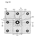
- FIG. 8 is a plan view showing a compact via transmission line according to the invention of the present application in which air vents are arranged according to a predetermined criterion;
- FIG. 9 is a plan view showing a compact via transmission line according to the invention of the present application in which air vents are irregularly arranged;
- FIG. 10A is a plan view showing an interconnected circuit from a compact via transmission line to a strip line according to the invention of the present application in a printed circuit board;
- FIG. 10B is a longitudinal sectional view showing the interconnected circuit from the compact via transmission line to the strip line according to the invention of the present application in the printed circuit board;
- FIG. 11A is a plan view showing an interconnected circuit from a compact via transmission line to a micro-strip line according to the invention of the present application in a printed circuit board;
- FIG. 11B is a longitudinal sectional view showing the interconnected circuit from the compact via transmission line to the micro-strip line according to the invention of the present application in the printed circuit board;
- FIG. 12 is a plan view showing two primitive cells forming a compact via transmission line according to the invention of the present application, as well as having a composite via hole structure for connecting each cell to two strip lines in order to transmit a differential signal;
- FIG. 13 is a plan view showing a via hole structure under an SMA connector in which a compact via transmission line according to the invention of the present application is formed and connected to a strip line in a printed circuit board;
- FIG. 14A is a plan view showing a compact via transmission line according to the invention of the present application in which ground via holes are arranged on a circumference, and in which a central conductor, ground via holes, a constitutive parameter adjustment via hole, and a filling medium are formed part of the way from a surface of a multilayer printed circuit board in a printed circuit board;
- FIG. 14B is a longitudinal sectional view showing the compact via transmission line according to the invention of the present application in which the ground via holes are arranged on a circumference, and in which the central conductor, the ground via holes, the constitutive parameter adjustment via hole and the filling medium are formed part of the way from a surface of a multilayer printed circuit board in a printed circuit board;
- FIG. 15A is a plan view showing a compact via transmission line according to the invention of the present application in which air vents are formed in the area of a constitutive parameter adjustment via hole of the compact via transmission line, and in which a central conductor, ground via holes, the constitutive parameter adjustment via hole, and a filling medium are formed part of the way from a surface of a multilayer printed circuit board in a printed circuit board;
- FIG. 15B is a longitudinal sectional view showing the compact via transmission line according to the invention of the present application in which the air vents are formed in the area of the constitutive parameter adjustment via hole of the compact via transmission line, and in which the central conductor, the ground via holes, the constitutive parameter adjustment via hole, and the filling medium are formed part of the way from a surface of a multilayer printed circuit board in a printed circuit board;
- FIG. 16A is a diagram showing simulation results of a reflection coefficient with respect to a usual via transmission line mounted on a multilayer board formed with 12 conductor layers and a compact via transmission line according to the present invention
- FIG. 16B is a diagram showing simulation results of a transmission coefficient with respect to the usual via transmission line mounted on the multilayer board formed with 12 conductor layers and the compact via transmission line according to the present invention
- FIG. 17A is a diagram showing simulation results of a reflection coefficient with respect to a usual via transmission line mounted an a multilayer board formed with 12 conductor layers and a compact via transmission line according to the present invention
- FIG. 17B is a diagram showing simulation results of a transmission coefficient with respect to the usual via transmission line mounted on the multilayer board formed with 12 conductor layers and the compact via transmission line according to the present invention
- FIG. 18A is a diagram showing simulation results of a reflection coefficient with respect to a usual via transmission line mounted on a multilayer board formed with 12 conductor layers and a compact via transmission line according to the present invention.
- FIG. 18B is a diagram showing simulation results of a transmission coefficient with respect to the usual via transmission line mounted on the multilayer board formed with 12 conductor layers and the compact via transmission line according to the present invention.
- the compact via transmission line has a central conductor which forms an inner conductor layer boundary of the compact via transmission line, a plurality of ground via holes arranged around the signal via and a set of ground plates from conductor layers of a printed circuit board to form an outer conductor boundary of the compact via transmission line, and a constitutive parameter adjustment via hole for electrically isolating the inner conductor boundary from the outer conductor boundary which have differential potentials.
- This constitutive parameter adjustment via hole may be filled with a composite material made of a uniform substance or a plurality of different substances.
- a particular example includes a method of forming air vents between a signal via and ground via holes of a via transmission line to adjust a constitutive parameter of a printed circuit board.
- a filling medium for filling the constitutive parameter adjustment via hole of the present invention is usually selected in such a way that the characteristic impedance of this compact via transmission line and a circuit mounted on a printed circuit board and connected to the compact via transmission line is matched along with miniaturization of the printed circuit board.
- the printed circuit board may be miniaturized by selecting so that either or both constitutive parameters of a medium material having filled the constitutive parameter adjustment via hole, or either or both relative permittivity and relative permeability of the air vents differ from constitutive parameters corresponding to an insulating layer comprising the printed circuit board, thus allowing packing density to be improved.
- the printed circuit board using the via transmission line of the present invention is operable at a wide frequency band, so that a high-speed digital signal can be transmitted.
- any number of the compact via transmission lines in which via holes are arranged in a complicated and high density state may be used to connect any kinds of interconnected circuits such as planar transmission lines.
- the compact via transmission line according to the invention of the present application is also applicable to a multilayer printed circuit board having any transmission lines.
- FIG. 1A and FIG. 1B are a plan view and a longitudinal sectional view showing the compact via transmission line according to the invention of the present application in a printed circuit board.
- FIG. 1A and FIG. 1B there is shown an example of the compact via transmission line formed on a multilayer printed circuit board made up of conductor layers 1 to 10 with 10 layers as a design example of the multilayer printed circuit board.
- Ground lines 107 , signal lines 108 , and power supply lines 109 are formed by the conductor layers 1 to 10 insulated by insulating layers 105 in the multilayer printed circuit board.
- the compact via transmission line comprises a central conductor 101 , ground via holes 102 arranged around the central conductor 101 , ground plates 106 from the conductor layers 106 , and a constitutive parameter adjustment via hole 103 having a diameter of dcle filled with a filling medium 104 .
- Constitutive parameters of the filling medium 104 for example, either or both of the relative permittivity and the relative permeability are selected so as to differ from corresponding constitutive parameters of insulating layers 105 in order to satisfy both of the miniaturization and characteristic impedance matching to an interconnected circuit.
- the energy of an electromagnetic wave signal incoming from a circuit linked to the compact via transmission line will be partially returned by reflection in the linked point, but the reflection may be extremely reduced by adjusting the dimension of the compact via transmission line, and either or both of the values of the relative permittivity and the relative permeability, thereby making it possible to transmit a signal with little or no attenuation of signal amplitude.
- this via transmission line may be considered as well enough insulated transmission line.
- the outer boundary of the via transmission line including the ground via holes may also be considered as the boundary formed of approximately continuous conductor surface.
- the characteristic impedance of the via transmission line may be calculated at a good approximation by regarding the inner and outer boundaries formed of the continuous conductor surfaces as in corresponding coaxial transmission line, and a signal wave as traveling along these boundaries.
- FIG. 2A and FIG. 2B are a plan view and a longitudinal sectional view showing the compact via transmission line according to the invention of the present application, in which ground via holes are arranged on a circumference in a printed circuit board.
- the basic structure of the via transmission line shown in FIG. 2A and FIG. 2B are identical to the structure shown in FIG. 1A and FIG. 1B except that ground via holes 202 are arranged on a circumference with a focus on a central conductor 201 , and yet at even intervals.
- the characteristic impedance of this via transmission line may be approximated by the following well-known (1) formula used when a signal wave travels between continuous inner and outer conductor boundaries on a circumference:
- Zr is the characteristic impedance of the via transmission line
- R r Dr/2 being the distance between the center of the ground via hole and the center of the central conductor
- r rod d rod/2 being the radius of the central conductor
- ⁇ is the relative permittivity of the insulating layers 205
- the relative permeability of insulating material 205 is equal to 1.
- the relative permittivity of the filing medium 204 for filling the constitutive parameter adjustment via hole 203 with a diameter of d cle differs from the relative permittivity of the insulating layers 205 comprising the printed circuit board.
- the characteristic impedance of the via transmission line mounted on the printed circuit board is calculated based on effective relative permittivity determined from both of the relative permittivity of the filling medium 204 having filled the constitutive parameter adjustment via hole 203 and the relative permittivity of the insulating layers 205 of the printed circuit board.
- This effective relative permittivity is found by well-known theory and experimental methods. If the relative permittivity of the filling medium 204 having filled the constitutive parameter adjustment via hole of the compact via transmission line is smaller than the relative permittivity of the insulating layers 205 , the effective relative permittivity of the via transmission line becomes smaller than the relative permittivity of the insulating layers 205 .
- the cross-sectional area of the compact via transmission line according to the invention of the present application becomes smaller than the cross-sectional area of the via transmission line in which the materials of the filling medium 204 and the insulating layers 205 are identical since the characteristic impedance of the two via transmission lines are equal, and yet parameters other than the filling medium having filled the constitutive parameter adjustment via hole are equal.
- the characteristic impedance of the compact via transmission line in which the ground via holes 202 shown in FIG. 2A and FIG. 2B are arranged a circumference is represented by the following (2) formula.
- ZCVT,r is the characteristic impedance of the compact via transmission line, ⁇ eff being effective relative permittivity determined from both of the insulating layers 205 and the filling medium 204 having filled the constitutive parameter adjustment via hole.
- FIG. 3A and FIG. 3B are a plan view and a cross-sectional view showing a compact via transmission line in a printed circuit board, in which ground via holes 302 are arranged in a square around a central conductor 301 .
- the compact via transmission line is shown as if it was incorporated into the printed circuit board in a manner similar to FIG. 1A and FIG. 1B for convenience of explanation.
- the characteristic impedance of a via transmission line may be approximated by the following well-known (3) formula used when a signal wave travels between the inner conductor boundary and outer square-continued conductor boundary.
- Z sq is the characteristic impedance of the compact via transmission line
- ⁇ is the relative permittivity of insulating layers 305 , with the relative permeability of the insulating layers 305 as 1.
- the relative permittivity of a filling medium 304 filling the constitutive parameter adjustment via hole 303 be made smaller than the relative permittivity of the insulating layers 305 insulating the conductor layers of the printed circuit board in order to form the compact via transmission line on the printed circuit board.
- the characteristic impedance of the compact via transmission line in which the ground via holes shown in FIG. 3A and FIG. 3B are arranged in a square is represented by the following (4) formula.
- ZCVT,r is the characteristic impedance of the compact via transmission line, ⁇ eff being effective relative permittivity determined from both of the insulating layers 305 and the filling medium 304 having filled the constitutive parameter adjustment via hole.
- Tile conclusion from the consideration for the compact via transmission line using the ground via holes arranged in a square is identical to the conclusion obtained from the compact via transmission line using the ground via holes arranged on a circumference. More specifically, it is possible to miniaturize the compact via transmission line by reducing the relative permittivity of the filling medium filling the constitutive parameter adjustment via hole. In this way, the aforementioned two embodiments are based on design concept that the ground via holes are formed around the central conductor, and formed so that the filling medium filling the constitutive parameter adjustment via hole differs from the insulating materials for insulating the conductor layers of the printed circuit board.
- a particular and very important method in forming a composite medium is the one using air vents to form the filling medium filling the constitutive parameter. This is because the composite medium using the air vents is suitable for use in comprising the compact via transmission line from the fact that the relative permittivity and the relative permeability of air are virtually 1.
- FIG. 4A and FIG. 4B are each a plan view and a cross-sectional view showing a compact via transmission line having ground via holes 402 arranged in a square around a central conductor 401 .
- a composite insulator 404 having filled a constitutive parameter adjustment via hole 403 is formed so that the relative permittivity of the composite insulator 404 is smaller than the relative permittivity of insulating layers 405 for insulating the conductor layers of the printed circuit board, and in which air vents are provided so as to excavate the insulating layers 405 in the area of the constitutive parameter adjustment via hole 403 in structure.
- the conductor layer arrangement of the printed circuit board has the same structure as those shown in FIG. 1A and FIG. 1B .
- Air vents 410 provided so as to excavate the insulating layers 405 form such a composite medium of the constitutive parameter adjustment via hole 403 that the relative permittivity thereof can be regarded as being effectively smaller than the relative permittivity of the insulating layers 405 of the printed circuit board.
- the effective relative permittivity of the composite medium of the constitutive parameter adjustment via hole 403 is dependent on the volume occupied by the air vents 410 , and is found from well-known theory and experiment results.
- the composite medium formed of the air vents and the insulating materials of the printed circuit board makes it possible to comprise the compact via transmission line according to the invention of the present application, the cross-sectional area of which is reduced.
- higher-order modes in the compact via transmission line will be establish at higher frequencies due to reducing the effective permittivity and the distance to ground via holes forming the outer conductor boundary of the compact via transmission line. This allows the operating frequency range of the compact via transmission line to be enlarged.
- the air vents of the compact via transmission line mounted on the printed circuit board improves air circulation in air-cooling, thereby enabling heat radiation characteristics in high-density mounting to be improved.
- a fundamental wave of electromagnetic waves is mainly present between the central conductor and the ground via holes making up the outer conductor boundary in the compact via transmission line, so that the air vents may be formed not only in the area of the constitutive parameter adjustment via hole, but also in all area between the central conductor and the ground via holes.
- FIG. 5A and FIG. 5B each have air vents formed between a central conductor and ground via holes, and are a plan view and a cross-sectional view showing a compact via transmission line in a printed circuit board.
- Air vents 510 are formed in the area of the constitutive parameter adjustment via hole 503 , and in the area between the constitutive parameter adjustment via hole 503 and the ground via holes 502 as to excavate conductive plates 506 from conductive layers 507 .
- the cross-section of the air vents in the compact via transmission line may be any shape and any size, but requires to be considerably smaller than the wavelength ⁇ of a propagation signal traveling through insulating layers 505 for insulating the conductor layers of the printed circuit board, for example, 1 ⁇ /8.
- 1 is the maximum dimension in the cross-section of the air vents, ⁇ being the minimum wavelength of the propagation signal in the insulating layer of the printed circuit board in a predetermined frequency range.
- FIG. 6A and FIG. 6B are a plan view and a longitudinal sectional view showing the compact via transmission line according to the invention of the present application, in which round-shaped and different-sized air vents are formed in a printed circuit board.
- cylindrical-shaped air vents with a diameter of da 1 and a diameter of da 2 are each arranged between a central conductor 601 and ground via holes 602 forming a square outer conductor boundary.
- FIG. 7 is a plan view showing the compact via transmission line according to the invention of the present application, in which square and rectangular air vents are formed.
- horizontal cross-sectional shapes of air vents 710 are square and rectangular, and have different size in rectangular shapes and square shapes as illustrated.
- FIG. 7 does not show a longitudinal cross-sectional view, but shows the same structure as the structure of the longitudinal sectional view shown in FIG. 5B . More specifically, the air vents 710 have the horizontal cross-sectional shapes with the square and rectangular cylindrical structure shown in FIG. 7 .
- FIG. 8 shows a concrete example of a compact via transmission line in which air vents 810 are arranged in accordance with the predetermined rule.
- Ground via holes 802 forming the outer conductor boundary of the compact via transmission line are arranged on a circumference around a central conductor 801 so that each distance from the central conductor 801 is equal.
- the air vents 810 are arranged around the central conductor 801 so that each distance of adjacent air vents is equal, and further each distance from the central conductor 801 is equal.
- FIG. 9 is a plan view showing a compact via transmission line in which air vents 910 are irregularly arranged between a central conductor 901 and ground via holes 902 forming an outer conductor boundary.
- a method of forming air vents in a compact via transmission line includes a wide variety of methods, such as a method of forming a hole in a mechanical fashion, and a method of forming a hole using a laser beam.
- FIG. 10A and FIG. 10B show a concrete example in which a compact via transmission line is connected to a planar transmission line as a strip line 1011 in a multilayer printed circuit board with 12 layers.
- the compact via transmission line has a central conductor 1001 , ground via holes 1002 arranged in a square, ground plates 1006 formed of conductor layers 1007 comprising the printed circuit board, and a constitutive parameter adjustment via hole 1003 .
- a composite medium in the compact via transmission line is formed of insulating layers 1005 for insulating conductor layers of the printed circuit board, and air vents 1010 formed differently in size between the central conductor 1001 and the ground via holes 1002 of the compact via transmission line in accordance with the predetermined rule.
- four large air vents are arranged so that each distance of the adjacent air vents is equal, and is evenly arranged around the central conductor 1001 , while three small air vents are evenly arranged around the central conductor 1001 between the adjacent large air vents.
- all the air vents are arranged to be symmetric with respect to the horizontal axis of the strip line 1011 .
- the effective relative permittivity of the composite medium in the compact via transmission line is smaller than the relative permittivity of the insulating layers 1005 , thus making it possible to miniaturize a transmission line connected to the strip line 1011 , while maintaining the characteristic impedance of the strip line 1011 at the same value.
- FIG. 11A and FIG. 11B show a concrete example in which a compact via transmission line is connected to a planar transmission line as a micro-strip line 1112 in a multilayer printed circuit board with 12 layers.
- the compact via transmission line has a central conductor 1101 , ground via holes 1102 arranged on a circumference, ground plates 1106 formed of conductor layers 1107 comprising a printed circuit board, and a constitutive parameter adjustment via hole 1103 .
- a composite medium in the compact via transmission line is formed of insulating layers 1105 for insulating conductor layers of the printed circuit board, and air vents 1110 arranged irregularly between the central conductor 1101 and the ground via holes 1102 of the compact via transmission line except for the area of the micro-strip line 1112 .
- the effective relative permittivity of the composite medium in the compact via transmission line is smaller than the relative permittivity of the insulating layers 1105 , thus making it possible to miniaturize a transition to the micro-strip line 1112 , while maintaining the characteristic impedance of the micro-strip line 1112 at the same value.
- FIG. 12 shows an example of a compact via transmission line for transmitting a differential signal, in which two primitive cells for a high-density via hole structure are shown. These two primitive cells make up a signal via hole pair, and are each connected to a strip line pair as an example of a planar transmission line.
- the compact via transmission line comprises two signal via holes 1201 each surrounded by ground via holes 1202 , ground layers formed of conductor layers, and two constitutive parameter adjustment via holes 1203 .
- Air vents 1210 are formed for the purpose of obtaining the characteristic impedance matching of the compact via transmission line to the strip line pair.
- FIG. 13 is a plan view showing a via hole structure under an SMA (sub-miniature-type-A) connector which is an applied example of a compact via transmission line.
- a usual SMA connector pin is provided with a central conductor 1301 and ground via holes 1313 . Connection of a strip line 1311 as an example of a planar transmission line structure to the central conductor 1301 is shown a gain in said FIG. 3 .
- a usual via transmission line produces a large radiation and leakage losses at high frequencies, and is subject to restrictions of an operating frequency range caused by higher-order modes dependent on the distance to the ground via holes 1313 .
- the compact via transmission line has a central conductor 1301 , ground via holes 1302 arranged on a circumference, ground plates from conductor layers of a printed circuit board, and a constitutive parameter adjustment via hole 1303 .
- a composite medium is formed by excavating air vents 1310 in insulating layers.
- the distance between the central conductor 1301 and the ground via holes 1302 , and the number and the size of the air vents 1310 are defined so that the characteristic impedance is optimized in an interconnected circuit including the SMA connector and the strip line. And, its structure is such that only the electromagnetic wave of a fundamental mode mainly propagates in a predetermined frequency range.
- the electric field and the magnetic field of a principal electromagnetic wave propagating on the printed circuit board is in a direction perpendicular to a propagation direction, and are set so that the electric field and the magnetic field are at right angles to each other for propagation, provided that an electromagnetic wave propagating on an actual printed circuit board includes not only the electromagnetic wave of the fundamental mode described above, but also such an electromagnetic wave that the electric field and the electromagnetic field are deviated from a direction perpendicular to a propagation direction, and are not at right angles to each other.
- the invention of the present application is similarly applicable to this case.
- the central conductor, the ground via holes, the constitutive parameter adjustment via hole, and the filling media are provided so as to penetrate from a surface to a rear surface of the multilayer printed circuit board, but are not necessarily required to penetrate therethrough. It is possible to form part or all of the central conductor, the ground via holes, the constitutive parameter adjustment via hole, and the filling medium ranging from the surface of the multilayer printed circuit board to an internal board comprising the multilayer printed circuit board.
- FIG. 14A and FIG. 14B are a plan view and a cross-sectional view showing the compact via transmission line according to the invention of the present application, in which ground via holes 1402 are each arranged on a circumference, and a central conductor 1401 , the ground via holes 1402 , a constitutive parameter adjustment via hole 1403 , and a filling medium 1404 are formed part of the way from a surface of a multilayer printed circuit board in a printed circuit board.
- the central conductor 201 , the ground via holes 202 , the constitutive parameter adjustment via hole 203 , and the filling medium 204 are provided so as to penetrate from the surface to the rear surface of the multilayer printed circuit board.
- the central conductor 1401 is formed from a first layer which is a top surface layer to a third layer, and the ground via holes 1402 , the constitutive parameter adjustment via hole 1403 , and the filling medium 1404 are formed from the first layer which is the top surface layer to a fourth layer.
- FIG. 15A and FIG. 15B are a plan view and a cross-sectional view showing the compact via transmission line according to the invention of the present application, in which air vents are formed in the area of a constitutive parameter adjustment via hole of a compact via transmission line, and a central conductor 1501 , ground via holes 1502 , a constitutive parameter adjustment via hole 1503 , and air vents 1510 are formed part of the way from a surface of a multilayer printed circuit board, respectively.
- the structure of the present embodiment shown in FIG. 15A and FIG. 15B is similar to the structure shown in FIG. 4A and FIG. 4B except for the following points. According to the present embodiment shown in FIG. 15A and FIG.
- the central conductor 1501 is formed from a first layer which is a top surface layer to a third layer, and the ground via holes 1502 , the constitutive parameter adjustment via hole 1503 , and the air vents 1510 are formed from the first layer which is the top layer to a fourth layer.
- the characteristic impedance of the compact via transmission line may be optimized by forming part or all of the central conductor, the ground via holes, the constitutive parameter adjustment via hole, and the filling medium ranging from a surface of the multilayer printed circuit board to an internal board comprising the multilayer printed circuit board.
- the simulation results show the superiority of the compact via transmission line in terms of the magnitudes of S parameters calculated by the finite-difference time-domain (FDTD) method.
- FDTD finite-difference time-domain
- FIG. 16A is a diagram showing simulation results of frequency dependency of a reflection coefficient (S 11 parameter) with respect to a usual via transmission line mounted on a multilayer board formed of 12 conductor layers and the compact via transmission line according to the invention of the present application in the case of transmission from a 50 ohm coaxial cable to other 50 ohm coaxial cables through the compact via transmission line.
- FIG. 16B is a diagram showing simulation results of frequency dependency of a transmission coefficient (S 21 -parameter) with respect to the usual via transmission line mounted on the multilayer board formed of the 12 conductor layers and the compact via transmission line according to the invention of the present application in the case of transmission from the 50 ohm coaxial cable to other 50 ohm coaxial cable through the compact via transmission line.
- the compact via transmission line is mounted on the multilayer printed circuit board with 12 conductor layers, and is formed of a central conductor, eight ground via holes arranged in a square, ground plates of conductor layers, eight air vents, and a constitutive parameter adjustment via hole.
- the geometric shapes of the compact via transmission line and the multilayer board with 12 layers used for the simulation are identical to those shown in FIG. 6A and FIG. 6B .
- the magnitude of S parameters with respect to the interconnection structure including this compact via transmission line is shown up to 15 GHz in solid line.
- S parameters of the coaxial cables having the same parameters connected to the via transmission line without air vents mounted on the same printed circuit board are shown in dashed line.
- between the usual via transmission line and the compact via transmission line is 6 dB or so, but this indicates that the reflection amount of a signal in the compact via transmission line becomes half of the reflection amount of a signal in the usual via transmission line based on a linear scale.
- FIG. 16B shows a transmission coefficient
- a transmission coefficient in the compact via transmission line
- a signal loss in the compact via transmission line is ⁇ 0.3 dB, and 3% or so in the linear scale, while a signal loss in the usual via transmission line is not less than ⁇ 1.0 dB, and not less than 10% in the linear scale.
- the compact via transmission line is superior over the usual via transmission line from the comparison of S parameters obtained by the simulation in terms of the signal reflection amount and the signal loss.
- FIG. 17A is a diagram showing simulation results of frequency dependency of a reflection coefficient (S 11 parameter) with respect to a usual via transmission line mounted on a multilayer board formed of 12 conductor layers and the compact via transmission line according to the invention of the present application in the case of transmitting a signal between a 50 ohm coaxial cable and a 50 ohm strip line through the compact via transmission line.
- FIG. 17B is a diagram showing simulation results of frequency dependency of a transmission coefficient (S 21 parameter) with respect to the usual via transmission line mounted on the multilayer board formed of 12 conductor layers and the compact via transmission line according to the invention of the present application in the case of transmitting a signal between the 50 ohm coaxial cable and the 50 ohm strip line through the compact via transmission line.
- the compact via transmission line and the strip line are mounted on the multilayer board with 12 layers as shown in FIG. 10A and FIG. 10B .
- all the dimensions of the air vents comprising the printed circuit board, the signal via hole, the ground via holes, the constitutive parameter adjustment via hole, and the compact via transmission line are identical to the dimensions used in the aforementioned simulation results.
- the arrangement of the ground via holes and the air vents is as in the case described above, but as can be seen from FIG. 10A and FIG. 10B , one smaller air vent is excluded from the area in which the strip line 1011 disposed at a third conductor layer is arranged.
- the coaxial cable is connected to the signal via hole of the compact via transmission line at 12th conductor layer arranged at the bottom of the printed circuit board.
- the magnitude of S parameters with respect to an interconnection structure including the compact via transmission line, the coaxial cables, and the strip line is shown up to 15 GHz in solid line.
- FIG. 18A is a diagram showing simulation results of frequency dependency of a reflection coefficient (S 11 parameter) with respect to a usual via transmission line mounted on a multilayer board formed of 12 conductor layers and the compact via transmission line according to the invention of the present application in the case of transmitting a signal between a 50 ohm coaxial cable and a 50 ohm micro-strip line through the compact via transmission line.
- S 11 parameter a reflection coefficient
- 18B is a diagram showing simulation results of frequency dependency of a transmission coefficient (S 21 -parameter) with respect to the usual via transmission line mounted on the multilayer board formed of the 12 conductor layers and the compact via transmission line according to the present invention in the case of transmitting a signal between the 50 ohm coaxial cable and the 50 ohm micro-strip line through the compact via transmission line.
- S 21 -parameter a transmission coefficient
- All parameters and arrangements of the interconnection structure shown in FIG. 18A and FIG. 18B are identical to those discussed in FIG. 17A and FIG. 17B , but are different only in that the strip lines in FIG. 17A and FIG. 17B are replaced by the 50 ohm micro-strip lines formed in a first conductor layer of the board.
- the magnitude of S parameters with respect to the interconnection structure including the compact via transmission line, the coaxial cables, and the micro-strip line is shown up to 15 GHz in solid line.
- the formation of a plurality of air vent between the central conductor and the outer conductor layer boundary of the compact via transmission line provides the same effects as in the case of filling the constitutive parameter adjustment via hole with a medium material having the required relative permittivity.
- the air vents serve to make any arrangement in any shape in order to achieve the demand characteristics of a substance satisfying the compact via transmission line, despite of the restriction that a maximum length of 1 in the cross-sectional shapes of the air vents is made significantly smaller (typically, 1 ⁇ /8) than a wavelength of ⁇ defined as the minimum wavelength of a propagation signal in the insulating layers of the printed circuit board in the predetermined frequency range.
- the air vents serve not only to reduce the signal loss of the via transmission line, but also to improve air flow for air-cooling, thereby making it possible to improve heat radiation characteristics in the high-density mounting.
- the compact via transmission line according to the invention of the present application is very effective for development and design of a complicated and high-density via hole structure mounted on the printed circuit board and a via hole structure for transmitting the differential signal.
- the present invention is applicable to anything that relates to a compact via transmission line for a printed circuit board, and a design method of the same, and is not intended to be limited in its applicability.
Abstract
Description
Claims (12)
Priority Applications (1)
| Application Number | Priority Date | Filing Date | Title |
|---|---|---|---|
| US12/249,273 US7750765B2 (en) | 2003-06-02 | 2008-10-10 | Compact via transmission line for printed circuit board and design method of the same |
Applications Claiming Priority (3)
| Application Number | Priority Date | Filing Date | Title |
|---|---|---|---|
| JP2003-156862 | 2003-06-02 | ||
| JP2003156862 | 2003-06-02 | ||
| PCT/JP2004/007915 WO2004107830A1 (en) | 2003-06-02 | 2004-06-01 | Compact via transmission line for printed circuit board and its designing method |
Related Parent Applications (1)
| Application Number | Title | Priority Date | Filing Date |
|---|---|---|---|
| PCT/JP2004/007915 A-371-Of-International WO2004107830A1 (en) | 2003-06-02 | 2004-06-01 | Compact via transmission line for printed circuit board and its designing method |
Related Child Applications (1)
| Application Number | Title | Priority Date | Filing Date |
|---|---|---|---|
| US12/249,273 Division US7750765B2 (en) | 2003-06-02 | 2008-10-10 | Compact via transmission line for printed circuit board and design method of the same |
Publications (2)
| Publication Number | Publication Date |
|---|---|
| US20060255876A1 US20060255876A1 (en) | 2006-11-16 |
| US7463122B2 true US7463122B2 (en) | 2008-12-09 |
Family
ID=33487390
Family Applications (2)
| Application Number | Title | Priority Date | Filing Date |
|---|---|---|---|
| US10/558,888 Active 2025-04-14 US7463122B2 (en) | 2003-06-02 | 2004-06-01 | Compact via transmission line for printed circuit board and its designing method |
| US12/249,273 Active US7750765B2 (en) | 2003-06-02 | 2008-10-10 | Compact via transmission line for printed circuit board and design method of the same |
Family Applications After (1)
| Application Number | Title | Priority Date | Filing Date |
|---|---|---|---|
| US12/249,273 Active US7750765B2 (en) | 2003-06-02 | 2008-10-10 | Compact via transmission line for printed circuit board and design method of the same |
Country Status (4)
| Country | Link |
|---|---|
| US (2) | US7463122B2 (en) |
| JP (1) | JP4652230B2 (en) |
| CN (1) | CN1799290A (en) |
| WO (1) | WO2004107830A1 (en) |
Cited By (19)
| Publication number | Priority date | Publication date | Assignee | Title |
|---|---|---|---|---|
| US20080314620A1 (en) * | 2006-09-28 | 2008-12-25 | Chunfei Ye | Skew Compensation by Changing Ground Parasitic For Traces |
| US7733265B2 (en) | 2008-04-04 | 2010-06-08 | Toyota Motor Engineering & Manufacturing North America, Inc. | Three dimensional integrated automotive radars and methods of manufacturing the same |
| US7830301B2 (en) | 2008-04-04 | 2010-11-09 | Toyota Motor Engineering & Manufacturing North America, Inc. | Dual-band antenna array and RF front-end for automotive radars |
| US20110005814A1 (en) * | 2009-07-10 | 2011-01-13 | Inventec Appliances (Shanghai) Co., Ltd. | Circuit board via structure and method forming the same |
| US7990237B2 (en) | 2009-01-16 | 2011-08-02 | Toyota Motor Engineering & Manufacturing North America, Inc. | System and method for improving performance of coplanar waveguide bends at mm-wave frequencies |
| US8022861B2 (en) | 2008-04-04 | 2011-09-20 | Toyota Motor Engineering & Manufacturing North America, Inc. | Dual-band antenna array and RF front-end for mm-wave imager and radar |
| US8464200B1 (en) | 2012-02-15 | 2013-06-11 | International Business Machines Corporation | Thermal relief optimization |
| US20130248236A1 (en) * | 2010-04-29 | 2013-09-26 | International Business Machines Corporation | Circuit board having holes to increase resonant frequency of via stubs |
| US8566773B2 (en) * | 2012-02-15 | 2013-10-22 | International Business Machines Corporation | Thermal relief automation |
| US8723052B1 (en) | 2013-02-27 | 2014-05-13 | Boulder Wind Power, Inc. | Methods and apparatus for optimizing electrical interconnects on laminated composite assemblies |
| US8786496B2 (en) | 2010-07-28 | 2014-07-22 | Toyota Motor Engineering & Manufacturing North America, Inc. | Three-dimensional array antenna on a substrate with enhanced backlobe suppression for mm-wave automotive applications |
| US8785784B1 (en) | 2013-03-13 | 2014-07-22 | Boulder Wind Power, Inc. | Methods and apparatus for optimizing structural layout of multi-circuit laminated composite assembly |
| US9793775B2 (en) | 2013-12-31 | 2017-10-17 | Boulder Wind Power, Inc. | Methods and apparatus for reducing machine winding circulating current losses |
| US20170332484A1 (en) * | 2016-01-21 | 2017-11-16 | Boe Technology Group Co., Ltd. | Printed circuit board and electronic apparatus having the same |
| US9980370B2 (en) | 2013-09-24 | 2018-05-22 | Nec Corporation | Printed circuit board having a circular signal pad surrounded by a ground pad and at least one recess section disposed therebetween |
| US20180166799A1 (en) * | 2015-05-11 | 2018-06-14 | Autonetworks Technologies, Ltd. | Heat-shrinkable tube attachment jig, method for manufacturing heat-shrinkable tube-equipped wire, and heat-shrinkable tube-equipped wire |
| US20180184516A1 (en) * | 2015-07-08 | 2018-06-28 | Nec Corporation | Printed wiring board |
| US20190035517A1 (en) * | 2017-07-28 | 2019-01-31 | Raytheon Company | Coaxial transmission line structure |
| US11564316B2 (en) | 2018-11-29 | 2023-01-24 | Lockheed Martin Corporation | Apparatus and method for impedance balancing of long radio frequency (RF) via |
Families Citing this family (89)
| Publication number | Priority date | Publication date | Assignee | Title |
|---|---|---|---|---|
| US7348498B2 (en) * | 2003-07-17 | 2008-03-25 | Hewlett-Packard Development Company, L.P. | Partially voided anti-pads |
| US7388158B2 (en) * | 2004-09-17 | 2008-06-17 | Terdyne, Inc. | Concentric spacer for reducing capacitive coupling in multilayer substrate assemblies |
| DE102004060962A1 (en) * | 2004-12-17 | 2006-07-13 | Advanced Micro Devices, Inc., Sunnyvale | Multi-layer printed circuit with a via for high frequency applications |
| US7411474B2 (en) | 2005-10-11 | 2008-08-12 | Andrew Corporation | Printed wiring board assembly with self-compensating ground via and current diverting cutout |
| JP4824445B2 (en) * | 2006-03-16 | 2011-11-30 | アイカ工業株式会社 | Multilayer printed wiring board |
| JP5126625B2 (en) * | 2007-03-02 | 2013-01-23 | 日本電気株式会社 | Compact filtering structure |
| JP2008262989A (en) * | 2007-04-10 | 2008-10-30 | Toshiba Corp | High frequency circuit board |
| US20080290959A1 (en) * | 2007-05-22 | 2008-11-27 | Mohammed Ershad Ali | Millimeter wave integrated circuit interconnection scheme |
| US8440916B2 (en) * | 2007-06-28 | 2013-05-14 | Intel Corporation | Method of forming a substrate core structure using microvia laser drilling and conductive layer pre-patterning and substrate core structure formed according to the method |
| US8476537B2 (en) | 2007-08-31 | 2013-07-02 | Nec Corporation | Multi-layer substrate |
| CN101730383B (en) * | 2008-10-23 | 2012-03-14 | 鸿富锦精密工业(深圳)有限公司 | Printed circuit board |
| US20100110650A1 (en) * | 2008-10-31 | 2010-05-06 | Maxwell Martha A | Soldering Strategies for Printed Circuit Board Assemblies |
| CN101907909A (en) * | 2009-06-05 | 2010-12-08 | 鸿富锦精密工业(深圳)有限公司 | Main board with fixing hole |
| CN102714917A (en) * | 2009-11-18 | 2012-10-03 | 莫列斯公司 | Circuit board with air hole |
| EP2520141A2 (en) * | 2009-11-27 | 2012-11-07 | BAE Systems Plc. | Circuit board |
| EP2434847A1 (en) * | 2009-11-27 | 2012-03-28 | BAE Systems PLC | Circuit board |
| WO2011140438A2 (en) | 2010-05-07 | 2011-11-10 | Amphenol Corporation | High performance cable connector |
| WO2012000974A1 (en) | 2010-06-29 | 2012-01-05 | Fci | Structured circuit board and method |
| US8570765B2 (en) * | 2010-08-31 | 2013-10-29 | Asustek Computer Inc. | Circuit board with via hole and electronic device equipped with the same |
| TWI459520B (en) * | 2011-01-31 | 2014-11-01 | Xintec Inc | Interposer and method for forming the same |
| CN102711362A (en) * | 2011-03-28 | 2012-10-03 | 鸿富锦精密工业(深圳)有限公司 | Printed circuit board |
| CN103066040B (en) * | 2011-10-21 | 2015-07-29 | 中国科学院上海微系统与信息技术研究所 | A kind of wafer level that can be used for microwave frequency band wears silicon transmission structure and manufacture method |
| JP5739363B2 (en) * | 2012-02-24 | 2015-06-24 | 株式会社日立製作所 | Wiring board |
| CN108336593B (en) * | 2012-06-29 | 2019-12-17 | 安费诺有限公司 | Low-cost high-performance radio frequency connector |
| DE112013003806T5 (en) * | 2012-08-01 | 2015-04-23 | Samtec, Inc. | Multilayer transmission lines |
| WO2014031851A1 (en) | 2012-08-22 | 2014-02-27 | Amphenol Corporation | High-frequency electrical connector |
| EP2950384B1 (en) * | 2013-01-24 | 2019-02-20 | NEC Corporation | Dielectric resonator, dielectric filter, and dielectric duplexer |
| WO2014115578A1 (en) * | 2013-01-24 | 2014-07-31 | 日本電気株式会社 | Printed wiring board, electronic device, and wiring connection method |
| US8911240B2 (en) * | 2013-03-15 | 2014-12-16 | Samtec, Inc. | Right-angle board-mounted connectors |
| US9560741B2 (en) | 2013-10-10 | 2017-01-31 | Curtiss-Wright Controls, Inc. | Circuit board via configurations for high frequency signaling |
| TW201515530A (en) * | 2013-10-11 | 2015-04-16 | Adv Flexible Circuits Co Ltd | Anti-attenuation structure of high-frequency signal connection pad in circuit board |
| US10263342B2 (en) | 2013-10-15 | 2019-04-16 | Northrop Grumman Systems Corporation | Reflectarray antenna system |
| CN103796424B (en) * | 2014-01-06 | 2017-06-27 | 联想(北京)有限公司 | A kind of multilayer circuit board and its impedance adjustment |
| US9509101B2 (en) | 2014-01-22 | 2016-11-29 | Amphenol Corporation | High speed, high density electrical connector with shielded signal paths |
| CN104378912A (en) * | 2014-12-05 | 2015-02-25 | 浪潮集团有限公司 | Design method of PCB (printed circuit board) controllable impedance through holes |
| US9971970B1 (en) | 2015-04-27 | 2018-05-15 | Rigetti & Co, Inc. | Microwave integrated quantum circuits with VIAS and methods for making the same |
| CN105072800B (en) * | 2015-06-25 | 2016-04-06 | 北京中微普业科技有限公司 | A kind of pcb board different aspects realize the pcb board structure of microwave coaxial transmission |
| CN114552261A (en) | 2015-07-07 | 2022-05-27 | 安费诺富加宜(亚洲)私人有限公司 | Electrical connector |
| TWI793945B (en) | 2015-07-23 | 2023-02-21 | 美商安芬諾Tcs公司 | Connector, method of manufacturing connector, extender module for connector, and electric system |
| CN105263255B (en) * | 2015-09-25 | 2018-09-04 | 深圳崇达多层线路板有限公司 | A kind of anti-electrostatic discharging and the circuit board with Electro Magnetic Compatibility |
| CN105578714A (en) * | 2015-12-11 | 2016-05-11 | 广东顺德中山大学卡内基梅隆大学国际联合研究院 | Novel lamination structure of multilayer high-speed PCB and signal via-hole optimization method |
| WO2017155531A1 (en) * | 2016-03-10 | 2017-09-14 | Technische Universiteit Delft | Superconducting microwave-frequency vias for mult-planar quantum circuits |
| JP6571035B2 (en) * | 2016-03-18 | 2019-09-04 | 日本ルメンタム株式会社 | Printed circuit board, optical module, and transmission device |
| CN111755867B (en) | 2016-08-23 | 2022-09-20 | 安费诺有限公司 | Configurable high performance connector |
| US10973116B2 (en) * | 2016-09-30 | 2021-04-06 | Intel Corporation | 3D high-inductive ground plane for crosstalk reduction |
| CN107069354B (en) * | 2017-05-22 | 2018-12-07 | 中国电子科技集团公司第二十九研究所 | A kind of Miniature radio-frequency connector and preparation method thereof |
| US11121301B1 (en) | 2017-06-19 | 2021-09-14 | Rigetti & Co, Inc. | Microwave integrated quantum circuits with cap wafers and their methods of manufacture |
| US11276727B1 (en) | 2017-06-19 | 2022-03-15 | Rigetti & Co, Llc | Superconducting vias for routing electrical signals through substrates and their methods of manufacture |
| CN107241857B (en) | 2017-06-27 | 2019-08-13 | 华为技术有限公司 | A kind of printed circuit board and communication equipment |
| US20190021163A1 (en) * | 2017-07-11 | 2019-01-17 | Robert C. Shelsky | Z-axis guardbanding using vertical ground conductors for crosstalk mitigation |
| JP6810001B2 (en) * | 2017-08-24 | 2021-01-06 | 株式会社Soken | High frequency transmission line |
| US11075456B1 (en) * | 2017-08-31 | 2021-07-27 | Northrop Grumman Systems Corporation | Printed board antenna system |
| CN114512840A (en) | 2017-10-30 | 2022-05-17 | 安费诺富加宜(亚洲)私人有限公司 | Low-crosstalk card edge connector |
| US10601181B2 (en) | 2017-12-01 | 2020-03-24 | Amphenol East Asia Ltd. | Compact electrical connector |
| US10777921B2 (en) | 2017-12-06 | 2020-09-15 | Amphenol East Asia Ltd. | High speed card edge connector |
| US10524351B2 (en) * | 2018-01-02 | 2019-12-31 | Qualcomm Incorporated | Printed circuit board (PCB) with stubs coupled to electromagnetic absorbing material |
| JP2019140226A (en) * | 2018-02-09 | 2019-08-22 | 富士通株式会社 | Circuit board, manufacturing method thereof, and electronic device |
| CN208862209U (en) | 2018-09-26 | 2019-05-14 | 安费诺东亚电子科技(深圳)有限公司 | A kind of connector and its pcb board of application |
| WO2020073460A1 (en) | 2018-10-09 | 2020-04-16 | Amphenol Commercial Products (Chengdu) Co. Ltd. | High-density edge connector |
| TWM576774U (en) | 2018-11-15 | 2019-04-11 | 香港商安費諾(東亞)有限公司 | Metal case with anti-displacement structure and connector thereof |
| CN113170577A (en) * | 2018-12-19 | 2021-07-23 | 索尼集团公司 | Substrate and electronic device |
| US11381015B2 (en) | 2018-12-21 | 2022-07-05 | Amphenol East Asia Ltd. | Robust, miniaturized card edge connector |
| CN109687078A (en) * | 2018-12-24 | 2019-04-26 | 中国电子科技集团公司第五十四研究所 | A kind of quasi- coaxial interconnection architecture of miniaturization |
| US11189971B2 (en) | 2019-02-14 | 2021-11-30 | Amphenol East Asia Ltd. | Robust, high-frequency electrical connector |
| CN111601451A (en) * | 2019-02-20 | 2020-08-28 | 大唐移动通信设备有限公司 | Interconnection structure subassembly and millimeter wave antenna module |
| TWM582251U (en) | 2019-04-22 | 2019-08-11 | 香港商安費諾(東亞)有限公司 | Connector set with hidden locking mechanism and socket connector thereof |
| US11289830B2 (en) | 2019-05-20 | 2022-03-29 | Amphenol Corporation | High density, high speed electrical connector |
| CN112118674B (en) * | 2019-06-21 | 2023-01-10 | 泰科电子(上海)有限公司 | Circuit board and connector |
| CN110459528A (en) * | 2019-07-25 | 2019-11-15 | 成都嘉纳海威科技有限责任公司 | A kind of New-type radio-frequency transmission structure |
| CN112449479A (en) * | 2019-08-30 | 2021-03-05 | 深南电路股份有限公司 | Coaxial radio frequency circuit board and manufacturing method thereof |
| CN110536548A (en) * | 2019-09-20 | 2019-12-03 | 苏州浪潮智能科技有限公司 | A kind of printed circuit board and electronic product |
| CN112770492B (en) * | 2019-10-18 | 2022-09-09 | 恒为科技(上海)股份有限公司 | Design method and system of high-speed signal via hole and storage medium |
| TW202127754A (en) | 2019-11-06 | 2021-07-16 | 香港商安費諾(東亞)有限公司 | High-frequency electrical connector with interlocking segments |
| US11588277B2 (en) | 2019-11-06 | 2023-02-21 | Amphenol East Asia Ltd. | High-frequency electrical connector with lossy member |
| WO2021102740A1 (en) * | 2019-11-27 | 2021-06-03 | 庆鼎精密电子(淮安)有限公司 | High-frequency transmission circuit board and manufacturing method therefor |
| EP4092726A4 (en) * | 2020-01-16 | 2024-03-20 | Fujikura Ltd | Substrate and antenna module |
| TW202147716A (en) | 2020-01-27 | 2021-12-16 | 美商Fci美國有限責任公司 | High speed, high density direct mate orthogonal connector |
| WO2021154702A1 (en) | 2020-01-27 | 2021-08-05 | Fci Usa Llc | High speed connector |
| US10892549B1 (en) | 2020-02-28 | 2021-01-12 | Northrop Grumman Systems Corporation | Phased-array antenna system |
| TW202220305A (en) | 2020-03-13 | 2022-05-16 | 大陸商安費諾商用電子產品(成都)有限公司 | Reinforcing member, electrical connector, circuit board assembly and insulating body |
| US11728585B2 (en) | 2020-06-17 | 2023-08-15 | Amphenol East Asia Ltd. | Compact electrical connector with shell bounding spaces for receiving mating protrusions |
| TW202220301A (en) | 2020-07-28 | 2022-05-16 | 香港商安費諾(東亞)有限公司 | Compact electrical connector |
| US11652307B2 (en) | 2020-08-20 | 2023-05-16 | Amphenol East Asia Electronic Technology (Shenzhen) Co., Ltd. | High speed connector |
| CN212874843U (en) | 2020-08-31 | 2021-04-02 | 安费诺商用电子产品(成都)有限公司 | Electrical connector |
| CN215816516U (en) | 2020-09-22 | 2022-02-11 | 安费诺商用电子产品(成都)有限公司 | Electrical connector |
| CN213636403U (en) | 2020-09-25 | 2021-07-06 | 安费诺商用电子产品(成都)有限公司 | Electrical connector |
| CN112769448A (en) * | 2020-12-31 | 2021-05-07 | 锐石创芯(深圳)科技有限公司 | Radio frequency front end module and communication terminal |
| US11569613B2 (en) | 2021-04-19 | 2023-01-31 | Amphenol East Asia Ltd. | Electrical connector having symmetrical docking holes |
| CN114364167B (en) * | 2021-12-23 | 2023-11-07 | 江苏普诺威电子股份有限公司 | Double-layer packaging substrate alignment method suitable for laser through holes |
Citations (8)
| Publication number | Priority date | Publication date | Assignee | Title |
|---|---|---|---|---|
| JPH04257287A (en) | 1991-02-08 | 1992-09-11 | Gurafuiko:Kk | Printed wiring board |
| JPH0637416A (en) | 1992-07-14 | 1994-02-10 | Fujitsu Ltd | Printed wiring board |
| US5668509A (en) * | 1996-03-25 | 1997-09-16 | Hughes Electronics | Modified coaxial to GCPW vertical solderless interconnects for stack MIC assemblies |
| JPH11284414A (en) | 1998-03-31 | 1999-10-15 | Kyocera Corp | Multilayer circuit board |
| JP2000246510A (en) | 1999-03-04 | 2000-09-12 | Mitsubishi Materials Corp | Throw-away cutting tip made of surface covered super hard alloy excellent in heat radiation properties |
| JP2001127439A (en) | 1999-10-27 | 2001-05-11 | Ngk Spark Plug Co Ltd | Wiring board and method of manufacture |
| US6388206B2 (en) | 1998-10-29 | 2002-05-14 | Agilent Technologies, Inc. | Microcircuit shielded, controlled impedance “Gatling gun”via |
| US6486414B2 (en) | 2000-09-07 | 2002-11-26 | International Business Machines Corporation | Through-hole structure and printed circuit board including the through-hole structure |
Family Cites Families (2)
| Publication number | Priority date | Publication date | Assignee | Title |
|---|---|---|---|---|
| US5451720A (en) * | 1994-03-23 | 1995-09-19 | Dell Usa, L.P. | Circuit board thermal relief pattern having improved electrical and EMI characteristics |
| JP2000216510A (en) * | 1999-01-25 | 2000-08-04 | Nec Corp | Printed wiring board, its manufacture and reduction method of waveform distortion due to connector inductance therein |
-
2004
- 2004-06-01 CN CNA2004800152028A patent/CN1799290A/en active Pending
- 2004-06-01 JP JP2005506593A patent/JP4652230B2/en not_active Expired - Fee Related
- 2004-06-01 WO PCT/JP2004/007915 patent/WO2004107830A1/en active Application Filing
- 2004-06-01 US US10/558,888 patent/US7463122B2/en active Active
-
2008
- 2008-10-10 US US12/249,273 patent/US7750765B2/en active Active
Patent Citations (8)
| Publication number | Priority date | Publication date | Assignee | Title |
|---|---|---|---|---|
| JPH04257287A (en) | 1991-02-08 | 1992-09-11 | Gurafuiko:Kk | Printed wiring board |
| JPH0637416A (en) | 1992-07-14 | 1994-02-10 | Fujitsu Ltd | Printed wiring board |
| US5668509A (en) * | 1996-03-25 | 1997-09-16 | Hughes Electronics | Modified coaxial to GCPW vertical solderless interconnects for stack MIC assemblies |
| JPH11284414A (en) | 1998-03-31 | 1999-10-15 | Kyocera Corp | Multilayer circuit board |
| US6388206B2 (en) | 1998-10-29 | 2002-05-14 | Agilent Technologies, Inc. | Microcircuit shielded, controlled impedance “Gatling gun”via |
| JP2000246510A (en) | 1999-03-04 | 2000-09-12 | Mitsubishi Materials Corp | Throw-away cutting tip made of surface covered super hard alloy excellent in heat radiation properties |
| JP2001127439A (en) | 1999-10-27 | 2001-05-11 | Ngk Spark Plug Co Ltd | Wiring board and method of manufacture |
| US6486414B2 (en) | 2000-09-07 | 2002-11-26 | International Business Machines Corporation | Through-hole structure and printed circuit board including the through-hole structure |
Cited By (26)
| Publication number | Priority date | Publication date | Assignee | Title |
|---|---|---|---|---|
| US20080314620A1 (en) * | 2006-09-28 | 2008-12-25 | Chunfei Ye | Skew Compensation by Changing Ground Parasitic For Traces |
| US7733265B2 (en) | 2008-04-04 | 2010-06-08 | Toyota Motor Engineering & Manufacturing North America, Inc. | Three dimensional integrated automotive radars and methods of manufacturing the same |
| US7830301B2 (en) | 2008-04-04 | 2010-11-09 | Toyota Motor Engineering & Manufacturing North America, Inc. | Dual-band antenna array and RF front-end for automotive radars |
| US8022861B2 (en) | 2008-04-04 | 2011-09-20 | Toyota Motor Engineering & Manufacturing North America, Inc. | Dual-band antenna array and RF front-end for mm-wave imager and radar |
| US8305255B2 (en) | 2008-04-04 | 2012-11-06 | Toyota Motor Engineering & Manufacturing North America, Inc. | Dual-band antenna array and RF front-end for MM-wave imager and radar |
| US8305259B2 (en) | 2008-04-04 | 2012-11-06 | Toyota Motor Engineering & Manufacturing North America, Inc. | Dual-band antenna array and RF front-end for mm-wave imager and radar |
| US7990237B2 (en) | 2009-01-16 | 2011-08-02 | Toyota Motor Engineering & Manufacturing North America, Inc. | System and method for improving performance of coplanar waveguide bends at mm-wave frequencies |
| US20110005814A1 (en) * | 2009-07-10 | 2011-01-13 | Inventec Appliances (Shanghai) Co., Ltd. | Circuit board via structure and method forming the same |
| US9119334B2 (en) * | 2010-04-29 | 2015-08-25 | Lenovo Enterprise Solutions (Singapore) Pte. Ltd. | Method for manufacturing circuit board having holes to increase resonant frequency of via stubs |
| US20130248236A1 (en) * | 2010-04-29 | 2013-09-26 | International Business Machines Corporation | Circuit board having holes to increase resonant frequency of via stubs |
| US8786496B2 (en) | 2010-07-28 | 2014-07-22 | Toyota Motor Engineering & Manufacturing North America, Inc. | Three-dimensional array antenna on a substrate with enhanced backlobe suppression for mm-wave automotive applications |
| US8566773B2 (en) * | 2012-02-15 | 2013-10-22 | International Business Machines Corporation | Thermal relief automation |
| US8464200B1 (en) | 2012-02-15 | 2013-06-11 | International Business Machines Corporation | Thermal relief optimization |
| US8723052B1 (en) | 2013-02-27 | 2014-05-13 | Boulder Wind Power, Inc. | Methods and apparatus for optimizing electrical interconnects on laminated composite assemblies |
| US8785784B1 (en) | 2013-03-13 | 2014-07-22 | Boulder Wind Power, Inc. | Methods and apparatus for optimizing structural layout of multi-circuit laminated composite assembly |
| US9980370B2 (en) | 2013-09-24 | 2018-05-22 | Nec Corporation | Printed circuit board having a circular signal pad surrounded by a ground pad and at least one recess section disposed therebetween |
| US9793775B2 (en) | 2013-12-31 | 2017-10-17 | Boulder Wind Power, Inc. | Methods and apparatus for reducing machine winding circulating current losses |
| US10355550B2 (en) | 2013-12-31 | 2019-07-16 | Boulder Wind Power, Inc. | Methods and apparatus for reducing machine winding circulating current losses |
| US20180166799A1 (en) * | 2015-05-11 | 2018-06-14 | Autonetworks Technologies, Ltd. | Heat-shrinkable tube attachment jig, method for manufacturing heat-shrinkable tube-equipped wire, and heat-shrinkable tube-equipped wire |
| US10069220B2 (en) * | 2015-05-11 | 2018-09-04 | Autonetworks Technologies, Ltd. | Heat-shrinkable tube attachment jig, method for manufacturing heat-shrinkable tube-equipped wire, and heat-shrinkable tube-equipped wire |
| US20180184516A1 (en) * | 2015-07-08 | 2018-06-28 | Nec Corporation | Printed wiring board |
| US20170332484A1 (en) * | 2016-01-21 | 2017-11-16 | Boe Technology Group Co., Ltd. | Printed circuit board and electronic apparatus having the same |
| US10863617B2 (en) * | 2016-01-21 | 2020-12-08 | Boe Technology Group Co., Ltd. | Printed circuit board and electronic apparatus having the same |
| US20190035517A1 (en) * | 2017-07-28 | 2019-01-31 | Raytheon Company | Coaxial transmission line structure |
| US10276282B2 (en) * | 2017-07-28 | 2019-04-30 | Raytheon Company | Coaxial transmission line structure |
| US11564316B2 (en) | 2018-11-29 | 2023-01-24 | Lockheed Martin Corporation | Apparatus and method for impedance balancing of long radio frequency (RF) via |
Also Published As
| Publication number | Publication date |
|---|---|
| US20060255876A1 (en) | 2006-11-16 |
| US7750765B2 (en) | 2010-07-06 |
| CN1799290A (en) | 2006-07-05 |
| JPWO2004107830A1 (en) | 2006-07-20 |
| JP4652230B2 (en) | 2011-03-16 |
| US20090091406A1 (en) | 2009-04-09 |
| WO2004107830A1 (en) | 2004-12-09 |
Similar Documents
| Publication | Publication Date | Title |
|---|---|---|
| US7463122B2 (en) | Compact via transmission line for printed circuit board and its designing method | |
| CN102696145B (en) | Microwave transition device between a microstrip line and a rectangular waveguide | |
| JP5088135B2 (en) | Vertical signal path, printed circuit board having the same, and semiconductor package having the printed circuit board and a semiconductor element | |
| US7868257B2 (en) | Via transmission lines for multilayer printed circuit boards | |
| US6515562B1 (en) | Connection structure for overlapping dielectric waveguide lines | |
| US20080129409A1 (en) | Waveguide structure | |
| US6380825B1 (en) | Branch tee dielectric waveguide line | |
| US9214715B2 (en) | Hybrid coupler device having plural transmission line structures with unwound-rewound geometry | |
| JP3996879B2 (en) | Coupling structure of dielectric waveguide and microstrip line, and filter substrate having this coupling structure | |
| JP3464104B2 (en) | Coupling structure of laminated waveguide line | |
| US7002433B2 (en) | Microwave coupler | |
| JP3981346B2 (en) | Connection structure between dielectric waveguide line and waveguide, and antenna device and filter device using the structure | |
| JP2000216605A (en) | Connection structure between dielectric waveguide line and high frequency line conductor | |
| JP3522138B2 (en) | Connection structure between dielectric waveguide line and rectangular waveguide | |
| JP2000252712A (en) | Connection structure between dielectric waveguide line and high frequency line conductor | |
| JPH11308025A (en) | Directional coupler | |
| JPH1174702A (en) | Connection structure between laminated waveguide and waveguide | |
| JP3522120B2 (en) | Connection structure of dielectric waveguide line | |
| JP3264214B2 (en) | Non-radiative planar dielectric line and its integrated circuit | |
| JP3439973B2 (en) | Branch structure of dielectric waveguide | |
| JP3517097B2 (en) | Branch structure of dielectric waveguide | |
| JP3512626B2 (en) | Branch structure of dielectric waveguide | |
| JP4803869B2 (en) | Connection structure of dielectric waveguide line | |
| JP2001102819A (en) | Flat line connector | |
| JP2004328123A (en) | Transmission line |
Legal Events
| Date | Code | Title | Description |
|---|---|---|---|
| AS | Assignment |
Owner name: NEC CORPORATION, JAPAN Free format text: ASSIGNMENT OF ASSIGNORS INTEREST;ASSIGNORS:KUSHTA, TARAS;NARITA, KAORU;SAEKI, TAKANORI;AND OTHERS;REEL/FRAME:017216/0013 Effective date: 20051215 Owner name: NEC ELECTRONICS, JAPAN Free format text: ASSIGNMENT OF ASSIGNORS INTEREST;ASSIGNORS:KUSHTA, TARAS;NARITA, KAORU;SAEKI, TAKANORI;AND OTHERS;REEL/FRAME:017216/0013 Effective date: 20051215 |
|
| STCF | Information on status: patent grant |
Free format text: PATENTED CASE |
|
| AS | Assignment |
Owner name: RENESAS ELECTRONICS CORPORATION, JAPAN Free format text: CHANGE OF NAME;ASSIGNOR:NEC ELECTRONICS CORPORATION;REEL/FRAME:025525/0145 Effective date: 20100401 |
|
| FPAY | Fee payment |
Year of fee payment: 4 |
|
| FPAY | Fee payment |
Year of fee payment: 8 |
|
| AS | Assignment |
Owner name: RENESAS ELECTRONICS CORPORATION, JAPAN Free format text: CHANGE OF ADDRESS;ASSIGNOR:RENESAS ELECTRONICS CORPORATION;REEL/FRAME:044928/0001 Effective date: 20150806 |
|
| MAFP | Maintenance fee payment |
Free format text: PAYMENT OF MAINTENANCE FEE, 12TH YEAR, LARGE ENTITY (ORIGINAL EVENT CODE: M1553); ENTITY STATUS OF PATENT OWNER: LARGE ENTITY Year of fee payment: 12 |