US7471643B2 - Loosely-biased heterogeneous reconfigurable arrays - Google Patents
Loosely-biased heterogeneous reconfigurable arrays Download PDFInfo
- Publication number
- US7471643B2 US7471643B2 US10/188,388 US18838802A US7471643B2 US 7471643 B2 US7471643 B2 US 7471643B2 US 18838802 A US18838802 A US 18838802A US 7471643 B2 US7471643 B2 US 7471643B2
- Authority
- US
- United States
- Prior art keywords
- input
- alu
- output
- multiplexer
- reconfigurable array
- Prior art date
- Legal status (The legal status is an assumption and is not a legal conclusion. Google has not performed a legal analysis and makes no representation as to the accuracy of the status listed.)
- Active, expires
Links
- 238000003491 array Methods 0.000 title description 13
- 238000012545 processing Methods 0.000 claims abstract description 148
- 238000000034 method Methods 0.000 claims description 25
- 230000008569 process Effects 0.000 claims description 10
- 230000001419 dependent effect Effects 0.000 claims description 7
- 230000000644 propagated effect Effects 0.000 claims description 4
- QECABVMKPMRCRZ-UHFFFAOYSA-N acetyl(methoxy)phosphinic acid Chemical compound COP(O)(=O)C(C)=O QECABVMKPMRCRZ-UHFFFAOYSA-N 0.000 description 34
- 230000006870 function Effects 0.000 description 24
- 238000004364 calculation method Methods 0.000 description 10
- 230000008901 benefit Effects 0.000 description 7
- 230000000295 complement effect Effects 0.000 description 5
- 238000013461 design Methods 0.000 description 5
- 239000000203 mixture Substances 0.000 description 5
- 230000009471 action Effects 0.000 description 3
- 230000014509 gene expression Effects 0.000 description 3
- 230000004048 modification Effects 0.000 description 3
- 238000012986 modification Methods 0.000 description 3
- 238000012360 testing method Methods 0.000 description 3
- 238000013459 approach Methods 0.000 description 2
- 239000000872 buffer Substances 0.000 description 2
- 238000001514 detection method Methods 0.000 description 2
- 230000007246 mechanism Effects 0.000 description 2
- XUIMIQQOPSSXEZ-UHFFFAOYSA-N Silicon Chemical compound [Si] XUIMIQQOPSSXEZ-UHFFFAOYSA-N 0.000 description 1
- 238000004458 analytical method Methods 0.000 description 1
- 230000006399 behavior Effects 0.000 description 1
- 230000009286 beneficial effect Effects 0.000 description 1
- 230000008859 change Effects 0.000 description 1
- 238000006243 chemical reaction Methods 0.000 description 1
- 235000009508 confectionery Nutrition 0.000 description 1
- 238000010276 construction Methods 0.000 description 1
- 230000001934 delay Effects 0.000 description 1
- 238000009795 derivation Methods 0.000 description 1
- 238000010586 diagram Methods 0.000 description 1
- 230000002452 interceptive effect Effects 0.000 description 1
- 230000001902 propagating effect Effects 0.000 description 1
- 230000009467 reduction Effects 0.000 description 1
- 230000000246 remedial effect Effects 0.000 description 1
- 230000003362 replicative effect Effects 0.000 description 1
- 229910052710 silicon Inorganic materials 0.000 description 1
- 239000010703 silicon Substances 0.000 description 1
- 238000000638 solvent extraction Methods 0.000 description 1
- 230000009466 transformation Effects 0.000 description 1
Images


Classifications
-
- G—PHYSICS
- G06—COMPUTING; CALCULATING OR COUNTING
- G06F—ELECTRIC DIGITAL DATA PROCESSING
- G06F9/00—Arrangements for program control, e.g. control units
- G06F9/06—Arrangements for program control, e.g. control units using stored programs, i.e. using an internal store of processing equipment to receive or retain programs
- G06F9/30—Arrangements for executing machine instructions, e.g. instruction decode
- G06F9/30003—Arrangements for executing specific machine instructions
- G06F9/30007—Arrangements for executing specific machine instructions to perform operations on data operands
- G06F9/3001—Arithmetic instructions
-
- G—PHYSICS
- G06—COMPUTING; CALCULATING OR COUNTING
- G06F—ELECTRIC DIGITAL DATA PROCESSING
- G06F15/00—Digital computers in general; Data processing equipment in general
- G06F15/76—Architectures of general purpose stored program computers
- G06F15/78—Architectures of general purpose stored program computers comprising a single central processing unit
- G06F15/7867—Architectures of general purpose stored program computers comprising a single central processing unit with reconfigurable architecture
-
- G—PHYSICS
- G06—COMPUTING; CALCULATING OR COUNTING
- G06F—ELECTRIC DIGITAL DATA PROCESSING
- G06F9/00—Arrangements for program control, e.g. control units
- G06F9/06—Arrangements for program control, e.g. control units using stored programs, i.e. using an internal store of processing equipment to receive or retain programs
- G06F9/30—Arrangements for executing machine instructions, e.g. instruction decode
- G06F9/38—Concurrent instruction execution, e.g. pipeline, look ahead
- G06F9/3836—Instruction issuing, e.g. dynamic instruction scheduling or out of order instruction execution
- G06F9/3842—Speculative instruction execution
-
- G—PHYSICS
- G06—COMPUTING; CALCULATING OR COUNTING
- G06F—ELECTRIC DIGITAL DATA PROCESSING
- G06F9/00—Arrangements for program control, e.g. control units
- G06F9/06—Arrangements for program control, e.g. control units using stored programs, i.e. using an internal store of processing equipment to receive or retain programs
- G06F9/30—Arrangements for executing machine instructions, e.g. instruction decode
- G06F9/38—Concurrent instruction execution, e.g. pipeline, look ahead
- G06F9/3885—Concurrent instruction execution, e.g. pipeline, look ahead using a plurality of independent parallel functional units
- G06F9/3893—Concurrent instruction execution, e.g. pipeline, look ahead using a plurality of independent parallel functional units controlled in tandem, e.g. multiplier-accumulator
- G06F9/3895—Concurrent instruction execution, e.g. pipeline, look ahead using a plurality of independent parallel functional units controlled in tandem, e.g. multiplier-accumulator for complex operations, e.g. multidimensional or interleaved address generators, macros
- G06F9/3897—Concurrent instruction execution, e.g. pipeline, look ahead using a plurality of independent parallel functional units controlled in tandem, e.g. multiplier-accumulator for complex operations, e.g. multidimensional or interleaved address generators, macros with adaptable data path
-
- H—ELECTRICITY
- H03—ELECTRONIC CIRCUITRY
- H03K—PULSE TECHNIQUE
- H03K19/00—Logic circuits, i.e. having at least two inputs acting on one output; Inverting circuits
- H03K19/02—Logic circuits, i.e. having at least two inputs acting on one output; Inverting circuits using specified components
- H03K19/173—Logic circuits, i.e. having at least two inputs acting on one output; Inverting circuits using specified components using elementary logic circuits as components
- H03K19/1733—Controllable logic circuits
- H03K19/1737—Controllable logic circuits using multiplexers
-
- H—ELECTRICITY
- H03—ELECTRONIC CIRCUITRY
- H03K—PULSE TECHNIQUE
- H03K19/00—Logic circuits, i.e. having at least two inputs acting on one output; Inverting circuits
- H03K19/02—Logic circuits, i.e. having at least two inputs acting on one output; Inverting circuits using specified components
- H03K19/173—Logic circuits, i.e. having at least two inputs acting on one output; Inverting circuits using specified components using elementary logic circuits as components
- H03K19/177—Logic circuits, i.e. having at least two inputs acting on one output; Inverting circuits using specified components using elementary logic circuits as components arranged in matrix form
- H03K19/17724—Structural details of logic blocks
- H03K19/17728—Reconfigurable logic blocks, e.g. lookup tables
-
- H—ELECTRICITY
- H03—ELECTRONIC CIRCUITRY
- H03K—PULSE TECHNIQUE
- H03K19/00—Logic circuits, i.e. having at least two inputs acting on one output; Inverting circuits
- H03K19/02—Logic circuits, i.e. having at least two inputs acting on one output; Inverting circuits using specified components
- H03K19/173—Logic circuits, i.e. having at least two inputs acting on one output; Inverting circuits using specified components using elementary logic circuits as components
- H03K19/177—Logic circuits, i.e. having at least two inputs acting on one output; Inverting circuits using specified components using elementary logic circuits as components arranged in matrix form
- H03K19/17736—Structural details of routing resources
-
- H—ELECTRICITY
- H03—ELECTRONIC CIRCUITRY
- H03K—PULSE TECHNIQUE
- H03K19/00—Logic circuits, i.e. having at least two inputs acting on one output; Inverting circuits
- H03K19/02—Logic circuits, i.e. having at least two inputs acting on one output; Inverting circuits using specified components
- H03K19/173—Logic circuits, i.e. having at least two inputs acting on one output; Inverting circuits using specified components using elementary logic circuits as components
- H03K19/177—Logic circuits, i.e. having at least two inputs acting on one output; Inverting circuits using specified components using elementary logic circuits as components arranged in matrix form
- H03K19/17748—Structural details of configuration resources
-
- H—ELECTRICITY
- H03—ELECTRONIC CIRCUITRY
- H03K—PULSE TECHNIQUE
- H03K19/00—Logic circuits, i.e. having at least two inputs acting on one output; Inverting circuits
- H03K19/02—Logic circuits, i.e. having at least two inputs acting on one output; Inverting circuits using specified components
- H03K19/173—Logic circuits, i.e. having at least two inputs acting on one output; Inverting circuits using specified components using elementary logic circuits as components
- H03K19/177—Logic circuits, i.e. having at least two inputs acting on one output; Inverting circuits using specified components using elementary logic circuits as components arranged in matrix form
- H03K19/1778—Structural details for adapting physical parameters
- H03K19/17796—Structural details for adapting physical parameters for physical disposition of blocks
Definitions
- the invention relates to reconfigurable computing devices. More particularly the invention relates to heterogeneous arrays with array element types capable of implementing multiple aspects of an application.
- Reconfigurable devices such as field programmable gate arrays (“FPGAs”), processor arrays and reconfigurable arithmetic arrays (“RAAs”), normally include a number of processing elements together with an interconnect scheme to connect them together.
- This interconnect commonly takes the form of a general-purpose routing network, but sometimes other more restrictive forms of interconnect are used.
- a processing element has one or more data inputs and computes one or more data outputs, each of which is a function that may depend on 2 or more input values—received on 2 or more of the inputs or possibly at separate times on the same input. Examples of processing elements include adders, multipliers, FPGA-like Look-up tables (LUTs), and multiplexers with the select signal capable of being connected to a data input.
- Processing elements may include registers, so that the output is a function of the values of some or all of the inputs at earlier times.
- a general purpose routing network has multiple input terminals and multiple output terminals (and possibly also some bi-directional terminals configurable as either input terminals or output terminals), and can be configured to create a connection between any input terminal and any output terminal. All terminals carry data values of the same wordlength.
- a general purpose routing network makes multiple independent connections, each one connecting a network input to one or more network outputs, while each network output is connected to at most one network input. These connections may pass through registers (so that there may be some time offset between network input and network output) but there is no data processing in the routing network, so there is a direct correspondence between a data value at an output terminal and the equivalent value at the relevant input terminal at the relevant time.
- Such a network is commonly constructed from pass transistors, and/or tristate buffers, and/or statically configured multiplexers (i.e. multiplexers with the select input controlled by the configuration of the array) but regardless of the construction of the network its function remains the same—to propagate data from network inputs to network outputs.
- the design of a reconfigurable device is a process of specifying the properties of the processing elements and the interconnect. For both of these elements this involves a series of compromises, discussed below.
- processing element is a compromise between functionality and various parameters such as physical size, operating speed or power dissipation. For example, adding functionality increases the size of each element, but may reduce the total number of elements needed to implement an application. Functionality is only worth adding if the reduction in number of elements outweighs the increase in size of each individual element, so that there is no net increase in application area. Increasing functionality impacts other parameters similarly.
- reconfigurable devices There are various different types of reconfigurable devices, as noted above. There are also various different types of applications for reconfigurable devices. Each of the different types of reconfigurable devices typically perform some types of applications better than others. The assessment of the suitability of a particular processing element used in a reconfigurable device is therefore dependent on the type of applications the device is intended to be used for.
- the interconnect is also a compromise between functionality and various parameters such as physical size, operating speed or power dissipation.
- the ideal interconnect has zero propagation delay, no risk of one route interfering with another, and a negligible physical area. This ideal does not exist in practice. In reaching a suitable compromise, the properties of various elements can be considered, such as:
- the processing elements are The processing elements:
- the array :
- a reconfigurable device may also include additional elements such as heterogeneous processing elements, a hierarchical routing network, and/or a heterogeneous interconnect.
- Heterogeneous processing elements are a combination of two or more different types of processing elements on one device, for example:
- Combining processing elements may be done for a variety of reasons, for example to attempt to reduce the “functionality vs. cost” tradeoff problem—if a feature is added as an alternative type of block on a device, then it doesn't add to the cost of all processing elements, just those processing elements that contain the added feature. While superficially attractive this approach has one significant problem—determining what the ratio of different types of processing elements should be and how they should be arranged relative to each other. For example, whether there should be a fine grain mixing of element types: ABABAB . . . or coarser grain mixing: AAABBBAAABBB, such as in a row or column of an array. The mixing analysis becomes more significant as more different types of processing elements are incorporated into a reconfigurable device.
- a hierarchical routing network scheme typically allocates processing elements into groups, with heavy connections within groups, and additional connections between groups (and between groups of groups, etc.).
- the groups may overlap—the boundaries are not opaque walls with no connections other than inter-group connections.
- processing elements at group boundaries may be members of both groups.
- heterogeneous and hierarchical Interconnects use the same type of connections for all levels of the hierarchy, but vary the reach of the connections from level to level, while heterogeneous interconnects use different types of connections for different networks. Note that an array may contain both heterogeneous and hierarchical interconnects.
- Reconfigurable computing defined herein as computing by constructing an application-specific datapath to perform a computation on a reconfigurable device, is not normally so good at managing the control flow.
- processor arrays While the individual processors are good at managing their own instruction flow they have little or no influence on the other processors in the array.
- RAA reconfigurable computing
- ALUs arithmetic logic units
- RAA ALUs process multi-bit words (e.g. 4-bit nibbles) rather than bits, and have a compact instruction encoding (again into 4 bits) to select the operation to perform on the input words. Control conditions, however, tend to be single bits expressing the true/false nature of the decision:
- a useful implementation technique for reconfigurable computing applications is to process data in a bit (or nibble, or some other fraction of the word or other full-width data item) serial form—a single processing element is used in consecutive clock cycles to process consecutive parts of a word. This technique allows area and throughput to be traded off against each other—serialized processing takes longer but uses a smaller number of processing elements.
- a heterogeneous array provides a mix of processing elements optimized to handle different wordlengths.
- conventional heterogeneous arrays suffer from the ratio determining problems discussed above.
- a useful solution to these problems is to design the first type of processing elements such that they are biased towards multi-bit processing but capable of 1-bit processing, and design the second type of processing elements such that they are biased towards 1-bit processing but capable of multi-bit processing.
- FIG. 1 depicts an arithmetic logic unit for use in an embodiment of the invention.
- FIG. 2 depicts a multiplexer for use in an embodiment of the invention.
- FIG. 3 depicts an example of an ALU and a multiplexer combined into a cluster, according to an embodiment of the invention.
- FIG. 4A depicts a cluster configured as a data selection circuit.
- FIG. 4B depicts a cluster configured as a data propagation circuit.
- FIG. 5 depicts two clusters configured as a condition processing circuit.
- FIG. 6 depicts two clusters configured as a datapath control circuit.
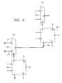
- FIG. 7 depicts a cluster with an output register connected to the multiplexer.
- FIG. 8A depicts a register with enable configuration for a multiplexer with register.
- FIG. 8B depicts a register with reset configuration for a multiplexer with register.
- FIG. 9 depicts a multiplexer with additional input selection logic.
- FIG. 10 depicts a multiplexer with input selection logic configured as a feedback circuit.
- FIG. 11 depicts a multiplexer configured to provide an alternate route for a carry-out signal.
- FIG. 12 depicts a cluster with additional elements to implement a registered path from the carry out output to the carry-in input of the ALU.
- FIG. 13 depicts a cluster with an inverter connected to the multiplexer output.
- FIG. 14 is a flowchart of a method for assigning application logic components to processing elements.
- FIG. 15 depicts a circuit for generating and selecting a multiplexer control signal.
- FIG. 16 depicts a circuit for selectively inverting a multiplexer control signal.
- FIG. 17 depicts an extension to the circuit of FIG. 15 , which allows a value to be diverted to control extended circuitry.
- FIG. 18 depicts a circuit implementing sign extensions, which can be mapped onto the cluster of FIG. 3 .
- FIG. 19 depicts a collection of ALUs and multiplexers arranged into clusters.
- FIG. 20 depicts a reconfigurable array including two general purpose routing networks for control signals.
- the array discussed in this embodiment is constructed using ALUs and multiplexers as first and second types of processing elements.
- ALUs ALUs
- multiplexers multiplexers
- the array can be constructed using lookup table based elements, product-term based elements, hardwired elements such as dedicated multiplier blocks, floating-point processors, integer processors, or other elements capable of implementing a combinatorial logic function.
- a cluster includes a collection of processing elements, including at least one processing element of a first type and one processing element of a second type.
- the first type and second type processing elements within a cluster are connected to each other with direct intra-cluster connections, which may be wires, busses, or other forms of electrical connections.
- the intra-cluster connections are not part of any general-purpose routing network present on the array. There may, however, be a connection with the general-purpose routing network at a cluster boundary.
- a cluster is defined as a set of processing elements that are connected directly or indirectly by the complete set of connections that directly connect non-identical elements.
- any of the processing elements within a cluster can be reached from any other processing element in the cluster by following the intra-cluster connections between first type and second type processing elements or vice versa, without regard to the direction that signals actually travel over the intra-cluster connections.
- any path of intra-cluster connections connecting non-identical types of processing elements defines a cluster.
- the path ALU-MUX-ALU-MUX describes a cluster, but the path ALU-MUX-MUX does not, since there is a connection between two processing elements of the same type in the path.
- a path A-B-C-A describes a cluster, but A-B-B-C-A does not, because of the B-B connection.
- a cluster may also include connections between processing elements of the same type, as long as there exists a path between each pair of processing elements in the cluster as described above.
- FIG. 19 depicts an example of clusters.
- the processing elements are designated by the “ALU” and “MUX” elements, and the connections are designated by the lines connecting elements.
- the first cluster 1910 includes all of the processing elements 1910 ( a )-( f ), on the left side of the dashed line.
- the second cluster 1920 includes all of the processing elements 1920 ( a )-( g ), on the right side of the dashed line.
- Each processing element 1910 ( a )-( f ) can be reached from each other processing element 1910 ( a )-( f ) by following a series of ALU-MUX or MUX-ALU connections.
- each processing element 1920 ( a )-( g ) can be reached from each other processing element 1920 ( a )-( g ) by following a series of ALU-MUX or MUX-ALU connections.
- No processing element 1910 ( a )-( g ) can be reached from a processing element 1920 ( a )-( g ) by following ALU-MUX or MUX-ALU connections.
- At least one ALU-ALU or MUX-MUX connection must be followed. Therefore, the processing elements 1910 ( a )-( f ) are not members of the second cluster 1920 , and the processing elements 1920 ( a )-( g ) are not members of the first cluster 1910 .
- An “ALU” is a processing element which is configurable to implement various mathematic and logic functions, depending on an instruction value.
- the ALU receives one or more data inputs, and applies the function selected by the instruction value to the data inputs, generating a data output.
- the ALU may also receive a carry-in value from another processing element, and depending on the data and instruction values received, may provide a carry-out output value to another processing element.
- a “multiplexer” is a processing element which receives two or more data input values and provides one of the data input values to a data output, based on a select input value.
- an ALU 100 for use in a reconfigurable array includes a first data input 110 , a second data input 120 , and an instruction input 130 .
- the data and instruction inputs receive input values from other elements within the array, or from elements connected to the array.
- the data and instruction inputs receive input values of a first bit width.
- the ALU 100 also includes a carry-in input 140 (“C in ”), which is of a second bit width. This input is used to receive a carry input from another ALU 100 in the array.
- C in carry-in input 140
- the ALU 100 also includes a carry-out output 150 (“C out ”), which is also of the second bit width.
- the carry-out output 150 provides a carry output to other elements within the array or to other elements connected to the array.
- the carry-in input 140 and the carry-out output 150 can provide values other than carry values, as desired by the designer.
- the ALU 100 also includes a data output 160 , of the first bit width.
- the data output 160 provides the result of the mathematic or logical function performed by the ALU to other elements within the array, or to other elements connected to the array.
- the ALU 100 also includes a select signal output 170 , of the second bit width.
- the select signal output 170 provides a select signal to other elements within the array or to other elements connected to the array.
- the select signal may be any of a wide variety of signals useful to control the functioning of another element within the array or connected to the array.
- the select signal may be one or more of the following data-dependent signals:
- the ALU 100 is adapted to store an internal instruction independent of the instruction input 130 . This allows the instruction input 130 to be used as a dedicated select signal input, by providing part or all of the instruction input 130 directly to the select signal output 170 , while using the stored instruction value to control the ALU 100 .
- the select signal output 170 may also include additional circuitry to select various signals routed from the ALU 100 , as discussed in further detail below.
- a multiplexer 200 for use in the reconfigurable array includes a first input 210 and a second input 220 , both of the first bit width.
- the inputs 210 , 220 receive input values from other elements within the array, or from elements connected to the array.
- the multiplexer 200 also includes an output 230 , of the first bit width.
- the output 230 provides the results of the input selection performed by the multiplexer 200 to other elements within the array, or to elements connected to the array.
- the multiplexer 200 also includes a select input 240 .
- the select input 240 receives a selection value that indicates which of the inputs 210 , 220 is to be directed to the output 230 .
- the select input 240 is of the second bit width. In this embodiment, a selection value of “1” results in the first input 210 being directed to the output 230 , and a selection value of “0” results in the second input 220 being directed to the output 230 .
- the first bit width is word-wide, being four bits wide and the second bit width is one bit wide.
- the first bit width and second bit width can be any size, as desired by the particular implementation contemplated by the designer.
- the inputs and outputs of the first bit width are preferably connected to a first general-purpose routing network, useful to route signals across the various elements of the array.
- the inputs and outputs of the second bit width are preferably connected either directly to another processing element or else connected to a second general purpose routing network adapted to carry signals of the second bit width. In either case, the second bit width signals bypass the first general-purpose routing network.
- the second bit width signals are routed across the first general-purpose routing network, along with the first bit width signals.
- the various inputs and outputs can be connected using various wires, busses, or other electrically conductive devices or current paths.
- a cluster 300 includes an ALU 100 and a multiplexer 200 .
- the select output 170 of the ALU 100 provides a select signal to the select input 240 of the multiplexer 200 .
- the multiplexer 200 can be controlled by either a data-dependent or an instruction-dependent signal. In terms of their usefulness in an application, these two cases are broadly equivalent to conditional and unconditional branching in a processor.
- Additional multiplexers can be added to the cluster 300 , as desired by the designer. These additional multiplexers may be controlled by the same select signal as controls the multiplexer 200 , or they may be controlled by different select signals.
- the cluster 300 may also be extended by the addition of other elements, such as additional ALUs, registers, gates, etc., attached to the various inputs and outputs of the elements within the cluster 300 .
- a cluster 300 may also be connected to other clusters, to implement more complex circuits. Various examples of such extensions are discussed in more detail below.
- the cluster 300 can be used alone or in combination with other clusters 300 to implement a wide variety of circuits, examples of which are provided in FIGS. 4-6 .
- a cluster 300 is used to implement a data selection circuit.
- the first input 110 carries a signed 4-bit value A, to be converted to an 8-bit value.
- the multiplexer inputs 210 , 220 carry the values “1111” and “0000” respectively.
- the ALU 100 evaluates the function A ⁇ 0, to generate the proper sign signal in the select output 170 and to propagate the input value A to the ALU output 160 .
- the sign output signal is used to switch the multiplexer 200 to select either “1111” or “0000”.
- the 8-bit result is constructed from the value on the ALU output 160 , and the value on the multiplexer output 230 .
- the cluster 300 can also be configured to propagate a second bit width signal generated by the ALU 100 onto the first bit width general-purpose routing network.
- the second bit width select signal generated on the select output 170 of the ALU 100 is routed to the select input 240 of the multiplexer 200 .
- the first input 210 is provided with a value “0001”, which is a first bit width representation of the second bit width value “1”.
- the second input 220 is provided with a value “0000”, which is a first bit width representation of the second bit width value “0”.
- the select signal is “1”
- the multiplexer 200 causes the first input value 210 of “0001” to be routed to the output 230 , and from there onwards to the general-purpose routing network.
- the multiplexer 200 causes the second input value 220 of “0000” to be routed to the output 230 , and from there onwards to the first general-purpose routing network.
- the select signals such as sign, overflow, carry out, etc, are efficiently converted from the second bit width to the first bit width and placed on the first general-purpose routing network, where they can be sent onwards to other processing elements. This provides an alternate path for these signals, in addition to the dedicated connections and second general purpose routing network discussed above.
- a first cluster 510 and a second cluster 550 are used to implement a condition processing circuit.
- the condition processing circuit performs a logical operation on one or more conditions provided as select output values of the ALUs.
- the first cluster 510 includes a first ALU 520 which generates a first condition (e.g. “sign” of the output value F 1 ), and passes the first condition to a first multiplexer 530 .
- the first multiplexer 530 receives a constant value of “0001” on the first input 533 , and a constant value of “0000” on the second input 535 . If the first condition is “1”, then the first multiplexer 530 selects the first input 533 to provide to the output 537 , otherwise the first multiplexer 530 selects the second input 535 to provide to the output 537 .
- the second cluster 550 includes a second ALU 560 which generates a second condition (e.g. “sign” of the output value F 2 ), and passes the second condition to a second multiplexer 570 .
- the second multiplexer receives the value from the output 537 on the first input 573 , and a constant value of “0000” on the second input 575 . If the second condition is “1”, then the second multiplexer 570 selects the first input 573 to provide to the output 577 , otherwise the second multiplexer 570 selects the second input 575 to provide to the output 577 .
- condition processing circuit of FIG. 5 produces as an output the logical AND of the two conditions S 1 and S 2 .
- Other logic functions can be similarly generated.
- the first cluster 510 and the second cluster 550 are configured to implement a datapath control circuit.
- the first ALU 520 generates a select signal as discussed above and sends the select signal to the first multiplexer 530 .
- the first multiplexer 530 receives a data input signal corresponding to an addition (“ADD”) instruction value on the first input 533 , and a data input signal corresponding to a subtraction (“SUB”) instruction value on the second input 535 . These data inputs will typically be multi-bit signals, as discussed above. Based on the value of the select signal, the first multiplexer 530 routes either the ADD or the SUB instruction value to the instruction input 562 of the second ALU 560 .
- the output of the second ALU 560 is therefore either A 2 +B 2 or A 2 ⁇ B 2 , depending on the condition generated by the first ALU 520 .
- a datapath within the array containing the first and second clusters 510 , 550 is controlled by altering the function performed by the second ALU 560 .
- Any desired datapath control function can be implemented by varying the data and instruction inputs to the first ALU 520 and first multiplexer 530 .
- an output register can be added to the cluster 300 to create additional useful circuits. These circuits are useful for performing data formatting for serial-to-parallel and parallel-to-serial conversion of data.
- the circuit of FIG. 7 includes the ALU 100 and multiplexer 200 as discussed above. Additionally, there is a register 700 attached to the output 230 of the multiplexer 200 . The register 700 stores a value loaded in from the output 230 of the multiplexer 200 .
- a switch 710 is adapted to route either the multiplexer output 230 or the register output 720 onwards to other elements. The switch 710 is set as part of the configuration of the application onto the array. In an alternate embodiment, there is a second register connected to the output 160 of the ALU 100 , either with or without a corresponding switch.
- FIGS. 8A and 8B show implementations of useful register circuits that can be implemented using the cluster 300 .
- FIG. 8A is an implementation of a “register with enable” circuit
- FIG. 8B is an implementation of a “register with reset” circuit.
- the “register with enable” circuit of FIG. 8A provides a register where the register contents only update (with the “input” value) when “enable” is active on a clock edge, otherwise the stored value is recycled and the output is unchanged.
- the “register with reset” circuit of FIG. 8B provides the value “input” to the register as long as the reset signal is inactive. When the reset signal goes active, then a zero value is loaded into the register on the next clock edge.
- Both of these register options are commonly used in applications, and thus these circuits are useful in implementing applications on a reconfigurable array and can be easily constructed with the “multiplexer and register” arrangement of FIG. 7 .
- multiplexers involve having a constant value on one or both of the inputs to the multiplexer, e.g.:
- the input selection logic is a trade-off which increases the size of the multiplexers but reduces the number of signals that are propagated through the routing networks.
- the multiplexer 200 as shown in FIG. 9 , has a first input multiplexer 910 and a second input multiplexer 920 attached to the first input 210 and second input 220 respectively.
- the first input multiplexer 910 is adapted to provide either a first input value 913 or a first constant value 917 (here the value “0001”) to the first input 210 .
- the second input multiplexer 920 is adapted to provide either a second input value 923 or a second constant value 927 (here the value “0000”) to the second input 220 .
- the input multiplexers 910 , 920 are not intended to be controlled dynamically by the application.
- the control signals for the input multiplexers 910 , 920 are set when the application is loaded into the array, and do not vary thereafter. In an alternate embodiment where a higher level of control over the array is desired, the input multiplexers 910 , 920 are dynamically controllable.
- the input multiplexers 910 , 920 may be extended to include other signals, either constant or variable.
- the second input multiplexer 920 is extended by adding the feedback signal as an input to the second input multiplexer 920 .
- the second input multiplexer 920 can be configured to form a feedback path 1010 to the second input 220 , in order to implement the “register with enable” circuit of FIG. 8A .
- the first input multiplexer 910 is extended by providing the carry out signal from the carry out output 150 of the ALU 100 to the first input multiplexer 910 .
- the carry out signal is padded with leading zeros.
- a carry out signal of “1” is padded to “0001” when provided to the first input multiplexer 910 .
- the first input multiplexer 910 provides the carry out output 150 to the multiplexer 200 , via the first input 210 .
- This provides another route to provide the carry out signal to the first general-purpose routing network.
- the carry out signal is already available to the multiplexer 200 via the select input 170 , and thus can be propagated to the first general-purpose routing network that way, this modification makes it possible to create a carry register with enable (or reset by modifying the circuit of FIG. 8B ) in one multiplexer 200 and one register 700 (not taking into consideration any input multiplexers that may be present).
- a resettable carry output register is useful in serial arithmetic applications.
- FIG. 12 a further useful modification of the circuit of FIG. 11 is to allow one of the bits of the register 700 or multiplexer 200 output to be used as a dedicated carry input to the ALU.
- a bit from the 4-bit output 230 of the multiplexer 200 is routed to an input multiplexer 1210 connected to the carry-in input 140 of the ALU 100 . This creates a registered path from the carry out output 150 to the carry-in input 140 .
- Such a path is useful when creating serialized arithmetic circuits, especially when combined with the ability to reset the register 700 as discussed above.
- FIGS. 10-12 show the feedback path to the second input multiplexer 920 being connected to the output of the switch 710 .
- the feedback path could be connected to the output of the register 700 , before the switch 710 .
- making the connection after the switch 710 makes it possible to choose the unregistered path, and thereby construct an asynchronous latch.
- FIG. 13 yet another extension of the basic circuit of the cluster 300 is shown.
- an inverter 1310 to the output 230 of the multiplexer 200 , the range of functions generateable by the multiplexer 200 is increased. It is possible for the multiplexer 200 to provide NAND and NOR gates:
- the latter option connects the A signal to a data input 210 , 220 of the multiplexer 200 rather than to the select input 240 . This may be preferable if there are different routing delays to the data inputs 210 , 220 and the select input 240 .
- circuits discussed above are merely examples of the wide variety of circuits that can be implemented using the clusters 300 of an embodiment of the invention.
- Heterogeneous arrays including the clusters 300 discussed above are able to implement many circuits smaller and faster than homogeneous arrays purely of ALUs.
- Multiplexers are significantly smaller and faster than ALUs, and therefore circuits that can make use of multiplexers are smaller and faster than equivalent circuits made up purely of ALUs. Operations such as condition processing, data formatting and instruction selection are all implemented more efficiently with a mix of multiplexers and ALUs than they would be with ALUs alone.
- a first general-purpose routing network is provided for routing of data and instructions amongst the elements of the array, and additional interconnect provides a multiplexer control network for routing of select signals between ALUs and multiplexers.
- This multiplexer control network may be a simple direct connection between an ALU and one or more associated multiplexers within a cluster, or it may be a more complex control network adapted to connect an ALU select output to multiplexers within the same cluster, within other clusters, or both.
- This control network may take the form of a second general-purpose routing network, separate from the first and optimized for carrying multiplexer control signals rather than data and instructions.
- the heterogeneous array of an embodiment significantly reduces problems in determining the proper mixture of element types.
- Multiplexers are useful to implement a wide variety of application logic components, such as bit-level logic, data reformatting, and dynamic instruction selection. Therefore, most applications that a designer might wish to implement on the heterogeneous array will be able to use multiplexers to some degree.
- Multiplexers are not the only way to implement the functions for which they are useful.
- An ALU can be used to implement any functions that a multiplexer can do.
- the multiplexer is just usually a more efficient implementation. Therefore, an application can be divided into three types of logic components:
- any or all of these categories may have subcategories, indicating a relative level of preference within the category. These subcategories are used to fine-tune the allocation of logic components to processing elements, depending on the specific mix of processing elements provided in the array and the various amounts of logic components in each category.
- the existence of the third category means that it is not necessary to find the “perfect” ALU-to-multiplexer ratio that guarantees there are always enough multiplexers (or ALUs) for all applications. Instead, when deciding how to allocate logic components amongst the processing elements, the method of FIG. 14 is used.
- the logic components which are preferably implemented in the first processing element type are identified and allocated to processing elements of the first type. If there are sub-categories indicative of a relative preference within the category, then the components with the strongest preference are allocated first.
- the components which are preferably implemented in the second processing element type are identified and allocated to processing elements of the second type. If there are sub-categories indicative of a relative preference within the category, then the components with the strongest preference are allocated first.
- the remaining logic components are allocated between the remaining processing elements of the first and second types according to a heuristic. For example, the remaining logic components are allocated to the second type elements until there are no more second type elements remaining, and then allocated to the first type elements. Alternatively, the remaining elements are split by their sub-category, with those logic components having a relative preference for the second type going to the second type and those logic components having a relative preference for the first type going to the first type.
- the select signal output 170 of the ALU 100 can comprise any of a variety of different signals.
- FIG. 15 an example of a selection circuit 1500 for generating and selecting a control signal used to control the multiplexer 200 will now be discussed in more detail.
- the selection circuit 1500 includes a plurality of status inputs 1510 adapted to receive status bits from the ALU 100 , together referred to as an ALU status word (ASW).
- Each of the status inputs 1510 carries a bit indicating a particular status signal, such as Sign, Overflow, Carry-Out, or a bit from the instruction input 130 , or any other data useful for controlling the multiplexer 200 .
- the selection circuit 1500 also includes a plurality of mask inputs 1520 , together referred to as a mask word.
- the mask inputs 1520 are adapted to receive mask values, which are used to mask out one or more of the status bits of the ALU status word.
- the mask inputs 1520 may receive their mask values from a wide variety of sources.
- the mask inputs 1520 may be connected to the first general-purpose routing network, and thereby receive mask values dynamically from other processing elements in the array.
- the mask inputs 1520 may be connected to local memory cells which store mask values, including mask values loaded into the array when it is configured for a particular application.
- the status inputs 1510 and the mask inputs 1520 are connected to a plurality of AND gates 1530 , which are adapted to perform a bitwise AND on the inputs 1510 , 1520 .
- the AND gates 1530 are all connected to an OR gate 1540 , which combines the AND'ed values together to form a single bit output provided to the select input 240 of the multiplexer 200 , to control the multiplexer 200 .
- Setting the mask word to all 0's means that the multiplexer control signal sent to the select input 240 will be zero, i.e. the multiplexer 200 will be fixed to always supply the value on the second input 220 to the output 230 . If one of the bits of the ASW is a constant 1, then selecting this bit with the mask word means that the control signal will be 1, i.e. the multiplexer 200 will be fixed to always supply the value on the first input 210 to the output 230 . In combination with the all 0's case, this provides the ability to set the multiplexer control signal to either constant 0 or constant 1.
- the selection circuit 1500 is extended by placing an XOR gate 1610 on the output of the OR gate 1540 , so that the output of the OR gate can be inverted.
- the other input to the XOR gate 1610 is tied to a data source 1620 which is loaded with a value during configuration of the array. If the value is “1”, then the XOR gate 1610 operates as an inverter, inverting the output value from the OR gate 1540 . If the value is “0”, then the XOR gate 1610 propagates the output of the OR gate 1540 . Thus, the XOR gate 1610 functions as an “inverter with enable.” This behavior is shown in Table 2:
- the mask word is set to all 0's, and the data source value is set to 0. If a constant 1 is desired to be sent to the select input 240 , the mask word is set to all 0's, and the data source value is set to 1. This alternative also allows the output of the OR gate 1540 to be inverted for all values of the mask word.
- the polarity of control to the multiplexer 200 can be varied.
- the second input 220 would be selected instead of the first input 210 by a “1” output from the OR gate 1540
- the first input 210 would be selected instead of the second input 220 by a “0” output from the OR gate 1540 .
- An example of this is where a feedback path from a register output only connects to one of the inputs 210 , 220 , or where a dedicated constant input is only available on one of the inputs 210 , 220 .
- the ASW can include, for example, bits representing any or all of the following values:
- the ALU instruction value can be stored in a register within the ALU, in which case the instruction input 130 is available for use as a dedicated multiplexer control input. This means that the instruction input 130 can be used to cover both the “bits from an instruction input” and the “bits from a data input” in the above list. Consequently, a useful subset of this list includes: carry out, correct sign and 2 bits from the ALU instruction input 130 .
- the multiplexer control signal can be, for example, one of the following:
- bits of the instruction input 130 should be available in the ASW are the following examples:
- the LSB is the bit used to propagate carries across the routing network, as it means that carry values have the correct numeric value (1 if there is a carry, 0 if there is not). Being able to connect a carry via the instruction input 130 means that the multiplexer 200 can be controlled by carry from its local ALU 100 and also (indirectly) by carry from any other ALU 100 in the array.
- the MSB is selected for a similar reason—it is the sign bit in a word, so being able to choose it gives flexibility over the choice of sign data.
- Instruction LSB and Instruction bit n/2 i.e. bit 2 in a 4-bit Word, 3 in a 6-bit Word . . . )
- the LSB is selected for the same reasons as choice #1 above.
- An alternative useful subset for the ASW is a 5-bit word including the 4 bits of the instruction input 130 , plus the ALU carry output 150 . This subset has the following advantages:
- n-bit mask to choose which bits of the ALU status word are to be connected to the select input 240 implies that there are 2′′ possible combinations that may be used. In practice some combinations are much less common than others, and some are never used.
- the circuit 1500 discussed above can be extended to include efficient connections to various networks, (such as the second general-purpose routing network mentioned above) and can do so by making use of the uncommon parts of the ASW encoding scheme described above.
- the “All mask bits set” state can be used to select an alternative input to the multiplexer control path, as shown in FIG. 17 .
- the circuit 1500 as extended includes a 4-input AND gate 1710 , which draws its inputs from the mask inputs 1520 .
- the output of the 4-input AND gate 1710 is connected to the select input of a multiplexer 1720 .
- the multiplexer 1720 receives a first input 1730 from the high-fanout network, and a second input 1740 from the circuit 1500 .
- the multiplexer 1720 provides an output to the XOR gate 1610 , to convey a select signal to the select input 240 of the multiplexer 200 as discussed above.
- the multiplexer 1720 When the mask inputs 1520 are configured to all 1's (the final row of Table 3), this causes the output of the 4-input AND gate 1710 to go high (1), which causes the multiplexer 1720 to select the first input 1730 , from the high-fanout network, to provide the select signal to the multiplexer 200 , via the XOR gate 1610 .
- the multiplexer 200 is controlled by a signal routed across the high-fanout network.
- the output of the 4-input AND gate 1710 stays low (0), causing the multiplexer 1720 to select the second input 1740 , from the circuit 1500 , to provide the select signal to the multiplexer 200 , via the XOR gate 1610 .
- the multiplexer 200 is controlled by the ALU 100 , as discussed above.
- the ASW processing logic such as the circuit 1500 , optionally extended as discussed, is also a useful source of high-fanout control signals to be provided to the high-fanout control network.
- “Global” control signals are typically derived in a similar way to “local” control signals, they are just provided to a larger part of the array. Therefore, the output of the circuit 1500 is also routed to the high-fanout control network.
- the output may be routed directly to the high-fanout control network as shown in FIG. 17 , or alternatively the output can be routed first through the multiplexer 1720 , with the connection to the high-fanout network being made to the output of the multiplexer 1720 . This alternative connection allows the high-fanout output to be derived from the high-fanout input instead.
- Variants of this circuit are possible which decode multiple “uncommon” states from the ASW selection table (Table 3) and choose between multiple inputs from the high-fanout network. Alternatively these multiple uncommon states can be used to select a state to drive the high-fanout output.
- the high-fanout output can be connected to the high-fanout network.
- a useful way is to make the connection via a tri-state buffer, with the tri-state enable driven by part of the configuration state of the device (e.g. a dedicated configuration bit).
- This form of connection has the advantage that multiple sources are capable of driving the high fanout wire, but the timing is independent of which one is actually used. This makes the timing of the high fanout network easy for routing software to analyze.
- the above section describes the usefulness of high-fanout control signals, and an example of how they could be interfaced to the multiplexer control circuit 1500 .
- This section provides an example of a useful connection pattern for the high-fanout connection wires to use, to create a general purpose routing network.
- processing elements in a reconfigurable array are arranged in rows and columns on an X-Y grid, either a fully populated grid or a partially populated one (e.g. a checkerboard or chessboard arrangement).
- a fully populated grid or a partially populated one (e.g. a checkerboard or chessboard arrangement).
- those elements sharing a common multiplexer control signal can be arranged in:
- the array contains high fanout wires in both the horizontal and vertical directions.
- Each individual high fanout wire runs either horizontally or vertically (i.e. along a row or a column), and connects to all the ALUs 100 that it crosses.
- the wires may run along the whole row (column) or just part of it.
- the high fanout wires connect to the multiplexer control circuits 1500 as indicated above, with the following additional constraints:
- wires naturally run in horizontal and vertical directions, so it is easy to make row and column connections as described above. Furthermore, the ability to input from a horizontal wire and output to a vertical one (or vice versa) makes it possible to create 2-dimensional patches—a horizontal wire can be connected to several vertical wires that it crosses.
- a checkerboard arrangement such as shown in FIG. 20 , has the property that there are no ALUs in an even row but an odd column (or vice versa)—those sites are occupied by the spaces between ALUs, or more commonly by hardware to support the routing network.
- the connection pattern described above results in the creation of two independent control networks 2010 a and 2010 b —one linking the ALUs 2000 in odd numbered rows and columns, and the other linking the ALUs 2000 in even numbered rows and columns.
- the lines between ALUs 2000 depict the control network connections. Lines crossing within an ALU 2000 are connectable to each other to form a control network 2010 a , 2010 b .
- Lines crossing outside of the ALUs 2000 are not connectable to each other to form control networks 2010 a , 2010 b . This may be an acceptable situation, with the two networks used to distribute two separate control signals, Alternatively it may be found to be useful to provide connections between these two networks 2010 a , 2010 b . The points at which they cross will lie over the routing regions of the checkerboard, so it is easy to support this connection if required.
- the general-purpose routing networks 2010 a , 2010 b are separate from the first general-purpose routing network described above.
- a signal can only propagate from 2010 a , 2010 b to the first general-purpose routing network by controlling a multiplexer in the manner described in connection with FIG. 4B above.
- FPGA and RAA devices can support a wide range of wordlengths, limited only by the granularity of the processing elements that make up the array (i.e. if the array has 4-bit processing elements then it can directly handle wordlengths equal to 4n (positive integer n)).
- the efficiency penalty can be quite significant—e.g. changing from a 16-bit to a 32-bit implementation can double the amount of memory required for intermediate results and halve the throughput of the main datapath. However the possibility of occasional errors may be unacceptable.
- processors therefore have an overflow detection mechanism that identifies when the result of a calculation doesn't fit in the target wordlength, and can branch to another part of the program when an overflow happens. “Overflow” is therefore an important concept for processors.
- the situation is significantly different—the cost of extending the wordlength is significantly lower because of the finer-grain control of wordlength, and the cost of branching is significantly higher.
- the application normally fits in 16 bit words, but occasionally requires 18 bits.
- a processor would have to use 32 bit words to handle these cases, but an RAA with 4-bit processing elements could use a 20-bit datapath.
- the penalty for supporting the worst-case situation is therefore a 25% area increase, not a 100% increase.
- FPGA and RAA commonly implement branching by building datapaths for all possible paths through a program. They then use multiplexers to select the correct path for a particular data set. Having a 16-bit primary datapath with some sections repeated using 20 bits, plus multiplexing to choose between them can quickly result in a larger implementation than simply using a wider datapath throughout.
- processors are bad at fine-grain wordlength control but good at branching, while FPGA and RAA are better at wordlength control, and worse at branching.
- Overflow detection is a way of converting wordlength problems into branches, and is therefore appropriate for processors, but not for FPGA or RAA.
- wordlength control and branching in processors, FPGA and RAA described above also have an impact on how signs are computed and used.
- processors use branching as their main control mechanism, and they use comparisons to control branching. This is done either with a combined “compare and branch” instruction or with separate “compare and set flag” and “branch if flag set” instructions. There is therefore some similarity between comparison operations and the description of overflow handling above—they both have a “do an operation” stage followed by a “branch if some condition occurs”. (i.e. if there is an overflow, or if the comparison was true) This similarity is often made explicit, with the processor having a set of “condition flags” that indicate which of a set of interesting conditions have occurred (such as arithmetic overflow, calculation produced a negative result (i.e. “sign”), most recent carry out value), and a generic branch instruction that jumps if one or more of a specified subset of the flags are set.
- condition flags that indicate which of a set of interesting conditions have occurred (such as arithmetic overflow, calculation produced a negative result (i.e. “sign
- Sign extension normally takes place as data is loaded into the processor from memory. If the data is stored in a format that is more compact than the format into which it is being loaded, then sign extension is an option on the load operation, replicating the MSB of the stored representation into the extra bits of the in-processor version.
- Branching is an inefficient operation in an FPGA. Comparison operations in an FPGA are more likely to be used as control inputs to multiplexers, or blocks of logic to combine multiple conditions. Computation of sign is a straightforward operation, as the 1-bit nature of the routing network makes it easy to directly implement the expressions for the correct sign given below.
- Sign extension in an FPGA can be a routing operation—the 1-bit nature of FPGA routing allows a sign bit to be easily connected to multiple destinations. However, there is often no need to extend the inputs to an arithmetic operation as it is easy to implement operators with n-bit inputs and n+1-bit outputs.
- RAA is an intermediate case between processors and FPGAs—generic branching is still inefficient (although some limited forms can be implemented by multiplexing of instructions) but the routing network is word-based rather than bit-based, so a direct implementation of the expressions for sign and overflow is more complex, requiring shifts to adjust the positions of bits within the words. It is therefore worth considering adding extra logic to the RAA ALU to directly generate Sign and/or Overflow. For example, Sign is useful, and requires just 1 XOR gate to implement it.
- Sign extension cannot be a simple routing option, due to the need to realign bits within words.
- sign extension of arithmetic outputs can also be used with RAA, and benefits directly from the availability of a sign signal.
- the circuit of FIG. 18 with the sign output 1810 of an addition (or subtraction) operation 1820 controlling a multiplexer 1830 —maps directly onto the ALU 100 and multiplexer 200 of the cluster 300 shown in FIG. 3 . It is identical to the circuit structure used for data selection following a signed comparison illustrated in FIG. 4A .
- the circuit receives as inputs two numbers to be added or subtracted, and generates as output the result of the operation and an additional number of bits that pad the output to the desired length, by extending the sign value.
- the multiplexer 1830 selects the first input value of all 1's to pad the result. If the sign output 1810 carries a value of “0”, indicating a positive number, then the multiplexer 1830 selects the second input value of all 0's to pad the result.
- dedicated sign logic is of little benefit to an FPGA as it can directly implement the required logic. It is of much greater benefit to processors (as a control flag for a branch) and to RAA as a control signal for multiplexers 200 where it can be used for both conditional control and sign extension.
- Input extension is achieved by repeating the MSB.
- ⁇ n ⁇ 1 A n ⁇ 1 ⁇ B n ⁇ 1 ⁇ C n ⁇ 2
- C n ⁇ 1 if( A n ⁇ 1 ⁇ B n ⁇ 1 )then( C n ⁇ 2 )else( A n ⁇ 1 )
- ⁇ n A n ⁇ B n ⁇ C n ⁇ 1
- a n A n ⁇ 1
- B n B n ⁇ 1
- n A n ⁇ 1 ⁇ B n ⁇ 1 ⁇ C n ⁇ 1
- the overflow signal can be generated with a single XOR gate combining carry in and carry out of the last stage of the n-bit calculation.
- N The correct sign, (often referred to as the negative flag, N) is equal to the extra output bit:
Abstract
Description
-
- High-speed processing elements prefer a high-speed interconnect;
- It is beneficial to route data in the same width as the data is processed by the processing elements.
-
- The number of possible connections grows as the square of the number of processing elements. The “cost per element” of an interconnect that guarantees no interference between connections therefore increases linearly with the number of processing elements.
- This may be affordable for small arrays, but is not for large ones.
- Propagation delay will tend to increase with the size of the array.
-
- If the applications written for use on the reconfigurable device are written such that the application can be implemented on a device having only nearest-neighbor connectivity, then the interconnect can be greatly simplified. If such simplification is not possible then a general-purpose routing network (as described above) is normally used as the basis of the interconnect, the terminals of the network being the terminals of the processing elements.
-
- FPGAs with both lookup table based elements and dedicated multiplier blocks;
- FPGAs with both lookup table based elements and product-term based logic; or
- Processor arrays containing both integer and floating-point processors.
-
- Dedicated wiring may be added to support common connection patterns, e.g. the “Carry wires” in many FPGAs.
- There may be dedicated nearest-neighbor connections in addition to a general purpose routing network.
-
- Are the A and B inputs equal?
- Is input A greater than input B?
- Is bit 3 of an input set to 1?
-
- Cout: The carry out from an ALU operation,
- Sign: The correct sign of an ALU operation (even in the event of an arithmetic overflow),
- Overflow: A signal indicating that there has been an arithmetic overflow.
| TABLE 1 | |||||
| S1 | Z1 = X2 | S2 | Output | ||
| 0 | 0000 | 0 | 0000 | ||
| 0 | 0000 | 1 | X2 = 0000 | ||
| 1 | 0001 | 0 | 0000 | ||
| 1 | 0001 | 1 | X2 = 0001 | ||
-
- Implementing an AND, OR or NOT gate,
- Propagating a carry out value to the first general purpose routing network, or
- Implementing a resettable register.
-
- NAND(A, B)=NOT (A?B:0)
- NOR(A, B)=NOT (A?1:B).
-
- NOT A=A?0:1—this form doesn't use an inverter
- NOT A=NOT(1?A:0)—this form uses an inverter.
-
- A & (NOT B)=B?0:A—this form does not use an inverter
-
- 1. That logic which is preferably implemented in ALUs,
- 2. That logic which is preferably implemented in multiplexers,
- 3. That logic for which there is a choice of implementation.
| TABLE 2 | |||
| data source | XOR | ||
| value | OR | Result | |
| 0 | 0 | 0 | |
| 0 | 1 | 1 | |
| 1 | 0 | 1 | |
| 1 | 1 | 0 | |
-
- ALU carry in,
- ALU carry out,
- ALU “overflow” (using the 2s complement definition of overflow),
- ALU “correct sign” (again, following the 2s complement definition),
- One or more bits taken directly from an
ALU data input - One or more bits taken directly from the
ALU instruction input 130
-
- The result of an unsigned comparison (less than, greater than), via carry out,
- The result of a signed comparison (less than, greater than), via the sign signal,
- The sign of a signed arithmetic operation, to be used for sign extension (again via sign signal),
- An overflow from an unsigned arithmetic operation (again via carry out),
- The result of an equality test (for ALU designs that report equality test results via carry out), or
- A bit derived from the
instruction input 130, with a choice of 2 instruction bits. (Also covers the “bits from a data input” option).
-
-
Extract bit 0 and n/2 - Rotate 1 place left
-
Extract bit 0 and n/2 (equivalent to bits n−1 and n/2−1) - Rotate 1 place left
-
Extract bit 0 and n/2 (equivalent to bits n−2 and n/2−2) - Rotate 1 place left
- etc.
gives an efficient, regular method to extract all n bits with n/2 rotates. For this to work the bits used to have to be spaced evenly within the instruction word, and sincebit 0 is useful for other reasons the other bit will be half a word up frombit 0.
-
| TABLE 3 | ||||
| Instr— | Instr— | |||
| Carry | Sign | LSB | MSB | |
| 0 | 0 | 0 | 0 | |
| 0 | 0 | 0 | 1 | |
| 0 | 0 | 1 | 0 | |
| 0 | 0 | 1 | 1 | |
| 0 | 1 | 0 | 0 | |
| 0 | 1 | 0 | 1 | |
| 0 | 1 | 1 | 0 | |
| 0 | 1 | 1 | 1 | Sign OR |
| 1 | 0 | 0 | 0 | |
| 1 | 0 | 0 | 1 | |
| 1 | 0 | 1 | 0 | |
| 1 | 0 | 1 | 1 | Carry OR |
| Instr_MSB | ||||
| 1 | 1 | 0 | 0 | |
| 1 | 1 | 0 | 1 | Carry OR |
| 1 | 1 | 1 | 0 | Carry OR |
| 1 | 1 | 1 | 1 | Carry OR Sign OR Instr_LSB OR |
| Instr_MSB | ||||
-
- “Global Reset,”
- “Global enable,” or
- Pipeline stall/enable.
-
- Rows, or
- Columns, or
- Approximately rectangular patches.
- (based on the assumption that the high-fanout control signal is being used to control a datapath that has a bitslice (or sub-word-slice) style layout).
-
- If there is more than one
multiplexer 200 perALU 100, then eachcircuit 1500 has its input from and output to the high-fanout wires connected to orthogonal wires (i.e. input from vertical, output to horizontal or vice versa). - If there is only 1
multiplexer 200 perALU 100 then thecircuit 1500 should be capable of connecting the inputs and outputs from/to the high-fanout network to both horizontal and vertical high-fanout wires.
- If there is more than one
-
- always run with a wordlength large enough to handle the rare cases, and accept the efficiency penalty to do this, or
- run with the smaller wordlength, and accept that the results may occasionally be wrong.
-
- in normal circumstances run with the smaller wordlength, but detect the situations where this gives the wrong answer so that remedial action can be taken if required. (e.g. rerun all or part of the calculation with a wider wordlength).
-
- Comparison:
- A>B can be implemented by subtracting A from B and checking the sign of the result (only the sign of the result is important, not the full value). Similar methods work for other comparisons (<, <=, >=).
- Sign Extension:
- When increasing the wordlength of a 2s complement signed number, the sign bit needs to be copied into all the added bits. This is normally a simple operation once the sign bit is known.
-
- −2decimal=NOT(010binary)+1binary=101binary+1binary=110binary.
- Unsigned comparison will always be correctly expressed by the carry out from the most significant bit of the calculation.
- Signed comparison by subtraction and testing the carry out from the MSB will give the wrong result in the event of an arithmetic overflow. This can be fixed with a combination of “Carry out” and “Overflow” signals, or by directly generating the sign signal.
- Unsigned “sign extension” is trivial—all the added bits are 0.
- Signed sign extension is as described above—the sign is copied into all the added bits.
Σi =A i ^B i ^C i−1
C i=if(A i ^B i)then(C i−1)else(A i)
Σn−1 =A n−1 ^B n−1 ^C n−2
C n−1=if(A n−1 ^B n−1)then(C n−2)else(A n−1)
Σn =A n ^B n ^C n−1
An=0
Bn=0
Σn=Cn−1
Σn−1 =A n−1 ^B n−1 ^C n−2
C n−1=if(A n−1 ^B n−1)then(C n−2)else(A n−1)
Σn =A n^Bn ^C n−1
An=An−1
Bn=Bn−1
Σn =A n−1 ^B n−1 ^C n−1
Claims (89)
Priority Applications (8)
| Application Number | Priority Date | Filing Date | Title |
|---|---|---|---|
| US10/188,388 US7471643B2 (en) | 2002-07-01 | 2002-07-01 | Loosely-biased heterogeneous reconfigurable arrays |
| EP03737986A EP1535394B1 (en) | 2002-07-01 | 2003-06-02 | Loosely-biased heterogeneous reconfigurable arrays |
| PCT/EP2003/005783 WO2004003778A2 (en) | 2002-07-01 | 2003-06-02 | Loosely-biased heterogeneous reconfigurable arrays |
| AT03737986T ATE418814T1 (en) | 2002-07-01 | 2003-06-02 | LOOSE POLARIZED, HETEROGENEOUS, RECONFIGURABLE GATE FIELD |
| AU2003245906A AU2003245906A1 (en) | 2002-07-01 | 2003-06-02 | Loosely-biased heterogeneous reconfigurable arrays |
| JP2004516568A JP4261478B2 (en) | 2002-07-01 | 2003-06-02 | Heterogeneous reconfigurable array |
| DE60325488T DE60325488D1 (en) | 2002-07-01 | 2003-06-02 | LOOSE POLARIZED HETEROGENIC RECONFIGURABLE GATTERFIELD |
| US11/130,613 US7461234B2 (en) | 2002-07-01 | 2005-05-16 | Loosely-biased heterogeneous reconfigurable arrays |
Applications Claiming Priority (1)
| Application Number | Priority Date | Filing Date | Title |
|---|---|---|---|
| US10/188,388 US7471643B2 (en) | 2002-07-01 | 2002-07-01 | Loosely-biased heterogeneous reconfigurable arrays |
Related Child Applications (1)
| Application Number | Title | Priority Date | Filing Date |
|---|---|---|---|
| US11/130,613 Continuation-In-Part US7461234B2 (en) | 2002-07-01 | 2005-05-16 | Loosely-biased heterogeneous reconfigurable arrays |
Publications (2)
| Publication Number | Publication Date |
|---|---|
| US20040001445A1 US20040001445A1 (en) | 2004-01-01 |
| US7471643B2 true US7471643B2 (en) | 2008-12-30 |
Family
ID=29780116
Family Applications (1)
| Application Number | Title | Priority Date | Filing Date |
|---|---|---|---|
| US10/188,388 Active 2026-10-13 US7471643B2 (en) | 2002-07-01 | 2002-07-01 | Loosely-biased heterogeneous reconfigurable arrays |
Country Status (7)
| Country | Link |
|---|---|
| US (1) | US7471643B2 (en) |
| EP (1) | EP1535394B1 (en) |
| JP (1) | JP4261478B2 (en) |
| AT (1) | ATE418814T1 (en) |
| AU (1) | AU2003245906A1 (en) |
| DE (1) | DE60325488D1 (en) |
| WO (1) | WO2004003778A2 (en) |
Cited By (8)
| Publication number | Priority date | Publication date | Assignee | Title |
|---|---|---|---|---|
| US20070192504A1 (en) * | 2006-02-16 | 2007-08-16 | Moore Charles H | Asynchronous computer communication |
| US20100228807A1 (en) * | 2009-03-03 | 2010-09-09 | Altera Corporation | Digital signal processing circuitry with redundancy and bidirectional data paths |
| US7904695B2 (en) | 2006-02-16 | 2011-03-08 | Vns Portfolio Llc | Asynchronous power saving computer |
| US7937557B2 (en) | 2004-03-16 | 2011-05-03 | Vns Portfolio Llc | System and method for intercommunication between computers in an array |
| US7966481B2 (en) | 2006-02-16 | 2011-06-21 | Vns Portfolio Llc | Computer system and method for executing port communications without interrupting the receiving computer |
| US8549055B2 (en) | 2009-03-03 | 2013-10-01 | Altera Corporation | Modular digital signal processing circuitry with optionally usable, dedicated connections between modules of the circuitry |
| US9779785B2 (en) | 2015-05-11 | 2017-10-03 | Wisconsin Alumni Research Foundation | Computer architecture using compute/storage tiles |
| US20170351633A1 (en) * | 2016-06-06 | 2017-12-07 | Hewlett Packard Enterprise Development Lp | Modifications to a stream processing topology during processing of a data stream |
Families Citing this family (17)
| Publication number | Priority date | Publication date | Assignee | Title |
|---|---|---|---|---|
| US7461234B2 (en) * | 2002-07-01 | 2008-12-02 | Panasonic Corporation | Loosely-biased heterogeneous reconfigurable arrays |
| US7471643B2 (en) | 2002-07-01 | 2008-12-30 | Panasonic Corporation | Loosely-biased heterogeneous reconfigurable arrays |
| US6944205B2 (en) * | 2002-07-09 | 2005-09-13 | Sandbridge Technologies, Inc. | Method of determining an acquisition indicator bit in a communication system |
| CN101044485A (en) * | 2003-06-18 | 2007-09-26 | 安布里克股份有限公司 | Integrated circuit development system |
| US20070186076A1 (en) * | 2003-06-18 | 2007-08-09 | Jones Anthony M | Data pipeline transport system |
| US7844668B2 (en) * | 2004-07-30 | 2010-11-30 | Microsoft Corporation | Suggesting a discussion group based on indexing of the posts within that discussion group |
| US20060181243A1 (en) * | 2005-02-11 | 2006-08-17 | Nortel Networks Limited | Use of location awareness to facilitate clinician-charger interaction in a healthcare environment |
| JP4527571B2 (en) * | 2005-03-14 | 2010-08-18 | 富士通株式会社 | Reconfigurable processing unit |
| CN100346335C (en) * | 2005-12-02 | 2007-10-31 | 浙江大学 | Reconfigureable computing unit using asynchronous communication mechanism |
| US7751368B2 (en) * | 2006-05-01 | 2010-07-06 | Intel Corporation | Providing CQI feedback to a transmitter station in a closed-loop MIMO system |
| CN101578767A (en) * | 2007-01-05 | 2009-11-11 | Nxp股份有限公司 | Circuit comprising a matrix of programmable logic cells |
| JP5015210B2 (en) * | 2009-08-14 | 2012-08-29 | 株式会社半導体理工学研究センター | High frequency signal generation circuit |
| JP2014016894A (en) * | 2012-07-10 | 2014-01-30 | Renesas Electronics Corp | Parallel arithmetic device, data processing system with parallel arithmetic device, and data processing program |
| US9628083B1 (en) * | 2015-10-01 | 2017-04-18 | Quicklogic Corporation | Local routing network with selective fast paths for programmable logic device |
| US10963265B2 (en) * | 2017-04-21 | 2021-03-30 | Micron Technology, Inc. | Apparatus and method to switch configurable logic units |
| CN117194311A (en) * | 2017-11-03 | 2023-12-08 | 相干逻辑公司 | Memory network processor |
| US11029958B1 (en) * | 2019-12-28 | 2021-06-08 | Intel Corporation | Apparatuses, methods, and systems for configurable operand size operations in an operation configurable spatial accelerator |
Citations (23)
| Publication number | Priority date | Publication date | Assignee | Title |
|---|---|---|---|---|
| US4811214A (en) | 1986-11-14 | 1989-03-07 | Princeton University | Multinode reconfigurable pipeline computer |
| US5038386A (en) | 1986-08-29 | 1991-08-06 | International Business Machines Corporation | Polymorphic mesh network image processing system |
| US5442577A (en) | 1994-03-08 | 1995-08-15 | Exponential Technology, Inc. | Sign-extension of immediate constants in an alu |
| US5715186A (en) | 1994-04-19 | 1998-02-03 | Sgs-Thomson Microelectronics S.A. | Digital processing device with minimum and maximum search instructions |
| US5742180A (en) | 1995-02-10 | 1998-04-21 | Massachusetts Institute Of Technology | Dynamically programmable gate array with multiple contexts |
| US5914953A (en) * | 1992-12-17 | 1999-06-22 | Tandem Computers, Inc. | Network message routing using routing table information and supplemental enable information for deadlock prevention |
| US6011795A (en) * | 1997-03-20 | 2000-01-04 | Washington University | Method and apparatus for fast hierarchical address lookup using controlled expansion of prefixes |
| US6052773A (en) | 1995-02-10 | 2000-04-18 | Massachusetts Institute Of Technology | DPGA-coupled microprocessors |
| WO2000069073A1 (en) | 1999-05-07 | 2000-11-16 | Morphics Technology Inc. | Heterogeneous programmable gate array |
| US6157967A (en) * | 1992-12-17 | 2000-12-05 | Tandem Computer Incorporated | Method of data communication flow control in a data processing system using busy/ready commands |
| US20020010902A1 (en) * | 2000-05-26 | 2002-01-24 | Zheng Chen | Field programmable gate array (FPGA) bit stream cormat |
| US20020138716A1 (en) | 2001-03-22 | 2002-09-26 | Quicksilver Technology, Inc. | Adaptive integrated circuitry with heterogeneous and reconfigurable matrices of diverse and adaptive computational units having fixed, application specific computational elements |
| US6469540B2 (en) | 2000-06-15 | 2002-10-22 | Nec Corporation | Reconfigurable device having programmable interconnect network suitable for implementing data paths |
| US6609189B1 (en) | 1998-03-12 | 2003-08-19 | Yale University | Cycle segmented prefix circuits |
| US20030200418A1 (en) * | 1996-04-11 | 2003-10-23 | Massachusetts Institute Of Technology | Intermediate-grain reconfigurable processing device |
| US20040001445A1 (en) | 2002-07-01 | 2004-01-01 | Elixent, Ltd | Loosely-biased heterogeneous reconfigurable arrays |
| US20040027995A1 (en) * | 1999-03-30 | 2004-02-12 | International Business Machines Corporation | Non-disruptive reconfiguration of a publish/subscribe system |
| US6781408B1 (en) | 2002-04-24 | 2004-08-24 | Altera Corporation | Programmable logic device with routing channels |
| WO2004075403A2 (en) | 2003-02-19 | 2004-09-02 | Koninklijke Philips Electronics N.V., | Electronic circuit with array of programmable logic cells |
| US6807172B1 (en) * | 1999-12-21 | 2004-10-19 | Cisco Technology, Inc. | Method and apparatus for learning and switching frames in a distributed network switch |
| US6907011B1 (en) * | 1999-03-30 | 2005-06-14 | International Business Machines Corporation | Quiescent reconfiguration of a routing network |
| US6965615B1 (en) * | 2000-09-18 | 2005-11-15 | Cisco Technology, Inc. | Packet striping across a parallel header processor |
| US7272691B2 (en) * | 2001-03-02 | 2007-09-18 | Mtekvision Co., Ltd. | Interconnect switch assembly with input and output ports switch coupling to processor or memory pair and to neighbor ports coupling to adjacent pairs switch assemblies |
Family Cites Families (1)
| Publication number | Priority date | Publication date | Assignee | Title |
|---|---|---|---|---|
| US678408A (en) * | 1897-03-06 | 1901-07-16 | Wilhelm Lengweiler | Ring-spinning machine. |
-
2002
- 2002-07-01 US US10/188,388 patent/US7471643B2/en active Active
-
2003
- 2003-06-02 AT AT03737986T patent/ATE418814T1/en not_active IP Right Cessation
- 2003-06-02 AU AU2003245906A patent/AU2003245906A1/en not_active Abandoned
- 2003-06-02 DE DE60325488T patent/DE60325488D1/en not_active Expired - Lifetime
- 2003-06-02 WO PCT/EP2003/005783 patent/WO2004003778A2/en active Application Filing
- 2003-06-02 EP EP03737986A patent/EP1535394B1/en not_active Expired - Lifetime
- 2003-06-02 JP JP2004516568A patent/JP4261478B2/en not_active Expired - Fee Related
Patent Citations (23)
| Publication number | Priority date | Publication date | Assignee | Title |
|---|---|---|---|---|
| US5038386A (en) | 1986-08-29 | 1991-08-06 | International Business Machines Corporation | Polymorphic mesh network image processing system |
| US4811214A (en) | 1986-11-14 | 1989-03-07 | Princeton University | Multinode reconfigurable pipeline computer |
| US5914953A (en) * | 1992-12-17 | 1999-06-22 | Tandem Computers, Inc. | Network message routing using routing table information and supplemental enable information for deadlock prevention |
| US6157967A (en) * | 1992-12-17 | 2000-12-05 | Tandem Computer Incorporated | Method of data communication flow control in a data processing system using busy/ready commands |
| US5442577A (en) | 1994-03-08 | 1995-08-15 | Exponential Technology, Inc. | Sign-extension of immediate constants in an alu |
| US5715186A (en) | 1994-04-19 | 1998-02-03 | Sgs-Thomson Microelectronics S.A. | Digital processing device with minimum and maximum search instructions |
| US6052773A (en) | 1995-02-10 | 2000-04-18 | Massachusetts Institute Of Technology | DPGA-coupled microprocessors |
| US5742180A (en) | 1995-02-10 | 1998-04-21 | Massachusetts Institute Of Technology | Dynamically programmable gate array with multiple contexts |
| US20030200418A1 (en) * | 1996-04-11 | 2003-10-23 | Massachusetts Institute Of Technology | Intermediate-grain reconfigurable processing device |
| US6011795A (en) * | 1997-03-20 | 2000-01-04 | Washington University | Method and apparatus for fast hierarchical address lookup using controlled expansion of prefixes |
| US6609189B1 (en) | 1998-03-12 | 2003-08-19 | Yale University | Cycle segmented prefix circuits |
| US20040027995A1 (en) * | 1999-03-30 | 2004-02-12 | International Business Machines Corporation | Non-disruptive reconfiguration of a publish/subscribe system |
| US6907011B1 (en) * | 1999-03-30 | 2005-06-14 | International Business Machines Corporation | Quiescent reconfiguration of a routing network |
| WO2000069073A1 (en) | 1999-05-07 | 2000-11-16 | Morphics Technology Inc. | Heterogeneous programmable gate array |
| US6807172B1 (en) * | 1999-12-21 | 2004-10-19 | Cisco Technology, Inc. | Method and apparatus for learning and switching frames in a distributed network switch |
| US20020010902A1 (en) * | 2000-05-26 | 2002-01-24 | Zheng Chen | Field programmable gate array (FPGA) bit stream cormat |
| US6469540B2 (en) | 2000-06-15 | 2002-10-22 | Nec Corporation | Reconfigurable device having programmable interconnect network suitable for implementing data paths |
| US6965615B1 (en) * | 2000-09-18 | 2005-11-15 | Cisco Technology, Inc. | Packet striping across a parallel header processor |
| US7272691B2 (en) * | 2001-03-02 | 2007-09-18 | Mtekvision Co., Ltd. | Interconnect switch assembly with input and output ports switch coupling to processor or memory pair and to neighbor ports coupling to adjacent pairs switch assemblies |
| US20020138716A1 (en) | 2001-03-22 | 2002-09-26 | Quicksilver Technology, Inc. | Adaptive integrated circuitry with heterogeneous and reconfigurable matrices of diverse and adaptive computational units having fixed, application specific computational elements |
| US6781408B1 (en) | 2002-04-24 | 2004-08-24 | Altera Corporation | Programmable logic device with routing channels |
| US20040001445A1 (en) | 2002-07-01 | 2004-01-01 | Elixent, Ltd | Loosely-biased heterogeneous reconfigurable arrays |
| WO2004075403A2 (en) | 2003-02-19 | 2004-09-02 | Koninklijke Philips Electronics N.V., | Electronic circuit with array of programmable logic cells |
Non-Patent Citations (5)
| Title |
|---|
| "Vertex-II 1.5V Field-Programmable Gate Arrays", Virtex-II Platform FPGA Handbook, Xilinx Inc, v1.0, Dec. 6, 2000, p. 47. |
| Alan Marshall et al., "A Reconfigurable Arithmetic Array for Multimedia Application", Proceedings of the 1999 ACM/SIGDA 7th International Symposium on FPGA. |
| Anthony Stansfield and Ian Page, "The Design of a New FPGA Architecture", 1995, Proceedings of FPL 1995 Conference, pp. 1-14. |
| Bursky, D. "PFGA Combines Multiple Serial Interfaces and Logic" Electronic Design, Penton Publishing, Cleveland, Ohio vol. 28, No. 20, Oct. 2, 2000, pp. 74-76, 78. |
| Kai Hwang, Advanced Computer Architecture, McGraw Hill, 1993, pp. 338-339. |
Cited By (13)
| Publication number | Priority date | Publication date | Assignee | Title |
|---|---|---|---|---|
| US7937557B2 (en) | 2004-03-16 | 2011-05-03 | Vns Portfolio Llc | System and method for intercommunication between computers in an array |
| US7966481B2 (en) | 2006-02-16 | 2011-06-21 | Vns Portfolio Llc | Computer system and method for executing port communications without interrupting the receiving computer |
| US20070192504A1 (en) * | 2006-02-16 | 2007-08-16 | Moore Charles H | Asynchronous computer communication |
| US7904695B2 (en) | 2006-02-16 | 2011-03-08 | Vns Portfolio Llc | Asynchronous power saving computer |
| US7904615B2 (en) * | 2006-02-16 | 2011-03-08 | Vns Portfolio Llc | Asynchronous computer communication |
| US8549055B2 (en) | 2009-03-03 | 2013-10-01 | Altera Corporation | Modular digital signal processing circuitry with optionally usable, dedicated connections between modules of the circuitry |
| US20100228807A1 (en) * | 2009-03-03 | 2010-09-09 | Altera Corporation | Digital signal processing circuitry with redundancy and bidirectional data paths |
| US8620977B1 (en) | 2009-03-03 | 2013-12-31 | Altera Corporation | Modular digital signal processing circuitry with optionally usable, dedicated connections between modules of the circuitry |
| US8751551B2 (en) | 2009-03-03 | 2014-06-10 | Altera Corporation | Modular digital signal processing circuitry with optionally usable, dedicated connections between modules of the circuitry |
| US8805916B2 (en) * | 2009-03-03 | 2014-08-12 | Altera Corporation | Digital signal processing circuitry with redundancy and bidirectional data paths |
| US9779785B2 (en) | 2015-05-11 | 2017-10-03 | Wisconsin Alumni Research Foundation | Computer architecture using compute/storage tiles |
| US20170351633A1 (en) * | 2016-06-06 | 2017-12-07 | Hewlett Packard Enterprise Development Lp | Modifications to a stream processing topology during processing of a data stream |
| US10191881B2 (en) * | 2016-06-06 | 2019-01-29 | Hewlett Packard Enterprise Development Lp | Modifications to a stream processing topology during processing of a data stream |
Also Published As
| Publication number | Publication date |
|---|---|
| JP2005531952A (en) | 2005-10-20 |
| AU2003245906A1 (en) | 2004-01-19 |
| EP1535394B1 (en) | 2008-12-24 |
| EP1535394A2 (en) | 2005-06-01 |
| WO2004003778A3 (en) | 2005-03-31 |
| DE60325488D1 (en) | 2009-02-05 |
| ATE418814T1 (en) | 2009-01-15 |
| WO2004003778A2 (en) | 2004-01-08 |
| AU2003245906A8 (en) | 2004-01-19 |
| US20040001445A1 (en) | 2004-01-01 |
| JP4261478B2 (en) | 2009-04-30 |
Similar Documents
| Publication | Publication Date | Title |
|---|---|---|
| US7471643B2 (en) | Loosely-biased heterogeneous reconfigurable arrays | |
| US7461234B2 (en) | Loosely-biased heterogeneous reconfigurable arrays | |
| EP1397863B1 (en) | Reconfigurable logic device | |
| US6353841B1 (en) | Reconfigurable processor devices | |
| Hauck et al. | High-performance carry chains for FPGAs | |
| Marshall et al. | A reconfigurable arithmetic array for multimedia applications | |
| US8941409B2 (en) | Configurable storage elements | |
| US7671626B1 (en) | Versatile logic element and logic array block | |
| US9292474B1 (en) | Configurable hybrid adder circuitry | |
| US7872497B2 (en) | Flexible carry scheme for field programmable gate arrays | |
| US9148151B2 (en) | Configurable storage elements | |
| EP1076931A1 (en) | Programmable logic device with carry-select addition | |
| US7617269B2 (en) | Logic entity with two outputs for efficient adder and other macro implementations | |
| Stansfield | Using multiplexers for control and data in D-Fabrix | |
| Crawley et al. | 8× 8 bit pipelined Dadda multiplier in CMOS | |
| EP0924625B1 (en) | Configurable processing device and method of using said device to construct a central processing unit | |
| Corsonello et al. | Variable precision multipliers for FPGA-based reconfigurable computing systems | |
| US20120280710A1 (en) | Reuse of constants between arithmetic logic units and look-up-tables | |
| Kumar et al. | DESIGN AND COMPARISION OF LOW POWER HIGH SPEED 4 BIT-ALU | |
| Malik et al. | A Configuration Memory Architecture for Fast FPGA Reconfiguration UNSW-CSE-TR 0509 (Draft) | |
| Khawam et al. | Switch-box design for synthesizable coarse-grain arrays for system-on-chip applications |
Legal Events
| Date | Code | Title | Description |
|---|---|---|---|
| AS | Assignment |
Owner name: ELIXENT, LTD., UNITED KINGDOM Free format text: ASSIGNMENT OF ASSIGNORS INTEREST;ASSIGNOR:STANSFIELD, ANTHONY;REEL/FRAME:013079/0374 Effective date: 20020628 |
|
| AS | Assignment |
Owner name: PANASONIC EUROPE LTD., UNITED KINGDOM Free format text: ASSIGNMENT OF ASSIGNORS INTEREST;ASSIGNOR:ELIXENT LIMITED;REEL/FRAME:018471/0928 Effective date: 20060714 |
|
| AS | Assignment |
Owner name: MATSUSHITA ELECTRIC INDUSTRIAL CO., LTD., JAPAN Free format text: ASSIGNMENT OF ASSIGNORS INTEREST;ASSIGNOR:PANASONIC EUROPE LTD.;REEL/FRAME:020223/0785 Effective date: 20071113 |
|
| FEPP | Fee payment procedure |
Free format text: PAYOR NUMBER ASSIGNED (ORIGINAL EVENT CODE: ASPN); ENTITY STATUS OF PATENT OWNER: LARGE ENTITY Free format text: PAYER NUMBER DE-ASSIGNED (ORIGINAL EVENT CODE: RMPN); ENTITY STATUS OF PATENT OWNER: LARGE ENTITY |
|
| AS | Assignment |
Owner name: PANASONIC CORPORATION, JAPAN Free format text: CHANGE OF NAME;ASSIGNOR:MATSUSHITA ELECTRIC INDUSTRIAL CO., LTD.;REEL/FRAME:021897/0707 Effective date: 20081001 Owner name: PANASONIC CORPORATION,JAPAN Free format text: CHANGE OF NAME;ASSIGNOR:MATSUSHITA ELECTRIC INDUSTRIAL CO., LTD.;REEL/FRAME:021897/0707 Effective date: 20081001 |
|
| STCF | Information on status: patent grant |
Free format text: PATENTED CASE |
|
| FPAY | Fee payment |
Year of fee payment: 4 |
|
| FEPP | Fee payment procedure |
Free format text: PAYER NUMBER DE-ASSIGNED (ORIGINAL EVENT CODE: RMPN); ENTITY STATUS OF PATENT OWNER: LARGE ENTITY Free format text: PAYOR NUMBER ASSIGNED (ORIGINAL EVENT CODE: ASPN); ENTITY STATUS OF PATENT OWNER: LARGE ENTITY |
|
| FPAY | Fee payment |
Year of fee payment: 8 |
|
| MAFP | Maintenance fee payment |
Free format text: PAYMENT OF MAINTENANCE FEE, 12TH YEAR, LARGE ENTITY (ORIGINAL EVENT CODE: M1553); ENTITY STATUS OF PATENT OWNER: LARGE ENTITY Year of fee payment: 12 |