US7495322B2 - Light-emitting device - Google Patents
Light-emitting device Download PDFInfo
- Publication number
- US7495322B2 US7495322B2 US10/558,360 US55836005A US7495322B2 US 7495322 B2 US7495322 B2 US 7495322B2 US 55836005 A US55836005 A US 55836005A US 7495322 B2 US7495322 B2 US 7495322B2
- Authority
- US
- United States
- Prior art keywords
- light
- mount base
- submount
- plate
- emitting device
- Prior art date
- Legal status (The legal status is an assumption and is not a legal conclusion. Google has not performed a legal analysis and makes no representation as to the accuracy of the status listed.)
- Active, expires
Links
Images


Classifications
-
- H—ELECTRICITY
- H01—ELECTRIC ELEMENTS
- H01L—SEMICONDUCTOR DEVICES NOT COVERED BY CLASS H10
- H01L33/00—Semiconductor devices with at least one potential-jump barrier or surface barrier specially adapted for light emission; Processes or apparatus specially adapted for the manufacture or treatment thereof or of parts thereof; Details thereof
- H01L33/48—Semiconductor devices with at least one potential-jump barrier or surface barrier specially adapted for light emission; Processes or apparatus specially adapted for the manufacture or treatment thereof or of parts thereof; Details thereof characterised by the semiconductor body packages
- H01L33/64—Heat extraction or cooling elements
- H01L33/642—Heat extraction or cooling elements characterized by the shape
-
- H—ELECTRICITY
- H01—ELECTRIC ELEMENTS
- H01L—SEMICONDUCTOR DEVICES NOT COVERED BY CLASS H10
- H01L2224/00—Indexing scheme for arrangements for connecting or disconnecting semiconductor or solid-state bodies and methods related thereto as covered by H01L24/00
- H01L2224/01—Means for bonding being attached to, or being formed on, the surface to be connected, e.g. chip-to-package, die-attach, "first-level" interconnects; Manufacturing methods related thereto
- H01L2224/02—Bonding areas; Manufacturing methods related thereto
- H01L2224/04—Structure, shape, material or disposition of the bonding areas prior to the connecting process
- H01L2224/05—Structure, shape, material or disposition of the bonding areas prior to the connecting process of an individual bonding area
- H01L2224/0554—External layer
- H01L2224/0556—Disposition
- H01L2224/05568—Disposition the whole external layer protruding from the surface
-
- H—ELECTRICITY
- H01—ELECTRIC ELEMENTS
- H01L—SEMICONDUCTOR DEVICES NOT COVERED BY CLASS H10
- H01L2224/00—Indexing scheme for arrangements for connecting or disconnecting semiconductor or solid-state bodies and methods related thereto as covered by H01L24/00
- H01L2224/01—Means for bonding being attached to, or being formed on, the surface to be connected, e.g. chip-to-package, die-attach, "first-level" interconnects; Manufacturing methods related thereto
- H01L2224/02—Bonding areas; Manufacturing methods related thereto
- H01L2224/04—Structure, shape, material or disposition of the bonding areas prior to the connecting process
- H01L2224/05—Structure, shape, material or disposition of the bonding areas prior to the connecting process of an individual bonding area
- H01L2224/0554—External layer
- H01L2224/05573—Single external layer
-
- H—ELECTRICITY
- H01—ELECTRIC ELEMENTS
- H01L—SEMICONDUCTOR DEVICES NOT COVERED BY CLASS H10
- H01L2224/00—Indexing scheme for arrangements for connecting or disconnecting semiconductor or solid-state bodies and methods related thereto as covered by H01L24/00
- H01L2224/01—Means for bonding being attached to, or being formed on, the surface to be connected, e.g. chip-to-package, die-attach, "first-level" interconnects; Manufacturing methods related thereto
- H01L2224/02—Bonding areas; Manufacturing methods related thereto
- H01L2224/04—Structure, shape, material or disposition of the bonding areas prior to the connecting process
- H01L2224/06—Structure, shape, material or disposition of the bonding areas prior to the connecting process of a plurality of bonding areas
- H01L2224/0601—Structure
- H01L2224/0603—Bonding areas having different sizes, e.g. different heights or widths
-
- H—ELECTRICITY
- H01—ELECTRIC ELEMENTS
- H01L—SEMICONDUCTOR DEVICES NOT COVERED BY CLASS H10
- H01L2224/00—Indexing scheme for arrangements for connecting or disconnecting semiconductor or solid-state bodies and methods related thereto as covered by H01L24/00
- H01L2224/01—Means for bonding being attached to, or being formed on, the surface to be connected, e.g. chip-to-package, die-attach, "first-level" interconnects; Manufacturing methods related thereto
- H01L2224/02—Bonding areas; Manufacturing methods related thereto
- H01L2224/04—Structure, shape, material or disposition of the bonding areas prior to the connecting process
- H01L2224/06—Structure, shape, material or disposition of the bonding areas prior to the connecting process of a plurality of bonding areas
- H01L2224/061—Disposition
- H01L2224/06102—Disposition the bonding areas being at different heights
-
- H—ELECTRICITY
- H01—ELECTRIC ELEMENTS
- H01L—SEMICONDUCTOR DEVICES NOT COVERED BY CLASS H10
- H01L2224/00—Indexing scheme for arrangements for connecting or disconnecting semiconductor or solid-state bodies and methods related thereto as covered by H01L24/00
- H01L2224/01—Means for bonding being attached to, or being formed on, the surface to be connected, e.g. chip-to-package, die-attach, "first-level" interconnects; Manufacturing methods related thereto
- H01L2224/10—Bump connectors; Manufacturing methods related thereto
- H01L2224/15—Structure, shape, material or disposition of the bump connectors after the connecting process
- H01L2224/16—Structure, shape, material or disposition of the bump connectors after the connecting process of an individual bump connector
- H01L2224/161—Disposition
- H01L2224/16151—Disposition the bump connector connecting between a semiconductor or solid-state body and an item not being a semiconductor or solid-state body, e.g. chip-to-substrate, chip-to-passive
- H01L2224/16221—Disposition the bump connector connecting between a semiconductor or solid-state body and an item not being a semiconductor or solid-state body, e.g. chip-to-substrate, chip-to-passive the body and the item being stacked
- H01L2224/16225—Disposition the bump connector connecting between a semiconductor or solid-state body and an item not being a semiconductor or solid-state body, e.g. chip-to-substrate, chip-to-passive the body and the item being stacked the item being non-metallic, e.g. insulating substrate with or without metallisation
- H01L2224/16238—Disposition the bump connector connecting between a semiconductor or solid-state body and an item not being a semiconductor or solid-state body, e.g. chip-to-substrate, chip-to-passive the body and the item being stacked the item being non-metallic, e.g. insulating substrate with or without metallisation the bump connector connecting to a bonding area protruding from the surface of the item
-
- H—ELECTRICITY
- H01—ELECTRIC ELEMENTS
- H01L—SEMICONDUCTOR DEVICES NOT COVERED BY CLASS H10
- H01L2224/00—Indexing scheme for arrangements for connecting or disconnecting semiconductor or solid-state bodies and methods related thereto as covered by H01L24/00
- H01L2224/01—Means for bonding being attached to, or being formed on, the surface to be connected, e.g. chip-to-package, die-attach, "first-level" interconnects; Manufacturing methods related thereto
- H01L2224/10—Bump connectors; Manufacturing methods related thereto
- H01L2224/15—Structure, shape, material or disposition of the bump connectors after the connecting process
- H01L2224/17—Structure, shape, material or disposition of the bump connectors after the connecting process of a plurality of bump connectors
- H01L2224/1701—Structure
- H01L2224/1703—Bump connectors having different sizes, e.g. different diameters, heights or widths
-
- H—ELECTRICITY
- H01—ELECTRIC ELEMENTS
- H01L—SEMICONDUCTOR DEVICES NOT COVERED BY CLASS H10
- H01L2224/00—Indexing scheme for arrangements for connecting or disconnecting semiconductor or solid-state bodies and methods related thereto as covered by H01L24/00
- H01L2224/01—Means for bonding being attached to, or being formed on, the surface to be connected, e.g. chip-to-package, die-attach, "first-level" interconnects; Manufacturing methods related thereto
- H01L2224/10—Bump connectors; Manufacturing methods related thereto
- H01L2224/15—Structure, shape, material or disposition of the bump connectors after the connecting process
- H01L2224/17—Structure, shape, material or disposition of the bump connectors after the connecting process of a plurality of bump connectors
- H01L2224/171—Disposition
- H01L2224/17104—Disposition relative to the bonding areas, e.g. bond pads
- H01L2224/17106—Disposition relative to the bonding areas, e.g. bond pads the bump connectors being bonded to at least one common bonding area
- H01L2224/17107—Disposition relative to the bonding areas, e.g. bond pads the bump connectors being bonded to at least one common bonding area the bump connectors connecting two common bonding areas
-
- H—ELECTRICITY
- H01—ELECTRIC ELEMENTS
- H01L—SEMICONDUCTOR DEVICES NOT COVERED BY CLASS H10
- H01L2224/00—Indexing scheme for arrangements for connecting or disconnecting semiconductor or solid-state bodies and methods related thereto as covered by H01L24/00
- H01L2224/01—Means for bonding being attached to, or being formed on, the surface to be connected, e.g. chip-to-package, die-attach, "first-level" interconnects; Manufacturing methods related thereto
- H01L2224/42—Wire connectors; Manufacturing methods related thereto
- H01L2224/47—Structure, shape, material or disposition of the wire connectors after the connecting process
- H01L2224/48—Structure, shape, material or disposition of the wire connectors after the connecting process of an individual wire connector
- H01L2224/4805—Shape
- H01L2224/4809—Loop shape
- H01L2224/48091—Arched
-
- H—ELECTRICITY
- H01—ELECTRIC ELEMENTS
- H01L—SEMICONDUCTOR DEVICES NOT COVERED BY CLASS H10
- H01L2224/00—Indexing scheme for arrangements for connecting or disconnecting semiconductor or solid-state bodies and methods related thereto as covered by H01L24/00
- H01L2224/01—Means for bonding being attached to, or being formed on, the surface to be connected, e.g. chip-to-package, die-attach, "first-level" interconnects; Manufacturing methods related thereto
- H01L2224/42—Wire connectors; Manufacturing methods related thereto
- H01L2224/47—Structure, shape, material or disposition of the wire connectors after the connecting process
- H01L2224/48—Structure, shape, material or disposition of the wire connectors after the connecting process of an individual wire connector
- H01L2224/481—Disposition
- H01L2224/48151—Connecting between a semiconductor or solid-state body and an item not being a semiconductor or solid-state body, e.g. chip-to-substrate, chip-to-passive
- H01L2224/48221—Connecting between a semiconductor or solid-state body and an item not being a semiconductor or solid-state body, e.g. chip-to-substrate, chip-to-passive the body and the item being stacked
- H01L2224/48225—Connecting between a semiconductor or solid-state body and an item not being a semiconductor or solid-state body, e.g. chip-to-substrate, chip-to-passive the body and the item being stacked the item being non-metallic, e.g. insulating substrate with or without metallisation
- H01L2224/48227—Connecting between a semiconductor or solid-state body and an item not being a semiconductor or solid-state body, e.g. chip-to-substrate, chip-to-passive the body and the item being stacked the item being non-metallic, e.g. insulating substrate with or without metallisation connecting the wire to a bond pad of the item
-
- H—ELECTRICITY
- H01—ELECTRIC ELEMENTS
- H01L—SEMICONDUCTOR DEVICES NOT COVERED BY CLASS H10
- H01L2224/00—Indexing scheme for arrangements for connecting or disconnecting semiconductor or solid-state bodies and methods related thereto as covered by H01L24/00
- H01L2224/01—Means for bonding being attached to, or being formed on, the surface to be connected, e.g. chip-to-package, die-attach, "first-level" interconnects; Manufacturing methods related thereto
- H01L2224/42—Wire connectors; Manufacturing methods related thereto
- H01L2224/47—Structure, shape, material or disposition of the wire connectors after the connecting process
- H01L2224/48—Structure, shape, material or disposition of the wire connectors after the connecting process of an individual wire connector
- H01L2224/484—Connecting portions
- H01L2224/48463—Connecting portions the connecting portion on the bonding area of the semiconductor or solid-state body being a ball bond
- H01L2224/48465—Connecting portions the connecting portion on the bonding area of the semiconductor or solid-state body being a ball bond the other connecting portion not on the bonding area being a wedge bond, i.e. ball-to-wedge, regular stitch
-
- H—ELECTRICITY
- H01—ELECTRIC ELEMENTS
- H01L—SEMICONDUCTOR DEVICES NOT COVERED BY CLASS H10
- H01L24/00—Arrangements for connecting or disconnecting semiconductor or solid-state bodies; Methods or apparatus related thereto
- H01L24/01—Means for bonding being attached to, or being formed on, the surface to be connected, e.g. chip-to-package, die-attach, "first-level" interconnects; Manufacturing methods related thereto
- H01L24/10—Bump connectors ; Manufacturing methods related thereto
- H01L24/15—Structure, shape, material or disposition of the bump connectors after the connecting process
- H01L24/16—Structure, shape, material or disposition of the bump connectors after the connecting process of an individual bump connector
-
- H—ELECTRICITY
- H01—ELECTRIC ELEMENTS
- H01L—SEMICONDUCTOR DEVICES NOT COVERED BY CLASS H10
- H01L2924/00—Indexing scheme for arrangements or methods for connecting or disconnecting semiconductor or solid-state bodies as covered by H01L24/00
- H01L2924/0001—Technical content checked by a classifier
- H01L2924/00011—Not relevant to the scope of the group, the symbol of which is combined with the symbol of this group
-
- H—ELECTRICITY
- H01—ELECTRIC ELEMENTS
- H01L—SEMICONDUCTOR DEVICES NOT COVERED BY CLASS H10
- H01L2924/00—Indexing scheme for arrangements or methods for connecting or disconnecting semiconductor or solid-state bodies as covered by H01L24/00
- H01L2924/0001—Technical content checked by a classifier
- H01L2924/00014—Technical content checked by a classifier the subject-matter covered by the group, the symbol of which is combined with the symbol of this group, being disclosed without further technical details
-
- H—ELECTRICITY
- H01—ELECTRIC ELEMENTS
- H01L—SEMICONDUCTOR DEVICES NOT COVERED BY CLASS H10
- H01L2924/00—Indexing scheme for arrangements or methods for connecting or disconnecting semiconductor or solid-state bodies as covered by H01L24/00
- H01L2924/01—Chemical elements
- H01L2924/01015—Phosphorus [P]
-
- H—ELECTRICITY
- H01—ELECTRIC ELEMENTS
- H01L—SEMICONDUCTOR DEVICES NOT COVERED BY CLASS H10
- H01L2924/00—Indexing scheme for arrangements or methods for connecting or disconnecting semiconductor or solid-state bodies as covered by H01L24/00
- H01L2924/01—Chemical elements
- H01L2924/01047—Silver [Ag]
-
- H—ELECTRICITY
- H01—ELECTRIC ELEMENTS
- H01L—SEMICONDUCTOR DEVICES NOT COVERED BY CLASS H10
- H01L2924/00—Indexing scheme for arrangements or methods for connecting or disconnecting semiconductor or solid-state bodies as covered by H01L24/00
- H01L2924/01—Chemical elements
- H01L2924/01078—Platinum [Pt]
-
- H—ELECTRICITY
- H01—ELECTRIC ELEMENTS
- H01L—SEMICONDUCTOR DEVICES NOT COVERED BY CLASS H10
- H01L2924/00—Indexing scheme for arrangements or methods for connecting or disconnecting semiconductor or solid-state bodies as covered by H01L24/00
- H01L2924/01—Chemical elements
- H01L2924/01079—Gold [Au]
-
- H—ELECTRICITY
- H01—ELECTRIC ELEMENTS
- H01L—SEMICONDUCTOR DEVICES NOT COVERED BY CLASS H10
- H01L2924/00—Indexing scheme for arrangements or methods for connecting or disconnecting semiconductor or solid-state bodies as covered by H01L24/00
- H01L2924/10—Details of semiconductor or other solid state devices to be connected
- H01L2924/11—Device type
- H01L2924/12—Passive devices, e.g. 2 terminal devices
- H01L2924/1204—Optical Diode
- H01L2924/12041—LED
-
- H—ELECTRICITY
- H01—ELECTRIC ELEMENTS
- H01L—SEMICONDUCTOR DEVICES NOT COVERED BY CLASS H10
- H01L2924/00—Indexing scheme for arrangements or methods for connecting or disconnecting semiconductor or solid-state bodies as covered by H01L24/00
- H01L2924/15—Details of package parts other than the semiconductor or other solid state devices to be connected
- H01L2924/151—Die mounting substrate
- H01L2924/1515—Shape
- H01L2924/15153—Shape the die mounting substrate comprising a recess for hosting the device
- H01L2924/15155—Shape the die mounting substrate comprising a recess for hosting the device the shape of the recess being other than a cuboid
- H01L2924/15156—Side view
-
- H—ELECTRICITY
- H01—ELECTRIC ELEMENTS
- H01L—SEMICONDUCTOR DEVICES NOT COVERED BY CLASS H10
- H01L2924/00—Indexing scheme for arrangements or methods for connecting or disconnecting semiconductor or solid-state bodies as covered by H01L24/00
- H01L2924/15—Details of package parts other than the semiconductor or other solid state devices to be connected
- H01L2924/151—Die mounting substrate
- H01L2924/1515—Shape
- H01L2924/15158—Shape the die mounting substrate being other than a cuboid
- H01L2924/15159—Side view
-
- H—ELECTRICITY
- H01—ELECTRIC ELEMENTS
- H01L—SEMICONDUCTOR DEVICES NOT COVERED BY CLASS H10
- H01L2924/00—Indexing scheme for arrangements or methods for connecting or disconnecting semiconductor or solid-state bodies as covered by H01L24/00
- H01L2924/15—Details of package parts other than the semiconductor or other solid state devices to be connected
- H01L2924/151—Die mounting substrate
- H01L2924/1517—Multilayer substrate
- H01L2924/15192—Resurf arrangement of the internal vias
-
- H—ELECTRICITY
- H01—ELECTRIC ELEMENTS
- H01L—SEMICONDUCTOR DEVICES NOT COVERED BY CLASS H10
- H01L2924/00—Indexing scheme for arrangements or methods for connecting or disconnecting semiconductor or solid-state bodies as covered by H01L24/00
- H01L2924/15—Details of package parts other than the semiconductor or other solid state devices to be connected
- H01L2924/151—Die mounting substrate
- H01L2924/153—Connection portion
- H01L2924/1531—Connection portion the connection portion being formed only on the surface of the substrate opposite to the die mounting surface
- H01L2924/15311—Connection portion the connection portion being formed only on the surface of the substrate opposite to the die mounting surface being a ball array, e.g. BGA
-
- H—ELECTRICITY
- H01—ELECTRIC ELEMENTS
- H01L—SEMICONDUCTOR DEVICES NOT COVERED BY CLASS H10
- H01L2924/00—Indexing scheme for arrangements or methods for connecting or disconnecting semiconductor or solid-state bodies as covered by H01L24/00
- H01L2924/19—Details of hybrid assemblies other than the semiconductor or other solid state devices to be connected
- H01L2924/191—Disposition
- H01L2924/19101—Disposition of discrete passive components
- H01L2924/19107—Disposition of discrete passive components off-chip wires
-
- H—ELECTRICITY
- H01—ELECTRIC ELEMENTS
- H01L—SEMICONDUCTOR DEVICES NOT COVERED BY CLASS H10
- H01L33/00—Semiconductor devices with at least one potential-jump barrier or surface barrier specially adapted for light emission; Processes or apparatus specially adapted for the manufacture or treatment thereof or of parts thereof; Details thereof
- H01L33/48—Semiconductor devices with at least one potential-jump barrier or surface barrier specially adapted for light emission; Processes or apparatus specially adapted for the manufacture or treatment thereof or of parts thereof; Details thereof characterised by the semiconductor body packages
- H01L33/483—Containers
- H01L33/486—Containers adapted for surface mounting
-
- H—ELECTRICITY
- H01—ELECTRIC ELEMENTS
- H01L—SEMICONDUCTOR DEVICES NOT COVERED BY CLASS H10
- H01L33/00—Semiconductor devices with at least one potential-jump barrier or surface barrier specially adapted for light emission; Processes or apparatus specially adapted for the manufacture or treatment thereof or of parts thereof; Details thereof
- H01L33/48—Semiconductor devices with at least one potential-jump barrier or surface barrier specially adapted for light emission; Processes or apparatus specially adapted for the manufacture or treatment thereof or of parts thereof; Details thereof characterised by the semiconductor body packages
- H01L33/62—Arrangements for conducting electric current to or from the semiconductor body, e.g. lead-frames, wire-bonds or solder balls
Definitions
- the invention relates to a light-emitting device having a light-emitting diode, and in particular to a light-emitting device having good heat transfer.
- the light-emitting device has advantages such as small size, light weight and low dissipating power, and it is used widely for a light source for display, a light source in substitution of a small electric bulb, a light source for a liquid crystal display, and the like.
- Japanese Patent laid open Publication 2001-134558 discloses a light-emitting device wherein a metallic bloc having a light-emitting diode chip in a recess thereof is mounted on a metallic flat plate.
- an injection current for an LED chip may be increased. Because an LED chip available now has efficiency as small as 10%, a large part of input electric energy is converted to heat, so that the amount of heat increases with increasing current. It is known that characteristics such as life and efficiency of LED chip are deteriorated when the temperature rises due to the generated heat. Because the print circuit board for mounting the LED package is generally made of a resin such as polyimide or epoxy resin having low thermal conductivity, the generated heat cannot be radiated efficiently from the LED package.
- FIG. 1 shows an example of a prior art light-emitting device 99 which efficiently transfers the heat generated in LED packages (for example, Japanese Patent laid open Publication 2002-162626).
- Each of the LED packages 90 having a pair of external terminals 95 of so-called plane mount type is mounted on a film base 92 which is a print circuit board made of polyimide.
- Lands 93 of electrically conducting patterns are formed on a top plane of the film base 92 , while the back plane thereof is bonded with an adhesive to a supporting frame 91 made of a metal.
- the electrodes 95 of the LED packages 90 are connected to the lands 93 .
- holes are formed vertically through the film base 92 and the frame 91 at regions below the LED packages 90 , and an adhesive filler 94 having high thermal conductivity is filled into the holes to the back of the LED packages 90 .
- a part of the heat generated by the LED chips conducts via the lands 93 to the film base 92 and further to the frame 91 to be radiated therefrom. Further, a large part of the heat generated in the LED package conducts directly through the adhesive filler to the film base 92 and further to the frame 91 to be radiated therefrom.
- the adhesive filler made mainly of silicone resin and having high thermal conductivity is used to conduct the heat generated in the LED chip, but it has a smaller thermal conductivity than a material such as a metal or a ceramic. Further, at least a step for filling the filler into the holes for forming heat transfer paths is needed in a packaging process thereof, besides a step for mounting the LED packages 90 to the lands 93 . Further, the filling step is troublesome.
- An object of the invention is to provide a light-emitting device with an LED chip having a simple structure to improve heat transfer.
- a light-emitting device comprises a submount and a first plate for heat transfer comprising a metallic plate.
- the submount comprises a mount base, at least one light-emitting diode chip mounted thereon and electrically conducting lines formed on the mount base to be connected electrically to the light-emitting diode chip.
- a first plane of the mount base opposed to the metallic plate of the first plate is bonded thermally to said first plate for heat transfer.
- the heat transfer means heat conduction through the solid materials between the submount and the first plate for heat transfer.
- the thermal connection includes contact between two planes or bonding thereof with solder or the like.
- the first plate for heat transfer comprises the metallic plate, an insulator layer formed thereon, and an electrical connection pattern layer formed on the insulator layer.
- the first plane of the mount base of the submount is bonded thermally to a portion of the metallic plate of the first plate exposed at a side opposed to the submount by removing the insulator layer and the pattern layer.
- the electrically conducting lines of the submount are connected electrically to the electrical connection pattern layer of the first plate. The heat generated in the chip can be transferred to the metallic plate.
- At least one of the mount base and the first plate has a protrusion having a plane to bond thermally to the other of the mount base and the first plate.
- the mount base can be bonded directly to the first plate.
- one of the mount base and the first plate has a protrusion while the other has a recess, so that the protrusion fits into the recess to bond thermally between them.
- the light-emitting diode chip is mounted face down to the mount base with a bonding material.
- the mount base comprises throughholes covered by a layer made of a material having a higher thermal conductivity than the mount base.
- the throughholes are filled with a material having a higher thermal conductivity than the mount base.
- the light-emitting device further comprises a metallic member provided between the mount base and the first plate for heat transfer.
- the metallic member bonding thermally with the mount base of the submount and with the exposed portion of the metallic plate of the first plate.
- the metallic member is a bonding member to bond the mount base of the submount to the exposed portion of the metallic plate of the first plate.
- the mount base is made of a ceramic material.
- the heat can be transferred more efficiently than the mount base fabricated with resin.
- a light-emitting device further comprises at least one groove on the first plane of the mount base.
- each of the at least one groove comprises a bottom and two sides, a width between the two sides increasing in a direction from the bottom toward an opening of the each of the at least one groove.
- the light-emitting device further comprises a layer formed on the at least one groove formed with a material having a thermal conductivity higher than the mount base.
- the light-emitting diode chip is mounted face down to the mount base with a bonding material, and the at least one groove is formed between the bonding material and the first plane of the mount base to bond thermally to the exposed portion of the metallic plate.
- the density of the grooves is increased toward a region just below the light-emitting diode chip.
- a number of the at least one groove is equal to or larger than two, and the grooves have different depths.
- the depth of the grooves is increased toward a region just below the light-emitting diode chip.
- a number of the at least one groove is equal to or larger than two, and density of the grooves is increased toward a region just below the bonding material.
- a number of the at least one groove is equal to or larger than two, and the grooves have different depths. Depth of the grooves is increased toward a region just below the bonding material.
- a number of the at least one groove is equal to or larger than two, and the grooves have different depths.
- a number of the at least one groove is equal to or larger than two, and density of the grooves is increased toward a region just below a central light-emitting diode chip in the light-emitting diode chips.
- a number of the at least one light-emitting diode chip is equal to or larger than two
- a number of the at least one groove is equal to or larger than two
- the grooves have different depths
- the grooves have deeper depth in a region between a central light-emitting chip among the at least one light-emitting diode chip and the exposed portion of the metallic plate than in the other regions.
- the light-emitting device further comprises a second plate for heat transfer bonded thermally to a second plane of the submount different from the first plane thereof besides the first plate for heat transfer.
- the heat transfer means heat conduction through the solid materials between the submount and the first or second plate for heat transfer.
- the second plate for heat transfer comprises another metallic plate, an insulator layer formed thereon, and an electrical connection pattern layer formed on the insulator layer.
- the electrical connection pattern layer is connected electrically to the electrically conducting lines of the submount. If mount base of the submount is bonded directly to the metallic plate, the heat is transferred to the second plate becomes more efficiently.
- one of the first and second plates comprises at least one plate member to bond thermally with the other of the first and second plates.
- the light-emitting device further comprises a thermally conducting member provided between the first and second plates to bond thermally with each of the first and second plates.
- one of the first and second planes has an opening above the at least one light-emitting diode chip mounted on the mount base.
- the mount base includes a heat transfer material embedded therein, the heat transfer material having thermal conductivity higher than a main body of the mount base.
- the heat transfer member is bonded with at least one of the first and second plates.
- the heat generated in the light-emitting diode chip can be transferred more efficiently through a plurality of heat transfer paths to decrease the temperature of the light-emitting diode chip.
- FIG. 1 is a sectional view of a prior art light-emitting device
- FIG. 2 is a sectional view of a light-emitting device of an embodiment of the invention.
- FIG. 3 is a sectional view of a light-emitting device of another embodiment of the invention.
- FIG. 4 is a sectional view of a light-emitting device of a further embodiment of the invention.
- FIG. 5A is a sectional view of a submount for LED of a light-emitting device of a further embodiment of the invention
- FIG. 5B is a sectional view of the light-emitting device
- FIG. 6 is a sectional view of a further embodiment of a light-emitting device of an embodiment of the invention.
- FIG. 7 is a sectional view of a submount for LED of a light-emitting device of a further embodiment of the invention.
- FIG. 8 is a sectional view of a light-emitting device of a further embodiment of the invention.
- FIG. 9 is a sectional view of a further embodiment of a light-emitting device of an embodiment of the invention.
- FIG. 10 is a sectional view of another light-emitting device of a further embodiment of the invention.
- FIG. 11 is a sectional view of a light-emitting device of a further embodiment of the invention.
- FIG. 12 is a sectional view of a light-emitting device of a further embodiment of the invention.
- FIG. 13 is a sectional view of a light-emitting device of a further embodiment of the invention.
- FIG. 14 is a sectional view of an application of a light-emitting device of a further embodiment of the invention.
- FIG. 15 is a sectional view of another application of a light-emitting device of the embodiment of the invention.
- FIG. 16 is a sectional view of a submount for LED of a light-emitting device of a further embodiment of the invention.
- FIG. 17 is a sectional view of a light-emitting device of a further embodiment of the invention.
- FIG. 18 is a sectional view of a light-emitting device of a further embodiment of the invention.
- FIG. 19A is a sectional view of a submount for LED of a light-emitting device of a further embodiment of the invention
- FIG. 19B is a bottom plan view of the submount for LED
- FIG. 19C is a sectional view of the light-emitting device
- FIG. 19D is a sectional view of a modified example of the light-emitting device
- FIG. 20A is a sectional view of a submount for LED of a light-emitting device of a further embodiment of the invention
- FIG. 20B is a bottom plan view of the submount for LED
- FIG. 20C is a sectional view of the light-emitting device
- FIG. 20D is a sectional view of a modified example of the light-emitting device
- FIG. 21 is a sectional view of a further embodiment of a light-emitting device of an embodiment of the invention.
- FIG. 22 is a sectional view of a light-emitting device of a further embodiment of the invention.
- FIG. 23 is a sectional view of a light-emitting device of a further embodiment of the invention.
- FIG. 24 is a sectional view of a light-emitting device of a further embodiment of the invention.
- FIG. 25 is a sectional view of a light-emitting device of a further embodiment of the invention.
- FIG. 26 is a sectional view of a light-emitting device of a further embodiment of the invention.
- FIG. 27 is a sectional view of a further embodiment of a light-emitting device of an embodiment of the invention.
- FIG. 28 is a sectional view of a light-emitting device of a further embodiment of the invention.
- FIG. 29 is a sectional view of a light-emitting device of a further embodiment of the invention.
- FIG. 30 is a sectional view of a light-emitting device of a further embodiment of the invention.
- FIG. 31 is a sectional view of a light-emitting device of a further embodiment of the invention.
- FIG. 32A is a sectional view of a submount for LED of a light-emitting device of a further embodiment of the invention, and FIG. 32B is a bottom plan view of the submount;
- FIG. 33 is a bottom plan view of a submount for LED of a light-emitting device of a further embodiment of the invention.
- FIG. 34 is a bottom plan view of a submount for LED of a light-emitting device of a further embodiment of the invention.
- FIG. 35A is a sectional view of a submount for LED of a light-emitting device of a further embodiment of the invention, and FIG. 35B is a bottom plan view of the submount for LED;
- FIG. 36 is a bottom plan view of a submount for LED of a light-emitting device of a further embodiment of the invention.
- FIG. 37 is a bottom plan view of a submount for LED of a light-emitting device of a further embodiment of the invention.
- FIG. 38 is a bottom plan view of a submount for LED of a light-emitting device of a further embodiment of the invention.
- FIG. 39 is a bottom plan view of a submount for LED of a light-emitting device of a further embodiment of the invention.
- FIG. 40A is a sectional view of a light-emitting device of a further embodiment of the invention, and FIG. 40B is a perspective view of a submount for LED of the light-emitting device;
- FIG. 41A is a sectional view of a light-emitting device of a further embodiment of the invention, and FIG. 41B is a perspective view of a submount for LED of the light-emitting device;
- FIG. 42 is a sectional view of a light-emitting device of a further embodiment of the invention.
- FIG. 43 is a perspective view of a submount for LED of a light-emitting device of a further embodiment of the invention.
- FIG. 44 is a perspective view of a submount for LED of a light-emitting device of a further embodiment of the invention.
- FIG. 45 is a sectional view of a light-emitting device of a further embodiment of the invention.
- FIG. 46A is a front view of a submount for LED of the light-emitting device shown in FIG. 45
- FIG. 46B is a sectional view thereof along E-E′ line;
- FIG. 47 is a sectional view of a light-emitting device of a further embodiment of the invention.
- FIG. 48 is a sectional view of the light-emitting device shown in FIG. 47 observed from the right side;
- FIG. 49A is a front view of a submount for LED for the light-emitting device shown in FIG. 47
- FIG. 49B is a right side view thereof;
- FIG. 50A is a diagram of a first plate for heat transfer for the light-emitting device shown in FIG. 47 , and FIG. 50B is a right side view thereof;
- FIG. 51 is a sectional view of a light-emitting device of a further embodiment of the invention.
- FIG. 52A is a front view of a submount for LED of the light-emitting device shown in FIG. 51
- FIG. 52B is a sectional view thereof along F-F′ line;
- FIG. 53 is a sectional view of a light-emitting device of a further embodiment of the invention.
- FIG. 54A is a front view of a submount for LED of the light-emitting device shown in FIG. 53
- FIG. 54B is a sectional view thereof along G-G′ line;
- FIG. 55 is a sectional view of a light-emitting device of a further embodiment of the invention.
- FIG. 56A is a front view of a submount for LED of the light-emitting device shown in FIG. 55
- FIG. 56B is a sectional view thereof along H-H′ line;
- FIG. 57A is a front view of a submount for LED of a light-emitting device according to an embodiment of the invention, and FIG. 57B is a sectional view thereof along I-I′ line;
- FIG. 58A is a sectional view of the light-emitting device with the submount for LED along I-I′ line in FIG. 57A
- FIG. 58B is a further sectional view along J-J′ line in FIG. 57B ;
- FIG. 59A is a sectional view of a submount for LED for a light-emitting device of a further embodiment of the invention
- FIG. 59B is a sectional view in a state where it is mounted on a plate
- FIG. 59C is a sectional view for explaining a process for fabricating a multi-layer pattern for heat transfer;
- FIG. 60A is a sectional view of a light-emitting device having a lens for light control mounted on a pattern plate for heat transfer
- FIG. 60B is a sectional view of the lens light control provided separately from the pattern plate.
- FIG. 2 shows a light-emitting device 200 of an embodiment of the invention.
- a bottom 11 of a submount 100 for LED contacts thermally with a metallic plate 30 of a circuit board 300 .
- the submount 100 has a mount base 10 having electrically conducting lines 12 - 14 and 13 - 17 and a light-emitting diode (LED) chip 5 mounted on the mount base 10 .
- the LED chip 5 emits a beam in a direction perpendicular to the sheet of paper on which FIG. 2 is illustrated.
- the circuit board 300 has the metallic plate 30 and a metallic pattern 41 for electrical conduction formed on an electrically insulating layer 40 .
- the LED chip 5 has a gallium nitride semiconductor. In this and following embodiments, the LED chip 5 has a gallium nitride semiconductor, but not limited thereto.
- the submount 100 has the mount base 10 having a recess like a cup for mounting the LED chip 5 on the center thereof. It has a step to form a protrusion 11 formed at the bottom side thereof and extending in the down direction, and this provides a T-character-like section. Further, it has the electrically conducting lines 12 - 14 on the submount 100 to extend from near the bottom of the cup in the right direction in FIG. 2 towards a bottom of a lower step of the plate, and the other electrically conducting lines 13 - 17 to extend from near the bottom of the cup in the left direction in FIG. 2 towards the bottom.
- the submount 100 usually has a symmetrical form with respect to rotation around an axis of the T-character-like form, but its shape is not limited thereto. For example, it may be rectangular.
- the LED chip 5 is bonded to the bottom of the cup on the mount base 10 with a die bonding material, and the two electrodes (not shown) provided on a top thereof are bonded with wires 6 to the portions 12 , 15 provided for wiring in the electrically conducting lines.
- a part of the metallic plate 30 of the circuit board 300 is exposed at the side of the submount 100 , and the submount 100 is mounted to the exposed portion by thermally contacting a bottom plane of the protrusion 11 opposite to the top plane for mounting the LED chip 5 .
- the portion where the bottom plane of the mount base 10 contacts with the exposed area of the metallic plate 30 is hereinafter referred to as thermal contact portion 1 .
- the electrically conduction lines 12 - 14 , 15 - 17 are bonded with solder 42 to the patterns 41 of the circuit board 300 .
- a heat transfer path is provided from the mount base 10 to the metallic plate 30 so that the heat generated in the LED chip 5 can be led to the circuit board 300 readily.
- the fabrication process can be simplified by using a solder reflow step for electrical connection for the electrical pattern 41 of the circuit board 300 wherein the thermal contact can be formed simultaneously between the mount base 10 and the circuit board 30 to improve the heat transfer efficiency.
- the heat transfer efficiency can be improved further by forming a metallic layer on the plane of the mount base 10 opposite to the metallic plate 30 , and by bonding it with solder to the exposed area of the metallic plate 30 . This also holds for the other embodiments to be explained later.
- FIG. 3 shows a light-emitting device 201 of another embodiment of the invention.
- This light-emitting device 201 is similar to the light-emitting device 200 of the first embodiment except that the mount base 10 of a submount 101 has a flat top plane for mounting the LED chip 5 .
- the mount base 10 of a submount 101 has a flat top plane for mounting the LED chip 5 .
- this type of submount can be used for mounting the LED chip 5 .
- FIG. 4 shows a light-emitting device 202 of a further embodiment of the invention.
- a submount 102 wherein an LED chip 50 is mounted face down on the mount base 10 (flip chip bonding), is mounted on a circuit board 302 .
- the mount base 10 has a flat bottom plate without a protrusion, while the circuit board 302 has a protrusion 31 at the exposed area.
- the bonding between the submount 102 and the circuit board 302 and the like are similar to the above-mentioned light-emitting devices.
- the LED chip 50 and the face down mounting thereof are explained below.
- the LED chip 50 has a transparent crystalline plate 60 , an n-type semiconductor layer 61 and a p-type semiconductor layer 64 layered successively thereon, and electrodes 62 , 65 formed on the semiconductor layers. Further, an electrically insulating layer 67 and a metallic layer 68 are formed successively on the p-type semiconductor layer 64 .
- the LED chip 50 is mounted on the cup of the mount base 10 by setting the transparent crystal plate 60 upside and the electrodes 62 , 65 downside (face down).
- a dummy pattern 18 is formed, besides the electrically conducting lines 12 , 15 , at the bottom of the cup of the mount base 10 .
- Bonding materials 63 , 66 , 69 are provided beforehand on the patterns at the bottom for bonding them with the electrodes of the LED chip 50 .
- the n-type semiconductor layer 61 is electrically bonded with the bonding material 63 between the electrode 62 and the pattern 12 on the mount base 10 .
- the p-type semiconductor layer 64 is electrically bonded with the bonding material 66 between the electrode 65 and the pattern 15 on the mount base 10 .
- the metallic layer 68 on the LED chip is bonded with the bonding material 69 to the dummy pattern 18 on the mount base 10 .
- the bonding materials 63 , 66 , 69 are made of a metal such as gold or an alloy for stud bumps or of solder for solder bumps. By using such bonding materials, thermal bonding between the LED chip 50 and the mount base 10 can be improved more than the wire bonding, so that the heat transfer efficiency can be improved.
- the number of the bonding material may be one for each of the electrodes 62 and 65 , but the heat transfer efficiency can be improved further by providing a plurality of bonding materials for each electrode.
- insulating layers formed on the electrodes and on the semiconductor layers If openings of necessary areas for bonding are formed on insulating layers formed on the electrodes and on the semiconductor layers, a possibility of shortening between the bonding materials can be decreased, so that more bonding materials can be used.
- a part of the insulating layer 67 is metallized to form the metallic layer 68 insulated from the other electrodes 62 and 65 , the size of the area for bonding can be increased besides the bonding for the other electrodes 62 , 65 , and this enhances thermal contact.
- FIG. 5A is a sectional view of a submount 103 for LED of a light-emitting device 203 of a further embodiment of the invention
- FIG. 5B is a sectional view of the light-emitting device 203
- the submount 103 has a structure that the mount base 10 has throughholes 20 extending from the bottom of the recess on the top for mounting the LED chip 50 to the bottom plate of the mount base 10 .
- the size of the throughholes 20 is increased towards the bottom of the mount base 10 , and metallic layers 21 are formed on the inner surfaces of the throughholes 20 with soldering or the like, similarly to the pattern 12 .
- the metallic layers 21 on the throughholes 20 are connected with the solder 43 to the exposed metallic area of the metallic plate 30 of the circuit board 303 .
- the heat transfer efficiency can be improved further.
- FIG. 6 shows a light-emitting device 204 of a further embodiment of the invention with the mount base 10 having throughholes 20 .
- the light-emitting device 204 is different from the light-emitting device 203 shown in FIGS. 5A and 5B in that a submount 104 has a protrusion 11 at the bottom thereof.
- the metallic plate 30 of the circuit board 300 has a flat exposed area. A similar advantage to the previous embodiment can be realized in this structure.
- FIG. 7 shows a submount 105 of a further embodiment of the invention having throughholes filled with a filler 23 such as copper, silver or solder having a higher thermal conductivity than the mount base 10 .
- a filler 23 such as copper, silver or solder having a higher thermal conductivity than the mount base 10 .
- FIG. 8 shows a light-emitting device 206 of a further embodiment of the invention.
- a submount 106 of the light-emitting device. 206 is similar to the mount base 10 of the submount 102 shown in FIG. 4 except that V-character type recesses 19 are formed at the bottom of the mount base 10 of the submount 106 .
- a circuit board 306 is similar to the circuit board 302 shown in FIG. 4 except that it has V-character-like projections 32 in a protrusion 31 of the metallic plate 30 of the circuit board 302 in correspondence to the recesses 19 .
- the light-emitting device 206 is fabricated by fitting the projections 32 of the metallic plate 30 to the recesses 19 of the submount 106 .
- the contact area between the mount base 10 and the metallic plate 30 can be enlarged. Then thermal contact between them becomes sure, the thermal resistance between them is decreased, and the heat transfer efficiency for the LED chip 50 is improved. Further, the aligning of the submount 106 and the circuit board 306 can be performed easily in a step for mounting the submount 106 to the circuit board 306 .
- FIGS. 9 to 12 show four types of light-emitting devices 207 to 210 according to a further embodiment of the invention having different combinations on the structure of thermal contact between the submount and the circuit board.
- the position of the protrusion in the light-emitting device shown in FIG. 2 is changed upside down. That is, in the light-emitting device 200 shown in FIG. 2 , the exposed area of the metallic plate 30 of a circuit board 308 is flat, while in the light-emitting device 207 , the exposed area has a protrusion 31 which contacts with the flat bottom of the mount base 10 . In this case, the distance between the LED chip 5 and the metallic plate 30 becomes shorter than the counterpart in the light-emitting device 200 shown in FIG. 2 , so that the heat transfer efficiency is improved.
- the light-emitting devices 208 , 209 and 210 shown in FIGS. 10 , 11 and 12 one of the bottom plane of the mount base 10 and the exposed area of the metallic plate 30 has a protrusion, while the other has a recess, and the protrusion is fitted to the recess.
- the light-emitting devices 209 and 210 have structures with double combinations of protrusion and recess wherein a protrusion or recess has further an inner recess or protrusion. In these structures where the recesse(s) are fitted to the protrusion(s), the aligning of the submount with the circuit board can be performed more precisely in the fabrication process while keeping heat transfer efficiency.
- a recess 33 is formed in a protrusion 31 of the metallic plate 30 , and the recess 33 of the metallic plate 30 is fitted to the protrusion 11 of the mount base 10 .
- the thermal contact area at the thermal contact 1 of the circuit board 309 with the mount base 10 of the submount is larger than that in the light-emitting device 208 shown in FIG. 10 , so that the heat transfer efficiency is improved further.
- the light-emitting device 210 shown in FIG. 12 has a similar structure to the light-emitting device 208 shown in FIG. 10 except that a recess is formed in a protrusion 11 of the mount base 10 to be fitted to a protrusion 31 of the metallic plate 30 . Therefore, similar to the light-emitting device 208 , the contact area between the metallic plate 30 and the mount base 10 is larger than that of the light-emitting device 208 , and the distance between the LED chip 5 and the metallic plate 30 is shorter, so that the heat transfer efficiency is improved further.
- FIG. 13 shows a light-emitting device 211 of a further embodiment of the invention.
- the protrusion 11 in the light-emitting device 200 shown in FIG. 2 is replaced with a metallic plate 25 having a higher thermal conductivity. Therefore, the thermal resistance is decreased more than in the light-emitting device 200 shown in FIG. 2 to improve the heat transfer efficiency.
- a circuit board 300 may have a thin insulator layer 40 (for example, a thickness equal to or smaller than about 100 micrometers) and a layer is formed with solder, silver paste or the like instead of the metallic plate 25 .
- FIGS. 14 and 15 show applications of the above-mentioned light-emitting devices.
- FIG. 14 shows an application of one 208 of the above-mentioned light-emitting devices for a backlight of a liquid crystal display, a lighting portion of a traffic sign or the like.
- an LED chip 5 for emitting a predetermined color is selected, and it is combined with a fluorescent member 81 including a fluorescent material having a function to convert the color.
- the light having the desired color is obtained by the LED chip 5 and the fluorescent member 81 , and it enters into a guiding plate 82 to be guided towards a display section (not shown) and emitted to the outer space.
- a light is obtained by the light-emitting device 208 combined with a fluorescent member 81 as mentioned above, and it is entered to an optical component 83 having a lens part 84 , and the light condensed by the lens part 84 is transmitted in a predetermined direction.
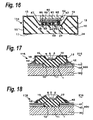
- FIG. 16 shows a submount 114 for a light-emitting device according to a further embodiment of the invention.
- the bonding materials 69 are isolated electrically from the other electrode 65 .
- bonding materials 69 are connected to a portion extended from the electrode 65 on the p-type semiconductor layer 64 . In this structure, no new electrode is needed for connecting the bonding materials 69 , and the fabrication process becomes simpler.
- FIGS. 17 and 18 show submounts 115 , 116 for light-emitting device 215 , 216 according to a further embodiment of the invention. These light-emitting devices have different types of the submount.
- the electrically conducting lines of the mount base 10 are not extended so as to have a section parallel to the metallic pattern 41 of the circuit board 300 .
- the submount 115 is mounted to the circuit board 300 by bonding the electrically conducting lines 13 , 16 of the mount base 10 with a solder 42 to the metallic pattern 41 of the circuit board 300 .
- the submount 115 is bonded at two sides thereof with solder 42 , while in the light-emitting device 200 shown in FIG. 2 the submount 100 is bonded with solder 42 at the bottom side thereof. Because the submount 115 does not have electrically conducting lines at the bottom thereof, the fabrication process becomes simpler. Further, because no solder layer is present between the submount 115 and the circuit board 300 , the size of the lighting device does not change due to the solder layer. Then the size in this direction can be set precisely, and the reliability of the thermal contact becomes higher.
- a top of the mount base 10 has planes inclined towards the circuit board 300 , and the electrically conducting lines 12 , 15 are extended thereon.
- the submount shown in FIG. 17 no solder layer is present between the submount 115 and the circuit board 300 , so that the fabrication process becomes simpler.
- the top of the submount is not flat and shoulders thereof become lower, the amount for the mount base can be decreased, and the size of the lighting device does not change due to the solder layer.
- the thermal contact 1 between the submount and the exposed area of the metallic plate is bonded with solder, while in the others the submount contacts with the exposed area of the metallic plate at the thermal contact 1 without an intermediate member between them.
- a metallic layer may be formed at the bottom of the mount base, and the submount may be bonded with solder to the exposed area of the metallic plate. Then the heat transfer efficiency may be increased further.
- the solder layer may be formed at the thermal contact, simultaneously in the reflow step as the electrical connection for the patterns.
- the position of the thermal contact is lower than the height of the pattern 41 of the circuit board.
- the thermal contact when the thermal contact is soldered, it can be prevented that the patterns 14 and 17 are short-circuited with solder.
- the contact portions at the most outside are still lower than the insulator layer of the circuit board 309 , 310 , so that the short-circuit at the thermal contact can be prevented surely.
- heat resistance is largest in the mount base having low thermal conductivity (0.3-10 W/mK).
- the heat resistance is proportional to the thickness of the mount base in the thickness direction and is inversely proportional to the thermal conductivity. Therefore, it is desirable that the thickness of the mount base below the LED chip is small.
- the decrease in the thickness of the mount base below the LED chip, or the main conduction path makes it difficult to form the mount base. Further, this decreases the strength of the mount base, so that the mount base is liable to be broken in a fabrication step for mounting the LED chip to the mount base. Then one or more grooves are formed on the mount base as explained below, so that the mount base can be formed easily while keeping the strength thereof, while the thermal resistance of the mount base can be decreased substantially.
- FIGS. 19A to 19D show a first example of a light-emitting device of having grooves on the mount base.
- a plurality of grooves are provided in parallel to each other on the bottom of the mount base 10 .
- an LED chip 50 is mounted face down on the bottom of a recess formed at the top of the mount base 10 of a submount 117 with bonding members 51 (flip chip).
- the mount base 10 is made of, for example, alumina, and has a protrusion 11 at the bottom thereof.
- three grooves 7 are formed in parallel at the center of the protrusion 11 .
- the grooves 7 are positioned to pass through an area 50 a , which is a projection image of the LED chip 50 in the vertical direction, in order to radiate heat efficiently. That is, the average thickness of the mount base 10 below the LED chip 50 becomes smaller, or the heat resistance at this area is decreased.
- solder layer 7 is formed between the bottom of the mount base 10 and the top of the circuit board 300 .
- the solder layer 30 also fills the grooves 7 , so that the average heat resistance between the LED chip 50 and the metallic plate 30 is further decreased by providing the solder layer 7 .
- a metallic film may be formed, for example, with copper plating having higher thermal conductivity (313 W/mK).
- the thermal resistance can be decreased further to a large extent by filling solder (thermal conductivity, 50 W/mK) into the grooves 7 . Because the thermal resistance of the mount base 10 below the LED chip 50 as the main conduction path is decreased, the temperature rise of the LED chip 50 can be decreased. Deposition or the like may be used for forming the metallic film.
- the metallic film may be made of copper, gold, silver or the like having a higher thermal conductivity than the mount base 10 and having good wetness for bonding.
- the filler for filling the grooves 7 as an auxiliary material for heat transfer is not limited to the above-mentioned solder.
- silver paste, silicone resin or the like may be used having higher thermal conductivity than the mount base 10 .
- the auxiliary material for heat transfer may be a soldered metallic wire such as a soldered copper wire.
- the grooves 7 may have side walls with a space between them increasing from the bottom to the opening thereof. Because the grooves 7 are broadened towards the openings thereof, the heat transfer from the mount base 10 to the metallic plate 30 of the circuit board is facilitated more than the grooves shown in FIG. 18C . Further, in this structure of the grooves 7 , the filler such as solder can be filled into the grooves 7 while suppressing the generation of bubbles. Therefore, this structure is advantageous for improving the heat transfer efficiency.
- FIGS. 20A to 20D show a modified example of the above-mentioned light-emitting device.
- the submount 117 shown in FIG. 19 has the protrusion 11 similarly to the submount 100 shown in FIG. 2 below the mount base 10 , while a submount 118 of this example without a protrusion may have grooves 7 at the bottom of the mount base 10 .
- the grooves 7 can be formed in parallel on the entire bottom.
- the circuit board 300 may have a thin insulator layer 40 (for example, equal to or smaller than about 100 micrometers), and the submount 118 may be mounted directly on the metallic plate 30 of the circuit board 300 by using a solder layer 43 formed by the bonding besides the bonding with solder 42 for the conduction layers.
- the plate 300 having a protrusion as shown in FIG. 4 may be used to contact with the bottom of the mount base 10 .
- a metallic member 25 a having protrusion to be fitted with the grooves 7 may be interposed between the mount base 10 and the metallic plate 30 .
- the conduction simulation is performed on three cases where the heating condition of the LED chip and the ambient temperature are kept the same.
- the grooves are not provided on the bottom of the mount base 10 ; in a second case the grooves 7 are provided on the mount base 10 at equal distance between them; and in a third case the grooves 7 are provided on the mount base 10 so that the total volume of the spaces in the grooves is the same as in the second case, but the grooves 7 are provided just below the bonding materials of the LED chip 5 .
- the simulation result shows that the temperature of the LED chip 5 is decreased in the order of the first case, second case and the third case. If the temperature of the LED chip 5 in the first case is set to 100 , it deceases to 83 for the second case and to 77 in the third case. Therefore, it is found that if the grooves 7 are provided just below the bonding materials 51 of the LED chip 50 , the heat transfer efficiency is improved further, and the temperature rise or the LED chip 50 can be decreased.
- FIG. 21 shows a light-emitting device of a further embodiment of the invention having a groove structure.
- the grooves 7 just below the bonding members 51 have the depth thereof deeper than the others.
- the thickness of the mount base 10 just below the LED chip 50 can be decreased further without decreasing the strength of the mount base 10 .
- the thermal resistance from the LED chip 50 to the metallic plate 30 can be decreased further, and the temperature rise of the LED chip 50 can be lowered.
- FIG. 22 shows a light-emitting device of another embodiment of the invention having a groove structure.
- the grooves 7 are arranged so that grooves 7 just below the bonding members 51 have the deepest depth, while grooves adjacent to one of the grooves having the deepest depth have depths decreasing stepwise with increase in the distance from the one of the grooves having the deepest depth.
- the thickness of the mount base 10 just below the LED chip 50 can be decreased further without deteriorating the strength of the mount base 10 . Then the thermal resistance from the LED chip 50 to the metallic plate 30 can be decreased further, and the temperature rise of the LED chip 50 can be lowered.
- FIG. 23 shows a light-emitting device of a further embodiment of the invention having a groove structure.
- a wide recess 71 is provided in the bottom of the mount base 10 below the LED chip 50
- grooves 7 are provided inside the recess 71 below the bonding materials 51 for the LED chip 50 . Because the recess 71 is wide and the depth of the grooves 7 is shallower than the counterparts in FIG. 22 , solder enters into and fills the grooves 7 more easily.
- FIGS. 24-27 show light-emitting devices of further embodiments of the invention having a groove structure and a plurality of LED chips 50 .
- the LED chips 50 are mounted adjacent to each other at a center of the mount base 10 , while grooves (or recesses) 7 are provided on the mount base 10 below the LED chips 50 .
- the grooves 7 have the same size.
- the depth of the groove 7 is deepest for the central LED chip 50 among the plurality of LED chips 50 and becomes shallower at both sides thereof according to the distance from the central groove for the central LED chip 50 .
- a plurality of grooves of narrow width are provided for each of the LED chips 50 , and the number or the density of the grooves below an LED chip 50 becomes highest for the central LED chip 50 .
- the light-emitting device shown in FIG. 27 has grooves 7 similarly to those shown in FIGS. 25 and 26 , but the grooves for the central LED chip 50 have the highest density and the deepest depth. Then, the central LED chip 50 can radiate heat efficiently, so that the temperature distribution of the LED chips 50 can be made even.
- FIGS. 28 to 31 show light-emitting devices of further embodiments of the invention having a groove structure similarly to those shown in FIGS. 24 to 27 , but having LED chips 55 mounted faceup.
- the LED chips 55 are mounted with a bonding material 57 such as a die bonding member or a plated layer.
- the electrical connection to electrodes 56 of the LED chips 55 is performed with wire bonding.
- the structure of the grooves 7 has an advantage to make temperature distribution even and to radiate heat efficiently, similarly to the above-mentioned light-emitting devices.
- FIGS. 32A and 32B show a submount 119 of a further embodiment of the invention having a groove structure.
- the submount 119 as shown in FIG. 32B , grooves 7 are formed on the bottom (or rear) thereof in vertical and transverse directions.
- solder or the like is interposed between the bottom of the submount 119 and the circuit board, and as shown above in FIG. 20D , it is filled into the grooves 7 .
- the grooves 7 can be formed vertically and transversely at a higher density than the counterparts shown in FIGS. 19 and 20 wherein the grooves 7 are arranged only in one direction, without decreasing the strength of the mount base 10 . Further, the heat can be radiated efficiently from the LED chip 50 to the circuit board 30 , and the temperature of the LED chip 50 can be decreased further. Further, because the grooves 7 are formed both vertically and transversely, air may leak easily from a side plane of the protrusion when solder. 53 is filled into the grooves 7 . Therefore, it becomes easier to fill solder into the grooves 7 . Further, because the thermal conductivity of solder 43 is higher than the mount base 10 , heat can be radiated efficiently. If the LED chip 50 is mounted above the crossings of the vertical and transverse grooves, the heat transfer can be performed more efficiently.
- FIG. 33 shows a submount of a further embodiment of the invention having a groove structure.
- Grooves 7 are provided to extend radially from the center of the protrusion 11 of the mount base 10 .
- a plurality of LED chips may be mounted.
- they may be mounted radially from the optical viewpoint. In such a case, when the above-mentioned radial grooves 7 are formed, the thickness of the mount base 10 just below the central LED chip among them can be decreased. Then, heat transfer from the LED chips to the metallic plate is improved, and the temperature of the LED chips can be lowered on the average.
- FIG. 34 shows a submount of a further embodiment of the invention having a groove structure.
- Grooves 7 are formed densely in some areas and coarsely in other areas at the bottom of the mount base 10 .
- the grooves 7 are formed densely at the central area so that the thickness of the mount base 10 just below the LED chip can be decreased, and heat transfer from the LED chips to the pattern plate is improved.
- FIGS. 35A and 35B show a submount 120 of a further embodiment of the invention having a groove structure.
- Deep wells 72 are formed on the bottom of the mount base 10 in an area 50 a just below the bonding members for the LED chip 50 , and grooves 7 are formed vertically and transversely through the wells 72 .
- Solder is filled into the grooves 7 and the wells 72 between the bottom of the mount base 10 and the metallic plate of the pattern plate (not shown).
- the numbers of the grooves 7 and the wells 72 and the positional relationship thereof are not limited to the example shown in FIGS. 35A and 35B .
- the thickness of the mount base 10 just below the LED chip can be decreased. Then, heat transfer from the LED chip to the metallic plate is improved, and the temperature of the LED chip can be lowered.
- FIG. 36 shows a submount of a further embodiment of the invention having a groove structure.
- Grooves 7 extend radially from a center of the protrusion 11 of the mount base 10 , and the other grooves 7 a are formed concentrically on the protrusion 11 .
- the above-mentioned grooves 7 , 7 a are formed radially around each of the LED chips to be mounted above areas 50 a . Then, the thickness of the mount base 10 just below LED chip(s) can be decreased. Then, heat transfer from the LED chip(s) to the circuit board is improved, and the temperature of the LED chip(s) can be lowered.
- FIG. 37 shows a submount of a further embodiment of the invention having a groove structure.
- Grooves 7 are formed radially around each of the LED chips to be mounted above areas 50 a . Then, when a plurality of LED chips are mounted, the thickness of the mount base 10 just below LED chips can be decreased. Then, heat transfer from the LED chips to the circuit board is improved, and the temperature of the LED chips can be lowered.
- FIGS. 38 and 39 show submounts of further embodiments of the invention having a groove structure.
- one spiral groove 7 is formed on the protrusion 11 on the bottom of the mount base 10
- one groove 7 is formed serpentinely on the protrusion 11 on the bottom of the mount base 10 .
- a soldered metallic wire such as a soldered copper wire may be inserted therein as an auxiliary material for facilitating heat transfer.
- a metallic wire or a copper wire has a higher thermal conductivity than the mount base 10 and than the solder. Therefore, by inserting the wire, the heat resistance can be decreased more. Because only one groove 7 is formed on the bottom of the protrusion 11 of the mount base 10 , it is easy to insert the wire in the groove 7 .
- FIGS. 40A and 40B show a submount 121 of a further embodiment of the invention having a groove structure.
- Two recesses (grooves) 73 are formed in parallel at the bottom of the mount base 10 outside an area just below the LED chip 50 .
- a solder layer 43 for bonding is interposed between the mount base 10 and the metallic plate 30 of the circuit board 300 .
- a length along the surface of the mount base 10 from the thermal contact (the solder layer 43 ) to an electrical contact (solder 42 ) between the electrically conducting line and the pattern 41 of the circuit board 300 becomes longer, so that electrical short-circuit between them can be suppressed.
- FIGS. 41A and 41B show a submount 122 of a further embodiment of the invention having a groove structure.
- Recesses 74 are formed similarly to, but having a larger size than the recesses 73 shown in FIGS. 40A and 40B .
- the recesses 74 have a bottom plane and two side planes extending between the bottom plane and the opening of the recess 74 , and the width of the recess becomes wider towards the opening thereof.
- a length along the surface of the mount base 10 from the thermal contact (the solder layer 43 ) to the electrical contact (solder 42 ) between the electrically conducting line and the metallic pattern 41 of the circuit board 300 becomes longer, so that electrical short-circuit between them can be suppressed. Further, an area for heat transfer is widened, and the heat transfer is improved. Further, the mount base 10 shown in FIGS. 41A and 41B can be fabricated easily with injection molding as a three-dimensional circuit board because the difference of the thickness of the mount base 10 is not so large, and the amount of a material for injection molding can be reduced.
- FIG. 42 shows a submount 123 of a further embodiment of the invention having a groove structure.
- the mount base 10 has recesses (grooves) 74 similar to those shown in FIGS. 41A and 41B and a metallic layer 74 a is formed on a side plate in the recess.
- the metallic layer 74 a may be formed with plating with silver or other metal such as copper or nickel. Alternatively, a white paint may be applied.
- the metallic layer 74 a can reflect a part or all of light emitted by the LED chip 50 and transmitting the mounting layer 10 .
- stray light in lateral directions can be taken out to the top plane, so that the efficiency of using the emitted light can be increased.
- FIG. 43 shows a submount 124 of a further embodiment of the invention having a groove structure.
- the mount base 10 has recesses 74 similar to those shown in FIGS. 41A and 41B . Further, air vents 75 are formed on the bottom of the mount base 10 from the inside of the recesses 74 to the side plane of the mount base 10 in a lateral direction. Then, heat transfer can be improved further due to the air vents 75 in the lateral direction.
- FIG. 44 shows a submount 125 of a further embodiment of the invention having a groove structure.
- the mount base 10 has recesses 74 and air vents 75 similar to those shown in FIG. 43 . Further, air vents 76 are formed from the inside of the recesses 74 to the top of the mount base 10 in the vertical direction. Then, heat transfer can be improved further due to the air vents in the vertical direction.
- the LED chip and the mount base in the submount are not limited to wire bonding, face down mounting and the like.
- the mount base is made of alumina, but it may also be made of a ceramic other than alumina or a resin.
- the filler for the grooves is not limited to solder, and a material such as silver paste or silicone resin may also be used having a higher thermal conductivity than the mount base.
- the number of the grooves and that of the LED chips are also not limited to the examples shown in the above-mentioned embodiments.
- an additional path for heat transfer is added besides the thermal contact between the submount and the circuit board in order to improve the heat transfer efficiency further. Then the injection current for LED chips can be increased further.
- FIG. 45 shows a light-emitting device according to a further embodiment of the invention
- FIGS. 46A and 46B show a structure of a submount 126 used for the light-emitting device shown in FIG. 45
- the light-emitting device shown in FIG. 45 has one or more submounts 126 interposed between a first plate 30 a and a second plate 30 b both provided for heat transfer.
- the submount 126 has a mount base 10 having electrically conducting lines 12 , 15 and an LED chip 5 mounted on the mount base 10 .
- the mount base 10 has a recess 435 on the top thereof, and two electrically conducting lines 12 , 15 are formed in the recess 435 and on the top plane of the mount base 10 .
- the shape of the mount base 10 is not limited to that shown in FIGS. 46A and 46B .
- it may have a flat top plane.
- the LED chip 5 is connected to the electrically conducting lines 12 , 15 at the bottom of the recess 435 with bonding materials 434 between them, as shown in FIG. 46B , and the submounts 126 are mounted in the light-emitting device as shown in FIG. 45 .
- the first plate 30 a is a circuit board, mentioned above, having a metallic plate 411 , an insulator layer 412 and a metallic pattern 413 formed on the insulator layer 412 .
- Two ends of the electrically conducting line 12 , 15 on the top plane of the mount base 10 are used as lands 432 for electrical connection as the positive and negative terminals.
- the lands 432 of the submount 126 and the patterns 413 of the first plate 30 a are bonded with solder 415 .
- a portion of the plate 30 a opposing to the LED chip 5 has an opening 410 in correspondence to the recess.
- a device for converting wavelength of incident light such as a fluorescent material may be set in the opening.
- the second plate 30 b is made of a metallic plate.
- a land 436 isolated electrically is formed for soldering on the bottom (rear) plane of the mount base 10 , and it is bonded with solder 425 to the second plate 30 b .
- the second plate 30 b has thermal conduction portions 424 having planes opposing to the first plate 30 a .
- the thermal conduction portions 424 of the second plate 30 b contact with the first plate 30 a or, preferably, are bonded thereto with soldering.
- the thermal conduction portions 424 may be provided as separate members to be bonded with the first and second plates 30 a and 30 b with solder or the like, or may be parts of the first or second plate 30 a , 30 b . Further, the thermal conduction portions 424 may contact with or be bonded to sides of the submounts 126 .
- the mount base 10 is made of a ceramic material such as aluminum nitride having good thermal conductivity, the heat can be conducted more efficiently, and the temperature of the ELD chip 5 can be decreased more.
- two plates 30 a , 30 b used for heat transfer are mounted above and below the submount(s) 126 , but the setting of the plates 30 a and 30 b are not limited to this example.
- the mount base 10 is for example a molded-interconnect-device (MID) plate
- MID molded-interconnect-device
- the two plates for heat transfer can be set at appropriate positions according to the requirements on the space where the light-emitting device is used, for example, on two planes or on a rear plane and a side plane. This also applies to following embodiments explained below.
- third and fourth plates for heat transfer may be set further at two sides of the submounts 126 . This improves heat transfer further, and the chip temperature is decreased further.
- FIG. 47 shows a light-emitting device according to a further embodiment of the invention
- FIG. 48 shows a section of the light-emitting device observed in the right side in FIG. 47
- FIGS. 49A , 49 B and 50 A, 50 B show structures of a submount 127 and a first plate 30 a for heat transfer of the light-emitting device shown in FIG. 47 , respectively.
- the light-emitting device of this embodiment is similar to that shown in FIGS. 45 and 46 except following points.
- a portion of the metallic plate 411 of the first plate 30 a is exposed by removing a part of the insulator layer 412 or no electric conduction pattern is formed thereon, so as to make the metallic plate 411 contact with the top of the mount base 10 .
- a groove 437 is formed on the top of the mounting plane 10 , and lands 432 to be extended to the electrically conducting line 12 , 15 are formed in the groove 437 .
- the portion of the first plate 30 a on which the pattern 413 is formed so as to fit to the groove 437 on the top plane of the mount base 10 .
- the lands 432 are bonded with solder to the pattern 413 on the first plate 30 a .
- the first plate 30 a is bonded with solder 416 to a pattern 438 formed at the top of the mount base 10 .
- a portion of the plate 30 a opposing to the LED chip 5 has an opening 410 .
- the second plate 30 b is a metallic plate having a higher thermal conductivity than the circuit board, the heat diffused in the mount base 10 made of a ceramic material can be diffused further, and the temperature of the LED chip 5 can be lowered further.
- the heat transfer can be performed more efficiently, and the temperature of the LED chip 5 can be lowered further. Further, because the circuit boards are used for heat transfer, the degree of freedom on the electrical connection of the submount can be increased.
- FIG. 51 shows a light-emitting device according to a further embodiment of the invention
- FIGS. 52A and 52B show a submount 128 of the light-emitting device.
- the mount base 10 of the submount 128 has a multi-layer structure made of flat plates and has electrically conducting lines 12 and 15 .
- the shape of the mount base 10 is not limited to be the flat plane, and it may be a plate having a recess or the like.
- the electrically conducting lines 12 and 15 extend from the top of the mount base 10 through throughholes 12 a , 15 a to an inner layer and further to an side plane thereof and to a part of the bottom of the mount base 10 .
- a land 436 is formed for soldering at the bottom of the mount base 10 is formed at the bottom of the submount 128 and is bonded to the pattern 413 on the first plate 30 a , but isolated electrically.
- An LED chip 5 is mounted with a bonding material 434 on the electrically conducting lines 21 , 15 of the mount base 10 .
- the first plate 30 a has a metallic plate 411 , an insulator layer 412 and a metallic pattern 413 formed on the insulator layer 412 .
- a portion of the metallic plate 411 of the first plate 30 a is exposed by removing a part of the insulator layer 412 on which no electric conduction pattern is formed, so as to make the metallic plate contact with the top plane of the mount base 10 .
- the first plate 30 a is bonded with solder 416 to the land 436 at the bottom plane of the mount base 10 . Further, the land at an end of the pattern 413 of the first plate 30 a is connected with solder 415 to the land 432 at an end of the pattern 413 of the mount base 10 .
- the second plate 30 b for heat transfer is a metallic plate made of copper, and it is bonded to the top plane of the mount base 10 in this embodiment.
- the metallic plate is made of copper, but is not limited thereto.
- An opening 420 is provided in a portion of the second plate 30 a opposing the LED chip 5 . It is preferable that the side of the opening 420 is tapered, but not limited to the tapered shape. In this example, silver is deposited on the surface of the tapered portion, and the silver film is polished.
- mount base 10 is made of a ceramic material, it is preferable that a plane in contact with the second plate 30 b is metallized, for example with tungsten, and the metallized portion for heat transfer may be bonded directly without soldering to the second plate 30 b.
- the heat diffused in the mount base 10 made of a ceramic material having high thermal conductivity is led through the metallic plate having high thermal conductivity, so that the temperature of the LED chip 5 can be lowered further.
- the pattern 413 can be formed at both sides of the first plate 30 a opposing the submount 128 , and the second plate usually fixed to an external device may not have a pattern. Then, it is advantageous that the design of electrical insulation has a high freedom.
- FIG. 53 show a light-emitting device according to a further embodiment of the invention
- FIGS. 54A and 54B show a submount 129 thereof.
- a circuit board 30 a having a metallic plate 411 , an insulator layer 412 and the pattern 413 is provided at the bottom plane of the submount 129 .
- a recess 435 and a groove 437 are formed on the top of the submount 129 , and electrically conducting line 12 , 15 are formed on the bottom of the groove 437 and on the recess 435 . Because the electrically conducting lines 12 and 15 formed on the submount 129 are formed in the groove 437 , they do not contact with the second plate 30 b .
- a metallic plate as the second plate 30 b has an opening 420 of about the same size as the opening of the recess 435 on which the LED chip 5 is mounted.
- a cover 426 made of a transparent material or a material such as a fluorescent material converting the wavelength of incident light emitted by the LED chip 5 can be set in the opening 420 of the second plate 30 b , or it can be used as a member for setting the fluorescent material.
- the heat generated in the LED chip 5 is conducted through the mount base 10 of the submount 129 to the second plate 30 b and is radiated from the surface of the second plate 30 b . Because the heat is also radiated from the second plate 30 b , the heat transfer of the submount 129 is improved, and the temperature of the LED chip 5 is decreased. Therefore, the light-emitting device has a longer life. Further, because a larger current can be flown, the light intensity can be increased. Because the second plate is also used as a member for holding the fluorescent cover, the fabrication cost therefor can be decreased.
- FIGS. 55 and 56A , 56 B show a light-emitting device according to a further embodiment of the invention.
- a mount base 10 of a submount 130 is made of a resin or a ceramic, and a plurality of thermal vias 439 made of a metal such as copper, solder or gold having a good thermal conductivity are formed in the mount base 10 .
- the thermal vias 439 do not contact with or is insulated electrically from the electrically conducting line 12 , 15 formed on the submount 130 .
- the top planes of the thermal vias 439 are exposed at the top plane of the submount 130 .
- a recess 435 and a groove 437 are formed on the top of the submount 130 , and electrically conducting lines 12 , 15 are formed on the bottom thereof.
- a metallic plate used as the second plate 30 b is set on a top plane of the submount 130 opposing to the top of the circuit board used as the first plate 30 a.
- the second plate 30 b has an opening 420 having about the same size as the opening of the recess 435 on which the LED chip 5 is mounted.
- the second plate 30 b of the mount base 10 is bonded with solder to the thermal vias 439 formed in the mount base 10 .
- a cover 426 made of a transparent material or a material such as a fluorescent material converting the wavelength of the incident light emitted by the LED chip 5 can be set in the opening 420 of the second plate 30 b , or it can be used as a member for setting the fluorescent material. Because the electrically conducting lines 12 and 15 are formed in the groove 437 , they do not contact with the second plate 30 b .
- the thermal via 439 may be fabricated by forming a hole from above the top plane of the submount 130 , by plating gold at the side of the hole and by filling solder therein.
- the thermal vias are positioned near the LED chip 5 than the side plane of the submount 130 , the heat generated by the LED chip 5 is likely to conduct through the thermal vias 439 than the side plane of the submount 130 . Thus, the heat is conducted from the mount base 10 of the submount through the thermal vias 439 to the second plate 30 b to be radiated from the surface thereof.
- the heat is also radiated from the second plate for heat transfer, the heat transfer of the submount is improved, and the temperature of the LED chip is decreased. Therefore, the light-emitting device has a longer life. Further, because a larger current can be flown, the light intensity can be increased. Because the second plate is also used as a member for holding the fluorescent cover, the fabrication cost can be decreased.
- FIGS. 57A and 57B show a submount 131 and FIGS. 58A and 58B shows a light-emitting device with the submount 131 according to a further embodiment of the invention.
- a metallic panel 436 a is provided on the generally whole bottom plane of the submount 131 .
- Thermal vias 439 a to 439 f are embedded in the mount base 10 , and the bottom planes thereof contact with the top of the metallic panel 436 a .
- the bottom plane of the metallic panel 436 a is bonded with solder 425 to a metallic plate used as the second plate 30 b for heat transfer. Therefore, each of the thermal vias 439 a to 439 f is connected thermally to the second plate 30 b closely.
- the bottom of the thermal vias 439 a to 439 f may be extended to the bottom plane of the second plane 30 b .
- the tops of the thermal vias 439 a to 439 d embedded around the four corners of the mount base 10 are exposed at the top plane of the submount 131 without contacting with the electrically conducting lines 12 , 15 and contacts with a metallic plate 411 of the first plate 30 a .
- the electrically conducting lines 12 , 15 formed on a recess 435 of the submount 131 are extended to the top plane of the mount base 10 and are connected to pads 432 .
- the circuit board used as the first plate 30 a has a metallic plate 411 , an insulator layer 412 and a pattern layer 413 , and the pattern of the pattern layer 413 faces the top of the submount 131 .
- the pattern layer 413 is connected with solder 415 to the pads 432 connected to the electrically conducting lines 12 , 15 .
- the tops of the thermal vias 439 a to 439 d exposed at the top plane of the submount 131 are connected with solder to the metallic plate 411 of the first plate 30 a .
- the metallic plate 411 is also used as a jig for setting a fluorescent cover 426 .
- the second plate 30 b for heat transfer and the submount 131 are connected to each other over a large area to facilitate head conduction through the main heat transfer path.
- a plate at the bottom side of a submount is fixed generally to the main body of the device after an insulating processing. In the structure of this embodiment, this corresponds to the second plate 30 b . Because it is insulated electrically from the LED chip 5 , an insulating process is not needed, or the fabrication cost can be decreased. Further, the heat resistance between the second plate 30 b and the main body of the device can be decreased, and the heat transfer can be performed efficiently.
- FIGS. 59A , 59 B and 59 C show a light-emitting device according to a further embodiment of the invention.
- a plurality of layers of metallic foils 431 a (for heat transfer) having high thermal conductivity are provided in a mount base 10 a of a submount 132 . It is not necessary that the metallic foils are arranged horizontally, but that they are arranged desirably with good balance for facilitating head conduction. They are not exposed to the outside of the submount 132 .
- a metallic plate 436 b has electrically conducting line 431 and an insulator layer 430 b formed successively thereon, and they are arranged on the bottom plane of the submount 132 . They extend to the lateral side to provide pads 432 at the top plane thereof. Electrically conducting lines 431 b are formed on a recess 435 formed at the center of the top plane of the submount 132 to connect the metallic foils 431 a and the electrically conducting line 431 .
- the pads 432 are connected with wire bonding to the pattern 413 in the first plate 30 b .
- the technique for electrical connection is not limited. In the example shown in FIGS. 59A to 59C , an end of a wire 432 b is bonded, while the other end thereof is connected with solder 415 to the pattern 413 .
- the metallic foils 431 a to be connected to p and n electrodes of the LED chip 5 and the metallic layer 431 b at the sides of the recess 435 of the submount 132 are independent of each other, and they are not connected between the p and n sides.
- the patterns 431 b may be formed by forming a pattern of the metallic foil 431 a on a ceramic foil which has been formed to have a predetermined shape, by layering the metallic foils on the ceramic foils on the metallic plate 436 b , and by curing it.
- the heat generated in the LED chip is conducted to the entire submount through the patterns for heat transfer, so that the heat transfer from the surface of the submount is accelerated. Because no pattern is present on the first plate for heat transfer opposing to the bottom plane of the submount, the contact area between them becomes wide, so that the heat transfer to the circuit board is enhanced, or the heat transfer through this path is increased.
- the temperature of the LED chip can be lowered to give a longer life of the light-emitting device. Because a lager electrical current can be flown through the LED chip, the light intensity can be increased.
- FIG. 60A shows a light-emitting device according to a further embodiment of the invention, wherein the submount has the structure shown in FIGS. 59A to 59C .
- a plate 30 b provided on the top plane of the submount is also used as a frame for setting a fluorescent material 426 and a lens 427 for light control.
- Thermal vias 439 are formed through the foils 431 a , but not exposed at the top of the submount.
- the tops of the thermal vias 439 have gold layers, and the frame 30 b for fixing the lens is bonded with solder thereto.
- the top plate 30 b may also be used only to set a fluorescent cover 426 , while the lens 427 may be separated therefrom.
- the reference number 440 represents an electronics part.
- the thermal vias 439 may be exposed at the top of the submount.
- the circuit board is set on the top plate, and the thermal vias as electrodes are connected to the circuit board or the first plate for heat transfer.
- the heat transfer to the submount becomes even through the thermal vias, and the heat transfer in the upper direction to the second plate for heat transfer is also accelerated
- a similar advantage is obtained by providing a metallic plate for heat transfer on the top of the submount, but the thermal vias can accelerate heat transfer more.
- heat transfer is accelerated more by using the patterns for heat transfer and the thermal vias.
- the submount 133 is used, but the type thereof is not limited thereto.
Abstract
Description
Claims (3)
Applications Claiming Priority (7)
| Application Number | Priority Date | Filing Date | Title |
|---|---|---|---|
| JP2003-148050 | 2003-05-26 | ||
| JP2003148050 | 2003-05-26 | ||
| JP2003-298007 | 2003-08-21 | ||
| JP2003298007A JP4123105B2 (en) | 2003-05-26 | 2003-08-21 | Light emitting device |
| JP2003-394451 | 2003-11-25 | ||
| JP2003394451A JP2005158957A (en) | 2003-11-25 | 2003-11-25 | Light emitting device |
| PCT/JP2004/007535 WO2004105142A1 (en) | 2003-05-26 | 2004-05-26 | Light-emitting device |
Publications (2)
| Publication Number | Publication Date |
|---|---|
| US20070007540A1 US20070007540A1 (en) | 2007-01-11 |
| US7495322B2 true US7495322B2 (en) | 2009-02-24 |
Family
ID=33479651
Family Applications (1)
| Application Number | Title | Priority Date | Filing Date |
|---|---|---|---|
| US10/558,360 Active 2024-11-06 US7495322B2 (en) | 2003-05-26 | 2004-05-26 | Light-emitting device |
Country Status (4)
| Country | Link |
|---|---|
| US (1) | US7495322B2 (en) |
| EP (2) | EP1627437B1 (en) |
| TW (1) | TWI253765B (en) |
| WO (1) | WO2004105142A1 (en) |
Cited By (57)
| Publication number | Priority date | Publication date | Assignee | Title |
|---|---|---|---|---|
| US20070237197A1 (en) * | 2006-04-05 | 2007-10-11 | Sharp Kabushiki Kaisha | Semiconductor light emitting device |
| US20070268703A1 (en) * | 2006-05-22 | 2007-11-22 | Valeo Vision | Heat dissipation component and diode lighting and/or signalling device equipped with a component of this type |
| US20080149373A1 (en) * | 2006-12-21 | 2008-06-26 | Yong Suk Kim | Printed circuit board, light emitting apparatus having the same and manufacturing method thereof |
| US20090039380A1 (en) * | 2007-08-10 | 2009-02-12 | Matsushita Electric Works, Ltd. | Package and semiconductor device |
| US20090097233A1 (en) * | 2005-08-23 | 2009-04-16 | Kabushiki Kaisha Toshiba | Light-emitting device, backlight using same, and liquid crystal display |
| US20090154180A1 (en) * | 2007-12-18 | 2009-06-18 | Sl Seobong | Heat-dissipating apparatus |
| US20090224278A1 (en) * | 2004-12-10 | 2009-09-10 | Matsushita Electric Industrial Co., Ltd. | Semiconductor light-emitting device, light-emitting module and lighting unit |
| US20090284932A1 (en) * | 2008-03-25 | 2009-11-19 | Bridge Semiconductor Corporation | Thermally Enhanced Package with Embedded Metal Slug and Patterned Circuitry |
| US20090314534A1 (en) * | 2006-06-15 | 2009-12-24 | Yoichi Matsuoka | Electronic component |
| US20100001309A1 (en) * | 2008-03-25 | 2010-01-07 | Bridge Semiconductor Corporation | Semiconductor chip assembly with post/base heat spreader and horizontal signal routing |
| US20100052005A1 (en) * | 2008-03-25 | 2010-03-04 | Lin Charles W C | Semiconductor chip assembly with post/base heat spreader and conductive trace |
| US20100075448A1 (en) * | 2008-03-25 | 2010-03-25 | Bridge Semiconductor Corporation | Method of making a semiconductor chip assembly with a post/base/cap heat spreader |
| US20100072511A1 (en) * | 2008-03-25 | 2010-03-25 | Lin Charles W C | Semiconductor chip assembly with copper/aluminum post/base heat spreader |
| US20100096662A1 (en) * | 2008-03-25 | 2010-04-22 | Bridge Semiconductor Corporation | Semiconductor chip assembly with post/base heat spreader and signal post |
| US20100127300A1 (en) * | 2008-11-27 | 2010-05-27 | Samsung Electro-Mechanics Co., Ltd. | Ceramic package for headlamp and headlamp modul having the same |
| US20100133558A1 (en) * | 2004-11-05 | 2010-06-03 | Neobulb Technologies, Inc. | Flip chip type led lighting device manufacturing method |
| US20100148206A1 (en) * | 2006-10-06 | 2010-06-17 | Industrial Technology Research Institute | LED package and method of assembling the same |
| US20100148196A1 (en) * | 2005-09-20 | 2010-06-17 | Matsushita Electric Works, Ltd. | Led lighting fixture |
| US20100155769A1 (en) * | 2008-03-25 | 2010-06-24 | Bridge Semiconductor Corporation | Semiconductor chip assembly with base heat spreader and cavity in base |
| US20100155768A1 (en) * | 2008-03-25 | 2010-06-24 | Bridge Semiconductor Corporation | Semiconductor chip assembly with post/base heat spreader and cavity in post |
| US20100163921A1 (en) * | 2008-03-25 | 2010-07-01 | Bridge Semiconductor Corporation | Semiconductor chip assembly with aluminum post/base heat spreader and silver/copper conductive trace |
| US20100181594A1 (en) * | 2008-03-25 | 2010-07-22 | Lin Charles W C | Semiconductor chip assembly with post/base heat spreader and cavity over post |
| US20100230707A1 (en) * | 2006-03-03 | 2010-09-16 | Kyung Ho Shin | Light-emitting diode package and manufacturing method thereof |
| US20100246135A1 (en) * | 2009-03-31 | 2010-09-30 | Sanyo Electric Co., Ltd. | Electronic device |
| US20100289054A1 (en) * | 2008-03-25 | 2010-11-18 | Bridge Semiconductor Corporation | Semiconductor chip assembly with post/base heat spreader and adhesive between base and terminal |
| US20100302789A1 (en) * | 2009-05-28 | 2010-12-02 | Qing Li | LED Light Source Module and Method for Producing the Same |
| US20100327310A1 (en) * | 2008-03-25 | 2010-12-30 | Lin Charles W C | Semiconductor chip assembly with post/base/flange heat spreader and cavity in flange |
| US20110037094A1 (en) * | 2008-03-25 | 2011-02-17 | Bridge Semiconductor Corporation | Semiconductor chip assembly with bump/base heat spreader and cavity in bump |
| US20110049558A1 (en) * | 2008-03-25 | 2011-03-03 | Lin Charles W C | Semiconductor chip assembly with post/base heat spreader, signal post and cavity |
| US20110056734A1 (en) * | 2009-09-08 | 2011-03-10 | Andrews Peter S | Electronic device submounts with thermally conductive vias and light emitting devices including the same |
| US20110065241A1 (en) * | 2008-03-25 | 2011-03-17 | Bridge Semiconductor Corporation | Method of making a semiconductor chip assembly with a bump/base heat spreader and a dual-angle cavity in the bump |
| US20110089465A1 (en) * | 2008-03-25 | 2011-04-21 | Lin Charles W C | Semiconductor chip assembly with post/base heat spreader with esd protection layer |
| US20110096526A1 (en) * | 2007-12-26 | 2011-04-28 | Kyocera Corporation | Light Emitting Device and Illumination Device |
| US20110104856A1 (en) * | 2008-03-25 | 2011-05-05 | Bridge Semiconductor Corporation | Method of making a semiconductor chip assembly with a post/base/post heat spreader |
| US20110104855A1 (en) * | 2008-03-25 | 2011-05-05 | Bridge Semiconductor Corporation | Method of making a semiconductor chip assembly with a post/base heat spreader with an ESD protection layer |
| US20110133236A1 (en) * | 2009-12-03 | 2011-06-09 | Takahiko Nozaki | Semiconductor light emitting device |
| US20110151626A1 (en) * | 2008-03-25 | 2011-06-23 | Lin Charles W C | Method of making a semiconductor chip assembly with a post/base/post heat spreader and asymmetric posts |
| US20110163348A1 (en) * | 2008-03-25 | 2011-07-07 | Bridge Semiconductor Corporation | Semiconductor chip assembly with bump/base heat spreader and inverted cavity in bump |
| US20110183472A1 (en) * | 2008-03-25 | 2011-07-28 | Bridge Semiconductor Corporation | Method of making a semiconductor chip assembly with a post/base heat spreader and a plated through-hole |
| US20110180819A1 (en) * | 2008-09-16 | 2011-07-28 | Koninklijke Philips Electronics N.V. | Light-emitting arrangement |
| US20110198662A1 (en) * | 2008-03-25 | 2011-08-18 | Bridge Semiconductor Corporation | Semiconductor chip assembly with post/base heat spreader and multilevel conductive trace |
| US20110227122A1 (en) * | 2008-03-25 | 2011-09-22 | Bridge Semiconductor Corporation | Semiconductor chip assembly with post/base heat spreader with thermal via |
| US20110266586A1 (en) * | 2010-04-29 | 2011-11-03 | Advanced Optoelectronic Technology, Inc. | Led package and manufacturing method thereof |
| US8125000B2 (en) * | 2008-05-23 | 2012-02-28 | Lg Innotek Co., Ltd. | Light emitting device package having dual recessed substrate |
| US8153477B2 (en) | 2008-03-25 | 2012-04-10 | Bridge Semiconductor Corporation | Method of making a semiconductor chip assembly with a post/dielectric/post heat spreader |
| US20120187862A1 (en) * | 2007-10-31 | 2012-07-26 | Jeffrey Carl Britt | Light emitting die (led) packages and related methods |
| US8232576B1 (en) | 2008-03-25 | 2012-07-31 | Bridge Semiconductor Corporation | Semiconductor chip assembly with post/base heat spreader and ceramic block in post |
| US20120262643A1 (en) * | 2011-04-14 | 2012-10-18 | Kweon Young-Min | Backlight unit and liquid crystal display device including the same |
| US8304292B1 (en) | 2009-08-06 | 2012-11-06 | Bridge Semiconductor Corporation | Method of making a semiconductor chip assembly with a ceramic/metal substrate |
| US8354283B2 (en) | 2008-03-25 | 2013-01-15 | Bridge Semiconductor Corporation | Method of making a semiconductor chip assembly with a bump/base/ledge heat spreader, dual adhesives and a cavity in the bump |
| US20130188359A1 (en) * | 2010-10-11 | 2013-07-25 | Lg Innotek Co., Ltd. | Radiant heat circuit board, method of manufacturing the same, heat generating device package having the same, and backlight |
| US20130298396A1 (en) * | 2011-11-09 | 2013-11-14 | Xiaofeng Bi | Method of making a heat radiating structure for high-power led |
| DE102013206996A1 (en) * | 2013-04-18 | 2014-10-23 | Robert Bosch Gmbh | Heat pump with a control unit and separable heat sink |
| US8950897B2 (en) | 2011-11-21 | 2015-02-10 | Panasonic Corporation | Light-emitting device and lighting apparatus |
| US20150305164A1 (en) * | 2013-01-09 | 2015-10-22 | Shenzhen China Star Optoelectrics Technology Co., Ltd. | Backlight Module, Printed Circuit Board Used For Backlight Module, And Manufacturing Method For The Same |
| US9303861B2 (en) | 2009-09-14 | 2016-04-05 | Us Vaopto, Inc. | Light emitting diode light source modules |
| US9685593B2 (en) | 2013-11-25 | 2017-06-20 | Osram Opto Semiconductors Gmbh | Housing for a semiconductor chip, housing composite, semiconductor component and method of producing a semiconductor component |
Families Citing this family (57)
| Publication number | Priority date | Publication date | Assignee | Title |
|---|---|---|---|---|
| DE102004064150B4 (en) * | 2004-06-29 | 2010-04-29 | Osram Opto Semiconductors Gmbh | Electronic component with housing with conductive coating for ESD protection |
| US7683393B2 (en) * | 2004-12-07 | 2010-03-23 | Ngk Spark Plug Co., Ltd. | Wiring substrate for mounting light emitting element |
| CN100539219C (en) * | 2005-04-28 | 2009-09-09 | 皇家飞利浦电子股份有限公司 | Comprise the light source that is arranged on the LED in the recess |
| KR101065076B1 (en) * | 2005-05-07 | 2011-09-15 | 삼성전자주식회사 | Submount for light emitting device |
| KR101093324B1 (en) * | 2005-05-30 | 2011-12-14 | 엘지이노텍 주식회사 | Back light unit having light emitting diode |
| CH705956B1 (en) * | 2005-06-23 | 2013-07-15 | Lvmh Swiss Mft Sa | A display device of numeric or alphanumeric symbols. |
| WO2007034575A1 (en) * | 2005-09-20 | 2007-03-29 | Matsushita Electric Works, Ltd. | Light emitting device |
| EP1932401A1 (en) * | 2005-09-29 | 2008-06-18 | Philips Intellectual Property & Standards GmbH | Method for fixing a light-emitting diode to a metallic heat-radiating element |
| KR101181112B1 (en) | 2005-10-27 | 2012-09-14 | 엘지이노텍 주식회사 | Light-emitting diode, manufacturing method for the light-emitting diode and light-emitting diode module |
| US7732233B2 (en) | 2006-07-24 | 2010-06-08 | Touch Micro-System Technology Corp. | Method for making light emitting diode chip package |
| TWI418054B (en) * | 2006-08-08 | 2013-12-01 | Lg Electronics Inc | Light emitting device package and method for manufacturing the same |
| US20080054274A1 (en) * | 2006-08-30 | 2008-03-06 | Unity Opto Technology Co., Ltd. | Edge-emitting light-emitting diode |
| JPWO2008029892A1 (en) * | 2006-09-07 | 2010-01-21 | パナソニック株式会社 | Laser light source, surface light source, and liquid crystal display device |
| DE102006059702A1 (en) * | 2006-09-29 | 2008-04-03 | Osram Opto Semiconductors Gmbh | Opto-electronic element has metal core plate, metal core, dielectric layer applied on metal core and electrically conductive layer applied on dielectric layer and element also has chip carrier connected with metal core plate |
| US20100163890A1 (en) * | 2007-02-14 | 2010-07-01 | Michael Miskin | Led lighting device |
| US8421088B2 (en) * | 2007-02-22 | 2013-04-16 | Sharp Kabushiki Kaisha | Surface mounting type light emitting diode |
| TW200843135A (en) * | 2007-04-23 | 2008-11-01 | Augux Co Ltd | Method of packaging light emitting diode with high heat-dissipating efficiency and the structure thereof |
| US20090023234A1 (en) * | 2007-07-17 | 2009-01-22 | Hung-Tsung Hsu | Method for manufacturing light emitting diode package |
| DE102007053849A1 (en) | 2007-09-28 | 2009-04-02 | Osram Opto Semiconductors Gmbh | Arrangement comprising an optoelectronic component |
| TW200930948A (en) * | 2007-10-09 | 2009-07-16 | Koninkl Philips Electronics Nv | Light emitting device package, light output system and light output method |
| DE102008021618A1 (en) * | 2007-11-28 | 2009-06-04 | Osram Opto Semiconductors Gmbh | Chip arrangement, connection arrangement, LED and method for producing a chip arrangement |
| EP2096685A1 (en) * | 2008-02-28 | 2009-09-02 | Robert Bosch Gmbh | LED module with cooling bodies containing mounting elements |
| US8080827B2 (en) * | 2008-07-31 | 2011-12-20 | Bridgelux, Inc. | Top contact LED thermal management |
| TWI382565B (en) * | 2008-10-15 | 2013-01-11 | Young Optics Inc | Light emitting diode apparatus and optical engine using the same |
| US8203266B2 (en) * | 2008-10-23 | 2012-06-19 | Hamamatsu Photonics K.K. | Electron tube |
| US8729591B2 (en) * | 2009-02-13 | 2014-05-20 | Tsmc Solid State Lighting Ltd. | Opto-electronic device package with a semiconductor-based sub-mount having SMD metal contacts |
| KR101064098B1 (en) * | 2009-02-23 | 2011-09-08 | 엘지이노텍 주식회사 | Light emitting device package and manufacturing method thereof |
| JP5146356B2 (en) * | 2009-02-24 | 2013-02-20 | 豊田合成株式会社 | Light emitting device and manufacturing method thereof |
| JP5936810B2 (en) * | 2009-09-11 | 2016-06-22 | ローム株式会社 | Light emitting device |
| DE102009054840A1 (en) * | 2009-12-17 | 2011-06-22 | Poly-Tech Service GmbH, 67681 | Illuminant with a plurality of LEDs |
| DE102010029529A1 (en) * | 2010-05-31 | 2011-12-01 | Osram Gesellschaft mit beschränkter Haftung | Component carrier i.e. metal core printed circuit board, for LED lighting device, has heat guide element arranged on mounting plate and in contact with electronic component, where heat guide element passes through heat sink |
| KR101779205B1 (en) * | 2010-10-06 | 2017-09-26 | 엘지이노텍 주식회사 | The radiant heat circuit board and the heat generating device package having the same |
| BR112013009010A2 (en) * | 2010-10-13 | 2017-10-31 | Ceram Gmbh | process for joining two sections to be joined, ie ceramic with metal / ceramic with a laser beam |
| TWI430429B (en) * | 2010-12-24 | 2014-03-11 | Au Optronics Corp | Light-emitting module |
| US9704793B2 (en) | 2011-01-04 | 2017-07-11 | Napra Co., Ltd. | Substrate for electronic device and electronic device |
| DE102011012924A1 (en) * | 2011-03-03 | 2012-09-06 | Osram Opto Semiconductors Gmbh | Support for an optoelectronic structure and optoelectronic semiconductor chip with such a support |
| US8829557B2 (en) * | 2011-04-08 | 2014-09-09 | Lg Innotek Co., Ltd. | Light emitting device module and lighting system including the same |
| KR101799449B1 (en) * | 2011-05-04 | 2017-11-20 | 엘지이노텍 주식회사 | Light emitting device module and lighting apparatus including the same |
| CN102842666B (en) * | 2011-06-22 | 2015-03-18 | 赛恩倍吉科技顾问(深圳)有限公司 | LED (Light Emitting Diode) flip chip structure and manufacturing method thereof |
| US8878221B2 (en) * | 2011-08-19 | 2014-11-04 | Lg Innotex Co., Ltd. | Light emitting module |
| CN111048650A (en) * | 2012-05-23 | 2020-04-21 | 亮锐控股有限公司 | Surface mountable semiconductor device |
| US8933473B1 (en) * | 2012-06-01 | 2015-01-13 | Valery Dubin | Method, apparatus and system for providing light source structures on a flexible substrate |
| DE102012106982A1 (en) | 2012-07-31 | 2014-02-06 | Osram Opto Semiconductors Gmbh | Process for the production of a light source |
| US9420682B2 (en) * | 2013-02-25 | 2016-08-16 | Abl Ip Holding Llc | Heterogeneous thermal interface |
| CN105191027B (en) * | 2013-05-08 | 2019-09-03 | 皇家飞利浦有限公司 | Mounting layer for cooling structure |
| CN104251417A (en) * | 2013-06-28 | 2014-12-31 | 展晶科技(深圳)有限公司 | Light source module |
| JP6623508B2 (en) * | 2014-09-30 | 2019-12-25 | 日亜化学工業株式会社 | Light source, method of manufacturing and mounting method |
| CZ2014761A3 (en) * | 2014-11-06 | 2016-01-06 | Varroc Lighting Systems, s.r.o. | Light source |
| TW201526315A (en) * | 2015-02-17 | 2015-07-01 | Xiu-Zhang Huang | Flip-chip LED and manufacturing method thereof |
| DE102015205354A1 (en) * | 2015-03-24 | 2016-09-29 | Osram Gmbh | Optoelectronic assembly and method for manufacturing an optoelectronic assembly |
| US10374134B2 (en) | 2015-05-29 | 2019-08-06 | Nichia Corporation | Light emitting device, method of manufacturing covering member, and method of manufacturing light emitting device |
| DE102016213069A1 (en) * | 2016-07-18 | 2018-01-18 | Osram Gmbh | LEDS ARRANGEMENT |
| DE102017000185A1 (en) * | 2017-01-12 | 2018-07-12 | Osram Gmbh | A light emitting assembly and method of making a light emitting assembly |
| JP7231809B2 (en) | 2018-06-05 | 2023-03-02 | 日亜化学工業株式会社 | light emitting device |
| DE102018116928B4 (en) * | 2018-07-12 | 2022-11-03 | OSRAM Opto Semiconductors Gesellschaft mit beschränkter Haftung | Optoelectronic semiconductor component and method for producing an optoelectronic semiconductor component |
| CN112703584A (en) * | 2018-09-26 | 2021-04-23 | 三菱电机株式会社 | Semiconductor device, power conversion device, and method for manufacturing semiconductor device |
| US10903618B2 (en) * | 2019-03-20 | 2021-01-26 | Chroma Ate Inc. | Fixture assembly for testing edge-emitting laser diodes and testing apparatus having the same |
Citations (26)
| Publication number | Priority date | Publication date | Assignee | Title |
|---|---|---|---|---|
| JPS58201383A (en) | 1982-05-20 | 1983-11-24 | Fujitsu Ltd | Semiconductor light emitting device |
| JPH0448740A (en) | 1990-06-15 | 1992-02-18 | Matsushita Electric Ind Co Ltd | Tab semiconductor device |
| US5172301A (en) * | 1991-10-08 | 1992-12-15 | Lsi Logic Corporation | Heatsink for board-mounted semiconductor devices and semiconductor device assembly employing same |
| US5311407A (en) * | 1992-04-30 | 1994-05-10 | Siemens Components, Inc. | Printed circuit based for mounted semiconductors and other electronic components |
| US5323084A (en) * | 1989-10-26 | 1994-06-21 | Hewlett-Packard Company | Light emitting diode printhead |
| EP0836227A2 (en) | 1996-10-09 | 1998-04-15 | Hewlett-Packard Company | Heat conductive substrate mounted in PC board hole for transferring heat from IC to heat sink |
| US6159764A (en) | 1997-07-02 | 2000-12-12 | Micron Technology, Inc. | Varied-thickness heat sink for integrated circuit (IC) packages and method of fabricating IC packages |
| JP2001134558A (en) | 1999-11-01 | 2001-05-18 | Riso Kagaku Corp | Document preparation device with print range display function, method for displaying print range, and storage medium having program for print range display processing stored thereon |
| EP1139439A1 (en) | 2000-03-31 | 2001-10-04 | Relume Corporation | Led integrated heat sink |
| US6318886B1 (en) * | 2000-02-11 | 2001-11-20 | Whelen Engineering Company | High flux led assembly |
| US20010050370A1 (en) * | 2000-06-09 | 2001-12-13 | Noriaki Sakamoto | Light irradiating device, manufacturing method thereof, and lighting apparatus using the light irradiating device |
| US20010052600A1 (en) * | 2000-06-09 | 2001-12-20 | Noriaki Sakamoto | Light irradiating device manufacturing method |
| US6335548B1 (en) * | 1999-03-15 | 2002-01-01 | Gentex Corporation | Semiconductor radiation emitter package |
| JP2002162626A (en) | 2000-11-22 | 2002-06-07 | Sony Corp | Heat radiating device of light source for liquid crystal display and its manufacturing method |
| WO2002084750A1 (en) * | 2001-04-12 | 2002-10-24 | Matsushita Electric Works, Ltd. | Light source device using led, and method of producing same |
| US6498355B1 (en) * | 2001-10-09 | 2002-12-24 | Lumileds Lighting, U.S., Llc | High flux LED array |
| US6501103B1 (en) | 2001-10-23 | 2002-12-31 | Lite-On Electronics, Inc. | Light emitting diode assembly with low thermal resistance |
| US20030022407A1 (en) * | 2001-07-25 | 2003-01-30 | Sanyo Electric Co., Ltd. | Manufacturing method of lighting device |
| US6562643B2 (en) | 2000-10-06 | 2003-05-13 | Solidlite Corporation | Packaging types of light-emitting diode |
| US20040012958A1 (en) | 2001-04-23 | 2004-01-22 | Takuma Hashimoto | Light emitting device comprising led chip |
| US6706546B2 (en) * | 1998-10-09 | 2004-03-16 | Fujitsu Limited | Optical reflective structures and method for making |
| US6784530B2 (en) * | 2002-01-23 | 2004-08-31 | Matsushita Electric Industrial Co., Ltd. | Circuit component built-in module with embedded semiconductor chip and method of manufacturing |
| US20040190304A1 (en) | 2001-07-26 | 2004-09-30 | Masaru Sugimoto | Light emitting device using led |
| US6885563B2 (en) * | 2001-09-26 | 2005-04-26 | Molex Incorporated | Power delivery and other systems for integrated circuits |
| US6930332B2 (en) | 2001-08-28 | 2005-08-16 | Matsushita Electric Works, Ltd. | Light emitting device using LED |
| US6936855B1 (en) * | 2002-01-16 | 2005-08-30 | Shane Harrah | Bendable high flux LED array |
Family Cites Families (4)
| Publication number | Priority date | Publication date | Assignee | Title |
|---|---|---|---|---|
| US5506755A (en) * | 1992-03-11 | 1996-04-09 | Kabushiki Kaisha Toshiba | Multi-layer substrate |
| JPH0955459A (en) * | 1995-06-06 | 1997-02-25 | Seiko Epson Corp | Semiconductor device |
| JP2002118215A (en) * | 2000-10-10 | 2002-04-19 | Toyota Motor Corp | Semiconductor device |
| JP2002372647A (en) * | 2001-06-13 | 2002-12-26 | Japan Aviation Electronics Industry Ltd | Light source device |
-
2004
- 2004-05-26 TW TW93114990A patent/TWI253765B/en not_active IP Right Cessation
- 2004-05-26 EP EP04734943.6A patent/EP1627437B1/en not_active Expired - Fee Related
- 2004-05-26 WO PCT/JP2004/007535 patent/WO2004105142A1/en active Application Filing
- 2004-05-26 US US10/558,360 patent/US7495322B2/en active Active
- 2004-05-26 EP EP11167061.8A patent/EP2365539B1/en not_active Expired - Fee Related
Patent Citations (33)
| Publication number | Priority date | Publication date | Assignee | Title |
|---|---|---|---|---|
| JPS58201383A (en) | 1982-05-20 | 1983-11-24 | Fujitsu Ltd | Semiconductor light emitting device |
| US5323084A (en) * | 1989-10-26 | 1994-06-21 | Hewlett-Packard Company | Light emitting diode printhead |
| JPH0448740A (en) | 1990-06-15 | 1992-02-18 | Matsushita Electric Ind Co Ltd | Tab semiconductor device |
| US5172301A (en) * | 1991-10-08 | 1992-12-15 | Lsi Logic Corporation | Heatsink for board-mounted semiconductor devices and semiconductor device assembly employing same |
| US5311407A (en) * | 1992-04-30 | 1994-05-10 | Siemens Components, Inc. | Printed circuit based for mounted semiconductors and other electronic components |
| US5825625A (en) | 1996-05-20 | 1998-10-20 | Hewlett-Packard Company | Heat conductive substrate mounted in PC board for transferring heat from IC to heat sink |
| EP0836227A2 (en) | 1996-10-09 | 1998-04-15 | Hewlett-Packard Company | Heat conductive substrate mounted in PC board hole for transferring heat from IC to heat sink |
| US6506629B1 (en) | 1997-07-02 | 2003-01-14 | Micron Technology, Inc. | Varied-thickness heat sink for integrated circuit (IC) packages and method of fabricating IC packages |
| US6159764A (en) | 1997-07-02 | 2000-12-12 | Micron Technology, Inc. | Varied-thickness heat sink for integrated circuit (IC) packages and method of fabricating IC packages |
| US6706546B2 (en) * | 1998-10-09 | 2004-03-16 | Fujitsu Limited | Optical reflective structures and method for making |
| US20020004251A1 (en) * | 1999-03-15 | 2002-01-10 | Roberts John K. | Method of making a semiconductor radiation emitter package |
| US6335548B1 (en) * | 1999-03-15 | 2002-01-01 | Gentex Corporation | Semiconductor radiation emitter package |
| JP2001134558A (en) | 1999-11-01 | 2001-05-18 | Riso Kagaku Corp | Document preparation device with print range display function, method for displaying print range, and storage medium having program for print range display processing stored thereon |
| US6318886B1 (en) * | 2000-02-11 | 2001-11-20 | Whelen Engineering Company | High flux led assembly |
| US20010030866A1 (en) | 2000-03-31 | 2001-10-18 | Relume Corporation | LED integrated heat sink |
| EP1139439A1 (en) | 2000-03-31 | 2001-10-04 | Relume Corporation | Led integrated heat sink |
| US20010050370A1 (en) * | 2000-06-09 | 2001-12-13 | Noriaki Sakamoto | Light irradiating device, manufacturing method thereof, and lighting apparatus using the light irradiating device |
| US20010052600A1 (en) * | 2000-06-09 | 2001-12-20 | Noriaki Sakamoto | Light irradiating device manufacturing method |
| US20030170922A1 (en) * | 2000-06-09 | 2003-09-11 | Sanyo Electric Co., Ltd., A Japan Corporation | Light irradiating device, manufacturing method thereof, and lighting apparatus using the light irradiating device |
| US6562643B2 (en) | 2000-10-06 | 2003-05-13 | Solidlite Corporation | Packaging types of light-emitting diode |
| JP2002162626A (en) | 2000-11-22 | 2002-06-07 | Sony Corp | Heat radiating device of light source for liquid crystal display and its manufacturing method |
| US20030189830A1 (en) * | 2001-04-12 | 2003-10-09 | Masaru Sugimoto | Light source device using led, and method of producing same |
| WO2002084750A1 (en) * | 2001-04-12 | 2002-10-24 | Matsushita Electric Works, Ltd. | Light source device using led, and method of producing same |
| US6874910B2 (en) | 2001-04-12 | 2005-04-05 | Matsushita Electric Works, Ltd. | Light source device using LED, and method of producing same |
| US20040012958A1 (en) | 2001-04-23 | 2004-01-22 | Takuma Hashimoto | Light emitting device comprising led chip |
| US20030022407A1 (en) * | 2001-07-25 | 2003-01-30 | Sanyo Electric Co., Ltd. | Manufacturing method of lighting device |
| US20040190304A1 (en) | 2001-07-26 | 2004-09-30 | Masaru Sugimoto | Light emitting device using led |
| US6930332B2 (en) | 2001-08-28 | 2005-08-16 | Matsushita Electric Works, Ltd. | Light emitting device using LED |
| US6885563B2 (en) * | 2001-09-26 | 2005-04-26 | Molex Incorporated | Power delivery and other systems for integrated circuits |
| US6498355B1 (en) * | 2001-10-09 | 2002-12-24 | Lumileds Lighting, U.S., Llc | High flux LED array |
| US6501103B1 (en) | 2001-10-23 | 2002-12-31 | Lite-On Electronics, Inc. | Light emitting diode assembly with low thermal resistance |
| US6936855B1 (en) * | 2002-01-16 | 2005-08-30 | Shane Harrah | Bendable high flux LED array |
| US6784530B2 (en) * | 2002-01-23 | 2004-08-31 | Matsushita Electric Industrial Co., Ltd. | Circuit component built-in module with embedded semiconductor chip and method of manufacturing |
Non-Patent Citations (4)
| Title |
|---|
| English Language Abstract of JP 2001-134558. |
| English Language Abstract of JP 2002-162626. |
| English Language Abstract of JP 4-048740. |
| English Language Abstract of JP 58-201383. |
Cited By (119)
| Publication number | Priority date | Publication date | Assignee | Title |
|---|---|---|---|---|
| US8120052B2 (en) * | 2004-11-05 | 2012-02-21 | Neobulb Technologies, Inc. | Flip chip type LED lighting device manufacturing method |
| US20100133558A1 (en) * | 2004-11-05 | 2010-06-03 | Neobulb Technologies, Inc. | Flip chip type led lighting device manufacturing method |
| US20090224278A1 (en) * | 2004-12-10 | 2009-09-10 | Matsushita Electric Industrial Co., Ltd. | Semiconductor light-emitting device, light-emitting module and lighting unit |
| US7791091B2 (en) * | 2004-12-10 | 2010-09-07 | Panasonic Corporation | Semiconductor light-emitting device, light-emitting module and lighting unit |
| US20090097233A1 (en) * | 2005-08-23 | 2009-04-16 | Kabushiki Kaisha Toshiba | Light-emitting device, backlight using same, and liquid crystal display |
| US7709855B2 (en) * | 2005-08-23 | 2010-05-04 | Kabushiki Kaisha Toshiba | Light-emitting device, backlight using same, and liquid crystal display |
| US20100148196A1 (en) * | 2005-09-20 | 2010-06-17 | Matsushita Electric Works, Ltd. | Led lighting fixture |
| US7948001B2 (en) * | 2005-09-20 | 2011-05-24 | Panasonic Electric Works, Co., Ltd. | LED lighting fixture |
| US8212274B2 (en) * | 2006-03-03 | 2012-07-03 | Lg Innotek Co., Ltd. | Light-emitting diode package and manufacturing method thereof |
| US8796717B2 (en) | 2006-03-03 | 2014-08-05 | Lg Innotek Co., Ltd. | Light-emitting diode package and manufacturing method thereof |
| US20100230707A1 (en) * | 2006-03-03 | 2010-09-16 | Kyung Ho Shin | Light-emitting diode package and manufacturing method thereof |
| US20070237197A1 (en) * | 2006-04-05 | 2007-10-11 | Sharp Kabushiki Kaisha | Semiconductor light emitting device |
| US20070268703A1 (en) * | 2006-05-22 | 2007-11-22 | Valeo Vision | Heat dissipation component and diode lighting and/or signalling device equipped with a component of this type |
| US7780315B2 (en) * | 2006-05-22 | 2010-08-24 | Valeo Vision | Heat dissipation component and diode lighting and/or signalling device equipped with a component of this type |
| US20090314534A1 (en) * | 2006-06-15 | 2009-12-24 | Yoichi Matsuoka | Electronic component |
| US8497560B2 (en) * | 2006-10-06 | 2013-07-30 | Industrial Technology Research Institute | LED package and method of assembling the same |
| US20100148206A1 (en) * | 2006-10-06 | 2010-06-17 | Industrial Technology Research Institute | LED package and method of assembling the same |
| US20080149373A1 (en) * | 2006-12-21 | 2008-06-26 | Yong Suk Kim | Printed circuit board, light emitting apparatus having the same and manufacturing method thereof |
| US20090039380A1 (en) * | 2007-08-10 | 2009-02-12 | Matsushita Electric Works, Ltd. | Package and semiconductor device |
| US8044428B2 (en) | 2007-08-10 | 2011-10-25 | Panasonic Electric Works SUNX Co., Ltd. | Package and semiconductor device for preventing occurrence of false connection |
| US20120187862A1 (en) * | 2007-10-31 | 2012-07-26 | Jeffrey Carl Britt | Light emitting die (led) packages and related methods |
| US10256385B2 (en) * | 2007-10-31 | 2019-04-09 | Cree, Inc. | Light emitting die (LED) packages and related methods |
| US20090154180A1 (en) * | 2007-12-18 | 2009-06-18 | Sl Seobong | Heat-dissipating apparatus |
| US8201976B2 (en) * | 2007-12-18 | 2012-06-19 | Sl Seobong | Heat-dissipating apparatus |
| US20110096526A1 (en) * | 2007-12-26 | 2011-04-28 | Kyocera Corporation | Light Emitting Device and Illumination Device |
| US8529089B2 (en) * | 2007-12-26 | 2013-09-10 | Kyocera Corporation | Light emitting device and illumination device |
| US8314438B2 (en) | 2008-03-25 | 2012-11-20 | Bridge Semiconductor Corporation | Semiconductor chip assembly with bump/base heat spreader and cavity in bump |
| US20100096662A1 (en) * | 2008-03-25 | 2010-04-22 | Bridge Semiconductor Corporation | Semiconductor chip assembly with post/base heat spreader and signal post |
| US20100289054A1 (en) * | 2008-03-25 | 2010-11-18 | Bridge Semiconductor Corporation | Semiconductor chip assembly with post/base heat spreader and adhesive between base and terminal |
| US20090284932A1 (en) * | 2008-03-25 | 2009-11-19 | Bridge Semiconductor Corporation | Thermally Enhanced Package with Embedded Metal Slug and Patterned Circuitry |
| US20100327310A1 (en) * | 2008-03-25 | 2010-12-30 | Lin Charles W C | Semiconductor chip assembly with post/base/flange heat spreader and cavity in flange |
| US20110003437A1 (en) * | 2008-03-25 | 2011-01-06 | Lin Charles W C | Method of making a semiconductor chip assembly with a post/base/flange heat spreader and a cavity in the flange |
| US20110039357A1 (en) * | 2008-03-25 | 2011-02-17 | Bridge Semiconductor Corporation | Method of making a semiconductor chip assembly with a post/base heat spreader and an adhesive between the base and a terminal |
| US20110037094A1 (en) * | 2008-03-25 | 2011-02-17 | Bridge Semiconductor Corporation | Semiconductor chip assembly with bump/base heat spreader and cavity in bump |
| US20110039374A1 (en) * | 2008-03-25 | 2011-02-17 | Bridge Semiconductor Corporation | Method of making a semiconductor chip assembly with a bump/base heat spreader and a cavity in the bump |
| US20110049558A1 (en) * | 2008-03-25 | 2011-03-03 | Lin Charles W C | Semiconductor chip assembly with post/base heat spreader, signal post and cavity |
| US20100001309A1 (en) * | 2008-03-25 | 2010-01-07 | Bridge Semiconductor Corporation | Semiconductor chip assembly with post/base heat spreader and horizontal signal routing |
| US20110059578A1 (en) * | 2008-03-25 | 2011-03-10 | Bridge Semiconductor Corporation | Method of making a semiconductor chip assembly with a post/base heat spreader, a signal post and a cavity |
| US20110065241A1 (en) * | 2008-03-25 | 2011-03-17 | Bridge Semiconductor Corporation | Method of making a semiconductor chip assembly with a bump/base heat spreader and a dual-angle cavity in the bump |
| US20110079811A1 (en) * | 2008-03-25 | 2011-04-07 | Lin Charles W C | Semiconductor chip assembly with bump/base heat spreader and dual-angle cavity in bump |
| US20110089465A1 (en) * | 2008-03-25 | 2011-04-21 | Lin Charles W C | Semiconductor chip assembly with post/base heat spreader with esd protection layer |
| US20100190300A1 (en) * | 2008-03-25 | 2010-07-29 | Bridge Semiconductor Corporation | Method of making a semiconductor chip assembly with a base heat spreader and a cavity in the base |
| US20110104856A1 (en) * | 2008-03-25 | 2011-05-05 | Bridge Semiconductor Corporation | Method of making a semiconductor chip assembly with a post/base/post heat spreader |
| US20110101410A1 (en) * | 2008-03-25 | 2011-05-05 | Lin Charles W C | Semiconductor chip assembly with post/base/post heat spreader |
| US20110104855A1 (en) * | 2008-03-25 | 2011-05-05 | Bridge Semiconductor Corporation | Method of making a semiconductor chip assembly with a post/base heat spreader with an ESD protection layer |
| US20100181594A1 (en) * | 2008-03-25 | 2010-07-22 | Lin Charles W C | Semiconductor chip assembly with post/base heat spreader and cavity over post |
| US8535985B2 (en) | 2008-03-25 | 2013-09-17 | Bridge Semiconductor Corporation | Method of making a semiconductor chip assembly with a bump/base heat spreader and an inverted cavity in the bump |
| US20110151626A1 (en) * | 2008-03-25 | 2011-06-23 | Lin Charles W C | Method of making a semiconductor chip assembly with a post/base/post heat spreader and asymmetric posts |
| US20110156090A1 (en) * | 2008-03-25 | 2011-06-30 | Lin Charles W C | Semiconductor chip assembly with post/base/post heat spreader and asymmetric posts |
| US20110163348A1 (en) * | 2008-03-25 | 2011-07-07 | Bridge Semiconductor Corporation | Semiconductor chip assembly with bump/base heat spreader and inverted cavity in bump |
| US20110171785A1 (en) * | 2008-03-25 | 2011-07-14 | Bridge Semiconductor Corporation | Method of making a semiconductor chip assembly with a bump/base heat spreader and an inverted cavity in the bump |
| US20110183472A1 (en) * | 2008-03-25 | 2011-07-28 | Bridge Semiconductor Corporation | Method of making a semiconductor chip assembly with a post/base heat spreader and a plated through-hole |
| US20100052005A1 (en) * | 2008-03-25 | 2010-03-04 | Lin Charles W C | Semiconductor chip assembly with post/base heat spreader and conductive trace |
| US20110198662A1 (en) * | 2008-03-25 | 2011-08-18 | Bridge Semiconductor Corporation | Semiconductor chip assembly with post/base heat spreader and multilevel conductive trace |
| US20110201157A1 (en) * | 2008-03-25 | 2011-08-18 | Bridge Semiconductor Corporation. | Method of making a semiconductor chip assembly with a post/base heat spreader and a multilevel conductive trace |
| US20110227122A1 (en) * | 2008-03-25 | 2011-09-22 | Bridge Semiconductor Corporation | Semiconductor chip assembly with post/base heat spreader with thermal via |
| US20100163921A1 (en) * | 2008-03-25 | 2010-07-01 | Bridge Semiconductor Corporation | Semiconductor chip assembly with aluminum post/base heat spreader and silver/copper conductive trace |
| US8531024B2 (en) | 2008-03-25 | 2013-09-10 | Bridge Semiconductor Corporation | Semiconductor chip assembly with post/base heat spreader and multilevel conductive trace |
| US20100155768A1 (en) * | 2008-03-25 | 2010-06-24 | Bridge Semiconductor Corporation | Semiconductor chip assembly with post/base heat spreader and cavity in post |
| US8525214B2 (en) | 2008-03-25 | 2013-09-03 | Bridge Semiconductor Corporation | Semiconductor chip assembly with post/base heat spreader with thermal via |
| US8148207B2 (en) | 2008-03-25 | 2012-04-03 | Bridge Semiconductor Corporation | Method of making a semiconductor chip assembly with a post/base/cap heat spreader |
| US8153477B2 (en) | 2008-03-25 | 2012-04-10 | Bridge Semiconductor Corporation | Method of making a semiconductor chip assembly with a post/dielectric/post heat spreader |
| US8163603B2 (en) | 2008-03-25 | 2012-04-24 | Bridge Semiconductor Corporation | Method of making a semiconductor chip assembly with a post/base heat spreader and a substrate using grinding |
| US8178395B2 (en) | 2008-03-25 | 2012-05-15 | Bridge Semiconductor Corporation | Method of making a semiconductor chip assembly with a post/base heat spreader with a thermal via |
| US8193556B2 (en) | 2008-03-25 | 2012-06-05 | Bridge Semiconductor Corporation | Semiconductor chip assembly with post/base heat spreader and cavity in post |
| US8203167B2 (en) | 2008-03-25 | 2012-06-19 | Bridge Semiconductor Corporation | Semiconductor chip assembly with post/base heat spreader and adhesive between base and terminal |
| US20100155769A1 (en) * | 2008-03-25 | 2010-06-24 | Bridge Semiconductor Corporation | Semiconductor chip assembly with base heat spreader and cavity in base |
| US20100075448A1 (en) * | 2008-03-25 | 2010-03-25 | Bridge Semiconductor Corporation | Method of making a semiconductor chip assembly with a post/base/cap heat spreader |
| US8207019B2 (en) | 2008-03-25 | 2012-06-26 | Bridge Semiconductor Corporation | Method of making a semiconductor chip assembly with a post/base/post heat spreader and asymmetric posts |
| US8207553B2 (en) | 2008-03-25 | 2012-06-26 | Bridge Semiconductor Corporation | Semiconductor chip assembly with base heat spreader and cavity in base |
| US8212279B2 (en) | 2008-03-25 | 2012-07-03 | Bridge Semiconductor Corporation | Semiconductor chip assembly with post/base heat spreader, signal post and cavity |
| US8415703B2 (en) | 2008-03-25 | 2013-04-09 | Bridge Semiconductor Corporation | Semiconductor chip assembly with post/base/flange heat spreader and cavity in flange |
| US8227270B2 (en) | 2008-03-25 | 2012-07-24 | Bridge Semiconductor Corporation | Method of making a semiconductor chip assembly with a post/base heat spreader and an adhesive between the base and a terminal |
| US8378372B2 (en) | 2008-03-25 | 2013-02-19 | Bridge Semiconductor Corporation | Semiconductor chip assembly with post/base heat spreader and horizontal signal routing |
| US8232573B2 (en) | 2008-03-25 | 2012-07-31 | Bridge Semiconductor Corporation | Semiconductor chip assembly with aluminum post/base heat spreader and silver/copper conductive trace |
| US8232576B1 (en) | 2008-03-25 | 2012-07-31 | Bridge Semiconductor Corporation | Semiconductor chip assembly with post/base heat spreader and ceramic block in post |
| US8236618B2 (en) | 2008-03-25 | 2012-08-07 | Bridge Semiconductor Corporation | Method of making a semiconductor chip assembly with a post/base/post heat spreader |
| US8236619B2 (en) | 2008-03-25 | 2012-08-07 | Bridge Semiconductor Corporation | Method of making a semiconductor chip assembly with a post/base heat spreader and a mulitlevel conductive trace |
| US8241962B2 (en) | 2008-03-25 | 2012-08-14 | Bridge Semiconductor Corporation | Method of making a semiconductor chip assembly with a post/base heat spreader, a signal post and a cavity |
| US8354688B2 (en) | 2008-03-25 | 2013-01-15 | Bridge Semiconductor Corporation | Semiconductor chip assembly with bump/base/ledge heat spreader, dual adhesives and cavity in bump |
| US8269336B2 (en) | 2008-03-25 | 2012-09-18 | Bridge Semiconductor Corporation | Semiconductor chip assembly with post/base heat spreader and signal post |
| US8283211B2 (en) | 2008-03-25 | 2012-10-09 | Bridge Semiconductor Corporation | Method of making a semiconductor chip assembly with a bump/base heat spreader and a dual-angle cavity in the bump |
| US8288792B2 (en) | 2008-03-25 | 2012-10-16 | Bridge Semiconductor Corporation | Semiconductor chip assembly with post/base/post heat spreader |
| US8354283B2 (en) | 2008-03-25 | 2013-01-15 | Bridge Semiconductor Corporation | Method of making a semiconductor chip assembly with a bump/base/ledge heat spreader, dual adhesives and a cavity in the bump |
| US8298868B2 (en) | 2008-03-25 | 2012-10-30 | Bridge Semiconductor Corporation | Method of making a semiconductor chip assembly with a post/base heat spreader and a plated through-hole |
| US8329510B2 (en) | 2008-03-25 | 2012-12-11 | Bridge Semiconductor Corporation | Method of making a semiconductor chip assembly with a post/base heat spreader with an ESD protection layer |
| US8310043B2 (en) | 2008-03-25 | 2012-11-13 | Bridge Semiconductor Corporation | Semiconductor chip assembly with post/base heat spreader with ESD protection layer |
| US20100072511A1 (en) * | 2008-03-25 | 2010-03-25 | Lin Charles W C | Semiconductor chip assembly with copper/aluminum post/base heat spreader |
| US8324723B2 (en) | 2008-03-25 | 2012-12-04 | Bridge Semiconductor Corporation | Semiconductor chip assembly with bump/base heat spreader and dual-angle cavity in bump |
| US9455375B2 (en) | 2008-05-23 | 2016-09-27 | Lg Innotek Co., Ltd. | Light emitting device package including a substrate having at least two recessed surfaces |
| US8878229B2 (en) | 2008-05-23 | 2014-11-04 | Lg Innotek Co., Ltd. | Light emitting device package including a substrate having at least two recessed surfaces |
| US9190450B2 (en) | 2008-05-23 | 2015-11-17 | Lg Innotek Co., Ltd. | Light emitting device package including a substrate having at least two recessed surfaces |
| US8125000B2 (en) * | 2008-05-23 | 2012-02-28 | Lg Innotek Co., Ltd. | Light emitting device package having dual recessed substrate |
| US8592855B2 (en) | 2008-05-23 | 2013-11-26 | Lg Innotek Co., Ltd. | Light emitting device package including a substrate having at least two recessed surfaces |
| US20110180819A1 (en) * | 2008-09-16 | 2011-07-28 | Koninklijke Philips Electronics N.V. | Light-emitting arrangement |
| US20100127300A1 (en) * | 2008-11-27 | 2010-05-27 | Samsung Electro-Mechanics Co., Ltd. | Ceramic package for headlamp and headlamp modul having the same |
| US8203165B2 (en) * | 2008-11-27 | 2012-06-19 | Samsung Led Co., Ltd. | Ceramic package for headlamp and headlamp modul having the same |
| US20100246135A1 (en) * | 2009-03-31 | 2010-09-30 | Sanyo Electric Co., Ltd. | Electronic device |
| US20100302789A1 (en) * | 2009-05-28 | 2010-12-02 | Qing Li | LED Light Source Module and Method for Producing the Same |
| US8324653B1 (en) * | 2009-08-06 | 2012-12-04 | Bridge Semiconductor Corporation | Semiconductor chip assembly with ceramic/metal substrate |
| US8304292B1 (en) | 2009-08-06 | 2012-11-06 | Bridge Semiconductor Corporation | Method of making a semiconductor chip assembly with a ceramic/metal substrate |
| US8410371B2 (en) * | 2009-09-08 | 2013-04-02 | Cree, Inc. | Electronic device submounts with thermally conductive vias and light emitting devices including the same |
| US20110056734A1 (en) * | 2009-09-08 | 2011-03-10 | Andrews Peter S | Electronic device submounts with thermally conductive vias and light emitting devices including the same |
| US9303861B2 (en) | 2009-09-14 | 2016-04-05 | Us Vaopto, Inc. | Light emitting diode light source modules |
| US8546827B2 (en) | 2009-12-03 | 2013-10-01 | Stanley Electric Co., Ltd. | Semiconductor light emitting device |
| US20110133236A1 (en) * | 2009-12-03 | 2011-06-09 | Takahiko Nozaki | Semiconductor light emitting device |
| US20110266586A1 (en) * | 2010-04-29 | 2011-11-03 | Advanced Optoelectronic Technology, Inc. | Led package and manufacturing method thereof |
| US8247833B2 (en) * | 2010-04-29 | 2012-08-21 | Advanced Optoelectronic Technology, Inc. | LED package and manufacturing method thereof |
| US20130188359A1 (en) * | 2010-10-11 | 2013-07-25 | Lg Innotek Co., Ltd. | Radiant heat circuit board, method of manufacturing the same, heat generating device package having the same, and backlight |
| US9307675B2 (en) * | 2010-10-11 | 2016-04-05 | Lg Innotek Co., Ltd. | Radiant heat circuit board, method of manufacturing the same, heat generating device package having the same, and backlight |
| US20120262643A1 (en) * | 2011-04-14 | 2012-10-18 | Kweon Young-Min | Backlight unit and liquid crystal display device including the same |
| US9016921B2 (en) * | 2011-04-14 | 2015-04-28 | Lg Display Co., Ltd. | Backlight unit and liquid crystal display device including the same |
| US20130298396A1 (en) * | 2011-11-09 | 2013-11-14 | Xiaofeng Bi | Method of making a heat radiating structure for high-power led |
| US9153760B2 (en) * | 2011-11-09 | 2015-10-06 | Dongguan Kingsun Optoelectronic Co., Ltd | Method of making a heat radiating structure for high-power LED |
| US8950897B2 (en) | 2011-11-21 | 2015-02-10 | Panasonic Corporation | Light-emitting device and lighting apparatus |
| US20150305164A1 (en) * | 2013-01-09 | 2015-10-22 | Shenzhen China Star Optoelectrics Technology Co., Ltd. | Backlight Module, Printed Circuit Board Used For Backlight Module, And Manufacturing Method For The Same |
| US9545012B2 (en) * | 2013-01-09 | 2017-01-10 | Shenzhen China Star Optoelectronics Technology Co., Ltd | Method of making a backlight module for a printed circuit board |
| DE102013206996A1 (en) * | 2013-04-18 | 2014-10-23 | Robert Bosch Gmbh | Heat pump with a control unit and separable heat sink |
| US9685593B2 (en) | 2013-11-25 | 2017-06-20 | Osram Opto Semiconductors Gmbh | Housing for a semiconductor chip, housing composite, semiconductor component and method of producing a semiconductor component |
Also Published As
| Publication number | Publication date |
|---|---|
| EP1627437A1 (en) | 2006-02-22 |
| TWI253765B (en) | 2006-04-21 |
| EP1627437B1 (en) | 2016-03-30 |
| TW200427115A (en) | 2004-12-01 |
| US20070007540A1 (en) | 2007-01-11 |
| WO2004105142A1 (en) | 2004-12-02 |
| EP2365539B1 (en) | 2018-05-02 |
| EP2365539A1 (en) | 2011-09-14 |
Similar Documents
| Publication | Publication Date | Title |
|---|---|---|
| US7495322B2 (en) | Light-emitting device | |
| JP4123105B2 (en) | Light emitting device | |
| US8030762B2 (en) | Light emitting diode package having anodized insulation layer and fabrication method therefor | |
| US6998777B2 (en) | Light emitting diode and light emitting diode array | |
| KR100641889B1 (en) | Light emitting diode structure | |
| US8633643B2 (en) | LED package, LED package module having the same and manufacturing method thereof, and head lamp module having the same and control method thereof | |
| JP4305896B2 (en) | High brightness light emitting device and manufacturing method thereof | |
| EP2760058B1 (en) | Led module and led lamp employing same | |
| KR100653645B1 (en) | Packcage of light emitting device and method of manufacturing the package | |
| JP2005158957A (en) | Light emitting device | |
| KR100976607B1 (en) | LED packagee of COM type, LED module using the same and method of manufacturing thereof | |
| US7866853B2 (en) | Light-emitting element mounting substrate and manufacturing method thereof, light-emitting element module and manufacturing method thereof, display device, lighting device, and traffic light | |
| JP2010028149A (en) | Method of manufacturing high power led package | |
| WO2006064996A1 (en) | Package for light emitting device and method for packaging the same | |
| JP2004207367A (en) | Light emitting diode and light emitting diode arrangement plate | |
| WO2004102685A1 (en) | Light emitting device, package structure thereof and manufacturing method thereof | |
| KR20040098191A (en) | Light emitting diode and package structure and method of manufacturing thereof | |
| KR100665182B1 (en) | High power led package and fabrication method thereof | |
| JP5039474B2 (en) | Light emitting module and manufacturing method thereof | |
| JP2010541219A (en) | Arrangement structure with optoelectronic components | |
| KR100634303B1 (en) | Light emitting diode | |
| US10522730B2 (en) | LED lighting apparatus | |
| KR101768908B1 (en) | Metal printed circuit board and method for manufacturing same and light emitting diode package structure and method for manufacturing same | |
| KR100707958B1 (en) | Surface mount type light emitting device and package structure and method of manufacturing thereof | |
| KR100717416B1 (en) | Package structure and light emitting device employing the same |
Legal Events
| Date | Code | Title | Description |
|---|---|---|---|
| AS | Assignment |
Owner name: MATSUSHITA ELECTRIC WORKS, LTD., JAPAN Free format text: ASSIGNMENT OF ASSIGNORS INTEREST;ASSIGNORS:HASHIMOTO, TAKUMA;SUGIMOTO, MASARU;YOKOTANI, RYOJI;AND OTHERS;REEL/FRAME:017975/0546 Effective date: 20051108 |
|
| FEPP | Fee payment procedure |
Free format text: PAYOR NUMBER ASSIGNED (ORIGINAL EVENT CODE: ASPN); ENTITY STATUS OF PATENT OWNER: LARGE ENTITY |
|
| AS | Assignment |
Owner name: PANASONIC ELECTRIC WORKS CO., LTD., JAPAN Free format text: CHANGE OF NAME;ASSIGNOR:MATSUSHITA ELECTRIC WORKS, LTD.;REEL/FRAME:022206/0574 Effective date: 20081001 Owner name: PANASONIC ELECTRIC WORKS CO., LTD.,JAPAN Free format text: CHANGE OF NAME;ASSIGNOR:MATSUSHITA ELECTRIC WORKS, LTD.;REEL/FRAME:022206/0574 Effective date: 20081001 |
|
| STCF | Information on status: patent grant |
Free format text: PATENTED CASE |
|
| CC | Certificate of correction | ||
| FPAY | Fee payment |
Year of fee payment: 4 |
|
| FEPP | Fee payment procedure |
Free format text: PAYER NUMBER DE-ASSIGNED (ORIGINAL EVENT CODE: RMPN); ENTITY STATUS OF PATENT OWNER: LARGE ENTITY Free format text: PAYOR NUMBER ASSIGNED (ORIGINAL EVENT CODE: ASPN); ENTITY STATUS OF PATENT OWNER: LARGE ENTITY |
|
| FPAY | Fee payment |
Year of fee payment: 8 |
|
| MAFP | Maintenance fee payment |
Free format text: PAYMENT OF MAINTENANCE FEE, 12TH YEAR, LARGE ENTITY (ORIGINAL EVENT CODE: M1553); ENTITY STATUS OF PATENT OWNER: LARGE ENTITY Year of fee payment: 12 |