US7508073B2 - Wiring board, semiconductor device using the same, and method for manufacturing wiring board - Google Patents
Wiring board, semiconductor device using the same, and method for manufacturing wiring board Download PDFInfo
- Publication number
- US7508073B2 US7508073B2 US11/733,566 US73356607A US7508073B2 US 7508073 B2 US7508073 B2 US 7508073B2 US 73356607 A US73356607 A US 73356607A US 7508073 B2 US7508073 B2 US 7508073B2
- Authority
- US
- United States
- Prior art keywords
- wiring board
- bump electrodes
- conductive wirings
- region
- bump
- Prior art date
- Legal status (The legal status is an assumption and is not a legal conclusion. Google has not performed a legal analysis and makes no representation as to the accuracy of the status listed.)
- Active
Links
Images


Classifications
-
- H—ELECTRICITY
- H01—ELECTRIC ELEMENTS
- H01L—SEMICONDUCTOR DEVICES NOT COVERED BY CLASS H10
- H01L21/00—Processes or apparatus adapted for the manufacture or treatment of semiconductor or solid state devices or of parts thereof
- H01L21/02—Manufacture or treatment of semiconductor devices or of parts thereof
- H01L21/04—Manufacture or treatment of semiconductor devices or of parts thereof the devices having at least one potential-jump barrier or surface barrier, e.g. PN junction, depletion layer or carrier concentration layer
- H01L21/50—Assembly of semiconductor devices using processes or apparatus not provided for in a single one of the subgroups H01L21/06 - H01L21/326, e.g. sealing of a cap to a base of a container
- H01L21/56—Encapsulations, e.g. encapsulation layers, coatings
- H01L21/563—Encapsulation of active face of flip-chip device, e.g. underfilling or underencapsulation of flip-chip, encapsulation preform on chip or mounting substrate
-
- H—ELECTRICITY
- H01—ELECTRIC ELEMENTS
- H01L—SEMICONDUCTOR DEVICES NOT COVERED BY CLASS H10
- H01L21/00—Processes or apparatus adapted for the manufacture or treatment of semiconductor or solid state devices or of parts thereof
- H01L21/02—Manufacture or treatment of semiconductor devices or of parts thereof
- H01L21/04—Manufacture or treatment of semiconductor devices or of parts thereof the devices having at least one potential-jump barrier or surface barrier, e.g. PN junction, depletion layer or carrier concentration layer
- H01L21/48—Manufacture or treatment of parts, e.g. containers, prior to assembly of the devices, using processes not provided for in a single one of the subgroups H01L21/06 - H01L21/326
- H01L21/4814—Conductive parts
- H01L21/4846—Leads on or in insulating or insulated substrates, e.g. metallisation
- H01L21/4853—Connection or disconnection of other leads to or from a metallisation, e.g. pins, wires, bumps
-
- H—ELECTRICITY
- H01—ELECTRIC ELEMENTS
- H01L—SEMICONDUCTOR DEVICES NOT COVERED BY CLASS H10
- H01L23/00—Details of semiconductor or other solid state devices
- H01L23/48—Arrangements for conducting electric current to or from the solid state body in operation, e.g. leads, terminal arrangements ; Selection of materials therefor
- H01L23/488—Arrangements for conducting electric current to or from the solid state body in operation, e.g. leads, terminal arrangements ; Selection of materials therefor consisting of soldered or bonded constructions
- H01L23/498—Leads, i.e. metallisations or lead-frames on insulating substrates, e.g. chip carriers
- H01L23/49811—Additional leads joined to the metallisation on the insulating substrate, e.g. pins, bumps, wires, flat leads
- H01L23/49816—Spherical bumps on the substrate for external connection, e.g. ball grid arrays [BGA]
-
- H—ELECTRICITY
- H01—ELECTRIC ELEMENTS
- H01L—SEMICONDUCTOR DEVICES NOT COVERED BY CLASS H10
- H01L24/00—Arrangements for connecting or disconnecting semiconductor or solid-state bodies; Methods or apparatus related thereto
- H01L24/01—Means for bonding being attached to, or being formed on, the surface to be connected, e.g. chip-to-package, die-attach, "first-level" interconnects; Manufacturing methods related thereto
- H01L24/26—Layer connectors, e.g. plate connectors, solder or adhesive layers; Manufacturing methods related thereto
- H01L24/31—Structure, shape, material or disposition of the layer connectors after the connecting process
- H01L24/32—Structure, shape, material or disposition of the layer connectors after the connecting process of an individual layer connector
-
- H—ELECTRICITY
- H01—ELECTRIC ELEMENTS
- H01L—SEMICONDUCTOR DEVICES NOT COVERED BY CLASS H10
- H01L2224/00—Indexing scheme for arrangements for connecting or disconnecting semiconductor or solid-state bodies and methods related thereto as covered by H01L24/00
- H01L2224/01—Means for bonding being attached to, or being formed on, the surface to be connected, e.g. chip-to-package, die-attach, "first-level" interconnects; Manufacturing methods related thereto
- H01L2224/02—Bonding areas; Manufacturing methods related thereto
- H01L2224/04—Structure, shape, material or disposition of the bonding areas prior to the connecting process
- H01L2224/05—Structure, shape, material or disposition of the bonding areas prior to the connecting process of an individual bonding area
- H01L2224/0554—External layer
- H01L2224/0556—Disposition
- H01L2224/05567—Disposition the external layer being at least partially embedded in the surface
-
- H—ELECTRICITY
- H01—ELECTRIC ELEMENTS
- H01L—SEMICONDUCTOR DEVICES NOT COVERED BY CLASS H10
- H01L2224/00—Indexing scheme for arrangements for connecting or disconnecting semiconductor or solid-state bodies and methods related thereto as covered by H01L24/00
- H01L2224/01—Means for bonding being attached to, or being formed on, the surface to be connected, e.g. chip-to-package, die-attach, "first-level" interconnects; Manufacturing methods related thereto
- H01L2224/02—Bonding areas; Manufacturing methods related thereto
- H01L2224/04—Structure, shape, material or disposition of the bonding areas prior to the connecting process
- H01L2224/05—Structure, shape, material or disposition of the bonding areas prior to the connecting process of an individual bonding area
- H01L2224/0554—External layer
- H01L2224/05573—Single external layer
-
- H—ELECTRICITY
- H01—ELECTRIC ELEMENTS
- H01L—SEMICONDUCTOR DEVICES NOT COVERED BY CLASS H10
- H01L2224/00—Indexing scheme for arrangements for connecting or disconnecting semiconductor or solid-state bodies and methods related thereto as covered by H01L24/00
- H01L2224/01—Means for bonding being attached to, or being formed on, the surface to be connected, e.g. chip-to-package, die-attach, "first-level" interconnects; Manufacturing methods related thereto
- H01L2224/10—Bump connectors; Manufacturing methods related thereto
- H01L2224/15—Structure, shape, material or disposition of the bump connectors after the connecting process
- H01L2224/16—Structure, shape, material or disposition of the bump connectors after the connecting process of an individual bump connector
- H01L2224/161—Disposition
- H01L2224/16151—Disposition the bump connector connecting between a semiconductor or solid-state body and an item not being a semiconductor or solid-state body, e.g. chip-to-substrate, chip-to-passive
- H01L2224/16221—Disposition the bump connector connecting between a semiconductor or solid-state body and an item not being a semiconductor or solid-state body, e.g. chip-to-substrate, chip-to-passive the body and the item being stacked
- H01L2224/16225—Disposition the bump connector connecting between a semiconductor or solid-state body and an item not being a semiconductor or solid-state body, e.g. chip-to-substrate, chip-to-passive the body and the item being stacked the item being non-metallic, e.g. insulating substrate with or without metallisation
-
- H—ELECTRICITY
- H01—ELECTRIC ELEMENTS
- H01L—SEMICONDUCTOR DEVICES NOT COVERED BY CLASS H10
- H01L2224/00—Indexing scheme for arrangements for connecting or disconnecting semiconductor or solid-state bodies and methods related thereto as covered by H01L24/00
- H01L2224/01—Means for bonding being attached to, or being formed on, the surface to be connected, e.g. chip-to-package, die-attach, "first-level" interconnects; Manufacturing methods related thereto
- H01L2224/26—Layer connectors, e.g. plate connectors, solder or adhesive layers; Manufacturing methods related thereto
- H01L2224/27—Manufacturing methods
- H01L2224/27011—Involving a permanent auxiliary member, i.e. a member which is left at least partly in the finished device, e.g. coating, dummy feature
- H01L2224/27013—Involving a permanent auxiliary member, i.e. a member which is left at least partly in the finished device, e.g. coating, dummy feature for holding or confining the layer connector, e.g. solder flow barrier
-
- H—ELECTRICITY
- H01—ELECTRIC ELEMENTS
- H01L—SEMICONDUCTOR DEVICES NOT COVERED BY CLASS H10
- H01L2224/00—Indexing scheme for arrangements for connecting or disconnecting semiconductor or solid-state bodies and methods related thereto as covered by H01L24/00
- H01L2224/01—Means for bonding being attached to, or being formed on, the surface to be connected, e.g. chip-to-package, die-attach, "first-level" interconnects; Manufacturing methods related thereto
- H01L2224/26—Layer connectors, e.g. plate connectors, solder or adhesive layers; Manufacturing methods related thereto
- H01L2224/31—Structure, shape, material or disposition of the layer connectors after the connecting process
- H01L2224/32—Structure, shape, material or disposition of the layer connectors after the connecting process of an individual layer connector
- H01L2224/321—Disposition
- H01L2224/32151—Disposition the layer connector connecting between a semiconductor or solid-state body and an item not being a semiconductor or solid-state body, e.g. chip-to-substrate, chip-to-passive
- H01L2224/32221—Disposition the layer connector connecting between a semiconductor or solid-state body and an item not being a semiconductor or solid-state body, e.g. chip-to-substrate, chip-to-passive the body and the item being stacked
- H01L2224/32225—Disposition the layer connector connecting between a semiconductor or solid-state body and an item not being a semiconductor or solid-state body, e.g. chip-to-substrate, chip-to-passive the body and the item being stacked the item being non-metallic, e.g. insulating substrate with or without metallisation
-
- H—ELECTRICITY
- H01—ELECTRIC ELEMENTS
- H01L—SEMICONDUCTOR DEVICES NOT COVERED BY CLASS H10
- H01L2224/00—Indexing scheme for arrangements for connecting or disconnecting semiconductor or solid-state bodies and methods related thereto as covered by H01L24/00
- H01L2224/73—Means for bonding being of different types provided for in two or more of groups H01L2224/10, H01L2224/18, H01L2224/26, H01L2224/34, H01L2224/42, H01L2224/50, H01L2224/63, H01L2224/71
- H01L2224/732—Location after the connecting process
- H01L2224/73201—Location after the connecting process on the same surface
- H01L2224/73203—Bump and layer connectors
- H01L2224/73204—Bump and layer connectors the bump connector being embedded into the layer connector
-
- H—ELECTRICITY
- H01—ELECTRIC ELEMENTS
- H01L—SEMICONDUCTOR DEVICES NOT COVERED BY CLASS H10
- H01L2224/00—Indexing scheme for arrangements for connecting or disconnecting semiconductor or solid-state bodies and methods related thereto as covered by H01L24/00
- H01L2224/80—Methods for connecting semiconductor or other solid state bodies using means for bonding being attached to, or being formed on, the surface to be connected
- H01L2224/83—Methods for connecting semiconductor or other solid state bodies using means for bonding being attached to, or being formed on, the surface to be connected using a layer connector
- H01L2224/83009—Pre-treatment of the layer connector or the bonding area
- H01L2224/83051—Forming additional members, e.g. dam structures
-
- H—ELECTRICITY
- H01—ELECTRIC ELEMENTS
- H01L—SEMICONDUCTOR DEVICES NOT COVERED BY CLASS H10
- H01L23/00—Details of semiconductor or other solid state devices
- H01L23/48—Arrangements for conducting electric current to or from the solid state body in operation, e.g. leads, terminal arrangements ; Selection of materials therefor
- H01L23/488—Arrangements for conducting electric current to or from the solid state body in operation, e.g. leads, terminal arrangements ; Selection of materials therefor consisting of soldered or bonded constructions
- H01L23/498—Leads, i.e. metallisations or lead-frames on insulating substrates, e.g. chip carriers
- H01L23/4985—Flexible insulating substrates
-
- H—ELECTRICITY
- H01—ELECTRIC ELEMENTS
- H01L—SEMICONDUCTOR DEVICES NOT COVERED BY CLASS H10
- H01L24/00—Arrangements for connecting or disconnecting semiconductor or solid-state bodies; Methods or apparatus related thereto
- H01L24/01—Means for bonding being attached to, or being formed on, the surface to be connected, e.g. chip-to-package, die-attach, "first-level" interconnects; Manufacturing methods related thereto
- H01L24/10—Bump connectors ; Manufacturing methods related thereto
- H01L24/15—Structure, shape, material or disposition of the bump connectors after the connecting process
- H01L24/16—Structure, shape, material or disposition of the bump connectors after the connecting process of an individual bump connector
-
- H—ELECTRICITY
- H01—ELECTRIC ELEMENTS
- H01L—SEMICONDUCTOR DEVICES NOT COVERED BY CLASS H10
- H01L2924/00—Indexing scheme for arrangements or methods for connecting or disconnecting semiconductor or solid-state bodies as covered by H01L24/00
- H01L2924/0001—Technical content checked by a classifier
- H01L2924/00014—Technical content checked by a classifier the subject-matter covered by the group, the symbol of which is combined with the symbol of this group, being disclosed without further technical details
-
- H—ELECTRICITY
- H01—ELECTRIC ELEMENTS
- H01L—SEMICONDUCTOR DEVICES NOT COVERED BY CLASS H10
- H01L2924/00—Indexing scheme for arrangements or methods for connecting or disconnecting semiconductor or solid-state bodies as covered by H01L24/00
- H01L2924/01—Chemical elements
- H01L2924/01005—Boron [B]
-
- H—ELECTRICITY
- H01—ELECTRIC ELEMENTS
- H01L—SEMICONDUCTOR DEVICES NOT COVERED BY CLASS H10
- H01L2924/00—Indexing scheme for arrangements or methods for connecting or disconnecting semiconductor or solid-state bodies as covered by H01L24/00
- H01L2924/01—Chemical elements
- H01L2924/01006—Carbon [C]
-
- H—ELECTRICITY
- H01—ELECTRIC ELEMENTS
- H01L—SEMICONDUCTOR DEVICES NOT COVERED BY CLASS H10
- H01L2924/00—Indexing scheme for arrangements or methods for connecting or disconnecting semiconductor or solid-state bodies as covered by H01L24/00
- H01L2924/01—Chemical elements
- H01L2924/01013—Aluminum [Al]
-
- H—ELECTRICITY
- H01—ELECTRIC ELEMENTS
- H01L—SEMICONDUCTOR DEVICES NOT COVERED BY CLASS H10
- H01L2924/00—Indexing scheme for arrangements or methods for connecting or disconnecting semiconductor or solid-state bodies as covered by H01L24/00
- H01L2924/01—Chemical elements
- H01L2924/01023—Vanadium [V]
-
- H—ELECTRICITY
- H01—ELECTRIC ELEMENTS
- H01L—SEMICONDUCTOR DEVICES NOT COVERED BY CLASS H10
- H01L2924/00—Indexing scheme for arrangements or methods for connecting or disconnecting semiconductor or solid-state bodies as covered by H01L24/00
- H01L2924/01—Chemical elements
- H01L2924/01029—Copper [Cu]
-
- H—ELECTRICITY
- H01—ELECTRIC ELEMENTS
- H01L—SEMICONDUCTOR DEVICES NOT COVERED BY CLASS H10
- H01L2924/00—Indexing scheme for arrangements or methods for connecting or disconnecting semiconductor or solid-state bodies as covered by H01L24/00
- H01L2924/01—Chemical elements
- H01L2924/01033—Arsenic [As]
-
- H—ELECTRICITY
- H01—ELECTRIC ELEMENTS
- H01L—SEMICONDUCTOR DEVICES NOT COVERED BY CLASS H10
- H01L2924/00—Indexing scheme for arrangements or methods for connecting or disconnecting semiconductor or solid-state bodies as covered by H01L24/00
- H01L2924/01—Chemical elements
- H01L2924/01046—Palladium [Pd]
-
- H—ELECTRICITY
- H01—ELECTRIC ELEMENTS
- H01L—SEMICONDUCTOR DEVICES NOT COVERED BY CLASS H10
- H01L2924/00—Indexing scheme for arrangements or methods for connecting or disconnecting semiconductor or solid-state bodies as covered by H01L24/00
- H01L2924/01—Chemical elements
- H01L2924/01047—Silver [Ag]
-
- H—ELECTRICITY
- H01—ELECTRIC ELEMENTS
- H01L—SEMICONDUCTOR DEVICES NOT COVERED BY CLASS H10
- H01L2924/00—Indexing scheme for arrangements or methods for connecting or disconnecting semiconductor or solid-state bodies as covered by H01L24/00
- H01L2924/01—Chemical elements
- H01L2924/0105—Tin [Sn]
-
- H—ELECTRICITY
- H01—ELECTRIC ELEMENTS
- H01L—SEMICONDUCTOR DEVICES NOT COVERED BY CLASS H10
- H01L2924/00—Indexing scheme for arrangements or methods for connecting or disconnecting semiconductor or solid-state bodies as covered by H01L24/00
- H01L2924/01—Chemical elements
- H01L2924/01078—Platinum [Pt]
-
- H—ELECTRICITY
- H01—ELECTRIC ELEMENTS
- H01L—SEMICONDUCTOR DEVICES NOT COVERED BY CLASS H10
- H01L2924/00—Indexing scheme for arrangements or methods for connecting or disconnecting semiconductor or solid-state bodies as covered by H01L24/00
- H01L2924/01—Chemical elements
- H01L2924/01079—Gold [Au]
-
- H—ELECTRICITY
- H01—ELECTRIC ELEMENTS
- H01L—SEMICONDUCTOR DEVICES NOT COVERED BY CLASS H10
- H01L2924/00—Indexing scheme for arrangements or methods for connecting or disconnecting semiconductor or solid-state bodies as covered by H01L24/00
- H01L2924/01—Chemical elements
- H01L2924/01082—Lead [Pb]
-
- H—ELECTRICITY
- H01—ELECTRIC ELEMENTS
- H01L—SEMICONDUCTOR DEVICES NOT COVERED BY CLASS H10
- H01L2924/00—Indexing scheme for arrangements or methods for connecting or disconnecting semiconductor or solid-state bodies as covered by H01L24/00
- H01L2924/15—Details of package parts other than the semiconductor or other solid state devices to be connected
- H01L2924/181—Encapsulation
Definitions
- the present invention relates to a wiring board and a semiconductor device using the same as well as a method for manufacturing a wiring board.
- Chip On Film is known as a package module using a tape wiring board.
- COF Chip On Film
- a semiconductor chip is mounted on a flexible insulating tape wiring board, and the mounted portion is protected by encapsulating the semiconductor chip with a resin.
- the tape wiring board includes, as major elements, an insulating film substrate and a plurality of conductive wirings formed on a surface thereof.
- the film substrate is made of polyimide
- the conductive wiring is made of copper.
- a metal plated coating or a solder resist film optionally is formed on the conductive wirings.
- the COF mainly is used for the mounting of a driver for driving a display panel such as a liquid crystal panel.
- JP2004-327936 A describes an exemplary wiring board used in the COF.
- FIG. 8 shows an exemplary tape wiring board described in JP2004-327936 A, which is a plan view of a major region including a semiconductor mounting region of the tape wiring board.
- reference numeral 101 denotes an inner lead
- 102 denotes a bump electrode
- 103 denotes a semiconductor mounting region.
- the bump electrodes 102 used for the bonding are manufactured by electrolytic plating or the like, and the thus manufactured bump electrodes generally tend to have varying heights. Conceivably, this results from a variation in a distance between a portion for an electrode to be formed and a current source or a variation in the width of the conductive wirings or the size of the bump electrodes. A variation in height of the bump electrodes 102 will cause a failure of some of the bump electrodes 102 to be bonded with the semiconductor chip, resulting in open defects.
- a wiring board of the present invention includes: an insulating substrate; a plurality of conductive wirings provided on the insulating substrate so as to be aligned with a semiconductor mounting region where a semiconductor chip is to be mounted; and bump electrodes provided on the respective conductive wirings.
- the bump electrodes include a first bump electrode for mounting the semiconductor chip and a second bump electrode for adjusting a height of the first bump electrode.
- the second bump electrode is provided at a region of at least one of the plurality of conductive wirings other than the semiconductor mounting region.
- a semiconductor device of the present invention includes the above-stated wiring board according to the present invention and a semiconductor chip mounted on the semiconductor mounting region of the wiring board.
- a method for manufacturing a wiring board of the present invention includes the following steps of:
- the bump electrodes include a first bump electrode for mounting the semiconductor chip and a second bump electrode for adjusting a height of the first bump electrode.
- the second bump electrode is provided at a region of at least one of the plurality of conductive wirings other than the semiconductor mounting region.
- FIG. 1A is a cross-sectional view of a wiring board according to Embodiment 1 of the present invention
- FIG. 1B is a plan view of a major region of the wiring board of FIG. 1A including a semiconductor mounting region.
- FIGS. 2A to E are cross-sectional views each showing a step of a preferable manufacturing method of the wiring board according to Embodiment 1 of the present invention.
- FIG. 3 is a plan view of a major region of a wiring board according to Embodiment 2 of the present invention including a semiconductor mounting region.
- FIG. 4 is a plan view of a major region of a wiring board according to Embodiment 3 of the present invention including a semiconductor mounting region.
- FIG. 5 is a plan view of a major region of a wiring board according to Embodiment 4 of the present invention including a semiconductor mounting region.
- FIG. 6 is a plan view of a major region of a wiring board according to Embodiment 5 of the present invention including a semiconductor mounting region.
- FIG. 7 is a cross-sectional view of a semiconductor device according to Embodiment 6 of the present invention.
- FIG. 8 is a plan view of a major region of the conventional tape wiring board including a semiconductor mounting region.
- a wiring board of the present invention includes an insulating substrate, a plurality of conductive wirings provided on the insulating substrate so as to be aligned with a semiconductor mounting region where a semiconductor chip is to be mounted and bump electrodes provided on the respective conductive wirings.
- the insulating substrate is not limited particularly, a tape substrate made of a flexible material such as a polyimide film allows the wiring board of the present invention to be used as a foldable wiring board.
- the thickness of the insulating substrate may be about 5 to 100 ⁇ m, for example.
- the conductive wirings may be made of metal such as copper or copper alloy.
- the pitch of the conductive wirings may be about 10 to 100 ⁇ m, for example.
- the height and the width of the conductive wirings may be about 4 to 35 ⁇ m and 5 to 50 ⁇ m, respectively, for example.
- the bump electrodes provided on the respective conductive wirings include first bump electrodes for mounting a semiconductor chip and a second bump electrode for adjusting heights of the first bump electrodes.
- the second bump electrode may be provided at a region of at least one conductive wiring other than a semiconductor mounting region.
- the first and second bump electrodes may be made of metal such as copper or gold, for example, and be manufactured by plating or the like. Typically, the height of the first bump electrodes may be about 1 to 20 ⁇ m.
- the second bump electrodes may be provided at conductive wirings on which the first bump electrodes tend to be relatively high during the process for forming the bump electrodes. For instance, in the case where the bump electrodes are formed by electrolytic plating, the second bump electrodes may be provided at the conductive wirings having a current crowding tendency.
- the current can be distributed over the first bump electrode and the second bump electrode, and therefore the growth rate of the first bump electrode on the conductive wiring having the second bump electrode provided thereon will decrease, thus adjusting the height of such a first bump electrode to the height of the first bump electrodes on other conductive wirings.
- the height of the second bump electrode is not limited particularly as long as it can reduce the variation in height of the first bump electrodes, the height of the second bump electrode may be about 1 to 20 ⁇ m, for example.
- a semiconductor device of the present invention includes the above-described wiring board of the present invention and a semiconductor chip mounted at a semiconductor mounting region of the wiring board. According to the semiconductor device of the present invention, since the above-described wiring board of the present invention is employed, the height of the first bump electrodes for bonding with the semiconductor chip can be made uniform. Thereby, the reliability of the electric connection between the semiconductor chip and the first bump electrodes can be enhanced.
- a method for manufacturing a wiring board of the present invention includes the steps of: (i) forming a plurality of conductive wirings so as to be aligned with a semiconductor mounting region on an insulating substrate where a semiconductor chip is to be mounted; (ii) forming a photoresist film at a region on the insulating substrate where the plurality of conductive wirings are provided; (iii) forming apertures in the photoresist film so as to expose a part of the conductive wirings through the apertures; (iv) conducting metal plating with respect to the exposed part of the conductive wirings to form bump electrodes; and (v) removing the photoresist film.
- the bump electrodes include a first bump electrode for mounting the semiconductor chip and a second bump electrode for adjusting a height of the first bump electrode.
- the second bump electrode is provided at a region of at least one of the plurality of conductive wirings other than the semiconductor mounting region.
- FIG. 1A is a cross-sectional view of a wiring board according to Embodiment 1 of the present invention.
- FIG. 1B is a plan view of a major region of the wiring board of FIG. 1A including a semiconductor mounting region.
- a wiring board 1 includes an insulating substrate 10 , a plurality of conductive wirings 12 provided on the insulating substrate 10 so as to be aligned with a semiconductor mounting region 11 and bump electrodes 13 provided on the respective conductive wirings 12 .
- the bump electrodes 13 include first bump electrodes 13 a for mounting a semiconductor chip (not illustrated) and second bump electrodes 13 b for adjusting the height of the first bump electrodes 13 a .
- the second bump electrodes 13 b are provided at regions of a part of the conductive wirings 12 other than the semiconductor mounting region 11 .
- the second bump electrode 13 b functions to decrease the growth rate of the first bump electrode 13 a provided thereon as compared with the growth rate in the conventional configuration without such a second bump electrode 13 b .
- the height of such a first bump electrode 13 a can be adjusted to the height of the first bump electrodes 13 a on other conductive wirings 12 .
- the second bump electrode 13 b is provided at a region other than the semiconductor mounting region 11 , the second bump electrode 13 b does not interfere with the mounting of a semiconductor chip.
- FIGS. 2A to E are cross-sectional views each showing a step of a preferable manufacturing method of the wiring board 1 .
- conductive wirings 12 made of a conductive material are formed on the insulating substrate 10 .
- the conductive wirings 12 may be formed by etching, a semiadditive process or the like.
- the conductive wirings 12 preferably are made of a material containing as main components copper, silver, aluminum, tin, palladium, nickel, gold or the like.
- a photoresist film 15 is formed at a region on the insulating substrate 10 where the conductive wirings 12 are provided.
- the photoresist film 15 typically is formed by thermocompression bonding of a photoresist film 15 in a sheet form or by applying a photoresist in a liquid form.
- a material of the photoresist film 15 is not limited especially, and it may be a negative type or a positive type.
- the photoresist film 15 preferably is thicker than the first bump electrodes 13 a (.e., the height of the first bump electrodes 13 a ). For instance, the photoresist film 15 preferably is thicker than the first bump electrodes 13 a by about 2 to 10 ⁇ m.
- an aperture 15 a is formed by photolithography at a region where a bump electrode 13 is to be formed.
- the aperture 15 a is formed so as to expose the conductive wiring 12 partially.
- a pattern of the aperture 15 a corresponding to a region where the first bump electrode 13 a is to be formed may be formed continuously so as to extend over the adjacent conductive wiring 12 .
- the aperture 15 a corresponding to a region where the second bump electrode 13 b is to be formed is formed outside the semiconductor mounting region 11 (see FIG. 1B ).
- a gap between the aperture 15 a corresponding to a region where the second bump electrode 13 b is to be formed and the adjacent conductive wiring 12 preferably is made wider.
- bump electrodes 13 are formed within the apertures 15 a (see FIG. 2C ) by electrolytic plating.
- the electrolytic plating requires a wiring for feeding electricity, and the position of such a wiring might affect the height of the first bump electrodes 13 a . Therefore, the size of the second bump electrode 13 b (i.e., the size of the aperture 15 a corresponding to the region where the second bump electrode 13 b is to be formed) has to be adjusted with consideration given to such an effect.
- the standard deviation ( ⁇ ) of the height of the bump electrodes in the conventional wiring board is about 1.4 ⁇ m, whereas according to the present invention the standard deviation ( ⁇ ) can be improved to about 0.8 ⁇ m, for example.
- the photoresist film 15 is removed by an alkaline or an organic chemical solution, so as to obtain a wiring board 1 shown in FIG. 2E .
- a solder resist film may be formed subsequently in order to protect a predetermined region.
- a gold plated film may be formed over the conductive wirings 12 .
- FIG. 3 is a plan view of a major region of the wiring board according to Embodiment 2 including a semiconductor mounting region.
- the wiring board 2 there is a sparse pitch region where conductive wirings 12 are sparsely arranged and a dense pitch region where conductive wirings 12 are densely arranged.
- Conductive wirings 12 a arranged in the sparse pitch region are provided with second bump electrodes 13 b .
- bump electrodes 13 are formed by electrolytic plating, a fresh plating solution tends to concentrate more at the sparse pitch region than the other region because of a difference in fluidity of the plating solution. Therefore, the first bump electrodes 13 a in the sparse pitch region tend to be higher.
- the plating solution can be well distributed over the first bump electrodes 13 a and the second bump electrodes 13 b .
- the height of the first bump electrodes 13 a in the sparse pitch region can be adjusted to the height of the first bump electrodes 13 a in the other region.
- some of the conductive wirings 12 on the wiring board 2 are provided with two second bump electrodes 13 b .
- the second bump electrode 13 b may be divided and arranged.
- the wiring board 2 can be manufactured similarly by the above-stated manufacturing method of FIGS. 2A to E except that the arrangement pattern of the conductive wirings 12 of FIG. 2A and the arrangement pattern of the apertures 15 a of FIG. 2C are changed, and therefore their explanations will not be repeated.
- FIG. 4 is a plan view of a major region of the wiring board according to Embodiment 3 including a semiconductor mounting region.
- some of the conductive wirings 12 (conductive wirings 12 b ) on a wiring board 3 are provided with two first bump electrodes 13 a .
- first bump electrodes 13 a for connecting with a semiconductor
- first bump electrodes 13 a on the conductive wirings 12 tend to be lower than the first bump electrodes 13 on the other conductive wirings 12 .
- each conductive wiring 12 on the wiring board 3 has bump electrodes 13 (first and second bump electrodes 13 a and 13 b ) in the same number. With this configuration, it is possible to make the height of the first bump electrodes 13 a uniform.
- the wiring board 3 can be manufactured similarly by the above-stated manufacturing method of FIGS. 2A to E except that the arrangement pattern of the conductive wirings 12 of FIG. 2A and the arrangement pattern of the apertures 15 a of FIG. 2C are changed, and therefore their explanations will not be repeated.
- FIG. 5 is a plan view of a major region of the wiring board according to Embodiment 4 including a semiconductor mounting region.
- second bump electrodes 13 b are provided outside a region 40 where a package (not illustrated) including a semiconductor chip is to be arranged. With this configuration, the second bump electrodes 13 b do not interfere with the disposition of the package.
- the wiring board 4 can be manufactured similarly by the above-stated manufacturing method of FIGS. 2A to E, and therefore their explanations will not be repeated.
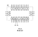
- FIG. 6 is a plan view of a major region of the wiring board according to Embodiment 5 including a semiconductor mounting region.
- second bump electrodes 13 b are provided at a region 50 that is covered with a solder resist film (not illustrated).
- a solder resist film not illustrated.
- FIG. 7 is a cross-sectional view of a semiconductor device according to Embodiment 6. Note here that the semiconductor device according to Embodiment 6 employs the above-stated wiring board 1 (see FIGS. 1A and B).
- the semiconductor device 6 includes a wiring board 1 and a semiconductor chip 60 mounted on first bump electrodes 13 a of the wiring board 1 . Since the semiconductor device 6 employs the wiring board 1 according to one embodiment of the present invention, the height of the first bump electrodes 13 a for bonding with the semiconductor chip 60 can be made uniform. With this configuration, the reliability of the electric connection between the semiconductor chip 60 and the first bump electrodes 13 a can be enhanced.
- reference numeral 61 denotes an electrode pad of the semiconductor chip 60
- 62 denotes a solder resist film
- 63 denotes a surface protective film that protects a surface of the semiconductor chip 60
- 64 denotes an encapsulation resin for protection.
- second bump electrodes are provided for adjusting a variation in height of bump electrodes for bonding (first bump electrodes). Therefore, a semiconductor chip and the first bump electrodes can be bonded reliably. Since the semiconductor device of the present invention employs the above-stated wiring board of the present invention, the reliability of the electric connection between a semiconductor chip and the first bump electrodes can be enhanced.
Abstract
Description
Claims (9)
Applications Claiming Priority (2)
| Application Number | Priority Date | Filing Date | Title |
|---|---|---|---|
| JP2006-110023 | 2006-04-12 | ||
| JP2006110023A JP4773864B2 (en) | 2006-04-12 | 2006-04-12 | Wiring board, semiconductor device using the same, and manufacturing method of wiring board |
Publications (2)
| Publication Number | Publication Date |
|---|---|
| US20070241462A1 US20070241462A1 (en) | 2007-10-18 |
| US7508073B2 true US7508073B2 (en) | 2009-03-24 |
Family
ID=38604084
Family Applications (1)
| Application Number | Title | Priority Date | Filing Date |
|---|---|---|---|
| US11/733,566 Active US7508073B2 (en) | 2006-04-12 | 2007-04-10 | Wiring board, semiconductor device using the same, and method for manufacturing wiring board |
Country Status (3)
| Country | Link |
|---|---|
| US (1) | US7508073B2 (en) |
| JP (1) | JP4773864B2 (en) |
| CN (1) | CN101055862A (en) |
Cited By (4)
| Publication number | Priority date | Publication date | Assignee | Title |
|---|---|---|---|---|
| US20130269987A1 (en) * | 2012-04-11 | 2013-10-17 | Johnson Electric S.A | Electrical component |
| US8633588B2 (en) * | 2011-12-21 | 2014-01-21 | Mediatek Inc. | Semiconductor package |
| US9633936B2 (en) * | 2012-03-27 | 2017-04-25 | Mediatek Inc. | Semiconductor package |
| US9659893B2 (en) | 2011-12-21 | 2017-05-23 | Mediatek Inc. | Semiconductor package |
Families Citing this family (3)
| Publication number | Priority date | Publication date | Assignee | Title |
|---|---|---|---|---|
| KR101842065B1 (en) * | 2011-07-21 | 2018-03-27 | 삼성디스플레이 주식회사 | Flexible circuit board |
| TWI514530B (en) * | 2013-08-28 | 2015-12-21 | Via Tech Inc | Circuit substrate, semiconductor package and process for fabricating a circuit substrate |
| CN104216149B (en) * | 2014-09-30 | 2017-03-22 | 南京中电熊猫液晶显示科技有限公司 | Liquid crystal display panel with repair wire structure |
Citations (6)
| Publication number | Priority date | Publication date | Assignee | Title |
|---|---|---|---|---|
| US6483190B1 (en) * | 1999-10-20 | 2002-11-19 | Fujitsu Limited | Semiconductor chip element, semiconductor chip element mounting structure, semiconductor chip element mounting device and mounting method |
| US6710458B2 (en) * | 2000-10-13 | 2004-03-23 | Sharp Kabushiki Kaisha | Tape for chip on film and semiconductor therewith |
| US20040212969A1 (en) | 2003-04-28 | 2004-10-28 | Matsushita Electric Industrial Co., Ltd. | Circuit board and method for manufacturing the same and semiconductor device and method for manufacturing the same |
| US6967394B2 (en) * | 2003-03-25 | 2005-11-22 | Oki Electric Industry Co., Ltd. | Multi-chip package |
| US20050272182A1 (en) * | 2000-09-29 | 2005-12-08 | Tessera, Inc. | Methods of making microelectronic packages |
| US7002250B2 (en) * | 2000-12-25 | 2006-02-21 | Renesas Technology Corp. | Semiconductor module |
Family Cites Families (7)
| Publication number | Priority date | Publication date | Assignee | Title |
|---|---|---|---|---|
| JPH0618226B2 (en) * | 1989-01-09 | 1994-03-09 | 株式会社ソニックス | Bumped film carrier and method of manufacturing the same |
| JP2894254B2 (en) * | 1995-09-20 | 1999-05-24 | ソニー株式会社 | Semiconductor package manufacturing method |
| WO1998018163A1 (en) * | 1996-10-22 | 1998-04-30 | Seiko Epson Corporation | Film carrier tape, tape carrier semiconductor device assembly, semiconductor device, its manufacturing method, package substrate, and electronic appliance |
| JPH11268324A (en) * | 1998-03-25 | 1999-10-05 | Brother Ind Ltd | Electrode substrate and manufacture thereof |
| JP3120848B2 (en) * | 1999-03-17 | 2000-12-25 | カシオ計算機株式会社 | Method for manufacturing semiconductor device |
| JP2000349196A (en) * | 1999-06-08 | 2000-12-15 | Sumitomo Metal Electronics Devices Inc | Electroplating method of electronic part and manufacture of the same |
| JP4506168B2 (en) * | 2003-12-24 | 2010-07-21 | カシオ計算機株式会社 | Semiconductor device and its mounting structure |
-
2006
- 2006-04-12 JP JP2006110023A patent/JP4773864B2/en not_active Expired - Fee Related
-
2007
- 2007-04-10 US US11/733,566 patent/US7508073B2/en active Active
- 2007-04-12 CN CNA2007100970347A patent/CN101055862A/en active Pending
Patent Citations (8)
| Publication number | Priority date | Publication date | Assignee | Title |
|---|---|---|---|---|
| US6483190B1 (en) * | 1999-10-20 | 2002-11-19 | Fujitsu Limited | Semiconductor chip element, semiconductor chip element mounting structure, semiconductor chip element mounting device and mounting method |
| US7436062B2 (en) * | 1999-10-20 | 2008-10-14 | Fujitsu Limited | Semiconductor chip element, semiconductor chip element mounting structure, semiconductor chip element mounting device and mounting method |
| US20050272182A1 (en) * | 2000-09-29 | 2005-12-08 | Tessera, Inc. | Methods of making microelectronic packages |
| US6710458B2 (en) * | 2000-10-13 | 2004-03-23 | Sharp Kabushiki Kaisha | Tape for chip on film and semiconductor therewith |
| US7002250B2 (en) * | 2000-12-25 | 2006-02-21 | Renesas Technology Corp. | Semiconductor module |
| US6967394B2 (en) * | 2003-03-25 | 2005-11-22 | Oki Electric Industry Co., Ltd. | Multi-chip package |
| US20040212969A1 (en) | 2003-04-28 | 2004-10-28 | Matsushita Electric Industrial Co., Ltd. | Circuit board and method for manufacturing the same and semiconductor device and method for manufacturing the same |
| JP2004327936A (en) | 2003-04-28 | 2004-11-18 | Matsushita Electric Ind Co Ltd | Wiring board, its manufacturing process, semiconductor device, and its manufacturing process |
Cited By (8)
| Publication number | Priority date | Publication date | Assignee | Title |
|---|---|---|---|---|
| US8633588B2 (en) * | 2011-12-21 | 2014-01-21 | Mediatek Inc. | Semiconductor package |
| US9142526B2 (en) | 2011-12-21 | 2015-09-22 | Mediatek Inc. | Semiconductor package with solder resist capped trace to prevent underfill delamination |
| US9640505B2 (en) | 2011-12-21 | 2017-05-02 | Mediatek Inc. | Semiconductor package with trace covered by solder resist |
| US9659893B2 (en) | 2011-12-21 | 2017-05-23 | Mediatek Inc. | Semiconductor package |
| US9633936B2 (en) * | 2012-03-27 | 2017-04-25 | Mediatek Inc. | Semiconductor package |
| US10553526B2 (en) | 2012-03-27 | 2020-02-04 | Mediatek Inc. | Semiconductor package |
| US20130269987A1 (en) * | 2012-04-11 | 2013-10-17 | Johnson Electric S.A | Electrical component |
| US9131617B2 (en) * | 2012-04-11 | 2015-09-08 | Johnson Electric S.A. | Electrical component |
Also Published As
| Publication number | Publication date |
|---|---|
| US20070241462A1 (en) | 2007-10-18 |
| CN101055862A (en) | 2007-10-17 |
| JP4773864B2 (en) | 2011-09-14 |
| JP2007287743A (en) | 2007-11-01 |
Similar Documents
| Publication | Publication Date | Title |
|---|---|---|
| US6593648B2 (en) | Semiconductor device and method of making the same, circuit board and electronic equipment | |
| US7294532B2 (en) | Method for manufacturing semiconductor device | |
| CN100517680C (en) | Wiring board, semiconductor device and display module | |
| US7087987B2 (en) | Tape circuit substrate and semiconductor chip package using the same | |
| US7508073B2 (en) | Wiring board, semiconductor device using the same, and method for manufacturing wiring board | |
| JP2004343030A (en) | Wiring circuit board, manufacturing method thereof, circuit module provided with this wiring circuit board | |
| US20210225755A1 (en) | Semiconductor device and method for manufacturing the same | |
| US7439611B2 (en) | Circuit board with auxiliary wiring configuration to suppress breakage during bonding process | |
| US7379307B2 (en) | Wiring board and method for manufacturing the same, and semiconductor device | |
| US7183660B2 (en) | Tape circuit substrate and semicondutor chip package using the same | |
| JP3000975B2 (en) | Semiconductor element mounting structure | |
| US6403895B1 (en) | Wiring substance and semiconductor | |
| KR20090026891A (en) | Wiring substrate, tape package having the same, display device having the same, method of manufacturing the same, method of manufacturing a tape package having the same and method of manufacturing a display device having the same | |
| KR20090084706A (en) | Printed circuit board and method of manufacturing the same | |
| TW201316464A (en) | Circuit board, fabricating method thereof and package structure | |
| KR20010033602A (en) | Semiconductor device and method of production thereof and semiconductor mounting structure and method | |
| US10178768B2 (en) | Mounting substrate, method for manufacturing a mounting substrate, and mounted structure including an electronic component | |
| KR100196119B1 (en) | Semiconductor device and manufacturing method thereof and electron device | |
| KR20000028840A (en) | Process for manufacturing semiconductor device using film substrate | |
| KR20190045037A (en) | Film for package substrate, semiconductor package, display device and methods of fabricating the same | |
| JP4973513B2 (en) | Tape carrier for semiconductor device, method for manufacturing tape carrier for semiconductor device, and semiconductor device | |
| JP2005109377A (en) | Semiconductor device and manufacturing method therefor | |
| JP3383597B2 (en) | Method for manufacturing semiconductor device | |
| KR20230028009A (en) | Flexible printed circuit board, cof module and electronic device comprising the same | |
| JP2000332143A (en) | Semiconductor device |
Legal Events
| Date | Code | Title | Description |
|---|---|---|---|
| AS | Assignment |
Owner name: MATSUSHITA ELECTRIC INDUSTRIAL CO., LTD., JAPAN Free format text: ASSIGNMENT OF ASSIGNORS INTEREST;ASSIGNORS:NAKAMURA, YOSHIFUMI;SHIMOISHIZAKA, NOZOMI;REEL/FRAME:019888/0489 Effective date: 20070402 |
|
| AS | Assignment |
Owner name: PANASONIC CORPORATION, JAPAN Free format text: CHANGE OF NAME;ASSIGNOR:MATSUSHITA ELECTRIC INDUSTRIAL CO., LTD.;REEL/FRAME:021897/0606 Effective date: 20081001 Owner name: PANASONIC CORPORATION,JAPAN Free format text: CHANGE OF NAME;ASSIGNOR:MATSUSHITA ELECTRIC INDUSTRIAL CO., LTD.;REEL/FRAME:021897/0606 Effective date: 20081001 |
|
| FEPP | Fee payment procedure |
Free format text: PAYOR NUMBER ASSIGNED (ORIGINAL EVENT CODE: ASPN); ENTITY STATUS OF PATENT OWNER: LARGE ENTITY |
|
| STCF | Information on status: patent grant |
Free format text: PATENTED CASE |
|
| FPAY | Fee payment |
Year of fee payment: 4 |
|
| FEPP | Fee payment procedure |
Free format text: PAYOR NUMBER ASSIGNED (ORIGINAL EVENT CODE: ASPN); ENTITY STATUS OF PATENT OWNER: LARGE ENTITY Free format text: PAYER NUMBER DE-ASSIGNED (ORIGINAL EVENT CODE: RMPN); ENTITY STATUS OF PATENT OWNER: LARGE ENTITY |
|
| FPAY | Fee payment |
Year of fee payment: 8 |
|
| AS | Assignment |
Owner name: PANASONIC SEMICONDUCTOR SOLUTIONS CO., LTD., JAPAN Free format text: ASSIGNMENT OF ASSIGNORS INTEREST;ASSIGNOR:PANASONIC CORPORATION;REEL/FRAME:052755/0917 Effective date: 20200521 |
|
| MAFP | Maintenance fee payment |
Free format text: PAYMENT OF MAINTENANCE FEE, 12TH YEAR, LARGE ENTITY (ORIGINAL EVENT CODE: M1553); ENTITY STATUS OF PATENT OWNER: LARGE ENTITY Year of fee payment: 12 |