US7518469B2 - Multi-band high-frequency circuit, multi-band high-frequency circuit component and multi-band communication apparatus using same - Google Patents

Multi-band high-frequency circuit, multi-band high-frequency circuit component and multi-band communication apparatus using same Download PDF

Info

Publication number
US7518469B2
US7518469B2 US10/596,372 US59637204A US7518469B2 US 7518469 B2 US7518469 B2 US 7518469B2 US 59637204 A US59637204 A US 59637204A US 7518469 B2 US7518469 B2 US 7518469B2
Authority
US
United States
Prior art keywords
circuit
frequency
band
diplexer
receiving
Prior art date
Legal status (The legal status is an assumption and is not a legal conclusion. Google has not performed a legal analysis and makes no representation as to the accuracy of the status listed.)
Active, expires
Application number
US10/596,372
Other versions
US20070075803A1 (en
Inventor
Shigeru Kemmochi
Keisuke Fukamachi
Kazuhiro Hagiwara
Masayuki Uchida
Current Assignee (The listed assignees may be inaccurate. Google has not performed a legal analysis and makes no representation or warranty as to the accuracy of the list.)
Murata Manufacturing Co Ltd
Original Assignee
Hitachi Metals Ltd
Priority date (The priority date is an assumption and is not a legal conclusion. Google has not performed a legal analysis and makes no representation as to the accuracy of the date listed.)
Filing date
Publication date
Application filed by Hitachi Metals Ltd filed Critical Hitachi Metals Ltd
Assigned to HITACHI METALS, LTD. reassignment HITACHI METALS, LTD. ASSIGNMENT OF ASSIGNORS INTEREST (SEE DOCUMENT FOR DETAILS). Assignors: FUKAMACHI, KEISUKE, HAGIWARA, KAZUHIRO, KEMMOCHI, SHIGERU, UCHIDA, MASAYUKI
Publication of US20070075803A1 publication Critical patent/US20070075803A1/en
Application granted granted Critical
Publication of US7518469B2 publication Critical patent/US7518469B2/en
Assigned to HITACHI METALS, LTD. reassignment HITACHI METALS, LTD. CHANGE OF ADDRESS Assignors: HITACHI METALS, LTD.
Assigned to MURATA MANUFACTURING CO., LTD. reassignment MURATA MANUFACTURING CO., LTD. ASSIGNMENT OF ASSIGNORS INTEREST (SEE DOCUMENT FOR DETAILS). Assignors: HITACHI METALS, LTD.
Active legal-status Critical Current
Adjusted expiration legal-status Critical

Links

Images

Classifications

    • HELECTRICITY
    • H04ELECTRIC COMMUNICATION TECHNIQUE
    • H04BTRANSMISSION
    • H04B1/00Details of transmission systems, not covered by a single one of groups H04B3/00 - H04B13/00; Details of transmission systems not characterised by the medium used for transmission
    • H04B1/005Details of transmission systems, not covered by a single one of groups H04B3/00 - H04B13/00; Details of transmission systems not characterised by the medium used for transmission adapting radio receivers, transmitters andtransceivers for operation on two or more bands, i.e. frequency ranges
    • H04B1/0053Details of transmission systems, not covered by a single one of groups H04B3/00 - H04B13/00; Details of transmission systems not characterised by the medium used for transmission adapting radio receivers, transmitters andtransceivers for operation on two or more bands, i.e. frequency ranges with common antenna for more than one band
    • H04B1/0057Details of transmission systems, not covered by a single one of groups H04B3/00 - H04B13/00; Details of transmission systems not characterised by the medium used for transmission adapting radio receivers, transmitters andtransceivers for operation on two or more bands, i.e. frequency ranges with common antenna for more than one band using diplexing or multiplexing filters for selecting the desired band
    • HELECTRICITY
    • H04ELECTRIC COMMUNICATION TECHNIQUE
    • H04BTRANSMISSION
    • H04B1/00Details of transmission systems, not covered by a single one of groups H04B3/00 - H04B13/00; Details of transmission systems not characterised by the medium used for transmission
    • H04B1/38Transceivers, i.e. devices in which transmitter and receiver form a structural unit and in which at least one part is used for functions of transmitting and receiving
    • H04B1/40Circuits
    • H04B1/44Transmit/receive switching

Definitions

  • the present invention relates to a wireless communication apparatus for performing wireless transmission between electronic or electric equipments, particularly to a multi-band high-frequency circuit and a multi-band high-frequency circuit component commonly usable for at least two communication systems and capable of conducting diversity receiving, and a multi-band communication apparatus comprising such a multi-band high-frequency circuit component.
  • WLAN wireless LAN
  • PCs personal computers
  • PC peripherals such as printers, hard disk drives, broadband rooters, etc.
  • electronic appliances such as facsimiles, refrigerators, standard-definition televisions (SDTVs), high-definition televisions (HDTVs), digital cameras, digital video recorders, cell phones, etc.; and as signal-transmitting means in place of wires in automobiles and aircrafts, and wireless data transmission is conducted among these electronic or electric appliances.
  • SDTVs standard-definition televisions
  • HDTVs high-definition televisions
  • digital cameras digital video recorders
  • cell phones cell phones
  • IEEE802.11a is adapted to high-speed data communications of 54 Mbps at maximum in a frequency band of 5 GHz, using an OFDM (orthogonal frequency division multiples) modulation system.
  • IEEE802.11h is the standard for making IEEE802.11a usable in Europe.
  • IEEE802.11b is adapted to high-speed communications of 5.5 Mbps and 11 Mbps in an industrial, scientific and medical (ISM) band of 2.4 GHz that can be freely used without wireless license, using a direct sequence spread spectrum (DSSS) system.
  • ISM industrial, scientific and medical
  • DSSS direct sequence spread spectrum
  • IEEE802.11g is adapted to high-speed data communications of 54 Mbps at maximum in a 2.4-GHz band like IEEE802.11b, using the OFDM (orthogonal frequency division multiples) modulation system.
  • IEEE802.11a and IEEE802.11h as a first communication system
  • IEEE802.11b and IEEE802.11g as a second communication system
  • This multi-band communication apparatus comprises two dual-band antennas capable of transmitting and receiving in two communication systems having different communication frequency bands (IEEE802.11a, IEEE802.11b), two transmitting/receiving means for modulating transmission data and demodulating receiving data in each communication system, pluralities of switch means for connecting the antennas to the transmitting/receiving means, and switch control means for controlling the switch means, so that it can perform diversity receiving (see FIG. 33 ).
  • IEEE802.11a, IEEE802.11b two transmitting/receiving means for modulating transmission data and demodulating receiving data in each communication system
  • pluralities of switch means for connecting the antennas to the transmitting/receiving means
  • switch control means for controlling the switch means, so that it can perform diversity receiving (see FIG. 33 ).
  • JP2002-033714A describes a multi-band communication apparatus using one multi-band antenna.
  • This multi-band communication apparatus comprises a 2.4-GHz-band, front-end circuit and a 5-GHz-band, front-end circuit each comprising a switch circuit, amplifiers, a mixer, etc., a switch circuit SW 1 for selectively connecting one of them to a common multi-band antenna, switch circuits SW 2 , SW 3 for switching transmitting/receiving circuits, and a switch circuit SW 4 connected to an intermediate-frequency filter BPF (see FIG. 34 ).
  • CSMA carrier sense multiple access
  • the antenna ANT 1 is connected to a receiving terminal Rx of the transmitting/receiving means of 802.11a, and the antenna ANT 2 is connected to a receiving terminal Rx of the transmitting/receiving means of 802.11b, by six single-pole, double-throw (SPDT) switch means (SW 1 -SW 6 ).
  • the transmitting/receiving means of 802.11a is scanned in a 5-GHz band, and the transmitting/receiving means of 802.11b is scanned in a 2.4-GHz band, to sense all receivable vacant channels.
  • the next step is to compare a receiving signal in a 5-GHz band received by the dual-band antenna ANT 1 with a receiving signal in a 2.4-GHz band received by the dual-band antenna ANT 2 , and select one of the two communication systems by which a more desired signal is received, as an active communication system.
  • the other antenna is connected to the transmitting/receiving means of the selected communication system to perform receiving without changing the receiving channel.
  • the receiving signals from two antennas are compared, and an antenna capable of performing better receiving is selected as an active antenna to conduct diversity receiving.
  • receiving signals in 2.4-GHz and 5-GHz bands are scanned by one dual-band antenna ANT 1 to sense all receivable vacant channels, and a channel of a desired communication system is selected.
  • the selection of communication system channels based on the comparison results of receiving signals obtained from different antennas or one antenna connected to each communication system is under unnegligible influence by disturbances such as noises from other communication systems and electronic equipments, phasing, etc., resulting in the likelihood that a communication system channel to be selected is erroneously sensed as busy, and that a communication system in which a receiving signal has the largest amplitude is not selected.
  • TPC transmission power control
  • a coupling circuit for instance, a directional coupler
  • a coupling circuit should be connected between the transmitting/receiving means of IEEE802.11a and the switch circuit SW 3 , and between the transmitting/receiving means of IEEE802.11b and the switch circuit SW 4 , to input a detection signal from the directional coupler to a detection circuit, thereby controlling an output signal based on the resultant detection voltage.
  • this method needs directional couplers, detection diodes and smoothing circuits in both 2.4-GHz band and 5-GHz band.
  • an analog switch for selecting detection voltage terminals in a 2.4-GHz band and a 5-GHz band is also needed. This increases the number of parts, resulting in difficulty in the miniaturization of communication apparatuses.
  • High-frequency circuits for WLAN also need filter circuits for removing unnecessary frequency components contained in transmission signals and receiving signals, in addition to switch circuits for switching diversity switches, transmitting circuits and receiving circuits. Further, balanced-to-unbalanced converters for converting balanced signals to unbalanced signals, and impedance-converting circuits are needed.
  • the first object of the present invention is to provide a multi-band high-frequency circuit commonly usable in at least two communication systems, and capable of selecting the most desirable wireless communication channel substantially without influence by noises, phasing, etc., and further capable of performing diversity receiving.
  • the second object of the present invention is to provide a multi-band high-frequency circuit capable of switching the connection of multi-band antennas to transmitting circuits and receiving circuits with a few switch means, which comprises a coupling circuit, a filter circuit, a balanced-to-unbalanced converter and an impedance-converting circuit with small numbers of parts.
  • the third object of the present invention is to provide a multi-band high-frequency circuit component comprising the above multi-band high-frequency circuit in a small three-dimensional laminate structure.
  • the fourth object of the present invention is to provide a multi-band communication apparatus comprising a transmitting/receiving means for modulating transmission data and demodulating receiving data in each communication system, and a switch circuit controller for controlling the switching of the high-frequency switches.
  • the multi-band high-frequency circuit for performing wireless communications among pluralities of communication systems having different communication frequencies comprises a high-frequency switch circuit comprising switching elements for switching the connection of pluralities of multi-band antennas to transmitting circuits and receiving circuits; a first diplexer circuit disposed between the high-frequency switch circuit and transmitting circuits for branching a high-frequency signal into frequency bands of the communication systems; a second diplexer circuit disposed between the high-frequency switch circuit and receiving circuits for branching a high-frequency signal into frequency bands of the communication systems; the first and second diplexer circuits each comprising a lower-frequency filter circuit and a higher-frequency filter circuit, a bandpass filter circuit being used as the lower-frequency filter circuit in the second diplexer circuit, or disposed between the lower-frequency filter circuit in the second diplexer circuit and the receiving circuit; the high-frequency switch circuit comprising first to fourth ports, the first port being connected to a first multi-band antenna, the second port being connected to a second multi-band antenna, the
  • the multi-band high-frequency circuit for performing wireless communications among pluralities of communication systems having different communication frequencies comprises a high-frequency switch circuit comprising switching elements for switching the connection of one multi-band antenna to transmitting circuits and receiving circuits; a first diplexer circuit disposed between the high-frequency switch circuit and the transmitting circuits for branching a high-frequency signal into frequency bands of the communication systems; a second diplexer circuit disposed between the high-frequency switch circuit and the receiving circuits for branching a high-frequency signal into frequency bands of the communication systems; the first and second diplexer circuits each comprising a lower-frequency filter circuit and a higher-frequency filter circuit, a bandpass filter circuit being used as the lower-frequency filter circuit in the second diplexer circuit, or disposed between the lower-frequency filter circuit in the second diplexer circuit and the receiving circuit; the high-frequency switch circuit comprising first to third ports, the first port being connected to a first multi-band antenna via a matching circuit, the second port being connected to the first diplexer
  • the bandpass filter circuit has, for instance, a passband of 2.4 GHz to 2.5 GHz, off-band high-frequency signals being attenuated to remove noises, so that the high-frequency circuit is resistant to their influence.
  • a coupling circuit for taking part of a transmission power in pluralities of communication systems may be disposed between the high-frequency switch circuit and the first diplexer circuit.
  • the coupling circuit is preferably constituted by a coupling capacitor, comprising a matching circuit disposed between the coupling circuit and a detection circuit.
  • the coupling circuit is preferably constituted by a directional coupler comprising a main line and a sub-line, comprising a matching circuit between one end of the sub-line and a detection circuit.
  • Each of the first and second diplexer circuits is constituted by parallel-connected lower-frequency filter circuit and higher-frequency filter circuit with one end as a common port, the lower-frequency filter circuit being a filter circuit permitting a 2.4-GHz-band, high-frequency signal to pass but attenuating a 5-GHz-band, high-frequency signal, and the higher-frequency filter being a filter circuit permitting a 5-GHz-band, high-frequency signal to pass but attenuating a 2.4-GHz-band transmission signal.
  • the lower-frequency filter circuit in the second diplexer circuit is preferably constituted by a phase circuit and a bandpass filter circuit having a 2.4-GHz passband, the phase circuit controlling the impedance of the bandpass filter circuit in a band of 5 GHz to high impedance when viewed from the high-frequency switch circuit.
  • the lower-frequency filter circuit is a lowpass filter circuit, a combination of a highpass filter circuit and a lowpass filter circuit, or a bandpass filter circuit
  • the higher-frequency filter circuit is preferably a highpass filter circuit or a bandpass filter circuit.
  • the multi-band high-frequency circuit comprises a first balanced-to-unbalanced converter disposed between the lower-frequency filter circuit in the second diplexer circuit and the receiving circuit, and a second balanced-to-unbalanced converter disposed between the higher-frequency filter circuit in the second diplexer circuit and the receiving circuit.
  • the multi-band high-frequency circuit comprises a transmitting/receiving means for modulating transmission data and demodulating receiving data in each communication system, and a switch circuit controller for controlling the switching of the high-frequency switch.
  • the multi-band high-frequency circuit component of the present invention comprises the above multi-band high-frequency circuit, a laminate of substrates having electrode patterns and elements mounted onto the laminate, at least part of inductance elements and capacitance elements being constituted by the electrode patterns, and at least the switching elements being mounted onto the laminate, among circuit elements constituting the high-frequency circuit.
  • the multi-band communication apparatus of the present invention comprises the multi-band high-frequency circuit or the multi-band high-frequency circuit component.
  • the multi-band high-frequency circuit of the present invention can select the most suitable channels substantially without influence by noises, phasing, etc. in data communications by WLAN, and perform diversity receiving. It can also switch the connection of multi-band antennas and transmitting/receiving circuits while suppressing power consumption with few numbers of switch means.
  • the high-frequency circuit of the present invention can be constructed in the form of a high-frequency circuit component having a small three-dimensional laminate structure. Further, it is possible to provide a multi-band communication apparatus with a transmitting/receiving means for modulating transmission data and demodulating receiving data in each communication system, and a switch circuit controller for controlling the switching of the high-frequency switch.
  • FIG. 1 is a block diagram showing the circuit of the multi-band communication apparatus according to one embodiment of the present invention.
  • FIG. 2 is a block diagram showing the multi-band high-frequency circuit according to one embodiment of the present invention.
  • FIG. 3 is a view showing the equivalent circuit of the multi-band high-frequency circuit according to one embodiment of the present invention.
  • FIG. 4 is a view showing the equivalent circuit of one example of DPDT switches used in the present invention.
  • FIG. 5 is a view showing the equivalent circuit of another example of DPDT switches used in the present invention.
  • FIG. 6 is a view showing the equivalent circuit of a further example of DPDT switches used in the present invention.
  • FIG. 7 is a view showing the equivalent circuit of a still further example of DPDT switches used in the present invention.
  • FIG. 8 is a view showing the equivalent circuit of one example of diplexer circuits used in the present invention.
  • FIG. 9 is a view showing the equivalent circuit of another example of diplexer circuits used in the present invention.
  • FIG. 10 is a view showing the equivalent circuit of one example of filter circuits used in the present invention.
  • FIG. 11 is a view showing the equivalent circuit of another example of filter circuits used in the present invention.
  • FIG. 12 is a view showing the equivalent of a further example of filter circuits used in the present invention.
  • FIG. 13 is a view showing the equivalent circuit of a still further example of filter circuits used in the present invention.
  • FIG. 14 is a view showing the equivalent circuit of one example of balanced-to-unbalanced circuits used in the present invention.
  • FIG. 15 is a view showing the equivalent circuit of another example of balanced-to-unbalanced circuits used in the present invention.
  • FIG. 16 is a view showing the equivalent circuit of a further example of balanced-to-unbalanced circuits used in the present invention.
  • FIG. 17 is a block diagram showing a multi-band high-frequency circuit according to another embodiment of the present invention.
  • FIG. 18 is a view showing the equivalent circuit of one example of SPDT switches used in the present invention.
  • FIG. 19 is a view showing the equivalent circuit of another example of SPDT switches used in the present invention.
  • FIG. 20 is a view showing the equivalent circuit of a further example of SPDT switches used in the present invention.
  • FIG. 21 is a block diagram showing a multi-band high-frequency circuit according to a further embodiment of the present invention.
  • FIG. 22 is a view showing the equivalent circuit of one example of SPST switches used in the present invention.
  • FIG. 23 is a view showing the equivalent circuit of another example of SPST switches used in the present invention.
  • FIG. 24 is a view showing the equivalent circuit of a further example of SPST switches used in the present invention.
  • FIG. 25 is a view showing the equivalent circuit of a still further example of SPST switches used in the present invention.
  • FIG. 26 is a perspective view showing a multi-band high-frequency circuit component according to one embodiment of the present invention.
  • FIG. 27 is an exploded perspective view showing part of laminate substrates constituting the multi-band high-frequency circuit component of the present invention.
  • FIG. 28 is an exploded perspective view showing the remainders of laminate substrates constituting the multi-band high-frequency circuit component of the present invention.
  • FIG. 29 is a view showing the equivalent circuit of a multi-band high-frequency circuit according to a still further embodiment of the present invention.
  • FIG. 30 is a block diagram showing a multi-band high-frequency circuit according to a still further embodiment of the present invention.
  • FIG. 31 is a view showing the equivalent circuit of a multi-band high-frequency circuit according to a still further embodiment of the present invention.
  • FIG. 32 is a view showing the equivalent circuit of a multi-band high-frequency circuit according to a still further embodiment of the present invention.
  • FIG. 33 is a block diagram showing a conventional multi-band communication apparatus.
  • FIG. 34 is a block diagram showing another conventional multi-band communication apparatus.
  • FIG. 1 shows the circuit of the multi-band communication apparatus according to a preferred embodiment of the present invention.
  • This multi-band communication apparatus comprises two multi-band antennas ANT 1 , ANT 2 transmittable and receivable in a 2.4-GHz band and a 5-GHz-band; a high-frequency switch 1 or a high-frequency circuit 1 comprising pluralities of diplexer circuits for switching the connection of the multi-band antennas and the transmitting circuits and receiving circuits; a transmitting/receiving circuit RF-IC comprising a transmitting/receiving means of IEEE802.11a and a transmitting/receiving means of IEEE802.11b for modulating transmission data and demodulating receiving data in each communication system, a switch circuit controller for controlling the switching of the high-frequency switch, and amplifiers for receiving signals; balanced-to-unbalanced converters 53 , 54 for converting balanced signals to unbalanced signals; and amplifiers PA 1 , PA 2 for transmission signals connected to the balanced-to-unbalanced
  • the first communication system is IEEE802.11a
  • the second communication system is IEEE802.11b
  • the present invention is not particularly restricted thereto.
  • IEEE802.11h uses the same frequency band as IEEE802.11a
  • IEEE802.11g uses the same frequency band as IEEE802.11b as described above
  • each circuit may be used in each communication system.
  • a transmitting/receiving means capable of handling each of them is necessary, because they need different modulation systems.
  • FIG. 2 shows one example of the high-frequency circuit 1
  • FIG. 3 shows the equivalent circuit of the high-frequency circuit 1
  • the multi-band high-frequency circuit of the present invention (high-frequency circuit 1 ) comprises a high-frequency switch circuit 10 , and first and second diplexer circuits 20 , 25 connected thereto as basic components.
  • the multi-band high-frequency circuit in this embodiment comprises a double-pole, double-throw (DPDT) high-frequency switch circuit 10 having four ports, which is connected to pluralities of multi-band antennas and pluralities of diplexer circuits.
  • DPDT double-pole, double-throw
  • the high-frequency switch circuit 10 has a first port 10 a connected to a first multi-band antenna ANT 1 via a matching circuit constituted by a coupling capacitor C 1 capable of functioning as a DC-cutting capacitor, a second port 10 b connected to a second multi-band antenna ANT 2 via a matching circuit constituted by a coupling capacitor C 2 , a third port 10 c connected to a first diplexer circuit 20 for branching transmission signals, and a fourth port 10 d connected to a second diplexer circuit 25 for branching receiving signals.
  • the first diplexer circuit 20 has a third port 20 c connected to a filter circuit 60
  • the second diplexer circuit 25 has a second port 25 b connected to a filter circuit 30 and a balanced-to-unbalanced converter 50
  • a third port 25 c connected to a filter circuit 40 and a balanced-to-unbalanced converter 55 .
  • the high-frequency switch circuit 10 is mainly constituted by switching elements such as field-effect transistors (FETs), diodes, etc., and may comprise inductance elements and capacitance elements, if necessary.
  • FETs field-effect transistors
  • FIG. 4 One structural example of the high-frequency switch circuit 10 is shown in FIG. 4 .
  • This high-frequency switch circuit 10 comprises four field-effect transistors series-connected to four annually disposed signal paths, and DC-cutting capacitors C series-connected to a third port 10 c and a fourth port 10 d among four signal paths. Because of small numbers of switching elements disposed in the high-frequency signal paths, little loss is generated by the switching elements.
  • Ports 10a Ports 10a Ports 10b Ports 10b Mode V1 V2 and 10c and 10d and 10c and 10d 1 High Low Connected Dis- Dis- Connected connected connected connected 2 Low High Dis- Connected Connected Dis- connected connected
  • the field-effect transistors FET 1 and FET 4 are in an ON state, while the field-effect transistors FET 2 and FET 3 are in an OFF state. Accordingly, a high-frequency signal input through the port 10 c (on the side of the first diplexer circuit) of the high-frequency switch circuit 10 passes through the field-effect transistor FET 1 in an ON state, and transmitted to the port 10 a (on the side of the first multi-band antenna). Because the field-effect transistor FET 3 is in an OFF state at this time, its isolation characteristics substantially prevent the high-frequency signal from leaking to the port 10 b (on the side of the second multi-band antenna). Also, because the field-effect transistor FET 2 is in an OFF state, substantially no high-frequency signal leaks to the port 10 d (on the side of the second diplexer circuit).
  • a high-frequency signal input through the port 10 b (on the side of the second multi-band antenna) of the high-frequency switch circuit 10 passes through the field-effect transistor FET 4 in an ON state, and transmitted to the port 10 d (on the side of the second diplexer circuit).
  • the field-effect transistor FET 2 is in an OFF state, the high-frequency signal does not substantially leak to the port 10 a (on the side of the first multi-band antenna).
  • the field-effect transistor FET 3 is also in an OFF state, substantially no high-frequency signal leaks to the port 10 c (on the side of the first diplexer circuit).
  • a high-frequency signal input through the port 10 c (on the side of the first diplexer circuit) of the high-frequency switch circuit 10 passes through the field-effect transistor FET 3 in an ON state, and transmitted to the port 10 b (on the side of the second multi-band antenna).
  • frequency scanning is first conducted before starting communications to sense a receivable frequency channel (carrier scanning).
  • the high-frequency switch circuit 10 is controlled, for instance, to the connection mode 1 shown in Table 1 by the switch circuit controller.
  • the second multi-band antenna ANT 2 is connected to the second diplexer circuit 25 , resulting in the connection of one multi-band antenna to the receiving circuits of two communication systems.
  • the second diplexer circuit 25 connected to the fourth port 10 d of the high-frequency switch circuit 10 is constituted by a combination of a lower-frequency filter circuit permitting a high-frequency signal in a 2.4-GHz band (IEEE802.11b) to pass but attenuating a high-frequency signal in a 5-GHz band (802.11a), and a higher-frequency filter circuit permitting a high-frequency signal in a 5-GHz band (IEEE802.11a) to pass but attenuating a transmission signal in a 2.4-GHz band (IEEE802.11b).
  • the lower-frequency filter circuit is constituted by a lowpass filter circuit comprising inductance elements and capacitance elements, while the higher-frequency filter circuit is constituted by a highpass filter circuit.
  • a 2.4-GHz-band, high-frequency signal appears at the second port 25 b of the second diplexer circuit 25 , but not at the third port 25 c
  • a 5-GHz-band, high-frequency signal appears at the third port 25 c of the second diplexer circuit 2 , but not at the second port 25 b .
  • the 2.4-GHz-band, high-frequency signal is separated from the 5-GHz-band, high-frequency signal.
  • the high-frequency signal appearing at its second port 25 b with noise components removed by the bandpass filter circuit 30 is converted from an unbalanced signal to a balanced signal by the balanced-to-unbalanced converter 50 and input to the receiving circuit of IEEE802.11b. Also, the high-frequency signal appearing at the third port 25 c is input to the receiving circuit of 55 IEEE802.11a via a filter circuit 40 and a balanced-to-unbalanced converter.
  • scanning is performed in a 5-GHz band in the receiving circuit of IEEE802.11a, and in a 2.4-GHz band in the transmitting/receiving means of 802.11b, to sense all receivable channels.
  • the switch circuit 10 is controlled to a connection mode 2 by the switch circuit controller.
  • the first multi-band antenna ANT 1 is connected to the second diplexer circuit 25 on the receiving circuit side. Based on the resultant high-frequency signal, scanning is performed in a 5-GHz band in the receiving circuit of IEEE802.11a, and in a 2.4-GHz band in the transmitting/receiving means of IEEE802.11b, to sense all receivable channels.
  • the channel of a communication system to be activated is selected, and receiving signals received by the first and second dual-band antennas ANT 1 , ANT 2 are compared in amplitude to select a multi-band antenna to be connected to the transmitting/receiving circuit of the communication system.
  • the most suited communication system can be selected even with disturbance such as phasing, etc. to conduct diversity receiving. Also, by performing carrier sense by a receiving signal made free from noises by a filter circuit, the most suitable channel in the wireless communications can be selected. When it is detected in the carrier sense that all channels are being used (busy), the carrier sense is performed again after the lapse of a certain period of time.
  • the selected multi-band antenna is connected to the first diplexer circuit 20 via the third port 10 c of the high-frequency switch circuit 10 .
  • the first diplexer circuit 20 is constituted by a combination of a lower-frequency filter circuit permitting a high-frequency signal in a 2.4-GHz band (IEEE802.11b) to pass but attenuating a high-frequency signal in a 5-GHz band (IEEE802.11a), and a higher-frequency filter circuit permitting a high-frequency signal in a 5-GHz band (IEEE802.11a) to pass but attenuating a transmission signal in a 2.4-GHz band (IEEE802.11b).
  • the lower-frequency filter circuit is constituted by a lowpass filter circuit
  • the higher-frequency filter circuit is constituted by a highpass filter circuit.
  • a 2.4-GHz-band, high-frequency signal input from the transmitting circuit of IEEE802.11b to the second port 20 b of the first diplexer circuit 20 appears at the first port 20 a via the lower-frequency filter circuit, but not at the third port 20 c .
  • a 5-GHz-band, high-frequency signal input from the transmitting circuit of IEEE802.11a to the third port 20 c of the first diplexer circuit appears at the first port 20 a via the higher-frequency filter circuit, but not at the second port 20 b .
  • the 2.4-GHz-band, high-frequency signal and the 5-GHz-band, high-frequency signal can be branched. Incidentally, because high-frequency signals in a 2.4-GHz band and a 5-GHz band are taken from the same port, it may be called “synthesized.”
  • the high-frequency signal appearing at the first port 20 a is input to the third port 10 c of the switch circuit and radiated from the multi-band antenna.
  • the equivalent circuits of other switch circuits 10 are shown in FIGS. 5-7 .
  • These equivalent circuits comprise as main elements switching elements such as field-effect transistors FET, diodes D 1 -D 4 , etc., as well as proper inductance elements and capacitance elements. For instance, they may be constituted using two single-pole, double-throw (SPDT) switches.
  • SPDT single-pole, double-throw
  • the first and second diplexer circuits 20 , 25 are constituted by proper combinations of lowpass filter circuits, highpass filter circuits and bandpass filter circuits comprising inductance elements and capacitance elements.
  • the equivalent circuits of the diplexer circuits 20 , 25 are exemplified in FIGS. 8 and 9 .
  • Filter circuits 30 , 40 , 60 are also constituted by lowpass filter circuits, highpass filter circuits and/or bandpass filter circuits. These filter circuits are properly selected by the off-band attenuation of the diplexer circuits 20 , 25 .
  • Other equivalent circuits of the filter circuit 30 , 40 , 60 are exemplified in FIGS. 10-13 .
  • the balanced-to-unbalanced converters 50 , 55 are constituted by inductance elements and capacitance elements, and may have an impedance-converting function. Their equivalent circuits are exemplified in FIGS. 14-16 . Because the use of an unbalanced input-balanced output SAW filter can integrate filter circuits and balanced-to-unbalanced converters into one circuit element, the number of elements can be reduced, resulting in the cost reduction and miniaturization of the high-frequency circuit.
  • a SAW filter with different input impedance and output impedance may be used. In this case, it may have an impedance-converting function.
  • an FBAR filter may be used.
  • the multi-band high-frequency circuits comprising various diplexer circuits, filter circuits, balanced-to-unbalanced converters and/or switch circuits described above exhibit excellent function, like the multi-band high-frequency circuit shown in FIG. 3 .
  • an SPDT switch 12 as the high-frequency switch circuit 10 can provide a multi-band high-frequency circuit connected to one multi-band antenna as shown in the block diagram of FIG. 17 .
  • the switch circuit shown in FIGS. 18-20 may be properly used.
  • a single-pole, single-throw (SPST) switch circuit 11 is preferably disposed between the high-frequency switch circuit 10 and the second diplexer circuit 25 .
  • the SPST switch circuit 11 is constituted, for instance, by a switching element, an inductance element and a capacitance element as shown in FIGS. 22-25 , to control that a signal is shut when the port 10 c of the high-frequency switch circuit 10 is connected to the port 10 a or 10 b.
  • FIGS. 26-28 An example of the multi-band high-frequency circuit having the equivalent circuit shown in FIG. 3 formed in a laminate is shown in FIGS. 26-28 .
  • FIG. 26 shows the appearance of a multi-band high-frequency circuit component comprising first and second diplexer circuits 20 , 25 , filter circuits 30 , 40 , 60 , first and second balanced-unbalanced circuits 50 , 55 , etc. in and on a laminate.
  • FIGS. 27 and 28 show the structure of each layer in the laminate 100 constituting the high-frequency circuit component.
  • the laminate 100 is produced by laminating pluralities of ceramic green sheets as thick as 10-200 ⁇ m and made of, for instance, a dielectric ceramic sinterable at as low a temperature as 1000° C. or lower, each of which is provided with an electrode pattern formed by printing a conductive paste of Ag, Cu, etc., and integrally sintering them.
  • a lowermost green sheet 15 is covered with a ground electrode GND on its front surface, and provided with terminal electrodes for mounting to a circuit substrate on its rear surface.
  • the terminal electrodes comprise antenna ports ANT 1 , ANT 2 , transmission ports Tx 1 , Tx 2 for inputting unbalanced signals, receiving ports Rx 1 +, Rx 1 ⁇ , Rx 2 +, Rx 2 ⁇ for outputting balanced signals, ground ports GND, and switch circuit-controlling ports V 1 , V 2 , and these ports are connected to electrode patterns on green sheets above through via-holes (shown by black circles in the figure) formed in the green sheets.
  • the terminal electrodes in a land grid array (LGA), but may be in a ball grid array (BGA), etc.
  • Green sheets 1 - 14 are laminated on the green sheet 15 .
  • the first and second diplexer circuits 20 , 25 , the filter circuits 30 , 40 , 60 , and the balanced-to-unbalanced converters 50 , 55 are constituted by inductance elements formed by transmission lines, and capacitance elements formed by predetermined electrode patterns, which are properly connected through via-holes.
  • Matching circuits 80 , 85 disposed between the filter circuits 30 , 40 and the balanced-to-unbalanced converters 50 , 55 are formed by transmission lines having predetermined length.
  • the inductance elements and the capacitance elements may of course be mounted onto the laminate 100 as chip inductors and chip capacitors.
  • Each circuit is three-dimensionally formed in the laminate 100 , and electrode patterns constituting the circuits are disposed such that they are separated by the ground electrode GND or do not overlap in a lamination direction, to prevent unnecessary electromagnetic interference.
  • Transmission lines through which a 5-GHz-band, high-frequency signal passes are separate from the other electrode patterns by at least 50 ⁇ m, to prevent electromagnetic interference.
  • Dielectric materials may be, for instance, ceramics comprising Al, Si and Sr as main components, and Ti, Bi, Cu, Mn, Na, K, etc. as sub-components; ceramics comprising Al, Si and Sr as main components, Ca, and Pb, Na, K, etc. as sub-components; ceramics comprising Al, Mg, Si and Gd; or ceramics comprising Al, Si, Zr and Mg.
  • the dielectric materials have dielectric constants of about 5-15.
  • resins and resin/ceramic composite materials may be used.
  • electrode patterns may be formed by high-temperature-sinterable metal conductors such as tungsten, molybdenum, etc. on Al 2 O 3 -based dielectric substrates, by a high-temperature cofirable ceramic (HTCC) technology.
  • HTCC high-temperature cofirable ceramic
  • Pluralities of land electrodes are formed on a green sheet 1 , and DPDT switches (GaAs FETs), and coupling capacitors that cannot be formed in the laminate are mounted as chip parts onto the land electrodes.
  • the land electrodes are connected to connecting lines and circuit elements in the laminate through via-holes.
  • Bare switches are mounted onto the land electrodes, and the land electrodes may be sealed by resins or pipes.
  • Such multi-band high-frequency circuit components are suitably miniaturized.
  • RF-ICs or base-band ICs constituting the transmitting/receiving circuits may be integrated to the laminate.
  • FIG. 29 shows the equivalent circuit of another multi-band high-frequency circuit.
  • the feature of this multi-band high-frequency circuit is that the lower-frequency filter circuit in the second diplexer circuit 25 is constituted by a phase circuit Lfr 1 and a bandpass filter circuit 30 having a 2.4-GHz passband.
  • the phase circuit Lfr 1 properly adjust the phase of a high-frequency signal, so that when viewed from the high-frequency switch circuit, the bandpass filter circuit 30 has high impedance in a band of 5 GHz, thereby preventing a 5-GHz-band, high-frequency signal from leaking to the receiving circuit in a 2.4-GHz band.
  • the multi-band high-frequency circuit can be constituted by small numbers of circuit elements.
  • FIGS. 30-32 A multi-band high-frequency circuit in a further embodiment is shown in FIGS. 30-32 .
  • FIG. 30 shows a transmitting circuit in a multi-band high-frequency circuit comprising a coupling circuit.
  • a coupling circuit 150 adapted to pluralities of communication systems for getting part of transmission power is disposed between the high-frequency switch circuit 10 and the first diplexer circuit 20 in the multi-band high-frequency circuit in Embodiment 1.
  • part of output power is detected from a 2.4-GHz-band, high-frequency signal and a 5-GHz-band, high-frequency signal by the coupling circuit 150 and a detection circuit 300 comprising a detection diode (Schottky diode).
  • detection accuracy is increased by monitoring the output power near the antenna output terminal.
  • the coupling circuit 150 may be constituted, for instance, by a directional coupler or a coupling capacitor.
  • one coupling circuit is used in a 2.4-GHz band and a 5-GHz band.
  • the coupling circuit has a larger coupling degree in a 5-GHz band than in a 2.4-GHz band, with the difference as large as about 5 dB.
  • the coupling degree difference directly affects detection voltage, resulting in different detection voltage to the output power from the amplifier.
  • the impedance of the coupling circuit 150 and the impedance of the detection circuit 300 are matched in a 2.4-GHz band, so that large detection voltage can be obtained even in a 2.4-GHz band with a small coupling degree (detection voltage) difference.
  • the matching circuit is preferably constituted by a shunt inductor connected to the output port 150 c of the coupling circuit 150 , and a phase circuit connected between the coupling circuit 150 and the detection diode.
  • a shunt inductor connected to the output port 150 c of the coupling circuit 150
  • a phase circuit connected between the coupling circuit 150 and the detection diode.
  • FIG. 31 shows the equivalent circuit of a coupling circuit 150 in the multi-band high-frequency circuit comprising a directional coupler as the coupling circuit.
  • the directional coupler is constituted by a main line STL 1 , a sub-line STL 2 and a resistor R 1 , so that a transmission signal from the first diplexer circuit 20 is input to the input port 150 b of the directional coupler 150 and output from the output port 150 a .
  • the main line STL 1 and the sub-line STL 2 are electromagnetically coupled, so that part of the transmission signal is output to the coupling port 150 c.
  • the matching circuit 200 is constituted by a shunt inductor Lss and a phase circuit Lsi, and the constants of the shunt inductor Lss and the phase circuit Lsi are set such that the output impedance of the coupling port 150 c of the directional coupling circuit is matched with the input impedance of the detection circuit 300 in a 2.4-GHz band.
  • the shunt inductor Lss performs amplitude adjustment
  • the phase circuit Lsi performs phase matching.
  • the detection diode Dk has an anode connected to the matching circuit 200 , and a cathode connected to a voltage-smoothing circuit comprising shunt-connected capacitor Ck and resistor Rk.
  • a high-frequency signal from the coupling circuit 150 is input to the detection diode Dk, and only a high-frequency signal exceeding its forward voltage is transmitted to the cathode, converted to DC voltage by the smoothing circuit, and input as detection voltage to a comparison control means connected to the output side of the detection circuit 300 .
  • the comparison control means 400 is constituted by an operational amplifier, resistors, control transistors, etc., to compare an input reference signal and a detection signal supplied from the detection diode Dk to change the output power of the amplifier such that the level difference between the two signals becomes zero.
  • FIG. 32 shows a high-frequency circuit in which the coupling circuit portion shown in FIG. 31 is constituted by a coupling capacitor Cc 1 .
  • the coupling degree is higher by about 5 dB in a 2.4-GHz band than in a 5-GHz band, so that the detection voltage in a 2.4-GHz band can be increased by the matching circuit 200 to reduce the difference from that in a 5-GHz band.
  • the multi-band high-frequency circuit of the present invention can select the most suitable channel without being influenced by noises, phasing, etc. in data communications by WLAN, and perform diversity receiving.
  • the multi-band high-frequency circuit of the present invention can also switch the connection of multi-band antennas and transmitting circuits/receiving circuits while suppressing power consumption with few numbers of switch means.
  • a multi-band communication apparatus with a transmitting/receiving means for modulating transmission data and demodulating receiving data in each communication system, and a switch circuit controller for controlling the switching of the high-frequency switch.
  • the multi-band high-frequency circuit of the present invention having such features is suitable for personal computers, PC peripherals such as printers, hard disk drives, broadband rooters, etc.; electronic appliances such as facsimiles, refrigerators, standard-definition televisions, high-definition televisions, digital cameras, digital video recorders, cell phones, etc.; and signal-transmitting means in automobiles and aircrafts.

Abstract

A multi-band high-frequency circuit for performing wireless communications among pluralities of communication systems having different communication frequencies, comprising a high-frequency switch circuit comprising switching elements for switching the connection of pluralities of multi-band antennas to transmitting circuits and receiving circuits; a first diplexer circuit disposed between the high-frequency switch circuit and transmitting circuits for branching a high-frequency signal into frequency bands of the communication systems; a second diplexer circuit disposed between the high-frequency switch circuit and receiving circuits for branching a high-frequency signal into frequency bands of the communication systems; the first and second diplexer circuits each comprising a lower-frequency filter circuit and a higher-frequency filter circuit, a bandpass filter circuit being used as the lower-frequency filter circuit in the second diplexer circuit, or disposed between the lower-frequency filter circuit in the second diplexer circuit and the receiving circuit; the high-frequency switch circuit comprising first to fourth ports, the first port being connected to a first multi-band antenna, the second port being connected to a second multi-band antenna, the third port being connected to the first diplexer circuit, and the fourth port being connected to the second diplexer circuit; and the switching elements being controlled in an ON or OFF state to select a multi-band antenna for performing wireless communications and to switch the connection of the selected multi-band antenna to the transmitting circuit or the receiving circuit.

Description

FIELD OF THE INVENTION
The present invention relates to a wireless communication apparatus for performing wireless transmission between electronic or electric equipments, particularly to a multi-band high-frequency circuit and a multi-band high-frequency circuit component commonly usable for at least two communication systems and capable of conducting diversity receiving, and a multi-band communication apparatus comprising such a multi-band high-frequency circuit component.
BACKGROUND OF THE INVENTION
Data communications by wireless LAN (WLAN) typically according to the IEEE802.11 standards are now widely used. They are used in personal computers (PCs); PC peripherals such as printers, hard disk drives, broadband rooters, etc.; electronic appliances such as facsimiles, refrigerators, standard-definition televisions (SDTVs), high-definition televisions (HDTVs), digital cameras, digital video recorders, cell phones, etc.; and as signal-transmitting means in place of wires in automobiles and aircrafts, and wireless data transmission is conducted among these electronic or electric appliances.
There are now pluralities of standards of wireless LAN. For instance, IEEE802.11a is adapted to high-speed data communications of 54 Mbps at maximum in a frequency band of 5 GHz, using an OFDM (orthogonal frequency division multiples) modulation system. Incidentally, there is IEEE802.11h as the standard for making IEEE802.11a usable in Europe.
IEEE802.11b is adapted to high-speed communications of 5.5 Mbps and 11 Mbps in an industrial, scientific and medical (ISM) band of 2.4 GHz that can be freely used without wireless license, using a direct sequence spread spectrum (DSSS) system.
IEEE802.11g is adapted to high-speed data communications of 54 Mbps at maximum in a 2.4-GHz band like IEEE802.11b, using the OFDM (orthogonal frequency division multiples) modulation system.
Explanation will be made below using IEEE802.11a and IEEE802.11h as a first communication system, and IEEE802.11b and IEEE802.11g as a second communication system, if necessary.
A multi-band communication apparatus using such WLAN is described in JP2003-169008A. This multi-band communication apparatus comprises two dual-band antennas capable of transmitting and receiving in two communication systems having different communication frequency bands (IEEE802.11a, IEEE802.11b), two transmitting/receiving means for modulating transmission data and demodulating receiving data in each communication system, pluralities of switch means for connecting the antennas to the transmitting/receiving means, and switch control means for controlling the switch means, so that it can perform diversity receiving (see FIG. 33).
As another example, JP2002-033714A describes a multi-band communication apparatus using one multi-band antenna. This multi-band communication apparatus comprises a 2.4-GHz-band, front-end circuit and a 5-GHz-band, front-end circuit each comprising a switch circuit, amplifiers, a mixer, etc., a switch circuit SW1 for selectively connecting one of them to a common multi-band antenna, switch circuits SW2, SW3 for switching transmitting/receiving circuits, and a switch circuit SW4 connected to an intermediate-frequency filter BPF (see FIG. 34).
In multi-band communication apparatuses for WLAN, a carrier sense multiple access (CSMA:) system is adopted to scan the frequency to sense the receivable frequency channel (carrier) before starting communications.
In the multi-band communication apparatus of JP2003-169008A, to conduct this scanning operation, the antenna ANT1 is connected to a receiving terminal Rx of the transmitting/receiving means of 802.11a, and the antenna ANT2 is connected to a receiving terminal Rx of the transmitting/receiving means of 802.11b, by six single-pole, double-throw (SPDT) switch means (SW1-SW6). The transmitting/receiving means of 802.11a is scanned in a 5-GHz band, and the transmitting/receiving means of 802.11b is scanned in a 2.4-GHz band, to sense all receivable vacant channels.
The next step is to compare a receiving signal in a 5-GHz band received by the dual-band antenna ANT1 with a receiving signal in a 2.4-GHz band received by the dual-band antenna ANT2, and select one of the two communication systems by which a more desired signal is received, as an active communication system.
After this scanning operation, the other antenna is connected to the transmitting/receiving means of the selected communication system to perform receiving without changing the receiving channel. The receiving signals from two antennas are compared, and an antenna capable of performing better receiving is selected as an active antenna to conduct diversity receiving.
Also, in the multi-band communication apparatus of JP2002-033714A, receiving signals in 2.4-GHz and 5-GHz bands are scanned by one dual-band antenna ANT1 to sense all receivable vacant channels, and a channel of a desired communication system is selected.
As in the conventional multi-band communication apparatuses, the selection of communication system channels based on the comparison results of receiving signals obtained from different antennas or one antenna connected to each communication system is under unnegligible influence by disturbances such as noises from other communication systems and electronic equipments, phasing, etc., resulting in the likelihood that a communication system channel to be selected is erroneously sensed as busy, and that a communication system in which a receiving signal has the largest amplitude is not selected.
There are electromagnetic waves leaking from electronic ovens, noises from communication systems such as Bluetooth®, radio frequency identification (RFID), etc. particularly in a frequency band of 2.4 GHz, and there are communication systems of cell phones having relatively large transmission power, such as WCDMA (wide band code division multiple access), etc., in nearby frequency bands. These high-frequency signals interfere communications in the WLAN systems. However, the conventional multi-band communication apparatuses do not have any measure to cope with such noises, etc.
Also, because high-frequency signal paths should be switched by many switch means in the conventional multi-band communication apparatus, control becomes complicated depending on the number of switch means. Because the switch means have transmission loss to some extent, many switch means disposed in paths from antennas to transmitting/receiving means increase transmission loss according to their number. Particularly at the time of receiving, the quality of a high-frequency signal input through an antenna is disadvantageously deteriorated. In addition, because power consumed by switching means is not negligible in battery-driven equipments such as note PCs, cell phones, etc., it has been requested to constitute a multi-band high-frequency circuit with few numbers of switch means.
In IEEE802.11h, the function of dynamic frequency selection (DFS) or transmission power control (TPC) is newly required. The TPC function is to reduce power consumed for transmission to a minimum level when good communications can be made even at a suppressed transmission power, for instance, in a case where mobile terminals are close to a base.
Various circuit elements such as switch circuits, etc. disposed between the output port of a power amplifier and a multi-band antenna generate insertion loss. Because this insertion loss has frequency characteristics, output power from a multi-band antenna is not constant depending on frequency channels used by the multi-band high-frequency circuit, but variable depending on the channels used. Accordingly, it is necessary to precisely control output power from the amplifier.
For instance, to perform a TPC function in the multi-band communication apparatus of JP2003-169008A, a coupling circuit (for instance, a directional coupler) should be connected between the transmitting/receiving means of IEEE802.11a and the switch circuit SW3, and between the transmitting/receiving means of IEEE802.11b and the switch circuit SW4, to input a detection signal from the directional coupler to a detection circuit, thereby controlling an output signal based on the resultant detection voltage. However, this method needs directional couplers, detection diodes and smoothing circuits in both 2.4-GHz band and 5-GHz band. Further, when a common control circuit is used, an analog switch for selecting detection voltage terminals in a 2.4-GHz band and a 5-GHz band is also needed. This increases the number of parts, resulting in difficulty in the miniaturization of communication apparatuses.
High-frequency circuits for WLAN also need filter circuits for removing unnecessary frequency components contained in transmission signals and receiving signals, in addition to switch circuits for switching diversity switches, transmitting circuits and receiving circuits. Further, balanced-to-unbalanced converters for converting balanced signals to unbalanced signals, and impedance-converting circuits are needed.
When contained in cell phones or note PCs, or used as network cards of PCMCIA (personal computer memory card international association), it is strongly desired to miniaturize multi-band communication apparatuses.
OBJECTS OF THE INVENTION
Accordingly, the first object of the present invention is to provide a multi-band high-frequency circuit commonly usable in at least two communication systems, and capable of selecting the most desirable wireless communication channel substantially without influence by noises, phasing, etc., and further capable of performing diversity receiving.
The second object of the present invention is to provide a multi-band high-frequency circuit capable of switching the connection of multi-band antennas to transmitting circuits and receiving circuits with a few switch means, which comprises a coupling circuit, a filter circuit, a balanced-to-unbalanced converter and an impedance-converting circuit with small numbers of parts.
The third object of the present invention is to provide a multi-band high-frequency circuit component comprising the above multi-band high-frequency circuit in a small three-dimensional laminate structure.
The fourth object of the present invention is to provide a multi-band communication apparatus comprising a transmitting/receiving means for modulating transmission data and demodulating receiving data in each communication system, and a switch circuit controller for controlling the switching of the high-frequency switches.
DISCLOSURE OF THE INVENTION
The multi-band high-frequency circuit for performing wireless communications among pluralities of communication systems having different communication frequencies according to one embodiment of the present invention comprises a high-frequency switch circuit comprising switching elements for switching the connection of pluralities of multi-band antennas to transmitting circuits and receiving circuits; a first diplexer circuit disposed between the high-frequency switch circuit and transmitting circuits for branching a high-frequency signal into frequency bands of the communication systems; a second diplexer circuit disposed between the high-frequency switch circuit and receiving circuits for branching a high-frequency signal into frequency bands of the communication systems; the first and second diplexer circuits each comprising a lower-frequency filter circuit and a higher-frequency filter circuit, a bandpass filter circuit being used as the lower-frequency filter circuit in the second diplexer circuit, or disposed between the lower-frequency filter circuit in the second diplexer circuit and the receiving circuit; the high-frequency switch circuit comprising first to fourth ports, the first port being connected to a first multi-band antenna, the second port being connected to a second multi-band antenna, the third port being connected to the first diplexer circuit, and the fourth port being connected to the second diplexer circuit; and the switching elements being controlled in an ON or OFF state to select a multi-band antenna for performing wireless communications and to switch the connection of the selected multi-band antenna to the transmitting circuit or the receiving circuit.
The multi-band high-frequency circuit for performing wireless communications among pluralities of communication systems having different communication frequencies according to another embodiment of the present invention comprises a high-frequency switch circuit comprising switching elements for switching the connection of one multi-band antenna to transmitting circuits and receiving circuits; a first diplexer circuit disposed between the high-frequency switch circuit and the transmitting circuits for branching a high-frequency signal into frequency bands of the communication systems; a second diplexer circuit disposed between the high-frequency switch circuit and the receiving circuits for branching a high-frequency signal into frequency bands of the communication systems; the first and second diplexer circuits each comprising a lower-frequency filter circuit and a higher-frequency filter circuit, a bandpass filter circuit being used as the lower-frequency filter circuit in the second diplexer circuit, or disposed between the lower-frequency filter circuit in the second diplexer circuit and the receiving circuit; the high-frequency switch circuit comprising first to third ports, the first port being connected to a first multi-band antenna via a matching circuit, the second port being connected to the first diplexer circuit, and the third port being connected to the second diplexer circuit; and the switching elements being controlled in an ON or OFF state to switch the connection of the multi-band antenna to the transmitting circuit or the receiving circuit.
The bandpass filter circuit has, for instance, a passband of 2.4 GHz to 2.5 GHz, off-band high-frequency signals being attenuated to remove noises, so that the high-frequency circuit is resistant to their influence.
A coupling circuit for taking part of a transmission power in pluralities of communication systems may be disposed between the high-frequency switch circuit and the first diplexer circuit. The coupling circuit is preferably constituted by a coupling capacitor, comprising a matching circuit disposed between the coupling circuit and a detection circuit. Alternatively, the coupling circuit is preferably constituted by a directional coupler comprising a main line and a sub-line, comprising a matching circuit between one end of the sub-line and a detection circuit.
Each of the first and second diplexer circuits is constituted by parallel-connected lower-frequency filter circuit and higher-frequency filter circuit with one end as a common port, the lower-frequency filter circuit being a filter circuit permitting a 2.4-GHz-band, high-frequency signal to pass but attenuating a 5-GHz-band, high-frequency signal, and the higher-frequency filter being a filter circuit permitting a 5-GHz-band, high-frequency signal to pass but attenuating a 2.4-GHz-band transmission signal.
The lower-frequency filter circuit in the second diplexer circuit is preferably constituted by a phase circuit and a bandpass filter circuit having a 2.4-GHz passband, the phase circuit controlling the impedance of the bandpass filter circuit in a band of 5 GHz to high impedance when viewed from the high-frequency switch circuit. With this structure, the number of circuit elements in the lower-frequency filter circuit can be reduced, resulting in excellent passband characteristics and off-band attenuation.
The lower-frequency filter circuit is a lowpass filter circuit, a combination of a highpass filter circuit and a lowpass filter circuit, or a bandpass filter circuit, and the higher-frequency filter circuit is preferably a highpass filter circuit or a bandpass filter circuit.
In a preferred embodiment, the multi-band high-frequency circuit comprises a first balanced-to-unbalanced converter disposed between the lower-frequency filter circuit in the second diplexer circuit and the receiving circuit, and a second balanced-to-unbalanced converter disposed between the higher-frequency filter circuit in the second diplexer circuit and the receiving circuit.
In another preferred embodiment, the multi-band high-frequency circuit comprises a transmitting/receiving means for modulating transmission data and demodulating receiving data in each communication system, and a switch circuit controller for controlling the switching of the high-frequency switch.
The multi-band high-frequency circuit component of the present invention comprises the above multi-band high-frequency circuit, a laminate of substrates having electrode patterns and elements mounted onto the laminate, at least part of inductance elements and capacitance elements being constituted by the electrode patterns, and at least the switching elements being mounted onto the laminate, among circuit elements constituting the high-frequency circuit.
The multi-band communication apparatus of the present invention comprises the multi-band high-frequency circuit or the multi-band high-frequency circuit component.
The multi-band high-frequency circuit of the present invention can select the most suitable channels substantially without influence by noises, phasing, etc. in data communications by WLAN, and perform diversity receiving. It can also switch the connection of multi-band antennas and transmitting/receiving circuits while suppressing power consumption with few numbers of switch means.
The high-frequency circuit of the present invention can be constructed in the form of a high-frequency circuit component having a small three-dimensional laminate structure. Further, it is possible to provide a multi-band communication apparatus with a transmitting/receiving means for modulating transmission data and demodulating receiving data in each communication system, and a switch circuit controller for controlling the switching of the high-frequency switch.
BRIEF DESCRIPTION OF THE DRAWINGS
FIG. 1 is a block diagram showing the circuit of the multi-band communication apparatus according to one embodiment of the present invention.
FIG. 2 is a block diagram showing the multi-band high-frequency circuit according to one embodiment of the present invention.
FIG. 3 is a view showing the equivalent circuit of the multi-band high-frequency circuit according to one embodiment of the present invention.
FIG. 4 is a view showing the equivalent circuit of one example of DPDT switches used in the present invention.
FIG. 5 is a view showing the equivalent circuit of another example of DPDT switches used in the present invention.
FIG. 6 is a view showing the equivalent circuit of a further example of DPDT switches used in the present invention.
FIG. 7 is a view showing the equivalent circuit of a still further example of DPDT switches used in the present invention.
FIG. 8 is a view showing the equivalent circuit of one example of diplexer circuits used in the present invention.
FIG. 9 is a view showing the equivalent circuit of another example of diplexer circuits used in the present invention.
FIG. 10 is a view showing the equivalent circuit of one example of filter circuits used in the present invention.
FIG. 11 is a view showing the equivalent circuit of another example of filter circuits used in the present invention.
FIG. 12 is a view showing the equivalent of a further example of filter circuits used in the present invention.
FIG. 13 is a view showing the equivalent circuit of a still further example of filter circuits used in the present invention.
FIG. 14 is a view showing the equivalent circuit of one example of balanced-to-unbalanced circuits used in the present invention.
FIG. 15 is a view showing the equivalent circuit of another example of balanced-to-unbalanced circuits used in the present invention.
FIG. 16 is a view showing the equivalent circuit of a further example of balanced-to-unbalanced circuits used in the present invention.
FIG. 17 is a block diagram showing a multi-band high-frequency circuit according to another embodiment of the present invention.
FIG. 18 is a view showing the equivalent circuit of one example of SPDT switches used in the present invention.
FIG. 19 is a view showing the equivalent circuit of another example of SPDT switches used in the present invention.
FIG. 20 is a view showing the equivalent circuit of a further example of SPDT switches used in the present invention.
FIG. 21 is a block diagram showing a multi-band high-frequency circuit according to a further embodiment of the present invention.
FIG. 22 is a view showing the equivalent circuit of one example of SPST switches used in the present invention.
FIG. 23 is a view showing the equivalent circuit of another example of SPST switches used in the present invention.
FIG. 24 is a view showing the equivalent circuit of a further example of SPST switches used in the present invention.
FIG. 25 is a view showing the equivalent circuit of a still further example of SPST switches used in the present invention.
FIG. 26 is a perspective view showing a multi-band high-frequency circuit component according to one embodiment of the present invention.
FIG. 27 is an exploded perspective view showing part of laminate substrates constituting the multi-band high-frequency circuit component of the present invention.
FIG. 28 is an exploded perspective view showing the remainders of laminate substrates constituting the multi-band high-frequency circuit component of the present invention.
FIG. 29 is a view showing the equivalent circuit of a multi-band high-frequency circuit according to a still further embodiment of the present invention.
FIG. 30 is a block diagram showing a multi-band high-frequency circuit according to a still further embodiment of the present invention.
FIG. 31 is a view showing the equivalent circuit of a multi-band high-frequency circuit according to a still further embodiment of the present invention.
FIG. 32 is a view showing the equivalent circuit of a multi-band high-frequency circuit according to a still further embodiment of the present invention.
FIG. 33 is a block diagram showing a conventional multi-band communication apparatus.
FIG. 34 is a block diagram showing another conventional multi-band communication apparatus.
DESCRIPTION OF THE PREFERRED EMBODIMENTS
The present invention will be explained in detail below referring to the attached drawings.
Embodiment 1
FIG. 1 shows the circuit of the multi-band communication apparatus according to a preferred embodiment of the present invention. This multi-band communication apparatus comprises two multi-band antennas ANT1, ANT2 transmittable and receivable in a 2.4-GHz band and a 5-GHz-band; a high-frequency switch 1 or a high-frequency circuit 1 comprising pluralities of diplexer circuits for switching the connection of the multi-band antennas and the transmitting circuits and receiving circuits; a transmitting/receiving circuit RF-IC comprising a transmitting/receiving means of IEEE802.11a and a transmitting/receiving means of IEEE802.11b for modulating transmission data and demodulating receiving data in each communication system, a switch circuit controller for controlling the switching of the high-frequency switch, and amplifiers for receiving signals; balanced-to- unbalanced converters 53, 54 for converting balanced signals to unbalanced signals; and amplifiers PA1, PA2 for transmission signals connected to the balanced-to-unbalanced converters. In another embodiment, the transmitting/receiving circuit RF-IC may comprise the balanced-to- unbalanced converters 53, 54, the amplifiers PA1, PA2 for transmission signals, and coupling circuits.
In this embodiment, the first communication system is IEEE802.11a, and the second communication system is IEEE802.11b, though the present invention is not particularly restricted thereto. For instance, because IEEE802.11h uses the same frequency band as IEEE802.11a, and IEEE802.11g uses the same frequency band as IEEE802.11b as described above, each circuit may be used in each communication system. When both IEEE802.11b and IEEE802.11g are used, a transmitting/receiving means capable of handling each of them is necessary, because they need different modulation systems.
FIG. 2 shows one example of the high-frequency circuit 1, and FIG. 3 shows the equivalent circuit of the high-frequency circuit 1. The multi-band high-frequency circuit of the present invention (high-frequency circuit 1) comprises a high-frequency switch circuit 10, and first and second diplexer circuits 20, 25 connected thereto as basic components. The multi-band high-frequency circuit in this embodiment comprises a double-pole, double-throw (DPDT) high-frequency switch circuit 10 having four ports, which is connected to pluralities of multi-band antennas and pluralities of diplexer circuits. The high-frequency switch circuit 10 has a first port 10 a connected to a first multi-band antenna ANT1 via a matching circuit constituted by a coupling capacitor C1 capable of functioning as a DC-cutting capacitor, a second port 10 b connected to a second multi-band antenna ANT2 via a matching circuit constituted by a coupling capacitor C2, a third port 10 c connected to a first diplexer circuit 20 for branching transmission signals, and a fourth port 10 d connected to a second diplexer circuit 25 for branching receiving signals. The first diplexer circuit 20 has a third port 20 c connected to a filter circuit 60, and the second diplexer circuit 25 has a second port 25 b connected to a filter circuit 30 and a balanced-to-unbalanced converter 50, and a third port 25 c connected to a filter circuit 40 and a balanced-to-unbalanced converter 55.
The high-frequency switch circuit 10 is mainly constituted by switching elements such as field-effect transistors (FETs), diodes, etc., and may comprise inductance elements and capacitance elements, if necessary. One structural example of the high-frequency switch circuit 10 is shown in FIG. 4. This high-frequency switch circuit 10 comprises four field-effect transistors series-connected to four annually disposed signal paths, and DC-cutting capacitors C series-connected to a third port 10 c and a fourth port 10 d among four signal paths. Because of small numbers of switching elements disposed in the high-frequency signal paths, little loss is generated by the switching elements.
When voltage controlled by the switch circuit controller is applied to the control terminals V1, V2, the ports of the high-frequency switch circuit 10 are connected as shown in Table 1.
TABLE 1
Con- Between Between Between Between
nection Ports 10a Ports 10a Ports 10b Ports 10b
Mode V1 V2 and 10c and 10d and 10c and 10d
1 High Low Connected Dis- Dis- Connected
connected connected
2 Low High Dis- Connected Connected Dis-
connected connected
Detailed explanation will be made below on a case where voltage (High, for instance, +1 V to +5 V) equal to or higher than a threshold value permitting the operation of a field-effect transistor is applied to a control terminal V1 of the high-frequency switch circuit 10, while voltage (Low, for instance, 0 V) equal to or lower than the threshold value is applied to a control terminal V2.
In this case, the field-effect transistors FET1 and FET4 are in an ON state, while the field-effect transistors FET2 and FET3 are in an OFF state. Accordingly, a high-frequency signal input through the port 10 c (on the side of the first diplexer circuit) of the high-frequency switch circuit 10 passes through the field-effect transistor FET1 in an ON state, and transmitted to the port 10 a (on the side of the first multi-band antenna). Because the field-effect transistor FET3 is in an OFF state at this time, its isolation characteristics substantially prevent the high-frequency signal from leaking to the port 10 b (on the side of the second multi-band antenna). Also, because the field-effect transistor FET2 is in an OFF state, substantially no high-frequency signal leaks to the port 10 d (on the side of the second diplexer circuit).
On the other hand, a high-frequency signal input through the port 10 b (on the side of the second multi-band antenna) of the high-frequency switch circuit 10 passes through the field-effect transistor FET4 in an ON state, and transmitted to the port 10 d (on the side of the second diplexer circuit). At this time, because the field-effect transistor FET2 is in an OFF state, the high-frequency signal does not substantially leak to the port 10 a (on the side of the first multi-band antenna). Because the field-effect transistor FET3 is also in an OFF state, substantially no high-frequency signal leaks to the port 10 c (on the side of the first diplexer circuit).
Next, explanation will be made on a case where voltage (for instance, +1 V to +5 V) equal to or higher than a threshold value permitting the operation of a field-effect transistor is applied to the control terminal V2, while voltage (0 V) equal to or less than the threshold value is applied to the control terminal V1. In this case, the field-effect transistors FET2 and FET3 are in an ON state, while the field-effect transistors FET1 and FET4 are in an OFF state. Accordingly, a high-frequency signal input through the port 10 a (on the side of the first multi-band antenna) of the high-frequency switch circuit 10 passes through the field-effect transistor FET2 in an ON state, and transmitted to the port 10 d (on the side of the second diplexer circuit). On the other hand, a high-frequency signal input through the port 10 c (on the side of the first diplexer circuit) of the high-frequency switch circuit 10 passes through the field-effect transistor FET3 in an ON state, and transmitted to the port 10 b (on the side of the second multi-band antenna).
When the transmitting and receiving of signals are conducted in the multi-band high-frequency circuit of the present invention, frequency scanning is first conducted before starting communications to sense a receivable frequency channel (carrier scanning). In the scanning operation, the high-frequency switch circuit 10 is controlled, for instance, to the connection mode 1 shown in Table 1 by the switch circuit controller. In this case, the second multi-band antenna ANT2 is connected to the second diplexer circuit 25, resulting in the connection of one multi-band antenna to the receiving circuits of two communication systems.
The second diplexer circuit 25 connected to the fourth port 10 d of the high-frequency switch circuit 10 is constituted by a combination of a lower-frequency filter circuit permitting a high-frequency signal in a 2.4-GHz band (IEEE802.11b) to pass but attenuating a high-frequency signal in a 5-GHz band (802.11a), and a higher-frequency filter circuit permitting a high-frequency signal in a 5-GHz band (IEEE802.11a) to pass but attenuating a transmission signal in a 2.4-GHz band (IEEE802.11b). In this embodiment, the lower-frequency filter circuit is constituted by a lowpass filter circuit comprising inductance elements and capacitance elements, while the higher-frequency filter circuit is constituted by a highpass filter circuit.
With such structure, among high-frequency signals input into the multi-band antennas and appearing at the fourth port 10 d of the high-frequency switch circuit 10, a 2.4-GHz-band, high-frequency signal appears at the second port 25 b of the second diplexer circuit 25, but not at the third port 25 c, and a 5-GHz-band, high-frequency signal appears at the third port 25 c of the second diplexer circuit 2, but not at the second port 25 b. Thus, the 2.4-GHz-band, high-frequency signal is separated from the 5-GHz-band, high-frequency signal.
In the second diplexer circuit 25, the high-frequency signal appearing at its second port 25 b with noise components removed by the bandpass filter circuit 30 is converted from an unbalanced signal to a balanced signal by the balanced-to-unbalanced converter 50 and input to the receiving circuit of IEEE802.11b. Also, the high-frequency signal appearing at the third port 25 c is input to the receiving circuit of 55 IEEE802.11a via a filter circuit 40 and a balanced-to-unbalanced converter.
Based on the resultant high-frequency signal, scanning is performed in a 5-GHz band in the receiving circuit of IEEE802.11a, and in a 2.4-GHz band in the transmitting/receiving means of 802.11b, to sense all receivable channels.
Next, the switch circuit 10 is controlled to a connection mode 2 by the switch circuit controller. At this time, the first multi-band antenna ANT1 is connected to the second diplexer circuit 25 on the receiving circuit side. Based on the resultant high-frequency signal, scanning is performed in a 5-GHz band in the receiving circuit of IEEE802.11a, and in a 2.4-GHz band in the transmitting/receiving means of IEEE802.11b, to sense all receivable channels.
Based on the results of frequency scanning, the channel of a communication system to be activated is selected, and receiving signals received by the first and second dual-band antennas ANT1, ANT2 are compared in amplitude to select a multi-band antenna to be connected to the transmitting/receiving circuit of the communication system.
Accordingly, the most suited communication system can be selected even with disturbance such as phasing, etc. to conduct diversity receiving. Also, by performing carrier sense by a receiving signal made free from noises by a filter circuit, the most suitable channel in the wireless communications can be selected. When it is detected in the carrier sense that all channels are being used (busy), the carrier sense is performed again after the lapse of a certain period of time.
Next, transmitting is conducted in the selected channel. The selected multi-band antenna is connected to the first diplexer circuit 20 via the third port 10 c of the high-frequency switch circuit 10. The first diplexer circuit 20 is constituted by a combination of a lower-frequency filter circuit permitting a high-frequency signal in a 2.4-GHz band (IEEE802.11b) to pass but attenuating a high-frequency signal in a 5-GHz band (IEEE802.11a), and a higher-frequency filter circuit permitting a high-frequency signal in a 5-GHz band (IEEE802.11a) to pass but attenuating a transmission signal in a 2.4-GHz band (IEEE802.11b). In this embodiment, the lower-frequency filter circuit is constituted by a lowpass filter circuit, and the higher-frequency filter circuit is constituted by a highpass filter circuit.
Accordingly, a 2.4-GHz-band, high-frequency signal input from the transmitting circuit of IEEE802.11b to the second port 20 b of the first diplexer circuit 20 appears at the first port 20 a via the lower-frequency filter circuit, but not at the third port 20 c. On the other hand, a 5-GHz-band, high-frequency signal input from the transmitting circuit of IEEE802.11a to the third port 20 c of the first diplexer circuit appears at the first port 20 a via the higher-frequency filter circuit, but not at the second port 20 b. Thus, the 2.4-GHz-band, high-frequency signal and the 5-GHz-band, high-frequency signal can be branched. Incidentally, because high-frequency signals in a 2.4-GHz band and a 5-GHz band are taken from the same port, it may be called “synthesized.”
The high-frequency signal appearing at the first port 20 a is input to the third port 10 c of the switch circuit and radiated from the multi-band antenna.
The equivalent circuits of other switch circuits 10 are shown in FIGS. 5-7. These equivalent circuits comprise as main elements switching elements such as field-effect transistors FET, diodes D1-D4, etc., as well as proper inductance elements and capacitance elements. For instance, they may be constituted using two single-pole, double-throw (SPDT) switches.
The first and second diplexer circuits 20, 25 are constituted by proper combinations of lowpass filter circuits, highpass filter circuits and bandpass filter circuits comprising inductance elements and capacitance elements. The equivalent circuits of the diplexer circuits 20, 25 are exemplified in FIGS. 8 and 9.
Filter circuits 30, 40, 60 are also constituted by lowpass filter circuits, highpass filter circuits and/or bandpass filter circuits. These filter circuits are properly selected by the off-band attenuation of the diplexer circuits 20, 25. Other equivalent circuits of the filter circuit 30, 40, 60 are exemplified in FIGS. 10-13.
The balanced-to-unbalanced converters 50, 55 are constituted by inductance elements and capacitance elements, and may have an impedance-converting function. Their equivalent circuits are exemplified in FIGS. 14-16. Because the use of an unbalanced input-balanced output SAW filter can integrate filter circuits and balanced-to-unbalanced converters into one circuit element, the number of elements can be reduced, resulting in the cost reduction and miniaturization of the high-frequency circuit. A SAW filter with different input impedance and output impedance may be used. In this case, it may have an impedance-converting function. Alternatively to the SAW filter, an FBAR filter may be used.
The multi-band high-frequency circuits comprising various diplexer circuits, filter circuits, balanced-to-unbalanced converters and/or switch circuits described above exhibit excellent function, like the multi-band high-frequency circuit shown in FIG. 3.
When pluralities of multi-band antennas cannot be disposed, the use of an SPDT switch 12 as the high-frequency switch circuit 10 can provide a multi-band high-frequency circuit connected to one multi-band antenna as shown in the block diagram of FIG. 17. In this case, there is no difference from the embodiment shown in FIGS. 1-3 except for the switch circuit, so that the same function as in the multi-band high-frequency circuit in Embodiment 1 can be exhibited except for the diversity receiving. As the SPDT switch 12, the switch circuit shown in FIGS. 18-20 may be properly used.
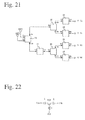
To secure isolation between the transmitting circuits and the receiving circuits, as shown in FIG. 21, a single-pole, single-throw (SPST) switch circuit 11 is preferably disposed between the high-frequency switch circuit 10 and the second diplexer circuit 25. The SPST switch circuit 11 is constituted, for instance, by a switching element, an inductance element and a capacitance element as shown in FIGS. 22-25, to control that a signal is shut when the port 10 c of the high-frequency switch circuit 10 is connected to the port 10 a or 10 b.
Embodiment 2
An example of the multi-band high-frequency circuit having the equivalent circuit shown in FIG. 3 formed in a laminate is shown in FIGS. 26-28. FIG. 26 shows the appearance of a multi-band high-frequency circuit component comprising first and second diplexer circuits 20, 25, filter circuits 30, 40, 60, first and second balanced-unbalanced circuits 50, 55, etc. in and on a laminate. FIGS. 27 and 28 show the structure of each layer in the laminate 100 constituting the high-frequency circuit component.
The laminate 100 is produced by laminating pluralities of ceramic green sheets as thick as 10-200 μm and made of, for instance, a dielectric ceramic sinterable at as low a temperature as 1000° C. or lower, each of which is provided with an electrode pattern formed by printing a conductive paste of Ag, Cu, etc., and integrally sintering them.
A lowermost green sheet 15 is covered with a ground electrode GND on its front surface, and provided with terminal electrodes for mounting to a circuit substrate on its rear surface. The terminal electrodes comprise antenna ports ANT1, ANT2, transmission ports Tx1, Tx2 for inputting unbalanced signals, receiving ports Rx1+, Rx1−, Rx2+, Rx2− for outputting balanced signals, ground ports GND, and switch circuit-controlling ports V1, V2, and these ports are connected to electrode patterns on green sheets above through via-holes (shown by black circles in the figure) formed in the green sheets. In this embodiment, the terminal electrodes in a land grid array (LGA), but may be in a ball grid array (BGA), etc.
Green sheets 1-14 are laminated on the green sheet 15. On these green sheets, the first and second diplexer circuits 20, 25, the filter circuits 30, 40, 60, and the balanced-to-unbalanced converters 50, 55 are constituted by inductance elements formed by transmission lines, and capacitance elements formed by predetermined electrode patterns, which are properly connected through via-holes. Matching circuits 80, 85 disposed between the filter circuits 30, 40 and the balanced-to-unbalanced converters 50, 55 are formed by transmission lines having predetermined length. The inductance elements and the capacitance elements may of course be mounted onto the laminate 100 as chip inductors and chip capacitors.
Each circuit is three-dimensionally formed in the laminate 100, and electrode patterns constituting the circuits are disposed such that they are separated by the ground electrode GND or do not overlap in a lamination direction, to prevent unnecessary electromagnetic interference. Transmission lines through which a 5-GHz-band, high-frequency signal passes are separate from the other electrode patterns by at least 50 μm, to prevent electromagnetic interference.
Dielectric materials may be, for instance, ceramics comprising Al, Si and Sr as main components, and Ti, Bi, Cu, Mn, Na, K, etc. as sub-components; ceramics comprising Al, Si and Sr as main components, Ca, and Pb, Na, K, etc. as sub-components; ceramics comprising Al, Mg, Si and Gd; or ceramics comprising Al, Si, Zr and Mg. The dielectric materials have dielectric constants of about 5-15. Besides the dielectric ceramics, resins and resin/ceramic composite materials may be used. Further, electrode patterns may be formed by high-temperature-sinterable metal conductors such as tungsten, molybdenum, etc. on Al2O3-based dielectric substrates, by a high-temperature cofirable ceramic (HTCC) technology.
Pluralities of land electrodes are formed on a green sheet 1, and DPDT switches (GaAs FETs), and coupling capacitors that cannot be formed in the laminate are mounted as chip parts onto the land electrodes. The land electrodes are connected to connecting lines and circuit elements in the laminate through via-holes.
Bare switches are mounted onto the land electrodes, and the land electrodes may be sealed by resins or pipes. Such multi-band high-frequency circuit components are suitably miniaturized. Incidentally, RF-ICs or base-band ICs constituting the transmitting/receiving circuits may be integrated to the laminate.
Embodiment 3
FIG. 29 shows the equivalent circuit of another multi-band high-frequency circuit. The feature of this multi-band high-frequency circuit is that the lower-frequency filter circuit in the second diplexer circuit 25 is constituted by a phase circuit Lfr1 and a bandpass filter circuit 30 having a 2.4-GHz passband. The phase circuit Lfr1 properly adjust the phase of a high-frequency signal, so that when viewed from the high-frequency switch circuit, the bandpass filter circuit 30 has high impedance in a band of 5 GHz, thereby preventing a 5-GHz-band, high-frequency signal from leaking to the receiving circuit in a 2.4-GHz band. In this embodiment, with the phase circuit Lfr1 constituted by transmission lines, the multi-band high-frequency circuit can be constituted by small numbers of circuit elements.
Embodiment 4
A multi-band high-frequency circuit in a further embodiment is shown in FIGS. 30-32. FIG. 30 shows a transmitting circuit in a multi-band high-frequency circuit comprising a coupling circuit. In this embodiment, to provide a TPC function, a coupling circuit 150 adapted to pluralities of communication systems for getting part of transmission power is disposed between the high-frequency switch circuit 10 and the first diplexer circuit 20 in the multi-band high-frequency circuit in Embodiment 1.
In this embodiment, part of output power is detected from a 2.4-GHz-band, high-frequency signal and a 5-GHz-band, high-frequency signal by the coupling circuit 150 and a detection circuit 300 comprising a detection diode (Schottky diode). Thus, detection accuracy is increased by monitoring the output power near the antenna output terminal. The coupling circuit 150 may be constituted, for instance, by a directional coupler or a coupling capacitor.
In the multi-band high-frequency circuit in this Embodiment, one coupling circuit is used in a 2.4-GHz band and a 5-GHz band. The coupling circuit has a larger coupling degree in a 5-GHz band than in a 2.4-GHz band, with the difference as large as about 5 dB. The coupling degree difference directly affects detection voltage, resulting in different detection voltage to the output power from the amplifier. With a matching circuit 200 disposed between the coupling circuit 150 and the detection circuit 300, the impedance of the coupling circuit 150 and the impedance of the detection circuit 300 are matched in a 2.4-GHz band, so that large detection voltage can be obtained even in a 2.4-GHz band with a small coupling degree (detection voltage) difference.
The matching circuit is preferably constituted by a shunt inductor connected to the output port 150 c of the coupling circuit 150, and a phase circuit connected between the coupling circuit 150 and the detection diode. In the matching adjustment of this matching circuit on a Smith chart, amplitude adjustment by the shunt inductor and phase matching by the phase circuit can be independently conducted. This simplifies the impedance matching of the coupling circuit and the detection circuit in a 2.4-GHz band.
FIG. 31 shows the equivalent circuit of a coupling circuit 150 in the multi-band high-frequency circuit comprising a directional coupler as the coupling circuit. The directional coupler is constituted by a main line STL1, a sub-line STL2 and a resistor R1, so that a transmission signal from the first diplexer circuit 20 is input to the input port 150 b of the directional coupler 150 and output from the output port 150 a. The main line STL1 and the sub-line STL2 are electromagnetically coupled, so that part of the transmission signal is output to the coupling port 150 c.
The matching circuit 200 is constituted by a shunt inductor Lss and a phase circuit Lsi, and the constants of the shunt inductor Lss and the phase circuit Lsi are set such that the output impedance of the coupling port 150 c of the directional coupling circuit is matched with the input impedance of the detection circuit 300 in a 2.4-GHz band. The shunt inductor Lss performs amplitude adjustment, and the phase circuit Lsi performs phase matching.
The detection diode Dk has an anode connected to the matching circuit 200, and a cathode connected to a voltage-smoothing circuit comprising shunt-connected capacitor Ck and resistor Rk. A high-frequency signal from the coupling circuit 150 is input to the detection diode Dk, and only a high-frequency signal exceeding its forward voltage is transmitted to the cathode, converted to DC voltage by the smoothing circuit, and input as detection voltage to a comparison control means connected to the output side of the detection circuit 300.
The comparison control means 400 is constituted by an operational amplifier, resistors, control transistors, etc., to compare an input reference signal and a detection signal supplied from the detection diode Dk to change the output power of the amplifier such that the level difference between the two signals becomes zero.
As another example of the high-frequency circuit, FIG. 32 shows a high-frequency circuit in which the coupling circuit portion shown in FIG. 31 is constituted by a coupling capacitor Cc1. In this coupling circuit, too, the coupling degree is higher by about 5 dB in a 2.4-GHz band than in a 5-GHz band, so that the detection voltage in a 2.4-GHz band can be increased by the matching circuit 200 to reduce the difference from that in a 5-GHz band.
In the circuit whose coupling circuit portion is constituted by the coupling capacitor Cc1, too, frequency change provides only little variations in the detection voltage, resulting in the reduced number of parts and miniaturization. Accordingly, such high-frequency circuit is suitable for communication systems of IEEE802.11h having a TPC function.
The multi-band high-frequency circuit of the present invention can select the most suitable channel without being influenced by noises, phasing, etc. in data communications by WLAN, and perform diversity receiving. The multi-band high-frequency circuit of the present invention can also switch the connection of multi-band antennas and transmitting circuits/receiving circuits while suppressing power consumption with few numbers of switch means.
APPLICABILITY IN INDUSTRY
With a high-frequency circuit component having the above high-frequency circuit in a small three-dimensional laminate structure, it is possible to provide a multi-band communication apparatus with a transmitting/receiving means for modulating transmission data and demodulating receiving data in each communication system, and a switch circuit controller for controlling the switching of the high-frequency switch.
The multi-band high-frequency circuit of the present invention having such features is suitable for personal computers, PC peripherals such as printers, hard disk drives, broadband rooters, etc.; electronic appliances such as facsimiles, refrigerators, standard-definition televisions, high-definition televisions, digital cameras, digital video recorders, cell phones, etc.; and signal-transmitting means in automobiles and aircrafts.

Claims (21)

1. A multi-band high-frequency circuit for performing wireless communications among pluralities of communication systems having different communication frequencies, comprising
a high-frequency switch circuit comprising switching elements for switching the connection of pluralities of multi-band antennas to transmitting circuits and receiving circuits;
a first diplexer circuit disposed between said high-frequency switch circuit and said transmitting circuits for branching a high-frequency signal into frequency bands of said communication systems;
a second diplexer circuit disposed between said high-frequency switch circuit and said receiving circuits for branching a high-frequency signal into frequency bands of said communication systems;
said first and second diplexer circuits each comprising a lower-frequency filter circuit and a higher-frequency filter circuit, a bandpass filter circuit being used as said lower-frequency filter circuit in said second diplexer circuit, or disposed between said lower-frequency filter circuit in said second diplexer circuit and said receiving circuit,
said high-frequency switch circuit comprising first to fourth ports, said first port being connected to a first multi-band antenna, said second port being connected to a second multi-band antenna, said third port being connected to said first diplexer circuit, and said fourth port being connected to said second diplexer circuit; and
said switching elements being controlled in an ON or OFF state to select a multi-band antenna for performing wireless communications and to switch the connection of the selected multi-band antenna to said transmitting circuit or said receiving circuit.
2. The multi-band high-frequency circuit according to claim 1, wherein a coupling circuit for taking a transmission power from pluralities of communication systems is disposed between said high-frequency switch circuit and said first diplexer circuit.
3. The multi-band high-frequency circuit according to claim 2, wherein said coupling circuit is constituted by a coupling capacitor, and comprises a matching circuit disposed between said coupling circuit and a detection circuit.
4. The multi-band high-frequency circuit according to claim 2, wherein said coupling circuit is constituted by a directional coupler comprising a main line and a sub-line, and comprises a grounded resistor connected to one end of said sub-line and a matching circuit disposed between the other end of said sub-line and a detection circuit.
5. The multi-band high-frequency circuit according to claim 1, wherein each of said first and second diplexer circuits is constituted by parallel-connected lower-frequency filter circuit and higher-frequency filter circuit with one end as a common port, said lower-frequency filter circuit being a filter circuit permitting a 2.4-GHz-band, high-frequency signal to pass but attenuating a 5-GHz-band, high-frequency signal, and said higher-frequency filter being a filter circuit permitting a 5-GHz-band, high-frequency signal to pass but attenuating a 2.4-GHz-band transmission signal.
6. The multi-band high-frequency circuit according to claim 5, wherein said lower-frequency filter circuit in said second diplexer circuit is constituted by a phase circuit and a bandpass filter circuit having a 2.4-GHz passband, said phase circuit controlling the impedance of said bandpass filter circuit in a band of 5 GHz to high impedance when viewed from said high-frequency switch circuit.
7. The multi-band high-frequency circuit according to claim 1, comprising a first balanced-to-unbalanced converter disposed between said lower-frequency filter circuit in said second diplexer circuit and said receiving circuit, and a second balanced-to-unbalanced converter disposed between said higher-frequency filter circuit in said second diplexer circuit and said receiving circuit.
8. The multi-band high-frequency circuit according to claim 1, comprising a transmitting/receiving means for modulating transmission data and demodulating receiving data in each communication system, and a switch circuit controller for controlling the switching of said high-frequency switch.
9. A multi-band high-frequency circuit component comprising the high-frequency circuit recited in claim 1, comprising a laminate of substrates having electrode patterns and elements mounted onto said laminate, at least part of inductance elements and capacitance elements being constituted by said electrode patterns, and at least said switching elements being mounted onto said laminate, among circuit elements constituting said high-frequency circuit.
10. A multi-band communication apparatus comprising the multi-band high-frequency circuit recited in 1.
11. A multi-band communication apparatus comprising the multi-band high-frequency circuit component recited in claim 10.
12. A multi-band high-frequency circuit for performing wireless communications among pluralities of communication systems having different communication frequencies, comprising
a high-frequency switch circuit comprising switching elements for switching the connection of one multi-band antenna to transmitting circuits and receiving circuits;
a first diplexer circuit disposed between said high-frequency switch circuit and said transmitting circuits for branching a high-frequency signal into frequency bands of said communication systems;
a second diplexer circuit disposed between said high-frequency switch circuit and said receiving circuits for branching a high-frequency signal into frequency bands of said communication systems;
said first and second diplexer circuits each comprising a lower-frequency filter circuit and a higher-frequency filter circuit, a bandpass filter circuit being used as said lower-frequency filter circuit in said second diplexer circuit, or disposed between said lower-frequency filter circuit in said second diplexer circuit and said receiving circuit;
said high-frequency switch circuit comprising first to third ports, said first port being connected to a first multi-band antenna via a matching circuit, said second port being connected to said first diplexer circuit, and said third port being connected to said second diplexer circuit; and
said switching elements being controlled in an ON or OFF state to switch the connection of said multi-band antenna to said transmitting circuit or said receiving circuit;
wherein a coupling circuit for taking a transmission power from pluralities of communication systems is disposed between said high-frequency switch circuit and said first diplexer circuit.
13. The multi-band high-frequency circuit according to claim 12, wherein said coupling circuit is constituted by a coupling capacitor, and comprises a matching circuit disposed between said coupling circuit and a detection circuit.
14. The multi-band high-frequency circuit according to claim 12, wherein said coupling circuit is constituted by a directional coupler comprising a main line and a sub-line, and comprises a grounded resistor connected to one end of said sub-line and a matching circuit disposed between the other end of said sub-line and a detection circuit.
15. The multi-band high-frequency circuit according to claim 12, wherein each of said first and second diplexer circuits is constituted by parallel-connected lower-frequency filter circuit and higher-frequency filter circuit with one end as a common port, said lower-frequency filter circuit being a filter circuit permitting a 2.4-GHz-band, high-frequency signal to pass but attenuating a 5-GHz-band, high-frequency signal, and said higher-frequency filter being a filter circuit permitting a 5-GHz-band, high-frequency signal to pass but attenuating a 2.4-GHz-band transmission signal.
16. The multi-band high-frequency circuit according to claim 15, wherein said lower-frequency filter circuit in said second diplexer circuit is constituted by a phase circuit and a bandpass filter circuit having a 2.4-GHz passband, said phase circuit controlling the impedance of said bandpass filter circuit in a band of 5 GHz to high impedance when viewed from said high-frequency switch circuit.
17. The multi-band high-frequency circuit according to claim 12, comprising a first balanced-to-unbalanced converter disposed between said lower-frequency filter circuit in said second diplexer circuit and said receiving circuit, and a second balanced-to-unbalanced converter disposed between said higher-frequency filter circuit in said second diplexer circuit and said receiving circuit.
18. The multi-band high-frequency circuit according to claim 12, comprising a transmitting/receiving means for modulating transmission data and demodulating receiving data in each communication system, and a switch circuit controller for controlling the switching of said high-frequency switch.
19. A multi-band high-frequency circuit component comprising the high-frequency circuit recited in claim 12, comprising a laminate of substrates having electrode patterns and elements mounted onto said laminate, at least part of inductance elements and capacitance elements being constituted by said electrode patterns, and at least said switching elements being mounted onto said laminate, among circuit elements constituting said high-frequency circuit.
20. A multi-band communication apparatus comprising the multi-band high-frequency circuit recited in claim 12.
21. A multi-band communication apparatus comprising the multi-band high-frequency circuit component recited in claim 20.
US10/596,372 2003-12-11 2004-12-13 Multi-band high-frequency circuit, multi-band high-frequency circuit component and multi-band communication apparatus using same Active 2025-05-27 US7518469B2 (en)

Applications Claiming Priority (3)

Application Number Priority Date Filing Date Title
JP2003413623 2003-12-11
JP2003-413623 2003-12-11
PCT/JP2004/018595 WO2005057803A1 (en) 2003-12-11 2004-12-13 Multi-band high-frequency circuit, multi-band high-frequency circuit part, and multi-band communication device using the same

Related Parent Applications (1)

Application Number Title Priority Date Filing Date
PCT/JP2004/018595 A-371-Of-International WO2005057803A1 (en) 2003-12-11 2004-12-13 Multi-band high-frequency circuit, multi-band high-frequency circuit part, and multi-band communication device using the same

Related Child Applications (1)

Application Number Title Priority Date Filing Date
US12/393,708 Division US7982554B2 (en) 2003-12-11 2009-02-26 Multi-band high-frequency circuit, multi-band high frequency circuit component and multi-band communication apparatus using same

Publications (2)

Publication Number Publication Date
US20070075803A1 US20070075803A1 (en) 2007-04-05
US7518469B2 true US7518469B2 (en) 2009-04-14

Family

ID=34675060

Family Applications (3)

Application Number Title Priority Date Filing Date
US10/596,372 Active 2025-05-27 US7518469B2 (en) 2003-12-11 2004-12-13 Multi-band high-frequency circuit, multi-band high-frequency circuit component and multi-band communication apparatus using same
US12/393,615 Active US7924117B2 (en) 2003-12-11 2009-02-26 Multi-band high-frequency circuit, multi-band high-frequency circuit component and multi-band communication apparatus using same
US12/393,708 Active US7982554B2 (en) 2003-12-11 2009-02-26 Multi-band high-frequency circuit, multi-band high frequency circuit component and multi-band communication apparatus using same

Family Applications After (2)

Application Number Title Priority Date Filing Date
US12/393,615 Active US7924117B2 (en) 2003-12-11 2009-02-26 Multi-band high-frequency circuit, multi-band high-frequency circuit component and multi-band communication apparatus using same
US12/393,708 Active US7982554B2 (en) 2003-12-11 2009-02-26 Multi-band high-frequency circuit, multi-band high frequency circuit component and multi-band communication apparatus using same

Country Status (6)

Country Link
US (3) US7518469B2 (en)
EP (1) EP1696579B1 (en)
JP (2) JP4548610B2 (en)
KR (1) KR101065344B1 (en)
CN (2) CN101645713B (en)
WO (1) WO2005057803A1 (en)

Cited By (17)

* Cited by examiner, † Cited by third party
Publication number Priority date Publication date Assignee Title
US20090017772A1 (en) * 2005-04-15 2009-01-15 Hitachi Metals, Ltd. Multiband high-frequency circuit, multiband high-frequency circuit device and multiband communications apparatus comprising same
US20110116423A1 (en) * 2009-11-17 2011-05-19 Nokia Corporation Antenna Impedance Stabilization With Stabilization Load In Second Antenna Circuitry
US20120157013A1 (en) * 2010-12-15 2012-06-21 Huawei Technologies Co., Ltd. Multi-Band Multi-Path Receiving and Transmitting Device and Method, and Base Station System
US8213878B1 (en) * 2008-09-25 2012-07-03 Rf Micro Devices, Inc. RF switch power splitter for WLAN and bluetooth coexistence
US20140321312A1 (en) * 2012-07-11 2014-10-30 Ntt Docomo, Inc. Front-end circuit and impedance adjustment method
US9923611B2 (en) 2005-09-27 2018-03-20 Qualcomm Incorporated Maximum combining in broadcast OFDM systems based on multiple receive antennas
US10454511B2 (en) * 2007-09-26 2019-10-22 Intel Mobile Communications GmbH Radio-frequency front-end and receiver
US11749893B2 (en) 2016-08-29 2023-09-05 Silicon Laboratories Inc. Apparatus for antenna impedance-matching and associated methods
US11750167B2 (en) 2017-11-27 2023-09-05 Silicon Laboratories Inc. Apparatus for radio-frequency matching networks and associated methods
US11764749B2 (en) 2016-08-29 2023-09-19 Silicon Laboratories Inc. Apparatus with partitioned radio frequency antenna and matching network and associated methods
US11764473B2 (en) 2016-08-29 2023-09-19 Silicon Laboratories Inc. Apparatus with partitioned radio frequency antenna and matching network and associated methods
US11769949B2 (en) 2016-08-29 2023-09-26 Silicon Laboratories Inc. Apparatus with partitioned radio frequency antenna and matching network and associated methods
US11862872B2 (en) 2021-09-30 2024-01-02 Silicon Laboratories Inc. Apparatus for antenna optimization and associated methods
US11894826B2 (en) 2017-12-18 2024-02-06 Silicon Laboratories Inc. Radio-frequency apparatus with multi-band balun and associated methods
US11894621B2 (en) 2017-12-18 2024-02-06 Silicon Laboratories Inc. Radio-frequency apparatus with multi-band balun with improved performance and associated methods
US11894622B2 (en) 2016-08-29 2024-02-06 Silicon Laboratories Inc. Antenna structure with double-slotted loop and associated methods
US11916514B2 (en) 2017-11-27 2024-02-27 Silicon Laboratories Inc. Radio-frequency apparatus with multi-band wideband balun and associated methods

Families Citing this family (57)

* Cited by examiner, † Cited by third party
Publication number Priority date Publication date Assignee Title
JP5137167B2 (en) * 2004-06-25 2013-02-06 日立金属株式会社 BANDPASS FILTER, HIGH FREQUENCY CIRCUIT, HIGH FREQUENCY CIRCUIT COMPONENT, AND MULTIBAND COMMUNICATION DEVICE USING THEM
EP1768269B1 (en) * 2004-06-30 2016-06-22 Hitachi Metals, Ltd. High frequency circuit, high frequency component, and multi-band communication apparatus
WO2006120600A1 (en) * 2005-05-06 2006-11-16 Koninklijke Philips Electronics N.V. Wireless medical monitoring device
KR100664221B1 (en) * 2005-09-16 2007-01-04 엘지전자 주식회사 Dual mode fem and terminal having the dual mode fem
US8497762B2 (en) * 2006-03-07 2013-07-30 Tyco Fire & Security Gmbh Network control
KR101362687B1 (en) * 2007-01-12 2014-02-13 에이저 시스템즈 엘엘시 Scanning available wireless-device services in multiple wireless-radio technology communication systems
JP2010518689A (en) 2007-02-02 2010-05-27 トムソン ライセンシング Apparatus and method for detecting ATSC signal with low S / N ratio
CN101420238B (en) * 2007-10-26 2012-07-25 海华科技股份有限公司 Filtering device and method used for dual frequency band sensing circuit
CN101604993B (en) * 2008-06-11 2013-02-13 联想(北京)有限公司 Multiaerial system and method for radiating radio frequency signals
US8565814B2 (en) * 2008-08-28 2013-10-22 Intel Mobile Communications GmbH Radio frequency communication devices and methods
CN101729086B (en) * 2008-10-10 2013-05-08 鸿富锦精密工业(深圳)有限公司 Wireless communication device
CN102439789B (en) * 2008-12-24 2014-08-06 豪沃基金有限责任公司 RF front-end module and antenna systems
US20100309901A1 (en) * 2009-06-03 2010-12-09 Harris Corporation Systems and methods for maintaining a controlled power output at an antenna port over a range of frequencies defined by two or more frequency bands
JP5273388B2 (en) * 2009-09-08 2013-08-28 日本電気株式会社 Multi-band high frequency power monitor circuit
US20110117869A1 (en) * 2009-11-18 2011-05-19 Ryan Woodings Multiple band portable spectrum analyzer
EP2532100B1 (en) 2010-02-03 2019-06-05 BAE Systems PLC Antenna diversity apparatus
DE102010012603B4 (en) * 2010-03-24 2019-09-12 Snaptrack, Inc. Front end module and method for operation in different circuit environments
WO2012005787A1 (en) * 2010-07-08 2012-01-12 Microsemi Corporation Improved architecture for coexistence of multiple band radios
US8666328B2 (en) 2010-07-12 2014-03-04 Apple Inc. Wireless circuitry with reduced harmonic interference
CN103620971B (en) 2011-06-27 2016-05-04 株式会社村田制作所 High-frequency model
US20130016633A1 (en) 2011-07-14 2013-01-17 Lum Nicholas W Wireless Circuitry for Simultaneously Receiving Radio-frequency Transmissions in Different Frequency Bands
CN103718469B (en) * 2011-08-01 2016-06-08 株式会社村田制作所 High-frequency model
US10009058B2 (en) 2012-06-18 2018-06-26 Qorvo Us, Inc. RF front-end circuitry for receive MIMO signals
US20140015731A1 (en) 2012-07-11 2014-01-16 Rf Micro Devices, Inc. Contact mems architecture for improved cycle count and hot-switching and esd
JP5668029B2 (en) * 2012-07-17 2015-02-12 株式会社Nttドコモ Radio circuit, frequency pair determination method
US8774068B2 (en) * 2012-10-11 2014-07-08 Sony Corporation Dual swapping switches to meet linearity demands of carrier aggregation
US20140169243A1 (en) * 2012-12-18 2014-06-19 Rf Micro Devices, Inc. Mobile communication circuitry for three or more antennas
JP5983773B2 (en) 2012-12-26 2016-09-06 株式会社村田製作所 Switch module
CN104854792B (en) * 2013-10-17 2018-11-06 株式会社村田制作所 High-frequency circuit
US9654169B2 (en) 2014-04-22 2017-05-16 Skyworks Solutions, Inc. Apparatus and methods for multi-band radio frequency signal routing
US10312960B2 (en) 2014-08-12 2019-06-04 Qorvo Us, Inc. Switchable RF transmit/receive multiplexer
US9843342B2 (en) * 2014-08-12 2017-12-12 Qorvo Us, Inc. Tunable RF transmit/receive multiplexer
US9780866B2 (en) 2014-08-12 2017-10-03 Qorvo Us, Inc. Configurable RF transmit/receive multiplexer
DK3283848T3 (en) * 2015-04-17 2019-09-02 Landis & Gyr Ag ELECTRICITY METER AND ADAPTER MODULE HEREIN
CN104850885B (en) * 2015-04-30 2019-03-29 东莞电子科技大学电子信息工程研究院 A kind of middle low-frequency electronic label and its signaling method
US10432235B2 (en) * 2015-06-09 2019-10-01 Skyworks Solutions, Inc. Carrier aggregation using diplexers
CN106301629A (en) * 2015-06-12 2017-01-04 中兴通讯股份有限公司 Broadband multi-band signal detecting method and device and wireless communication system
WO2016208559A1 (en) * 2015-06-24 2016-12-29 株式会社村田製作所 Demultiplexing circuit
US20170012763A1 (en) * 2015-07-08 2017-01-12 Mediatek Inc. Multiband Filter Circuitry, Multiband Duplexer Circuitry, and Related Radio-Frequency System
KR102139764B1 (en) * 2015-09-21 2020-07-31 삼성전기주식회사 Communication module and front-end module included thereof
US10547336B2 (en) * 2015-10-23 2020-01-28 Qorvo Us, Inc. Radio frequency circuitry for carrier aggregation
KR102021252B1 (en) * 2015-10-26 2019-09-11 가부시키가이샤 무라타 세이사쿠쇼 Switch module
JP2017130893A (en) * 2016-01-22 2017-07-27 アルプス電気株式会社 Communication module
US10560867B2 (en) 2016-12-29 2020-02-11 Qorvo Us, Inc. Reducing intermodulation distortion in a radio frequency circuit
US10659121B2 (en) 2017-03-15 2020-05-19 Skyworks Solutions, Inc. Apparatus and methods for radio frequency front-ends
KR101912288B1 (en) 2017-06-12 2018-10-29 삼성전기 주식회사 Band selection switch of power amplifier system
US10623130B2 (en) * 2017-07-27 2020-04-14 Rolls-Royce North American Technologes, Inc. Determining a frequency for propulsor engine communication sessions
US10439656B2 (en) * 2017-11-28 2019-10-08 Schlage Lock Company Llc Communication circuit with single element antenna for multi-frequency applications
US11006460B2 (en) 2017-11-28 2021-05-11 Mediatek Singapore Pte. Ltd. Wireless communication with dedicated dynamic frequency selection
US10355723B2 (en) * 2017-11-28 2019-07-16 Schlage Lock Company Llc Communication circuit with single element antenna for multi-frequency applications
CN108111176B (en) * 2017-12-08 2021-02-19 Tcl移动通信科技(宁波)有限公司 Double-antenna radio frequency power detection circuit, device and mobile terminal
CN113366761A (en) * 2019-01-23 2021-09-07 株式会社村田制作所 High-frequency front-end circuit and communication device
CN109560833B (en) * 2019-01-28 2022-01-11 惠州Tcl移动通信有限公司 Downlink carrier aggregation radio frequency circuit, antenna device and electronic equipment
CN109861735B (en) * 2019-03-22 2022-07-15 维沃移动通信有限公司 Radio frequency front-end circuit and mobile terminal
CN112653439B (en) * 2020-12-16 2022-11-04 电子科技大学 Multiband single-pole double-throw switch
CN112909464B (en) * 2021-01-25 2021-11-02 中天通信技术有限公司 Microstrip combiner with uniform impedance branch loading
CN114826230B (en) * 2022-04-28 2023-04-25 电子科技大学 Ultra-wideband single-pole multi-throw radio frequency switch applying reconfigurable filter network

Citations (17)

* Cited by examiner, † Cited by third party
Publication number Priority date Publication date Assignee Title
US5784687A (en) * 1994-08-30 1998-07-21 Matsushita Electric Industrial Co., Ltd. Transmitting-receiving circuit for radiocommunication apparatus, semiconductor integrated circuit device including the circuit, and radiocommunication apparatus including the same
JP2000269831A (en) 1999-03-17 2000-09-29 Sharp Corp Radio terminal adopting transmission power control system
WO2001048935A1 (en) 1999-12-28 2001-07-05 Hitachi Metals, Ltd. High-frequency switch, high-frequency switch module, and wireless communication device
US20010027119A1 (en) 2000-03-23 2001-10-04 Murata Manufacturing Co., Ltd. Nagaokakyo-Shi, Japan Mobile communication device and high-frequency composite unit used in the same
JP2001285114A (en) 2000-03-28 2001-10-12 Sharp Corp Plural bands communication equipment sharing antenna
JP2002026624A (en) 2000-07-07 2002-01-25 Nippon Tungsten Co Ltd Dielectric antenna module
JP2002118487A (en) 2000-10-06 2002-04-19 Matsushita Electric Ind Co Ltd High-frequency composite switch module
JP2002208873A (en) 2001-01-09 2002-07-26 Hitachi Metals Ltd Antenna switch laminated module composite part
JP2003046408A (en) 2001-08-02 2003-02-14 Ngk Spark Plug Co Ltd Hybrid high frequency component and mobile communication equipment
JP2003152590A (en) 2001-11-14 2003-05-23 Ngk Spark Plug Co Ltd Antenna-switching module
JP2003169008A (en) 2001-11-28 2003-06-13 Internatl Business Mach Corp <Ibm> Multi-band communication device and its communication method
US20030207668A1 (en) 2002-05-03 2003-11-06 Mcfarland William J. Dual frequency band wireless lan
US20060044080A1 (en) * 2002-10-25 2006-03-02 Hitachi Metals, Ltd. Balanced-unbalanced type multiband filer module
US7057472B2 (en) * 2001-08-10 2006-06-06 Hitachi Metals, Ltd. Bypass filter, multi-band antenna switch circuit, and layered module composite part and communication device using them
US7127269B2 (en) * 2003-12-30 2006-10-24 Delta Electronics, Inc. Front-end module for multi-band and multi-mode wireless network system
US20060286942A1 (en) * 2005-06-16 2006-12-21 Tdk Corporation High frequency module
US7206551B2 (en) * 2003-08-08 2007-04-17 Tdk Corporation High frequency switch module and multi-layer substrate for high frequency switch module

Family Cites Families (39)

* Cited by examiner, † Cited by third party
Publication number Priority date Publication date Assignee Title
JPH0749043Y2 (en) * 1990-01-10 1995-11-13 三菱電機株式会社 Pneumatic actuator
KR960000775B1 (en) * 1990-10-19 1996-01-12 닛본덴기 가부시끼가이샤 Output level control circuit for high freq power amp
JP3081076B2 (en) * 1993-03-10 2000-08-28 松下電器産業株式会社 Antenna diversity method in wireless communication device
JPH08293846A (en) * 1995-04-19 1996-11-05 Sony Corp Transmission/reception device
US5768691A (en) * 1996-08-07 1998-06-16 Nokia Mobile Phones Limited Antenna switching circuits for radio telephones
US5884149A (en) * 1997-02-13 1999-03-16 Nokia Mobile Phones Limited Mobile station having dual band RF detector and gain control
JPH10294634A (en) * 1997-02-19 1998-11-04 Murata Mfg Co Ltd Filter
JPH10247801A (en) * 1997-03-04 1998-09-14 Murata Mfg Co Ltd Rf switch circuit and transmission reception common use device
US6941120B2 (en) * 1997-07-29 2005-09-06 Gray Electronics, Inc. Apparatus and method for automatically programming frequency scanning radio receivers
DE19842706A1 (en) * 1998-09-17 2000-03-23 Siemens Ag Multi-band aerial switch for multi-band mobile radio telephone
JP2000278168A (en) * 1999-03-25 2000-10-06 Murata Mfg Co Ltd High frequency composite component and radio communication unit using the same
JP4232879B2 (en) * 1999-09-02 2009-03-04 パナソニック株式会社 Communication device
JP2001185902A (en) * 1999-12-27 2001-07-06 Murata Mfg Co Ltd Composite high-frequency component and communication device using same
JP2001257619A (en) * 2000-03-14 2001-09-21 Kenwood Corp Antenna switch circuit
JP2001267957A (en) * 2000-03-15 2001-09-28 Ngk Insulators Ltd Transmitter-receiver
JP2001267955A (en) * 2000-03-22 2001-09-28 Matsushita Electric Ind Co Ltd Composite wireless terminal and wireless system using the same
JP3707351B2 (en) * 2000-03-31 2005-10-19 株式会社村田製作所 High frequency module and wireless device using the same
JP2002043892A (en) * 2000-07-31 2002-02-08 Kyocera Corp Surface acoustic wave device and communication terminal using the device
WO2002017504A1 (en) * 2000-08-22 2002-02-28 Hitachi Metals, Ltd. Laminated high-frequency switch module
JP2002100909A (en) * 2000-09-26 2002-04-05 Murata Mfg Co Ltd Directional coupler and communication apparatus using the same
KR20020040008A (en) * 2000-11-23 2002-05-30 송재인 The eliminative circuit and method of noise and external noise of input signal
JP2002190769A (en) * 2000-12-21 2002-07-05 Sharp Corp Communication equipment and communication system of mobile object
JP2002325049A (en) * 2001-04-26 2002-11-08 Hitachi Ltd Communication terminal sharable by different communication systems, antenna duplexer and power amplifier for use therein
JP3800504B2 (en) * 2001-05-15 2006-07-26 Tdk株式会社 Front-end module
JP3772771B2 (en) * 2001-05-18 2006-05-10 松下電器産業株式会社 Multiband high frequency switch
JP2002368512A (en) * 2001-06-12 2002-12-20 Sony Corp Power loss suppression antenna circuit and portable terminal provided with the same
JP2003037520A (en) * 2001-07-26 2003-02-07 Murata Mfg Co Ltd Radio frequency switch
JP2003061150A (en) * 2001-08-15 2003-02-28 Nippon Telegr & Teleph Corp <Ntt> Wireless packet terminal and control method for the wireless packet terminal
JP4006680B2 (en) * 2001-08-31 2007-11-14 日立金属株式会社 Multiband antenna switch circuit, multiband antenna switch laminated module composite component, and communication apparatus using the same
JP2003087150A (en) * 2001-09-14 2003-03-20 Matsushita Electric Ind Co Ltd High frequency composite switch module
JP3830369B2 (en) * 2001-09-27 2006-10-04 日本特殊陶業株式会社 High frequency circuit, composite high frequency component, and communication device using the same
KR20030056243A (en) * 2001-12-27 2003-07-04 삼성전기주식회사 Triplexer circuit and chip multilayer triplexer
JP3952791B2 (en) * 2002-01-30 2007-08-01 ソニー株式会社 Communication device and communication method
DE60334888D1 (en) * 2002-01-31 2010-12-23 Hitachi Metals Ltd SWITCHING NETWORK AND COMPOSED HIGH FREQUENCY PART
JP2003249935A (en) * 2002-02-26 2003-09-05 Oki Electric Ind Co Ltd Radio lan system
JP3821220B2 (en) * 2002-03-28 2006-09-13 ソニー株式会社 Base station wireless communication device
JP3093601U (en) * 2002-10-23 2003-05-16 アルプス電気株式会社 Dual band transceiver
US7412496B2 (en) * 2003-08-22 2008-08-12 Emc Corporation Management of the file-modification time attribute in a multi-processor file server system
JP4134005B2 (en) * 2004-11-15 2008-08-13 Tdk株式会社 High frequency module

Patent Citations (20)

* Cited by examiner, † Cited by third party
Publication number Priority date Publication date Assignee Title
US5784687A (en) * 1994-08-30 1998-07-21 Matsushita Electric Industrial Co., Ltd. Transmitting-receiving circuit for radiocommunication apparatus, semiconductor integrated circuit device including the circuit, and radiocommunication apparatus including the same
JP2000269831A (en) 1999-03-17 2000-09-29 Sharp Corp Radio terminal adopting transmission power control system
WO2001048935A1 (en) 1999-12-28 2001-07-05 Hitachi Metals, Ltd. High-frequency switch, high-frequency switch module, and wireless communication device
US20020183016A1 (en) 1999-12-28 2002-12-05 Shigeru Kemmochi High-frequency switch circuit, high-frequency switch module and wireless communication device
US20010027119A1 (en) 2000-03-23 2001-10-04 Murata Manufacturing Co., Ltd. Nagaokakyo-Shi, Japan Mobile communication device and high-frequency composite unit used in the same
JP2001274723A (en) 2000-03-23 2001-10-05 Murata Mfg Co Ltd Mobile communication unit and high-frequency compound component used therefor
JP2001285114A (en) 2000-03-28 2001-10-12 Sharp Corp Plural bands communication equipment sharing antenna
JP2002026624A (en) 2000-07-07 2002-01-25 Nippon Tungsten Co Ltd Dielectric antenna module
US20030048154A1 (en) 2000-10-06 2003-03-13 Yuki Satoh High-frequency composite switch module
JP2002118487A (en) 2000-10-06 2002-04-19 Matsushita Electric Ind Co Ltd High-frequency composite switch module
JP2002208873A (en) 2001-01-09 2002-07-26 Hitachi Metals Ltd Antenna switch laminated module composite part
JP2003046408A (en) 2001-08-02 2003-02-14 Ngk Spark Plug Co Ltd Hybrid high frequency component and mobile communication equipment
US7057472B2 (en) * 2001-08-10 2006-06-06 Hitachi Metals, Ltd. Bypass filter, multi-band antenna switch circuit, and layered module composite part and communication device using them
JP2003152590A (en) 2001-11-14 2003-05-23 Ngk Spark Plug Co Ltd Antenna-switching module
JP2003169008A (en) 2001-11-28 2003-06-13 Internatl Business Mach Corp <Ibm> Multi-band communication device and its communication method
US20030207668A1 (en) 2002-05-03 2003-11-06 Mcfarland William J. Dual frequency band wireless lan
US20060044080A1 (en) * 2002-10-25 2006-03-02 Hitachi Metals, Ltd. Balanced-unbalanced type multiband filer module
US7206551B2 (en) * 2003-08-08 2007-04-17 Tdk Corporation High frequency switch module and multi-layer substrate for high frequency switch module
US7127269B2 (en) * 2003-12-30 2006-10-24 Delta Electronics, Inc. Front-end module for multi-band and multi-mode wireless network system
US20060286942A1 (en) * 2005-06-16 2006-12-21 Tdk Corporation High frequency module

Cited By (30)

* Cited by examiner, † Cited by third party
Publication number Priority date Publication date Assignee Title
US20090017772A1 (en) * 2005-04-15 2009-01-15 Hitachi Metals, Ltd. Multiband high-frequency circuit, multiband high-frequency circuit device and multiband communications apparatus comprising same
US7885613B2 (en) * 2005-04-15 2011-02-08 Hitachi Metals, Ltd. Multiband high-frequency circuit, multiband high-frequency circuit device and multiband communications apparatus comprising same
US20110096705A1 (en) * 2005-04-15 2011-04-28 Hitachi Metals, Ltd. Multiband high-frequency circuit, multiband high-frequency circuit device and multiband communications apparatus comprising same
US8315577B2 (en) 2005-04-15 2012-11-20 Hitachi Metals, Ltd. Multiband high-frequency circuit, multiband high-frequency circuit device and multiband communications apparatus comprising same
US9923611B2 (en) 2005-09-27 2018-03-20 Qualcomm Incorporated Maximum combining in broadcast OFDM systems based on multiple receive antennas
US10454511B2 (en) * 2007-09-26 2019-10-22 Intel Mobile Communications GmbH Radio-frequency front-end and receiver
US8213878B1 (en) * 2008-09-25 2012-07-03 Rf Micro Devices, Inc. RF switch power splitter for WLAN and bluetooth coexistence
US20110116423A1 (en) * 2009-11-17 2011-05-19 Nokia Corporation Antenna Impedance Stabilization With Stabilization Load In Second Antenna Circuitry
US8774067B2 (en) * 2009-11-17 2014-07-08 Nokia Corporation Antenna impedance stabilization with stabilization load in second antenna circuitry
US20120157013A1 (en) * 2010-12-15 2012-06-21 Huawei Technologies Co., Ltd. Multi-Band Multi-Path Receiving and Transmitting Device and Method, and Base Station System
US20140364072A1 (en) * 2010-12-15 2014-12-11 Huawei Technologies Co., Ltd. Multi-Band Multi-Path Receiving and Transmitting Device and Method, and Base Station System
US9124311B2 (en) * 2010-12-15 2015-09-01 Huawei Technologies Co., Ltd. Multi-band multi-path receiving and transmitting device and method, and base station system
US9130604B2 (en) * 2010-12-15 2015-09-08 Huawei Technologies Co., Ltd. Multi-band multi-path receiving and transmitting device and method, and base station system
US9148178B2 (en) * 2010-12-15 2015-09-29 Huawei Technologies Co., Ltd. Multi-band multi-path receiving and transmitting device and method, and base station system
US10826555B2 (en) * 2010-12-15 2020-11-03 Huawei Technologies Co., Ltd. Multi-band multi-path receiving and transmitting device and method, and base station system
US9369156B2 (en) * 2010-12-15 2016-06-14 Huawei Technologies Co., Ltd. Multi-band multi-path receiving and transmitting device and method, and base station system
US20160269071A1 (en) * 2010-12-15 2016-09-15 Huawei Technologies Co., Ltd. Multi-Band Multi-Path Receiving and Transmitting Device and Method, and Base Station System
US20130273975A1 (en) * 2010-12-15 2013-10-17 Huawei Technologies Co., Ltd. Multi-band multi-path receiving and transmitting device and method, and base station system
US9337990B2 (en) * 2012-07-11 2016-05-10 Ntt Docomo, Inc. Front-end circuit and impedance adjustment method
US20140321312A1 (en) * 2012-07-11 2014-10-30 Ntt Docomo, Inc. Front-end circuit and impedance adjustment method
US11749893B2 (en) 2016-08-29 2023-09-05 Silicon Laboratories Inc. Apparatus for antenna impedance-matching and associated methods
US11764749B2 (en) 2016-08-29 2023-09-19 Silicon Laboratories Inc. Apparatus with partitioned radio frequency antenna and matching network and associated methods
US11764473B2 (en) 2016-08-29 2023-09-19 Silicon Laboratories Inc. Apparatus with partitioned radio frequency antenna and matching network and associated methods
US11769949B2 (en) 2016-08-29 2023-09-26 Silicon Laboratories Inc. Apparatus with partitioned radio frequency antenna and matching network and associated methods
US11894622B2 (en) 2016-08-29 2024-02-06 Silicon Laboratories Inc. Antenna structure with double-slotted loop and associated methods
US11750167B2 (en) 2017-11-27 2023-09-05 Silicon Laboratories Inc. Apparatus for radio-frequency matching networks and associated methods
US11916514B2 (en) 2017-11-27 2024-02-27 Silicon Laboratories Inc. Radio-frequency apparatus with multi-band wideband balun and associated methods
US11894826B2 (en) 2017-12-18 2024-02-06 Silicon Laboratories Inc. Radio-frequency apparatus with multi-band balun and associated methods
US11894621B2 (en) 2017-12-18 2024-02-06 Silicon Laboratories Inc. Radio-frequency apparatus with multi-band balun with improved performance and associated methods
US11862872B2 (en) 2021-09-30 2024-01-02 Silicon Laboratories Inc. Apparatus for antenna optimization and associated methods

Also Published As

Publication number Publication date
EP1696579A1 (en) 2006-08-30
EP1696579A4 (en) 2009-04-08
CN100547941C (en) 2009-10-07
KR20060103281A (en) 2006-09-28
KR101065344B1 (en) 2011-09-16
CN101645713A (en) 2010-02-10
CN1894862A (en) 2007-01-10
JP2010252346A (en) 2010-11-04
WO2005057803A1 (en) 2005-06-23
JPWO2005057803A1 (en) 2008-04-17
CN101645713B (en) 2013-09-11
JP4548610B2 (en) 2010-09-22
US20070075803A1 (en) 2007-04-05
US20090206948A1 (en) 2009-08-20
US7982554B2 (en) 2011-07-19
US20090201099A1 (en) 2009-08-13
US7924117B2 (en) 2011-04-12
EP1696579B1 (en) 2013-02-20

Similar Documents

Publication Publication Date Title
US7518469B2 (en) Multi-band high-frequency circuit, multi-band high-frequency circuit component and multi-band communication apparatus using same
US7773956B2 (en) Multi-band high frequency circuit, multi-band high-frequency component and multi-band communications apparatus
CN101438505B (en) High frequency circuit, high frequency part, and communication device
US8315577B2 (en) Multiband high-frequency circuit, multiband high-frequency circuit device and multiband communications apparatus comprising same
EP1710925B1 (en) Multi-band high-frequency circuit
US8131226B1 (en) Multi-band-high-frequency circuit, multi-band high-frequency circuit component and multi-band communication apparatus using same
US7356349B2 (en) High-frequency module and communication apparatus
JP2006304081A (en) High frequency circuit, high frequency circuit component and communication equipment using it
JP4288529B2 (en) High frequency components and multiband communication devices
JP4702620B2 (en) High frequency switch module
JP2005354407A (en) High frequency circuit, high frequency component and multiband communication apparatus using the same
JP2006237978A (en) Multi-band high-frequency module and multi-band communication device using the same
JP5137167B2 (en) BANDPASS FILTER, HIGH FREQUENCY CIRCUIT, HIGH FREQUENCY CIRCUIT COMPONENT, AND MULTIBAND COMMUNICATION DEVICE USING THEM

Legal Events

Date Code Title Description
AS Assignment

Owner name: HITACHI METALS, LTD., JAPAN

Free format text: ASSIGNMENT OF ASSIGNORS INTEREST;ASSIGNORS:KEMMOCHI, SHIGERU;FUKAMACHI, KEISUKE;HAGIWARA, KAZUHIRO;AND OTHERS;REEL/FRAME:017855/0134

Effective date: 20060608

FEPP Fee payment procedure

Free format text: PAYOR NUMBER ASSIGNED (ORIGINAL EVENT CODE: ASPN); ENTITY STATUS OF PATENT OWNER: LARGE ENTITY

STCF Information on status: patent grant

Free format text: PATENTED CASE

FPAY Fee payment

Year of fee payment: 4

FPAY Fee payment

Year of fee payment: 8

MAFP Maintenance fee payment

Free format text: PAYMENT OF MAINTENANCE FEE, 12TH YEAR, LARGE ENTITY (ORIGINAL EVENT CODE: M1553); ENTITY STATUS OF PATENT OWNER: LARGE ENTITY

Year of fee payment: 12

AS Assignment

Owner name: HITACHI METALS, LTD., JAPAN

Free format text: CHANGE OF ADDRESS;ASSIGNOR:HITACHI METALS, LTD.;REEL/FRAME:057778/0737

Effective date: 20151202

AS Assignment

Owner name: MURATA MANUFACTURING CO., LTD., JAPAN

Free format text: ASSIGNMENT OF ASSIGNORS INTEREST;ASSIGNOR:HITACHI METALS, LTD.;REEL/FRAME:057780/0617

Effective date: 20210802