US7523852B2 - Solder interconnect structure and method using injection molded solder - Google Patents
Solder interconnect structure and method using injection molded solder Download PDFInfo
- Publication number
- US7523852B2 US7523852B2 US11/005,557 US555704A US7523852B2 US 7523852 B2 US7523852 B2 US 7523852B2 US 555704 A US555704 A US 555704A US 7523852 B2 US7523852 B2 US 7523852B2
- Authority
- US
- United States
- Prior art keywords
- solder
- columns
- electrical connection
- connection surfaces
- recited
- Prior art date
- Legal status (The legal status is an assumption and is not a legal conclusion. Google has not performed a legal analysis and makes no representation as to the accuracy of the status listed.)
- Expired - Fee Related
Links
Images


Classifications
-
- H—ELECTRICITY
- H05—ELECTRIC TECHNIQUES NOT OTHERWISE PROVIDED FOR
- H05K—PRINTED CIRCUITS; CASINGS OR CONSTRUCTIONAL DETAILS OF ELECTRIC APPARATUS; MANUFACTURE OF ASSEMBLAGES OF ELECTRICAL COMPONENTS
- H05K3/00—Apparatus or processes for manufacturing printed circuits
- H05K3/30—Assembling printed circuits with electric components, e.g. with resistor
- H05K3/32—Assembling printed circuits with electric components, e.g. with resistor electrically connecting electric components or wires to printed circuits
- H05K3/34—Assembling printed circuits with electric components, e.g. with resistor electrically connecting electric components or wires to printed circuits by soldering
- H05K3/341—Surface mounted components
- H05K3/3431—Leadless components
- H05K3/3436—Leadless components having an array of bottom contacts, e.g. pad grid array or ball grid array components
-
- B—PERFORMING OPERATIONS; TRANSPORTING
- B23—MACHINE TOOLS; METAL-WORKING NOT OTHERWISE PROVIDED FOR
- B23K—SOLDERING OR UNSOLDERING; WELDING; CLADDING OR PLATING BY SOLDERING OR WELDING; CUTTING BY APPLYING HEAT LOCALLY, e.g. FLAME CUTTING; WORKING BY LASER BEAM
- B23K35/00—Rods, electrodes, materials, or media, for use in soldering, welding, or cutting
- B23K35/22—Rods, electrodes, materials, or media, for use in soldering, welding, or cutting characterised by the composition or nature of the material
- B23K35/24—Selection of soldering or welding materials proper
- B23K35/26—Selection of soldering or welding materials proper with the principal constituent melting at less than 400 degrees C
-
- H—ELECTRICITY
- H01—ELECTRIC ELEMENTS
- H01L—SEMICONDUCTOR DEVICES NOT COVERED BY CLASS H10
- H01L24/00—Arrangements for connecting or disconnecting semiconductor or solid-state bodies; Methods or apparatus related thereto
- H01L24/01—Means for bonding being attached to, or being formed on, the surface to be connected, e.g. chip-to-package, die-attach, "first-level" interconnects; Manufacturing methods related thereto
- H01L24/10—Bump connectors ; Manufacturing methods related thereto
- H01L24/11—Manufacturing methods
-
- H—ELECTRICITY
- H01—ELECTRIC ELEMENTS
- H01L—SEMICONDUCTOR DEVICES NOT COVERED BY CLASS H10
- H01L24/00—Arrangements for connecting or disconnecting semiconductor or solid-state bodies; Methods or apparatus related thereto
- H01L24/01—Means for bonding being attached to, or being formed on, the surface to be connected, e.g. chip-to-package, die-attach, "first-level" interconnects; Manufacturing methods related thereto
- H01L24/10—Bump connectors ; Manufacturing methods related thereto
- H01L24/12—Structure, shape, material or disposition of the bump connectors prior to the connecting process
-
- H—ELECTRICITY
- H05—ELECTRIC TECHNIQUES NOT OTHERWISE PROVIDED FOR
- H05K—PRINTED CIRCUITS; CASINGS OR CONSTRUCTIONAL DETAILS OF ELECTRIC APPARATUS; MANUFACTURE OF ASSEMBLAGES OF ELECTRICAL COMPONENTS
- H05K3/00—Apparatus or processes for manufacturing printed circuits
- H05K3/30—Assembling printed circuits with electric components, e.g. with resistor
- H05K3/32—Assembling printed circuits with electric components, e.g. with resistor electrically connecting electric components or wires to printed circuits
- H05K3/34—Assembling printed circuits with electric components, e.g. with resistor electrically connecting electric components or wires to printed circuits by soldering
- H05K3/3457—Solder materials or compositions; Methods of application thereof
- H05K3/3468—Applying molten solder
-
- H—ELECTRICITY
- H01—ELECTRIC ELEMENTS
- H01L—SEMICONDUCTOR DEVICES NOT COVERED BY CLASS H10
- H01L2224/00—Indexing scheme for arrangements for connecting or disconnecting semiconductor or solid-state bodies and methods related thereto as covered by H01L24/00
- H01L2224/01—Means for bonding being attached to, or being formed on, the surface to be connected, e.g. chip-to-package, die-attach, "first-level" interconnects; Manufacturing methods related thereto
- H01L2224/02—Bonding areas; Manufacturing methods related thereto
- H01L2224/04—Structure, shape, material or disposition of the bonding areas prior to the connecting process
- H01L2224/05—Structure, shape, material or disposition of the bonding areas prior to the connecting process of an individual bonding area
- H01L2224/0554—External layer
- H01L2224/0556—Disposition
- H01L2224/05568—Disposition the whole external layer protruding from the surface
-
- H—ELECTRICITY
- H01—ELECTRIC ELEMENTS
- H01L—SEMICONDUCTOR DEVICES NOT COVERED BY CLASS H10
- H01L2224/00—Indexing scheme for arrangements for connecting or disconnecting semiconductor or solid-state bodies and methods related thereto as covered by H01L24/00
- H01L2224/01—Means for bonding being attached to, or being formed on, the surface to be connected, e.g. chip-to-package, die-attach, "first-level" interconnects; Manufacturing methods related thereto
- H01L2224/02—Bonding areas; Manufacturing methods related thereto
- H01L2224/04—Structure, shape, material or disposition of the bonding areas prior to the connecting process
- H01L2224/05—Structure, shape, material or disposition of the bonding areas prior to the connecting process of an individual bonding area
- H01L2224/0554—External layer
- H01L2224/05573—Single external layer
-
- H—ELECTRICITY
- H01—ELECTRIC ELEMENTS
- H01L—SEMICONDUCTOR DEVICES NOT COVERED BY CLASS H10
- H01L2224/00—Indexing scheme for arrangements for connecting or disconnecting semiconductor or solid-state bodies and methods related thereto as covered by H01L24/00
- H01L2224/01—Means for bonding being attached to, or being formed on, the surface to be connected, e.g. chip-to-package, die-attach, "first-level" interconnects; Manufacturing methods related thereto
- H01L2224/10—Bump connectors; Manufacturing methods related thereto
- H01L2224/12—Structure, shape, material or disposition of the bump connectors prior to the connecting process
- H01L2224/13—Structure, shape, material or disposition of the bump connectors prior to the connecting process of an individual bump connector
- H01L2224/13001—Core members of the bump connector
- H01L2224/13075—Plural core members
- H01L2224/1308—Plural core members being stacked
- H01L2224/13082—Two-layer arrangements
-
- H—ELECTRICITY
- H01—ELECTRIC ELEMENTS
- H01L—SEMICONDUCTOR DEVICES NOT COVERED BY CLASS H10
- H01L2224/00—Indexing scheme for arrangements for connecting or disconnecting semiconductor or solid-state bodies and methods related thereto as covered by H01L24/00
- H01L2224/01—Means for bonding being attached to, or being formed on, the surface to be connected, e.g. chip-to-package, die-attach, "first-level" interconnects; Manufacturing methods related thereto
- H01L2224/10—Bump connectors; Manufacturing methods related thereto
- H01L2224/12—Structure, shape, material or disposition of the bump connectors prior to the connecting process
- H01L2224/13—Structure, shape, material or disposition of the bump connectors prior to the connecting process of an individual bump connector
- H01L2224/13001—Core members of the bump connector
- H01L2224/13099—Material
- H01L2224/131—Material with a principal constituent of the material being a metal or a metalloid, e.g. boron [B], silicon [Si], germanium [Ge], arsenic [As], antimony [Sb], tellurium [Te] and polonium [Po], and alloys thereof
- H01L2224/13138—Material with a principal constituent of the material being a metal or a metalloid, e.g. boron [B], silicon [Si], germanium [Ge], arsenic [As], antimony [Sb], tellurium [Te] and polonium [Po], and alloys thereof the principal constituent melting at a temperature of greater than or equal to 950°C and less than 1550°C
- H01L2224/13147—Copper [Cu] as principal constituent
-
- H—ELECTRICITY
- H01—ELECTRIC ELEMENTS
- H01L—SEMICONDUCTOR DEVICES NOT COVERED BY CLASS H10
- H01L2224/00—Indexing scheme for arrangements for connecting or disconnecting semiconductor or solid-state bodies and methods related thereto as covered by H01L24/00
- H01L2224/01—Means for bonding being attached to, or being formed on, the surface to be connected, e.g. chip-to-package, die-attach, "first-level" interconnects; Manufacturing methods related thereto
- H01L2224/10—Bump connectors; Manufacturing methods related thereto
- H01L2224/12—Structure, shape, material or disposition of the bump connectors prior to the connecting process
- H01L2224/13—Structure, shape, material or disposition of the bump connectors prior to the connecting process of an individual bump connector
- H01L2224/13001—Core members of the bump connector
- H01L2224/13099—Material
- H01L2224/131—Material with a principal constituent of the material being a metal or a metalloid, e.g. boron [B], silicon [Si], germanium [Ge], arsenic [As], antimony [Sb], tellurium [Te] and polonium [Po], and alloys thereof
- H01L2224/13138—Material with a principal constituent of the material being a metal or a metalloid, e.g. boron [B], silicon [Si], germanium [Ge], arsenic [As], antimony [Sb], tellurium [Te] and polonium [Po], and alloys thereof the principal constituent melting at a temperature of greater than or equal to 950°C and less than 1550°C
- H01L2224/13155—Nickel [Ni] as principal constituent
-
- H—ELECTRICITY
- H01—ELECTRIC ELEMENTS
- H01L—SEMICONDUCTOR DEVICES NOT COVERED BY CLASS H10
- H01L2224/00—Indexing scheme for arrangements for connecting or disconnecting semiconductor or solid-state bodies and methods related thereto as covered by H01L24/00
- H01L2224/01—Means for bonding being attached to, or being formed on, the surface to be connected, e.g. chip-to-package, die-attach, "first-level" interconnects; Manufacturing methods related thereto
- H01L2224/10—Bump connectors; Manufacturing methods related thereto
- H01L2224/12—Structure, shape, material or disposition of the bump connectors prior to the connecting process
- H01L2224/13—Structure, shape, material or disposition of the bump connectors prior to the connecting process of an individual bump connector
- H01L2224/13001—Core members of the bump connector
- H01L2224/13099—Material
- H01L2224/131—Material with a principal constituent of the material being a metal or a metalloid, e.g. boron [B], silicon [Si], germanium [Ge], arsenic [As], antimony [Sb], tellurium [Te] and polonium [Po], and alloys thereof
- H01L2224/13163—Material with a principal constituent of the material being a metal or a metalloid, e.g. boron [B], silicon [Si], germanium [Ge], arsenic [As], antimony [Sb], tellurium [Te] and polonium [Po], and alloys thereof the principal constituent melting at a temperature of greater than 1550°C
- H01L2224/13176—Ruthenium [Ru] as principal constituent
-
- H—ELECTRICITY
- H01—ELECTRIC ELEMENTS
- H01L—SEMICONDUCTOR DEVICES NOT COVERED BY CLASS H10
- H01L2224/00—Indexing scheme for arrangements for connecting or disconnecting semiconductor or solid-state bodies and methods related thereto as covered by H01L24/00
- H01L2224/01—Means for bonding being attached to, or being formed on, the surface to be connected, e.g. chip-to-package, die-attach, "first-level" interconnects; Manufacturing methods related thereto
- H01L2224/10—Bump connectors; Manufacturing methods related thereto
- H01L2224/12—Structure, shape, material or disposition of the bump connectors prior to the connecting process
- H01L2224/13—Structure, shape, material or disposition of the bump connectors prior to the connecting process of an individual bump connector
- H01L2224/13001—Core members of the bump connector
- H01L2224/13099—Material
- H01L2224/131—Material with a principal constituent of the material being a metal or a metalloid, e.g. boron [B], silicon [Si], germanium [Ge], arsenic [As], antimony [Sb], tellurium [Te] and polonium [Po], and alloys thereof
- H01L2224/13163—Material with a principal constituent of the material being a metal or a metalloid, e.g. boron [B], silicon [Si], germanium [Ge], arsenic [As], antimony [Sb], tellurium [Te] and polonium [Po], and alloys thereof the principal constituent melting at a temperature of greater than 1550°C
- H01L2224/13181—Tantalum [Ta] as principal constituent
-
- H—ELECTRICITY
- H01—ELECTRIC ELEMENTS
- H01L—SEMICONDUCTOR DEVICES NOT COVERED BY CLASS H10
- H01L2224/00—Indexing scheme for arrangements for connecting or disconnecting semiconductor or solid-state bodies and methods related thereto as covered by H01L24/00
- H01L2224/01—Means for bonding being attached to, or being formed on, the surface to be connected, e.g. chip-to-package, die-attach, "first-level" interconnects; Manufacturing methods related thereto
- H01L2224/10—Bump connectors; Manufacturing methods related thereto
- H01L2224/12—Structure, shape, material or disposition of the bump connectors prior to the connecting process
- H01L2224/13—Structure, shape, material or disposition of the bump connectors prior to the connecting process of an individual bump connector
- H01L2224/13001—Core members of the bump connector
- H01L2224/13099—Material
- H01L2224/131—Material with a principal constituent of the material being a metal or a metalloid, e.g. boron [B], silicon [Si], germanium [Ge], arsenic [As], antimony [Sb], tellurium [Te] and polonium [Po], and alloys thereof
- H01L2224/13163—Material with a principal constituent of the material being a metal or a metalloid, e.g. boron [B], silicon [Si], germanium [Ge], arsenic [As], antimony [Sb], tellurium [Te] and polonium [Po], and alloys thereof the principal constituent melting at a temperature of greater than 1550°C
- H01L2224/13184—Tungsten [W] as principal constituent
-
- H—ELECTRICITY
- H01—ELECTRIC ELEMENTS
- H01L—SEMICONDUCTOR DEVICES NOT COVERED BY CLASS H10
- H01L2224/00—Indexing scheme for arrangements for connecting or disconnecting semiconductor or solid-state bodies and methods related thereto as covered by H01L24/00
- H01L2224/01—Means for bonding being attached to, or being formed on, the surface to be connected, e.g. chip-to-package, die-attach, "first-level" interconnects; Manufacturing methods related thereto
- H01L2224/10—Bump connectors; Manufacturing methods related thereto
- H01L2224/12—Structure, shape, material or disposition of the bump connectors prior to the connecting process
- H01L2224/13—Structure, shape, material or disposition of the bump connectors prior to the connecting process of an individual bump connector
- H01L2224/1354—Coating
- H01L2224/1357—Single coating layer
-
- H—ELECTRICITY
- H01—ELECTRIC ELEMENTS
- H01L—SEMICONDUCTOR DEVICES NOT COVERED BY CLASS H10
- H01L2224/00—Indexing scheme for arrangements for connecting or disconnecting semiconductor or solid-state bodies and methods related thereto as covered by H01L24/00
- H01L2224/01—Means for bonding being attached to, or being formed on, the surface to be connected, e.g. chip-to-package, die-attach, "first-level" interconnects; Manufacturing methods related thereto
- H01L2224/10—Bump connectors; Manufacturing methods related thereto
- H01L2224/12—Structure, shape, material or disposition of the bump connectors prior to the connecting process
- H01L2224/13—Structure, shape, material or disposition of the bump connectors prior to the connecting process of an individual bump connector
- H01L2224/1354—Coating
- H01L2224/13599—Material
- H01L2224/136—Material with a principal constituent of the material being a metal or a metalloid, e.g. boron [B], silicon [Si], germanium [Ge], arsenic [As], antimony [Sb], tellurium [Te] and polonium [Po], and alloys thereof
- H01L2224/13638—Material with a principal constituent of the material being a metal or a metalloid, e.g. boron [B], silicon [Si], germanium [Ge], arsenic [As], antimony [Sb], tellurium [Te] and polonium [Po], and alloys thereof the principal constituent melting at a temperature of greater than or equal to 950°C and less than 1550°C
- H01L2224/13639—Silver [Ag] as principal constituent
-
- H—ELECTRICITY
- H01—ELECTRIC ELEMENTS
- H01L—SEMICONDUCTOR DEVICES NOT COVERED BY CLASS H10
- H01L2224/00—Indexing scheme for arrangements for connecting or disconnecting semiconductor or solid-state bodies and methods related thereto as covered by H01L24/00
- H01L2224/01—Means for bonding being attached to, or being formed on, the surface to be connected, e.g. chip-to-package, die-attach, "first-level" interconnects; Manufacturing methods related thereto
- H01L2224/10—Bump connectors; Manufacturing methods related thereto
- H01L2224/12—Structure, shape, material or disposition of the bump connectors prior to the connecting process
- H01L2224/13—Structure, shape, material or disposition of the bump connectors prior to the connecting process of an individual bump connector
- H01L2224/1354—Coating
- H01L2224/13599—Material
- H01L2224/136—Material with a principal constituent of the material being a metal or a metalloid, e.g. boron [B], silicon [Si], germanium [Ge], arsenic [As], antimony [Sb], tellurium [Te] and polonium [Po], and alloys thereof
- H01L2224/13638—Material with a principal constituent of the material being a metal or a metalloid, e.g. boron [B], silicon [Si], germanium [Ge], arsenic [As], antimony [Sb], tellurium [Te] and polonium [Po], and alloys thereof the principal constituent melting at a temperature of greater than or equal to 950°C and less than 1550°C
- H01L2224/13644—Gold [Au] as principal constituent
-
- H—ELECTRICITY
- H01—ELECTRIC ELEMENTS
- H01L—SEMICONDUCTOR DEVICES NOT COVERED BY CLASS H10
- H01L2224/00—Indexing scheme for arrangements for connecting or disconnecting semiconductor or solid-state bodies and methods related thereto as covered by H01L24/00
- H01L2224/01—Means for bonding being attached to, or being formed on, the surface to be connected, e.g. chip-to-package, die-attach, "first-level" interconnects; Manufacturing methods related thereto
- H01L2224/10—Bump connectors; Manufacturing methods related thereto
- H01L2224/12—Structure, shape, material or disposition of the bump connectors prior to the connecting process
- H01L2224/13—Structure, shape, material or disposition of the bump connectors prior to the connecting process of an individual bump connector
- H01L2224/1354—Coating
- H01L2224/13599—Material
- H01L2224/136—Material with a principal constituent of the material being a metal or a metalloid, e.g. boron [B], silicon [Si], germanium [Ge], arsenic [As], antimony [Sb], tellurium [Te] and polonium [Po], and alloys thereof
- H01L2224/13638—Material with a principal constituent of the material being a metal or a metalloid, e.g. boron [B], silicon [Si], germanium [Ge], arsenic [As], antimony [Sb], tellurium [Te] and polonium [Po], and alloys thereof the principal constituent melting at a temperature of greater than or equal to 950°C and less than 1550°C
- H01L2224/13655—Nickel [Ni] as principal constituent
-
- H—ELECTRICITY
- H01—ELECTRIC ELEMENTS
- H01L—SEMICONDUCTOR DEVICES NOT COVERED BY CLASS H10
- H01L2224/00—Indexing scheme for arrangements for connecting or disconnecting semiconductor or solid-state bodies and methods related thereto as covered by H01L24/00
- H01L2224/01—Means for bonding being attached to, or being formed on, the surface to be connected, e.g. chip-to-package, die-attach, "first-level" interconnects; Manufacturing methods related thereto
- H01L2224/10—Bump connectors; Manufacturing methods related thereto
- H01L2224/15—Structure, shape, material or disposition of the bump connectors after the connecting process
- H01L2224/16—Structure, shape, material or disposition of the bump connectors after the connecting process of an individual bump connector
- H01L2224/161—Disposition
- H01L2224/16151—Disposition the bump connector connecting between a semiconductor or solid-state body and an item not being a semiconductor or solid-state body, e.g. chip-to-substrate, chip-to-passive
- H01L2224/16221—Disposition the bump connector connecting between a semiconductor or solid-state body and an item not being a semiconductor or solid-state body, e.g. chip-to-substrate, chip-to-passive the body and the item being stacked
- H01L2224/16225—Disposition the bump connector connecting between a semiconductor or solid-state body and an item not being a semiconductor or solid-state body, e.g. chip-to-substrate, chip-to-passive the body and the item being stacked the item being non-metallic, e.g. insulating substrate with or without metallisation
-
- H—ELECTRICITY
- H01—ELECTRIC ELEMENTS
- H01L—SEMICONDUCTOR DEVICES NOT COVERED BY CLASS H10
- H01L2224/00—Indexing scheme for arrangements for connecting or disconnecting semiconductor or solid-state bodies and methods related thereto as covered by H01L24/00
- H01L2224/01—Means for bonding being attached to, or being formed on, the surface to be connected, e.g. chip-to-package, die-attach, "first-level" interconnects; Manufacturing methods related thereto
- H01L2224/26—Layer connectors, e.g. plate connectors, solder or adhesive layers; Manufacturing methods related thereto
- H01L2224/31—Structure, shape, material or disposition of the layer connectors after the connecting process
- H01L2224/32—Structure, shape, material or disposition of the layer connectors after the connecting process of an individual layer connector
- H01L2224/321—Disposition
- H01L2224/32151—Disposition the layer connector connecting between a semiconductor or solid-state body and an item not being a semiconductor or solid-state body, e.g. chip-to-substrate, chip-to-passive
- H01L2224/32221—Disposition the layer connector connecting between a semiconductor or solid-state body and an item not being a semiconductor or solid-state body, e.g. chip-to-substrate, chip-to-passive the body and the item being stacked
- H01L2224/32225—Disposition the layer connector connecting between a semiconductor or solid-state body and an item not being a semiconductor or solid-state body, e.g. chip-to-substrate, chip-to-passive the body and the item being stacked the item being non-metallic, e.g. insulating substrate with or without metallisation
-
- H—ELECTRICITY
- H01—ELECTRIC ELEMENTS
- H01L—SEMICONDUCTOR DEVICES NOT COVERED BY CLASS H10
- H01L2224/00—Indexing scheme for arrangements for connecting or disconnecting semiconductor or solid-state bodies and methods related thereto as covered by H01L24/00
- H01L2224/73—Means for bonding being of different types provided for in two or more of groups H01L2224/10, H01L2224/18, H01L2224/26, H01L2224/34, H01L2224/42, H01L2224/50, H01L2224/63, H01L2224/71
- H01L2224/732—Location after the connecting process
- H01L2224/73201—Location after the connecting process on the same surface
- H01L2224/73203—Bump and layer connectors
- H01L2224/73204—Bump and layer connectors the bump connector being embedded into the layer connector
-
- H—ELECTRICITY
- H01—ELECTRIC ELEMENTS
- H01L—SEMICONDUCTOR DEVICES NOT COVERED BY CLASS H10
- H01L2924/00—Indexing scheme for arrangements or methods for connecting or disconnecting semiconductor or solid-state bodies as covered by H01L24/00
- H01L2924/0001—Technical content checked by a classifier
- H01L2924/00013—Fully indexed content
-
- H—ELECTRICITY
- H01—ELECTRIC ELEMENTS
- H01L—SEMICONDUCTOR DEVICES NOT COVERED BY CLASS H10
- H01L2924/00—Indexing scheme for arrangements or methods for connecting or disconnecting semiconductor or solid-state bodies as covered by H01L24/00
- H01L2924/0001—Technical content checked by a classifier
- H01L2924/00014—Technical content checked by a classifier the subject-matter covered by the group, the symbol of which is combined with the symbol of this group, being disclosed without further technical details
-
- H—ELECTRICITY
- H01—ELECTRIC ELEMENTS
- H01L—SEMICONDUCTOR DEVICES NOT COVERED BY CLASS H10
- H01L2924/00—Indexing scheme for arrangements or methods for connecting or disconnecting semiconductor or solid-state bodies as covered by H01L24/00
- H01L2924/01—Chemical elements
- H01L2924/01004—Beryllium [Be]
-
- H—ELECTRICITY
- H01—ELECTRIC ELEMENTS
- H01L—SEMICONDUCTOR DEVICES NOT COVERED BY CLASS H10
- H01L2924/00—Indexing scheme for arrangements or methods for connecting or disconnecting semiconductor or solid-state bodies as covered by H01L24/00
- H01L2924/01—Chemical elements
- H01L2924/01005—Boron [B]
-
- H—ELECTRICITY
- H01—ELECTRIC ELEMENTS
- H01L—SEMICONDUCTOR DEVICES NOT COVERED BY CLASS H10
- H01L2924/00—Indexing scheme for arrangements or methods for connecting or disconnecting semiconductor or solid-state bodies as covered by H01L24/00
- H01L2924/01—Chemical elements
- H01L2924/01006—Carbon [C]
-
- H—ELECTRICITY
- H01—ELECTRIC ELEMENTS
- H01L—SEMICONDUCTOR DEVICES NOT COVERED BY CLASS H10
- H01L2924/00—Indexing scheme for arrangements or methods for connecting or disconnecting semiconductor or solid-state bodies as covered by H01L24/00
- H01L2924/01—Chemical elements
- H01L2924/01027—Cobalt [Co]
-
- H—ELECTRICITY
- H01—ELECTRIC ELEMENTS
- H01L—SEMICONDUCTOR DEVICES NOT COVERED BY CLASS H10
- H01L2924/00—Indexing scheme for arrangements or methods for connecting or disconnecting semiconductor or solid-state bodies as covered by H01L24/00
- H01L2924/01—Chemical elements
- H01L2924/01029—Copper [Cu]
-
- H—ELECTRICITY
- H01—ELECTRIC ELEMENTS
- H01L—SEMICONDUCTOR DEVICES NOT COVERED BY CLASS H10
- H01L2924/00—Indexing scheme for arrangements or methods for connecting or disconnecting semiconductor or solid-state bodies as covered by H01L24/00
- H01L2924/01—Chemical elements
- H01L2924/01033—Arsenic [As]
-
- H—ELECTRICITY
- H01—ELECTRIC ELEMENTS
- H01L—SEMICONDUCTOR DEVICES NOT COVERED BY CLASS H10
- H01L2924/00—Indexing scheme for arrangements or methods for connecting or disconnecting semiconductor or solid-state bodies as covered by H01L24/00
- H01L2924/01—Chemical elements
- H01L2924/01044—Ruthenium [Ru]
-
- H—ELECTRICITY
- H01—ELECTRIC ELEMENTS
- H01L—SEMICONDUCTOR DEVICES NOT COVERED BY CLASS H10
- H01L2924/00—Indexing scheme for arrangements or methods for connecting or disconnecting semiconductor or solid-state bodies as covered by H01L24/00
- H01L2924/01—Chemical elements
- H01L2924/01047—Silver [Ag]
-
- H—ELECTRICITY
- H01—ELECTRIC ELEMENTS
- H01L—SEMICONDUCTOR DEVICES NOT COVERED BY CLASS H10
- H01L2924/00—Indexing scheme for arrangements or methods for connecting or disconnecting semiconductor or solid-state bodies as covered by H01L24/00
- H01L2924/01—Chemical elements
- H01L2924/01073—Tantalum [Ta]
-
- H—ELECTRICITY
- H01—ELECTRIC ELEMENTS
- H01L—SEMICONDUCTOR DEVICES NOT COVERED BY CLASS H10
- H01L2924/00—Indexing scheme for arrangements or methods for connecting or disconnecting semiconductor or solid-state bodies as covered by H01L24/00
- H01L2924/01—Chemical elements
- H01L2924/01074—Tungsten [W]
-
- H—ELECTRICITY
- H01—ELECTRIC ELEMENTS
- H01L—SEMICONDUCTOR DEVICES NOT COVERED BY CLASS H10
- H01L2924/00—Indexing scheme for arrangements or methods for connecting or disconnecting semiconductor or solid-state bodies as covered by H01L24/00
- H01L2924/01—Chemical elements
- H01L2924/01078—Platinum [Pt]
-
- H—ELECTRICITY
- H01—ELECTRIC ELEMENTS
- H01L—SEMICONDUCTOR DEVICES NOT COVERED BY CLASS H10
- H01L2924/00—Indexing scheme for arrangements or methods for connecting or disconnecting semiconductor or solid-state bodies as covered by H01L24/00
- H01L2924/01—Chemical elements
- H01L2924/01079—Gold [Au]
-
- H—ELECTRICITY
- H01—ELECTRIC ELEMENTS
- H01L—SEMICONDUCTOR DEVICES NOT COVERED BY CLASS H10
- H01L2924/00—Indexing scheme for arrangements or methods for connecting or disconnecting semiconductor or solid-state bodies as covered by H01L24/00
- H01L2924/01—Chemical elements
- H01L2924/01082—Lead [Pb]
-
- H—ELECTRICITY
- H01—ELECTRIC ELEMENTS
- H01L—SEMICONDUCTOR DEVICES NOT COVERED BY CLASS H10
- H01L2924/00—Indexing scheme for arrangements or methods for connecting or disconnecting semiconductor or solid-state bodies as covered by H01L24/00
- H01L2924/013—Alloys
- H01L2924/0132—Binary Alloys
- H01L2924/01322—Eutectic Alloys, i.e. obtained by a liquid transforming into two solid phases
-
- H—ELECTRICITY
- H01—ELECTRIC ELEMENTS
- H01L—SEMICONDUCTOR DEVICES NOT COVERED BY CLASS H10
- H01L2924/00—Indexing scheme for arrangements or methods for connecting or disconnecting semiconductor or solid-state bodies as covered by H01L24/00
- H01L2924/013—Alloys
- H01L2924/014—Solder alloys
-
- H—ELECTRICITY
- H01—ELECTRIC ELEMENTS
- H01L—SEMICONDUCTOR DEVICES NOT COVERED BY CLASS H10
- H01L2924/00—Indexing scheme for arrangements or methods for connecting or disconnecting semiconductor or solid-state bodies as covered by H01L24/00
- H01L2924/10—Details of semiconductor or other solid state devices to be connected
- H01L2924/102—Material of the semiconductor or solid state bodies
- H01L2924/1025—Semiconducting materials
- H01L2924/10251—Elemental semiconductors, i.e. Group IV
- H01L2924/10253—Silicon [Si]
-
- H—ELECTRICITY
- H01—ELECTRIC ELEMENTS
- H01L—SEMICONDUCTOR DEVICES NOT COVERED BY CLASS H10
- H01L2924/00—Indexing scheme for arrangements or methods for connecting or disconnecting semiconductor or solid-state bodies as covered by H01L24/00
- H01L2924/10—Details of semiconductor or other solid state devices to be connected
- H01L2924/11—Device type
- H01L2924/14—Integrated circuits
-
- H—ELECTRICITY
- H01—ELECTRIC ELEMENTS
- H01L—SEMICONDUCTOR DEVICES NOT COVERED BY CLASS H10
- H01L2924/00—Indexing scheme for arrangements or methods for connecting or disconnecting semiconductor or solid-state bodies as covered by H01L24/00
- H01L2924/15—Details of package parts other than the semiconductor or other solid state devices to be connected
- H01L2924/151—Die mounting substrate
- H01L2924/156—Material
- H01L2924/15786—Material with a principal constituent of the material being a non metallic, non metalloid inorganic material
- H01L2924/15787—Ceramics, e.g. crystalline carbides, nitrides or oxides
-
- H—ELECTRICITY
- H05—ELECTRIC TECHNIQUES NOT OTHERWISE PROVIDED FOR
- H05K—PRINTED CIRCUITS; CASINGS OR CONSTRUCTIONAL DETAILS OF ELECTRIC APPARATUS; MANUFACTURE OF ASSEMBLAGES OF ELECTRICAL COMPONENTS
- H05K2201/00—Indexing scheme relating to printed circuits covered by H05K1/00
- H05K2201/10—Details of components or other objects attached to or integrated in a printed circuit board
- H05K2201/10227—Other objects, e.g. metallic pieces
- H05K2201/10287—Metal wires as connectors or conductors
-
- H—ELECTRICITY
- H05—ELECTRIC TECHNIQUES NOT OTHERWISE PROVIDED FOR
- H05K—PRINTED CIRCUITS; CASINGS OR CONSTRUCTIONAL DETAILS OF ELECTRIC APPARATUS; MANUFACTURE OF ASSEMBLAGES OF ELECTRICAL COMPONENTS
- H05K2201/00—Indexing scheme relating to printed circuits covered by H05K1/00
- H05K2201/10—Details of components or other objects attached to or integrated in a printed circuit board
- H05K2201/10613—Details of electrical connections of non-printed components, e.g. special leads
- H05K2201/10954—Other details of electrical connections
- H05K2201/10992—Using different connection materials, e.g. different solders, for the same connection
-
- H—ELECTRICITY
- H05—ELECTRIC TECHNIQUES NOT OTHERWISE PROVIDED FOR
- H05K—PRINTED CIRCUITS; CASINGS OR CONSTRUCTIONAL DETAILS OF ELECTRIC APPARATUS; MANUFACTURE OF ASSEMBLAGES OF ELECTRICAL COMPONENTS
- H05K2203/00—Indexing scheme relating to apparatus or processes for manufacturing printed circuits covered by H05K3/00
- H05K2203/01—Tools for processing; Objects used during processing
- H05K2203/0104—Tools for processing; Objects used during processing for patterning or coating
- H05K2203/0113—Female die used for patterning or transferring, e.g. temporary substrate having recessed pattern
-
- H—ELECTRICITY
- H05—ELECTRIC TECHNIQUES NOT OTHERWISE PROVIDED FOR
- H05K—PRINTED CIRCUITS; CASINGS OR CONSTRUCTIONAL DETAILS OF ELECTRIC APPARATUS; MANUFACTURE OF ASSEMBLAGES OF ELECTRICAL COMPONENTS
- H05K2203/00—Indexing scheme relating to apparatus or processes for manufacturing printed circuits covered by H05K3/00
- H05K2203/04—Soldering or other types of metallurgic bonding
- H05K2203/0415—Small preforms other than balls, e.g. discs, cylinders or pillars
-
- H—ELECTRICITY
- H05—ELECTRIC TECHNIQUES NOT OTHERWISE PROVIDED FOR
- H05K—PRINTED CIRCUITS; CASINGS OR CONSTRUCTIONAL DETAILS OF ELECTRIC APPARATUS; MANUFACTURE OF ASSEMBLAGES OF ELECTRICAL COMPONENTS
- H05K2203/00—Indexing scheme relating to apparatus or processes for manufacturing printed circuits covered by H05K3/00
- H05K2203/12—Using specific substances
- H05K2203/128—Molten metals, e.g. casting thereof, or melting by heating and excluding molten solder
-
- H—ELECTRICITY
- H05—ELECTRIC TECHNIQUES NOT OTHERWISE PROVIDED FOR
- H05K—PRINTED CIRCUITS; CASINGS OR CONSTRUCTIONAL DETAILS OF ELECTRIC APPARATUS; MANUFACTURE OF ASSEMBLAGES OF ELECTRICAL COMPONENTS
- H05K3/00—Apparatus or processes for manufacturing printed circuits
- H05K3/30—Assembling printed circuits with electric components, e.g. with resistor
- H05K3/32—Assembling printed circuits with electric components, e.g. with resistor electrically connecting electric components or wires to printed circuits
- H05K3/34—Assembling printed circuits with electric components, e.g. with resistor electrically connecting electric components or wires to printed circuits by soldering
- H05K3/341—Surface mounted components
- H05K3/3421—Leaded components
- H05K3/3426—Leaded components characterised by the leads
-
- Y—GENERAL TAGGING OF NEW TECHNOLOGICAL DEVELOPMENTS; GENERAL TAGGING OF CROSS-SECTIONAL TECHNOLOGIES SPANNING OVER SEVERAL SECTIONS OF THE IPC; TECHNICAL SUBJECTS COVERED BY FORMER USPC CROSS-REFERENCE ART COLLECTIONS [XRACs] AND DIGESTS
- Y02—TECHNOLOGIES OR APPLICATIONS FOR MITIGATION OR ADAPTATION AGAINST CLIMATE CHANGE
- Y02P—CLIMATE CHANGE MITIGATION TECHNOLOGIES IN THE PRODUCTION OR PROCESSING OF GOODS
- Y02P70/00—Climate change mitigation technologies in the production process for final industrial or consumer products
- Y02P70/50—Manufacturing or production processes characterised by the final manufactured product
Definitions
- This invention relates to the field of solder interconnects formed between circuit devices and substrates forming the next layer of electrical interconnect. More specifically, the invention relates to improvements in injection molded solder technologies used to form solder bump interconnections, generally on silicon wafers.
- solder interconnects can be fabricated on semiconductor chips or chip carriers with controlled shape and composition to increase the fatigue life of the joints.
- IMS is a relatively new process with many applications, primarily suited for low-cost solder bumping of semiconductor wafers.
- a scanning head dispenses molten solder through a linear slot in the head over a mold plate to fill cavities therein with molten solder.
- the solder in the cavities is solidified and then the mold plate is aligned to and placed in contact with a wafer (or die or semiconductor chip) by an appropriate fixture. This assembly is then heated to facilitate reflow and transfer of the solder from the mold plate cavities to metallized pads on the wafer. After cooling and separating the wafer and mold plate, the wafer has been bumped with an array of solder preforms typically used for flip chip applications.
- FIG. 1 The first problem is shown in FIG. 1 , wherein a die or chip 20 (typically an integrated circuit silicon chip) is electrically interconnected to a substrate 22 by a series of solder bumps 24 , as is well known in the art.
- the typically small height to width aspect ratio ( ⁇ 1) of standard flip chip bumps makes the solder prone to mechanical stresses, which are greatest at the plane represented by arrows 26 , as the chip power and temperature varies over its life.
- This CTE mismatch caused problem is aggravated as chips get larger and thus the DNP (distance to neutral point) is increased. Without underfill, interconnect failures happen at unacceptably short lifetimes.
- FIG. 2 shows, in the regions between the solder bumps 24 , an underfill layer 28 applied between the chip 20 and the substrate 22 .
- the smaller spherical size of each bump will not allow sufficient stand-off between the chip and the substrate, which has two deleterious effects.
- the capillary underfill process becomes very slow or impossible; and second, the mechanical stress from CTE mismatch is increased.
- this underfill layer is generally opaque and thus prevents optical communication between the bottom of the chip 20 and the substrate 22 , as may be desirable in advanced packaging schemes.
- a method for connecting an electrical device having first electrical connection surfaces to a substrate having corresponding second electrical connection surfaces comprises forming a plurality of columns at least partially of solder so as to be electrically connected to one of the first surfaces and the second surfaces so that electrical connections are made to first ends of the columns; and forming electrical connections between the other of the first surfaces and second surfaces and second ends of the respective columns.
- the columns have an aspect ratio greater than one, such as between 1.5 and ten.
- the columns may be formed by injection molded soldering.
- the columns may be formed of a first solder with a first melting point temperature, and the method may further comprise soldering the columns to the other of the first surfaces and second surfaces with a second solder having a second melting point temperature lower than the first melting point temperature.
- the second solder may be applied to at least one of the first surfaces and the second surfaces prior to connecting second ends of the columns to the second surfaces.
- An elongate metal conductor of a material other than solder may be placed within the columns.
- the elongate metal conductor may be formed of a material selected from the group of copper, nickel, tantalum, tungsten, and ruthenium.
- the conductor may be coated with a solder-wettable metal, which may be selected from the group of nickel, gold and silver, or combinations thereof. The coating may be formed by electroplating.
- the columns may be formed in a mold.
- the conductors may be placed in cavities of the mold prior to injecting solder into the cavities.
- the placing of the conductors may comprise feeding a controlled length of the conductor into the cavities by using a wire bonding tool; and cutting an end of the conductor so that the conductor fits within the cavity.
- the placing of the conductors may comprise aligning, with an array of cavities in the mold plate, an array of through-holes in a plate, the through-holes being slightly larger in diameter than the conductors; removably fastening the plate to the mold plate; placing conductors in the vicinity of the through-holes; and agitating the conductors over the through-holes until a respective conductor moves into each of the cavities.
- the placing may comprise using a programmable pick and place tool to insert a conductor into the cavities.
- the solder of the columns may have filler particles therein.
- the filler particles may be mixed with the solder when the solder is in a molten state, prior to forming the columns.
- the particles may have a composition of metal, graphite, ceramic or a high temperature polymer.
- the electrical device is generally a semiconductor chip.
- the substrate may be any conventional material or may be formed of an organic material.
- An underfill layer may be provided between the electrical device and the substrate.
- the invention is also directed to an article of manufacture, comprising an electrical device having first electrical connection surfaces; a substrate having corresponding second electrical connection surfaces, and a plurality of columns at least partially of solder electrically connected to one of the first surfaces and the second surfaces so that electrical connections are made to first ends of the columns; and so that there are electrical connections between the other of the first surfaces and second surfaces and second ends of the respective columns.
- the columns may have an aspect ratio greater than one, such as between 1.5 and ten.
- the columns may be formed of injection molded solder.
- the columns may be formed of a first solder with a first melting point temperature, and the article may further comprise a second solder having a second melting point temperature lower than the first melting point temperature for electrically connecting the columns to the other of the first surfaces and second surfaces.
- the second solder may be disposed on at least one of the first surfaces and the second surfaces prior to connecting second ends of the columns to the second surfaces.
- An elongate metal conductor of a material other than solder may be disposed within the columns.
- the elongate metal conductor may be of a material selected from the group of copper, nickel, tantalum, tungsten, and ruthenium.
- the conductor may have a solder-wettable metal coating.
- the solder wettable metal may be selected from the group of nickel, gold, silver, tin and combinations thereof.
- the coating may be an electroplated coating.
- the solder may have filler particles therein.
- the particles may be comprised of metal, graphite, ceramic or a high temperature polymer.
- the electrical device is generally a semiconductor chip.
- the substrate may be comprised a conventional material or of an organic material.
- the article in accordance with the invention may further comprise a first electro-optical device having a portion disposed on a surface of the electrical device; and a second electro-optical device having a portion disposed on a surface the substrate; the first electro-optical device and the second electro-optical device being in facing relationship so as to allow transmission of light between the first electro-optical device and the second electro-optical device.
- the first electro-optical device and the second electro-optical device may be disposed between a plurality of the columns.
- an underfill layer may be disposed between the electrical device and the substrate.
- the invention is also directed to an electrical interconnect device comprising an injection molded solder column having a diameter of between 25 microns and 150 microns and an aspect ratio of greater than one.
- the aspect ratio may be between 1.5 and ten.
- a reinforcing conductor may be disposed within the column.
- Filler particles may be disposed within the columns.
- FIG. 1 shows flip chip bumps as practiced presently with commensurate stresses especially at the perimeter.
- FIG. 2 shows underfill applied to flip chip bumps as practiced presently to mitigate mechanical stresses.
- FIG. 3 shows an array of solder columns with an aspect ratio modestly greater than bumps, in accordance with the invention.
- FIG. 4 shows the array of solder columns, in accordance with, FIG. 3 , with an underfill layer.
- FIG. 5 illustrates the use of high aspect ratio solder columns, in accordance with the invention.
- FIG. 6 illustrates the use of high aspect ratio solder columns with particulates mixed with the solder to produce more robust solder columns, in accordance with the invention.
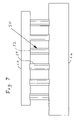
- FIG. 7 illustrates the use of thin copper wire forming the core of more robust and more electrically conductive solder columns, in accordance with the invention.
- FIG. 8 shows higher temperature solder columns attached directly to a silicon die or wafer, in accordance with the invention.
- FIG. 9 shows lower temperature solder attached either to column tips or directly to the substrate, or both, in accordance with the invention.
- FIG. 10 shows the robust interconnect made between silicon chip and organic substrate with a lower temperature solder, in accordance with the invention.
- FIG. 11 shows how an opaque underfill prevents the formation of an optical pathway from the base of a chip to the substrate, as in the prior art.
- FIG. 12 shows how, in accordance with the invention, robust interconnects provide space for both optical and electrical communication.
- mold cavities for solder bumps that are fabricated by etching chemically or by using a laser, are generally hemispherical in shape.
- the present inventors have determined that the transferred bumps may be molded to a shape which can be chosen to provide an increase in the fatigue resistance of the final solder joint.
- the solder has been molded into structures in the shape of columns 30 , as a result of mold cavities that are preferably cylindrical in shape.
- the greater height to width aspect ratio of the columns is able to accommodate the mechanical stresses since the columns 30 are able to bend slightly, which is especially desirable for the columns around the perimeter due to the greater DNP.
- the height to width ratio will be referred to herein as aspect ratio, and in accordance with the invention, will have a value greater than one, as illustrated in FIG. 3 , where the aspect ratio is modestly greater than one.
- the material of the substrate 22 which has in the past been limited by differences in CTE from that of the chip 20 , may be comprised of a broader range of materials.
- the improved solder interconnects of the present invention can be used to make electrical connections to metallic electrical connection surfaces on substrates formed of organic materials, such as polymers having optimized electrical, mechanical and thermal properties.
- Current polymeric substrates are highly filled with inorganic particles to reduce CTE. The filler particles have negative effects on the electrical and mechanical properties of the polymeric materials.
- solder used to form the improved interconnects may be any one of those well known in the art. Standard eutectic PbSn solders having a melting temperature of 183° C. may be used. Tin-rich lead-free solders having a melting point of 217° C.-240° C. are also candidates. High lead solders with ninety five to ninety seven percent lead and the remainder substantially of tin, with a melting point of 320° C. may also be used.
- FIG. 4 illustrates an embodiment of the invention similar to FIG. 3 , except that the columns 30 are attached to the substrate 22 and an underfill layer is in place between the chip 20 and the substrate 22 .
- the present invention can be used to eliminate the requirement for the underfill layer, in some applications, it may nevertheless be desirable to include an underfill layer 28 , and the principles of the invention do not exclude the used of an underfill layer.
- FIG. 5 illustrates an embodiment of the invention wherein columns 40 are formed of solder and have a high aspect ratio.
- the aspect ratio may also have a much greater value, such as 2:1 to 4:1, or even 10:1.
- IMS provides the option of incorporating filler particles into the molten solder to give a composite material column 40 A of increased mechanical strength.
- the composition of the filler particles may include metallic materials, graphitic carbon, ceramic powders and high temperature stable polymeric materials.
- solder bumps solder paste screening, solder evaporation, and solder plating
- solder paste screening solder paste screening
- solder evaporation solder plating
- the final shape of the solder bumps is nearly spherical, as the final step in each case is a solder reflow to eliminate the irregular shape resulting from screening, evaporation through a mask, or plating in openings in a photoresist.
- Forming a composite solder joint is also difficult with any of these prior art processes because they do not lend themselves to uniform mixing in of a non-solder material.
- the solder is handled in the molten state, and mixing in of a particulate material for reinforcement of the joints can be done in the molten state, to produce the composite columns 40 A shown in FIG. 6 .
- columns 50 formed with a internal copper wire core 52 , or another conductive metal wire such as nickel, tantalum, tungsten, or ruthenium, surrounded by solder 54 , are utilized.
- Columns 50 are formed by placing the thin copper or other metal wire in the solder mold cavities before solder is injected.
- These copper cores 52 act as a “reinforcement member” for the solder that is then cast around the wire.
- the copper cores 52 also improve the electrical properties of the interconnect.
- solder connections resulting in improved interconnects are usually produced with a solder hierarchy.
- the molded solder columns whether of the type 30 of FIG. 3 (or 40 of FIG. 5 , 40 A of FIG. 6 or 50 of FIG. 7 (with a conductive metal core)), are made of or with a higher temperature solder and are transferred at the elevated temperature to the entire wafer or individual silicon die to provide the greater standoff height.
- FIG. 9 shows that a lower temperature solder 70 may be applied to either the substrate or the ends of the columns, and while generally not preferred, to both the substrate and the tips of the columns.
- FIG. 11 and FIG. 12 illustrate another key advantage of robust interconnects produced by the invention.
- newer schemes involving optical and electrical interconnections in a hybrid package become more generally available, there will be a need to provide an optical pathway from the optical diodes, or other optical devices that are interspersed with electrically active pads at the base of the silicon die or chip 20 A to the organic substrate 22 A containing other optical components.
- the opaque underfill layer 28 prohibits such an optical pathway.
- the robust interconnects in accordance with the invention may eliminate the need for underfill. This allows such hybrid packages, by virtue of the fact that there is an unimpeded pathway, to have optical communication 100 between the base of the silicon chip 20 C and the substrate 22 C. This permits many additional advances in combining the attributes, for example, of electrical connections, provided by interconnect columns 30 for power, and optical connections between optical components 102 and 104 , along pathways 106 for signal, in the same package.
- the complicated assembly and difficulty in reworking flip chips with underfill has limited the use of flip chips to single chip packages or to multi-chip packages on ceramic substrates for which the CTE mismatch is tolerable without underfill.
- the improved solder interconnect technology of the present invention enables a much wider use of flip chips on plastic modules for the fastest growing markets for semiconductors.
- the improved solder interconnects can also be used with underfill, however.
- the increased standoff provided by cylindrical solder interconnects of aspect ratio of even as small as 1.5:1 will simplify the underfill process and increase the fatigue life of underfilled chips.
- a preferred structure for improved flip chip interconnects may have cylindrical solder columns of diameter of 25-150 microns, preferably 50-100 microns.
- the interconnects may be 100-600 microns long, with an aspect ratio of length to diameter of 1.5:1-10:1, with a preferred range of 2:1 to 4:1.
- the method of fabrication of the interconnects can be described as follows.
- a rectangular or square mold plate is patterned with an array of preferably cylindrical cavities.
- the mold plate can be of borosilicate glass, or be a composite of a laser machined polymer layer and glass, as disclosed in U.S. patent application Ser. No. 11/168,182, entitled Composite Solder Transfer Moldplate Structure and Method of Making Same, which is assigned to the same assigned as the present invention and is incorporated herein in its entirety.
- the moldplate can be of a size to encompass a 200 mm or 300 mm wafer pattern such that the array of cavities exactly matches the array of electrical connection pads on the wafer to which the flip chip interconnects are to be joined.
- the cavities in the mold plate are fabricated by wet etching or laser etching by processes known in the art.
- the cavities have the dimensions of the flip chip interconnects, i.e. 50-150 microns diameter and 100-600 microns deep.
- the cavity diameter is preferably slightly wider at the top than at the bottom; for example, approximately five percent to twenty percent larger in diameter, to facilitate withdrawal of the interconnects from the mold.
- the molten solder is transferred into the cavities containing the wires using the injection molded solder tool that has been described in previous U.S. Pat. No. 6,056,191.
- the mold plate is aligned to the wafer, clamped and transferred into a solder reflow oven.
- the solder preferentially wets the pads on the wafer, thereby transferring the solder column containing the copper wire to the wafer.
- the solder cools and the mold plate is separated from the wafer, leaving the desired solder interconnects on the wafer, and providing the empty mold plate for reuse.
- the chips are ready for package bond and assembly. Because the improved solder interconnects of this example have a height to diameter aspect ratio greater than one, if desired, underfilling of following flip chip bonding is facilitated in comparison to packages using conventional spherical solder bumps.
- Another preferred structure for improved flip chip interconnects is one in which a copper wire of diameter 25-100 microns is embedded in a solder column of diameter 50-150 microns.
- the interconnects may be 100-600 microns long, with an aspect ratio of length to diameter of 1.5:1-10:1, with a preferred range of 2:1 to 4:1.
- the method of fabrication of the interconnects can be described as follows.
- a rectangular or square mold plate is patterned with an array of preferably cylindrical cavities.
- the mold plate can be of borosilicate glass or be a composite of polymer and glass, as disclosed in U.S. patent application Ser. No. 11/168,182, entitled Composite Solder Transfer Moldplate Structure and Method of Making Same, which is incorporated herein in its entirety.
- the moldplate is of a size to encompass a 200 mm or 300 mm wafer pattern such that the array of cavities exactly matches the array of electrical connection pads on the wafer to which the flip chip interconnects are to be joined.
- the cavities in the mold plate are fabricated by wet etching or laser etching by processes known in the art.
- the cavities have the dimensions of the flip chip interconnects, i.e. 50-150 microns diameter and 100-600 microns deep.
- the cavity diameter is preferably slightly wider at the top than at the bottom; for example, approximately five percent to twenty percent larger in diameter, to facilitate withdrawal of the interconnects from the mold.
- the copper wire is thinly coated by electroplating with solder-wettable metals such as nickel and gold.
- solder-wettable metals such as nickel and gold.
- a single copper wire is placed in each cavity in the mold plate.
- Several methods can be used to facilitate transfer of the copper wire to the cavities in the mold plate.
- a wire bonding tool is used to feed a controlled length of the wire into each cavity and each wire can be cut by flame-off, a process well known in the art wherein the wire is melted by a high temperature flame.
- the length of wire must be no longer than the depth of the cavities or preferably one percent to two percent shorter.
- a thin glass plate or polymer film is fabricated with through-holes of diameter slightly larger than the copper wire in an array exactly matching the array of cavities in the mold plate.
- This plate is aligned with the mold plate and clamped together with it.
- the copper wire is then precut into lengths slightly less than the depth of the cavities and a collection of these wires is agitated over the openings until a single wire falls into each of the cavities below.
- a programmable pick and place tool is used to insert a single length of precut and electroplated wire in each cavity in the mold plate.
- the molten solder is transferred into the cavities containing the wires using the injection molded solder tool that has been described in previous U.S. Pat. No. 6,056,191.
- the mold plate is aligned to the wafer, clamped and transferred into a solder reflow oven.
- the solder preferentially wets the pads on the wafer, thereby transferring the solder column containing the copper wire to the wafer.
- the solder cools and the mold plate is separated from the wafer, leaving the desired composite solder/copper interconnects on the wafer, and providing the empty mold plate for reuse.
- solder interconnects of this example provide superior mechanical and electrical properties to the resultant packages in comparison to those resulting from the use of conventional spherical solder bumps.
Abstract
Improved interconnects are produced by injection molded solder which fills mold arrays with molten solder so that columns that have much greater height to width aspect ratios greater than one are formed, rather than conventional flip chip bumps. The columns may have filler particles or reinforcing conductors therein. In the interconnect structures produced, the cost and time of a subsequent underfill step is reduced or avoided. The problem of incompatibility with optical interconnects between chips because underfills require high loading of silica fillers which scatter light, is solved, thus allowing flip chips to incorporate optical interconnects.
Description
This invention relates to the field of solder interconnects formed between circuit devices and substrates forming the next layer of electrical interconnect. More specifically, the invention relates to improvements in injection molded solder technologies used to form solder bump interconnections, generally on silicon wafers.
Semiconductor chips are commonly connected to other circuitry using solder bumps having a diameter of about 100 microns. These solder joints suffer thermal fatigue failures because of the difference in coefficient of thermal expansion (CTE) between the silicon and the chip carriers to which they are attached. Using the injection molded solder (IMS) technique, solder interconnects can be fabricated on semiconductor chips or chip carriers with controlled shape and composition to increase the fatigue life of the joints. Thus, this invention pertains to improvements of solder interconnections for better electrical performance and/or increased mechanical robustness and the fabrication process of same using IMS.
IMS is a relatively new process with many applications, primarily suited for low-cost solder bumping of semiconductor wafers. In IMS, a scanning head dispenses molten solder through a linear slot in the head over a mold plate to fill cavities therein with molten solder.
After the scan, the solder in the cavities is solidified and then the mold plate is aligned to and placed in contact with a wafer (or die or semiconductor chip) by an appropriate fixture. This assembly is then heated to facilitate reflow and transfer of the solder from the mold plate cavities to metallized pads on the wafer. After cooling and separating the wafer and mold plate, the wafer has been bumped with an array of solder preforms typically used for flip chip applications.
While the technology disclosed in U.S. Pat. No. 6,056,191, assigned to the assignee of the present invention, and entitled “Method and Apparatus for Forming Solder Bumps” represents a major advance in the art, it typically produces spherical solder joints that exhibit several problems. First, the spherical solder joints have limited fatigue life due to a difference in coefficient of thermal expansion between the silicon die and the substrate, often an organic material. To address this CTE mismatch, an additional underfill material is needed between the silicon die and substrate to reduce the mechanical stresses on the solder bumps. As the level of integration in silicon continues to increase, the number and density of solder interconnections also must increase, driving a reduction in size of the spherical solder joints and making it difficult or impossible for underfill to be used. Second, silicon chip sizes are increasing, which also limits the ability of underfills to reinforce conventional spherical solder interconnects. Third, power requirements for silicon devices are increasing, particularly for microprocessor chips; and conventional solder interconnects may not be able to withstand the higher currents needed to supply that power. Finally, as newer interconnect structures are developed such as optical interconnects, the underfill material itself will present a problem, since optical communication between the die and substrate is prevented due to the opaque nature of the material.
The first problem is shown in FIG. 1 , wherein a die or chip 20 (typically an integrated circuit silicon chip) is electrically interconnected to a substrate 22 by a series of solder bumps 24, as is well known in the art. The typically small height to width aspect ratio (<1) of standard flip chip bumps makes the solder prone to mechanical stresses, which are greatest at the plane represented by arrows 26, as the chip power and temperature varies over its life. This CTE mismatch caused problem is aggravated as chips get larger and thus the DNP (distance to neutral point) is increased. Without underfill, interconnect failures happen at unacceptably short lifetimes.
It is therefore an object of the present invention to provide improved solder interconnects and to a method for providing such interconnects.
It is another object of the invention to provide solder interconnects with greater standoff between chip and substrate to facilitate underfill reinforcement of the interconnects.
It is another object of the invention to provide solder interconnects of improved current carrying capacity.
It is another object of the invention to provide interconnections that are sufficiently mechanically robust that they can be used without the need to place optically blocking layers between the chip and substrate.
In accordance with the invention, a method for connecting an electrical device having first electrical connection surfaces to a substrate having corresponding second electrical connection surfaces, comprises forming a plurality of columns at least partially of solder so as to be electrically connected to one of the first surfaces and the second surfaces so that electrical connections are made to first ends of the columns; and forming electrical connections between the other of the first surfaces and second surfaces and second ends of the respective columns. The columns have an aspect ratio greater than one, such as between 1.5 and ten. The columns may be formed by injection molded soldering.
The columns may be formed of a first solder with a first melting point temperature, and the method may further comprise soldering the columns to the other of the first surfaces and second surfaces with a second solder having a second melting point temperature lower than the first melting point temperature. The second solder may be applied to at least one of the first surfaces and the second surfaces prior to connecting second ends of the columns to the second surfaces.
An elongate metal conductor of a material other than solder may be placed within the columns. The elongate metal conductor may be formed of a material selected from the group of copper, nickel, tantalum, tungsten, and ruthenium. The conductor may be coated with a solder-wettable metal, which may be selected from the group of nickel, gold and silver, or combinations thereof. The coating may be formed by electroplating.
The columns may be formed in a mold. The conductors may be placed in cavities of the mold prior to injecting solder into the cavities.
The placing of the conductors may comprise feeding a controlled length of the conductor into the cavities by using a wire bonding tool; and cutting an end of the conductor so that the conductor fits within the cavity.
The placing of the conductors may comprise aligning, with an array of cavities in the mold plate, an array of through-holes in a plate, the through-holes being slightly larger in diameter than the conductors; removably fastening the plate to the mold plate; placing conductors in the vicinity of the through-holes; and agitating the conductors over the through-holes until a respective conductor moves into each of the cavities. The placing may comprise using a programmable pick and place tool to insert a conductor into the cavities.
The solder of the columns may have filler particles therein. The filler particles may be mixed with the solder when the solder is in a molten state, prior to forming the columns. The particles may have a composition of metal, graphite, ceramic or a high temperature polymer.
The electrical device is generally a semiconductor chip. The substrate may be any conventional material or may be formed of an organic material. An underfill layer may be provided between the electrical device and the substrate.
The invention is also directed to an article of manufacture, comprising an electrical device having first electrical connection surfaces; a substrate having corresponding second electrical connection surfaces, and a plurality of columns at least partially of solder electrically connected to one of the first surfaces and the second surfaces so that electrical connections are made to first ends of the columns; and so that there are electrical connections between the other of the first surfaces and second surfaces and second ends of the respective columns. The columns may have an aspect ratio greater than one, such as between 1.5 and ten. The columns may be formed of injection molded solder. The columns may be formed of a first solder with a first melting point temperature, and the article may further comprise a second solder having a second melting point temperature lower than the first melting point temperature for electrically connecting the columns to the other of the first surfaces and second surfaces. The second solder may be disposed on at least one of the first surfaces and the second surfaces prior to connecting second ends of the columns to the second surfaces.
An elongate metal conductor of a material other than solder may be disposed within the columns. The elongate metal conductor may be of a material selected from the group of copper, nickel, tantalum, tungsten, and ruthenium. The conductor may have a solder-wettable metal coating. The solder wettable metal may be selected from the group of nickel, gold, silver, tin and combinations thereof. The coating may be an electroplated coating.
The solder may have filler particles therein. The particles may be comprised of metal, graphite, ceramic or a high temperature polymer.
The electrical device is generally a semiconductor chip. The substrate may be comprised a conventional material or of an organic material.
The article in accordance with the invention may further comprise a first electro-optical device having a portion disposed on a surface of the electrical device; and a second electro-optical device having a portion disposed on a surface the substrate; the first electro-optical device and the second electro-optical device being in facing relationship so as to allow transmission of light between the first electro-optical device and the second electro-optical device. The first electro-optical device and the second electro-optical device may be disposed between a plurality of the columns.
There may be no underfill material between the first electro-optical device and the second electro-optical device. In certain applications, an underfill layer may be disposed between the electrical device and the substrate.
The invention is also directed to an electrical interconnect device comprising an injection molded solder column having a diameter of between 25 microns and 150 microns and an aspect ratio of greater than one. The aspect ratio may be between 1.5 and ten. A reinforcing conductor may be disposed within the column. Filler particles may be disposed within the columns.
These and other aspects, features, and advantages of the present invention will become apparent upon further consideration of the following detailed description of the invention when read in conjunction with the drawing figures, which are all enlarged cross-sectional views, wherein:
In general, mold cavities for solder bumps that are fabricated by etching chemically or by using a laser, are generally hemispherical in shape. However, the present inventors have determined that the transferred bumps may be molded to a shape which can be chosen to provide an increase in the fatigue resistance of the final solder joint.
In FIG. 3 , the solder has been molded into structures in the shape of columns 30, as a result of mold cavities that are preferably cylindrical in shape. The greater height to width aspect ratio of the columns, as compared to the prior art generally spherical shape, is able to accommodate the mechanical stresses since the columns 30 are able to bend slightly, which is especially desirable for the columns around the perimeter due to the greater DNP. In general, the height to width ratio, as noted above, will be referred to herein as aspect ratio, and in accordance with the invention, will have a value greater than one, as illustrated in FIG. 3 , where the aspect ratio is modestly greater than one.
Advantageously, the material of the substrate 22, which has in the past been limited by differences in CTE from that of the chip 20, may be comprised of a broader range of materials. For example, the improved solder interconnects of the present invention can be used to make electrical connections to metallic electrical connection surfaces on substrates formed of organic materials, such as polymers having optimized electrical, mechanical and thermal properties. Current polymeric substrates are highly filled with inorganic particles to reduce CTE. The filler particles have negative effects on the electrical and mechanical properties of the polymeric materials.
The solder used to form the improved interconnects may be any one of those well known in the art. Standard eutectic PbSn solders having a melting temperature of 183° C. may be used. Tin-rich lead-free solders having a melting point of 217° C.-240° C. are also candidates. High lead solders with ninety five to ninety seven percent lead and the remainder substantially of tin, with a melting point of 320° C. may also be used.
The manner in which the electrical connections are made using, in general, more than one solder, is discussed below.
Referring to FIG. 6 , IMS provides the option of incorporating filler particles into the molten solder to give a composite material column 40A of increased mechanical strength. The composition of the filler particles may include metallic materials, graphitic carbon, ceramic powders and high temperature stable polymeric materials.
The ability to form solder columns and optionally add reinforcing particles to the solder is in sharp contrast to the conventional processes for fabricating solder bumps (solder paste screening, solder evaporation, and solder plating) that do not provide any flexibility in solder bump shape and composition. In all three of the prior art processes, the final shape of the solder bumps is nearly spherical, as the final step in each case is a solder reflow to eliminate the irregular shape resulting from screening, evaporation through a mask, or plating in openings in a photoresist. Forming a composite solder joint is also difficult with any of these prior art processes because they do not lend themselves to uniform mixing in of a non-solder material.
In accordance with the invention, by using IMS, the solder is handled in the molten state, and mixing in of a particulate material for reinforcement of the joints can be done in the molten state, to produce the composite columns 40A shown in FIG. 6 .
In FIG. 7 , in an alternative embodiment of the invention, columns 50, formed with a internal copper wire core 52, or another conductive metal wire such as nickel, tantalum, tungsten, or ruthenium, surrounded by solder 54, are utilized. Columns 50 are formed by placing the thin copper or other metal wire in the solder mold cavities before solder is injected. These copper cores 52 act as a “reinforcement member” for the solder that is then cast around the wire. The copper cores 52 also improve the electrical properties of the interconnect.
As shown in FIG. 8 , solder connections resulting in improved interconnects are usually produced with a solder hierarchy. Thus the molded solder columns, whether of the type 30 of FIG. 3 (or 40 of FIG. 5 , 40A of FIG. 6 or 50 of FIG. 7 (with a conductive metal core)), are made of or with a higher temperature solder and are transferred at the elevated temperature to the entire wafer or individual silicon die to provide the greater standoff height.
As shown in FIG. 10 , when the final solder joint to connect the die to the substrate is made by reflowing, this can be done by melting only the lower melting point solder 70, without remelting the solder of the columns 30.
In FIG. 12 , the robust interconnects in accordance with the invention may eliminate the need for underfill. This allows such hybrid packages, by virtue of the fact that there is an unimpeded pathway, to have optical communication 100 between the base of the silicon chip 20C and the substrate 22C. This permits many additional advances in combining the attributes, for example, of electrical connections, provided by interconnect columns 30 for power, and optical connections between optical components 102 and 104, along pathways 106 for signal, in the same package.
Eliminating the need for underfill by fabricating robust solder interconnects, as disclosed herein, considerably simplifies the assembly process and increase the applicability of bumped chips, i.e. flip chips. In the prior art, the complicated assembly and difficulty in reworking flip chips with underfill has limited the use of flip chips to single chip packages or to multi-chip packages on ceramic substrates for which the CTE mismatch is tolerable without underfill. The improved solder interconnect technology of the present invention enables a much wider use of flip chips on plastic modules for the fastest growing markets for semiconductors. The improved solder interconnects can also be used with underfill, however. The increased standoff provided by cylindrical solder interconnects of aspect ratio of even as small as 1.5:1 will simplify the underfill process and increase the fatigue life of underfilled chips.
A preferred structure for improved flip chip interconnects may have cylindrical solder columns of diameter of 25-150 microns, preferably 50-100 microns. The interconnects may be 100-600 microns long, with an aspect ratio of length to diameter of 1.5:1-10:1, with a preferred range of 2:1 to 4:1. The method of fabrication of the interconnects can be described as follows.
A rectangular or square mold plate is patterned with an array of preferably cylindrical cavities. The mold plate can be of borosilicate glass, or be a composite of a laser machined polymer layer and glass, as disclosed in U.S. patent application Ser. No. 11/168,182, entitled Composite Solder Transfer Moldplate Structure and Method of Making Same, which is assigned to the same assigned as the present invention and is incorporated herein in its entirety. Further, the moldplate can be of a size to encompass a 200 mm or 300 mm wafer pattern such that the array of cavities exactly matches the array of electrical connection pads on the wafer to which the flip chip interconnects are to be joined. The cavities in the mold plate are fabricated by wet etching or laser etching by processes known in the art. The cavities have the dimensions of the flip chip interconnects, i.e. 50-150 microns diameter and 100-600 microns deep. The cavity diameter is preferably slightly wider at the top than at the bottom; for example, approximately five percent to twenty percent larger in diameter, to facilitate withdrawal of the interconnects from the mold.
The molten solder is transferred into the cavities containing the wires using the injection molded solder tool that has been described in previous U.S. Pat. No. 6,056,191. Following inspection of the filled mold plate to be certain that each cavity is filled with solder, the mold plate is aligned to the wafer, clamped and transferred into a solder reflow oven. As previously disclosed in U.S. Pat. No. 6,056,191, the solder preferentially wets the pads on the wafer, thereby transferring the solder column containing the copper wire to the wafer. After exiting the reflow oven, the solder cools and the mold plate is separated from the wafer, leaving the desired solder interconnects on the wafer, and providing the empty mold plate for reuse.
Following wafer test, inspection and dicing, the chips are ready for package bond and assembly. Because the improved solder interconnects of this example have a height to diameter aspect ratio greater than one, if desired, underfilling of following flip chip bonding is facilitated in comparison to packages using conventional spherical solder bumps.
Another preferred structure for improved flip chip interconnects is one in which a copper wire of diameter 25-100 microns is embedded in a solder column of diameter 50-150 microns. The interconnects may be 100-600 microns long, with an aspect ratio of length to diameter of 1.5:1-10:1, with a preferred range of 2:1 to 4:1. The method of fabrication of the interconnects can be described as follows.
A rectangular or square mold plate is patterned with an array of preferably cylindrical cavities. The mold plate can be of borosilicate glass or be a composite of polymer and glass, as disclosed in U.S. patent application Ser. No. 11/168,182, entitled Composite Solder Transfer Moldplate Structure and Method of Making Same, which is incorporated herein in its entirety. Further, the moldplate is of a size to encompass a 200 mm or 300 mm wafer pattern such that the array of cavities exactly matches the array of electrical connection pads on the wafer to which the flip chip interconnects are to be joined. The cavities in the mold plate are fabricated by wet etching or laser etching by processes known in the art. The cavities have the dimensions of the flip chip interconnects, i.e. 50-150 microns diameter and 100-600 microns deep. The cavity diameter is preferably slightly wider at the top than at the bottom; for example, approximately five percent to twenty percent larger in diameter, to facilitate withdrawal of the interconnects from the mold.
The copper wire is thinly coated by electroplating with solder-wettable metals such as nickel and gold. A single copper wire is placed in each cavity in the mold plate. Several methods can be used to facilitate transfer of the copper wire to the cavities in the mold plate. In the first method, a wire bonding tool is used to feed a controlled length of the wire into each cavity and each wire can be cut by flame-off, a process well known in the art wherein the wire is melted by a high temperature flame. The length of wire must be no longer than the depth of the cavities or preferably one percent to two percent shorter. Alternatively, in the second method, a thin glass plate or polymer film is fabricated with through-holes of diameter slightly larger than the copper wire in an array exactly matching the array of cavities in the mold plate. This plate is aligned with the mold plate and clamped together with it. The copper wire is then precut into lengths slightly less than the depth of the cavities and a collection of these wires is agitated over the openings until a single wire falls into each of the cavities below. In a third method, a programmable pick and place tool is used to insert a single length of precut and electroplated wire in each cavity in the mold plate.
Once the copper wires are in place, the molten solder is transferred into the cavities containing the wires using the injection molded solder tool that has been described in previous U.S. Pat. No. 6,056,191. Following inspection of the filled mold plate to be certain that each cavity is filled with solder and copper wire, the mold plate is aligned to the wafer, clamped and transferred into a solder reflow oven. As previously disclosed in U.S. Pat. No. 6,056,191, the solder preferentially wets the pads on the wafer, thereby transferring the solder column containing the copper wire to the wafer. After exiting the reflow oven, the solder cools and the mold plate is separated from the wafer, leaving the desired composite solder/copper interconnects on the wafer, and providing the empty mold plate for reuse.
Following wafer test, inspection and dicing, the individual chips are ready for package bond and assembly. The improved solder interconnects of this example provide superior mechanical and electrical properties to the resultant packages in comparison to those resulting from the use of conventional spherical solder bumps.
Variations described for the present invention can be realized in any combination desirable for each particular application. Thus particular limitations, and/or embodiment enhancements described herein, which may have particular advantages to the particular application need not be used for all applications. Also, it should be realized that not all limitations need be implemented in methods, systems and/or apparatus including one or more concepts of the present invention.
The table below indicates the characteristics and advantages of some of the various combinations of elements that may be assembled in accordance with the principles of the invention.
| TABLE 1 |
| Matrix of Improved Interconnect Combinations |
| Column Type | Modest Aspect | High Aspect | ||
| Ratio (1.5-2.0) | Ratio (>2.0) | |||
| Interconnects | Interconnects | |||
| with Underfill | with Partial or | |||
| No Underfill | ||||
| Plain solder | Enables | Enables use of | ||
| underfill for | partial | |||
| dense I/O arrays | underfill; for | |||
| electrical and | ||||
| optical I/O | ||||
| Particle-filled | Improves | Enables | ||
| solder | interconnect | elimination of | ||
| robustness for | underfill; for | |||
| mechanically | electrical and | |||
| stressed | optical I/O | |||
| packages with | (input/output) | |||
| large chips | ||||
| Copper Core + | Interconnects | Interconnects | ||
| Solder | for lowest | for optimal | ||
| electrical | electrical and | |||
| resistance and | optical I/O | |||
| improved package | ||||
| robustness | ||||
It is noted that the foregoing has outlined some of the more pertinent objects and embodiments of the present invention. The concepts of this invention may be used for many applications. Thus, although the description is made for particular arrangements and methods, the intent and concept of the invention is suitable and applicable to other arrangements and applications. It will be clear to those skilled in the art that other modifications to the disclosed embodiments can be effected without departing from the spirit and scope of the invention. The described embodiments ought to be construed to be merely illustrative of some of the more prominent features and applications of the invention. Other beneficial results can be realized by applying the disclosed invention in a different manner or modifying the invention in ways known to those familiar with the art. Thus, it should be understood that the embodiments has been provided as an example and not as a limitation. The scope of the invention is defined by the appended claims.
Claims (13)
1. A method for connecting an electrical device having first electrical connection surfaces to a substrate having corresponding second electrical connection surfaces, comprising:
forming a plurality of columns at least partially of solder so as to be electrically connected to one of said first electrical connection surfaces and said second electrical connection surfaces; wherein electrical connections are made between first ends of said plurality of columns and said first electrical connection surfaces;
forming electrical connections between said second electrical connection surfaces and second ends of respective ones of said plurality of columns;
mixing particles with solder when the solder is in a molten state;
forming said columns in cavities of a mold plate by injection molded soldering of said solder, said columns having an aspect ratio of between 1.5 and ten;
coating, by electroplating, elongate metal conductors of a material other than solder with a solder-wettable metal;
placing said metal conductors within respective columns in said mold plate prior to injecting solder into said cavities;
aligning, with an array of cavities in the mold plate, an array of through-holes in a plate, the through-holes being slightly larger in diameter than the conductors;
removably fastening the plate to the mold plate;
placing conductors in the vicinity of the through-holes;
agitating the conductors over the through-holes until a respective conductor moves into each of the cavities;
providing first optical components on said electrical device and second optical components on said substrate, said first optical components and said second optical components being positioned with respect to one another so that there is a respective optical path between each one of said first optical components and a respective one of said second optical components, said optical paths having no underfill material; wherein:
said columns are formed of a first solder with a first melting point temperature, further comprising soldering said columns to the other of said first surfaces and second surfaces with a second solder having a second melting point temperature lower than said first melting point temperature; and
said second solder is applied to at least one of said first electrical connection surfaces and said second electrical connection surfaces prior to connecting second ends of said columns to said first surface and said second surfaces.
2. A method as recited in claim 1 , wherein said elongate metal conductor is formed of a material selected from the group consisting of copper, nickel, tantalum, tungsten, and ruthenium.
3. A method as recited in claim 1 , wherein said solder wettable metal is selected from the group consisting of nickel, gold and silver, or combinations thereof.
4. A method as recited in claim 1 , wherein said particles have a composition of metal, graphite, ceramic or high temperature polymer.
5. A method as recited in claim 1 , wherein said electrical device is a semiconductor chip.
6. A method as recited in claim 1 , wherein said substrate is formed of an organic material.
7. A method as recited in claim 1 , wherein said optical pathways are located among said plurality of columns.
8. A method for connecting an electrical device having first electrical connection surfaces to a substrate having corresponding second electrical connection surfaces, comprising:
forming a plurality of columns at least partially of solder so as to be electrically connected to one of said first electrical connection surfaces and said second electrical connection surfaces; wherein electrical connections are made between first ends of said plurality of columns and said first electrical connection surfaces;
forming electrical connections between said second electrical connection surfaces and second ends of respective ones of said plurality of columns;
mixing particles with solder when the solder is in a molten state;
forming said columns in cavities of a mold plate by injection molded soldering of said solder, said columns having an aspect ratio of between 1.5 and ten;
coating, by electroplating, elongate metal conductors of a material other than solder with a solder-wettable metal;
placing said metal conductors within respective columns in said mold plate prior to injecting solder into said cavities;
providing first optical components on said electrical device and second optical components on said substrate, said first optical components and said second optical components being positioned with respect to one another so that there is a respective optical path between each one of said first optical components and a respective one of said second optical components, said optical pathways being located among said plurality of columns; and
using a pick and place tool to place an elongate metal conductor of a material other than solder within said columns in said mold prior to injecting solder into said cavities; wherein:
said columns are formed of a first solder with a first melting point temperature, further comprising soldering said columns to the other of said first surfaces and second surfaces with a second solder having a second melting point temperature lower than said first melting point temperature; and
said second solder is applied to at least one of said first electrical connection surfaces and said second electrical connection surfaces prior to connecting second ends of said columns to said first surface and said second surfaces.
9. A method as recited in claim 8 , wherein said elongate metal conductor is formed of a material selected from the group consisting of copper, nickel, tantalum, tungsten, and ruthenium.
10. A method as recited in claim 8 , wherein said solder wettable metal is selected from the group consisting of nickel, gold and silver, or combinations thereof.
11. A method as recited in claim 8 , wherein said particles have a composition of metal, graphite, ceramic or high temperature polymer.
12. A method as recited in claim 8 , wherein said electrical device is a semiconductor chip.
13. A method as recited in claim 8 , wherein said substrate is formed of an organic material.
Priority Applications (2)
| Application Number | Priority Date | Filing Date | Title |
|---|---|---|---|
| US11/005,557 US7523852B2 (en) | 2004-12-05 | 2004-12-05 | Solder interconnect structure and method using injection molded solder |
| CNB2005101253107A CN100513037C (en) | 2004-12-05 | 2005-11-15 | Solder interconnect structure and method using injection molded solder |
Applications Claiming Priority (1)
| Application Number | Priority Date | Filing Date | Title |
|---|---|---|---|
| US11/005,557 US7523852B2 (en) | 2004-12-05 | 2004-12-05 | Solder interconnect structure and method using injection molded solder |
Publications (2)
| Publication Number | Publication Date |
|---|---|
| US20060118604A1 US20060118604A1 (en) | 2006-06-08 |
| US7523852B2 true US7523852B2 (en) | 2009-04-28 |
Family
ID=36573081
Family Applications (1)
| Application Number | Title | Priority Date | Filing Date |
|---|---|---|---|
| US11/005,557 Expired - Fee Related US7523852B2 (en) | 2004-12-05 | 2004-12-05 | Solder interconnect structure and method using injection molded solder |
Country Status (2)
| Country | Link |
|---|---|
| US (1) | US7523852B2 (en) |
| CN (1) | CN100513037C (en) |
Cited By (6)
| Publication number | Priority date | Publication date | Assignee | Title |
|---|---|---|---|---|
| US20070125571A1 (en) * | 2005-12-02 | 2007-06-07 | Honeywell International Inc. | Column grid array using compliant core |
| US20100008621A1 (en) * | 2008-01-24 | 2010-01-14 | Nitto Denko Corporation | Manufacturing method of opto-electric hybrid board and opto-electric hybrid board obtained thereby |
| US20140026394A1 (en) * | 2012-07-25 | 2014-01-30 | International Business Machines Corporation | Electro-optical assembly for silicon photonic chip and electro-optical carrier |
| US9343420B2 (en) | 2014-02-14 | 2016-05-17 | Globalfoundries Inc. | Universal solder joints for 3D packaging |
| US10477698B1 (en) * | 2019-04-17 | 2019-11-12 | Topline Corporation | Solder columns and methods for making same |
| US10937752B1 (en) | 2020-08-03 | 2021-03-02 | Topline Corporation | Lead free solder columns and methods for making same |
Families Citing this family (13)
| Publication number | Priority date | Publication date | Assignee | Title |
|---|---|---|---|---|
| US20090065555A1 (en) * | 2007-09-12 | 2009-03-12 | Stephen Leslie Buchwalter | Electrical interconnect forming method |
| US20090200663A1 (en) | 2008-02-11 | 2009-08-13 | Daubenspeck Timothy H | Polymer and solder pillars for connecting chip and carrier |
| CN102157481B (en) * | 2011-03-31 | 2012-07-04 | 无锡中微高科电子有限公司 | Stress strain welding column for integrated circuit packaging |
| US9128289B2 (en) | 2012-12-28 | 2015-09-08 | Pixtronix, Inc. | Display apparatus incorporating high-aspect ratio electrical interconnects |
| US20140071142A1 (en) * | 2012-09-13 | 2014-03-13 | Pixtronix, Inc. | Display apparatus incorporating vertically oriented electrical interconnects |
| WO2015194473A1 (en) * | 2014-06-20 | 2015-12-23 | Jsr株式会社 | Method for producing solder electrode, method for producing laminate, laminate and electronic component |
| KR102344790B1 (en) | 2014-08-29 | 2021-12-30 | 닛데쓰마이크로메탈가부시키가이샤 | CYLINDRICAL FORMED BODY FOR Cu PILLARS FOR SEMICONDUCTOR CONNECTION |
| CN106129032A (en) * | 2016-08-14 | 2016-11-16 | 天津大学 | Column soldered ball redistribution encapsulating structure for VLSI chip |
| CN111162013B (en) * | 2020-01-06 | 2021-08-24 | 亿芯微半导体科技(深圳)有限公司 | Semiconductor packaging structure and manufacturing method of semiconductor package |
| CN111146093B (en) * | 2020-01-06 | 2021-08-24 | 亿芯微半导体科技(深圳)有限公司 | Semiconductor stack packaging structure and preparation method thereof |
| CN111199889B (en) * | 2020-01-10 | 2021-07-16 | 宝德照明集团有限公司 | Semiconductor packaging structure and preparation method thereof |
| CN111192863B (en) * | 2020-01-10 | 2021-07-13 | 广东汉岂工业技术研发有限公司 | Chip stacking and packaging structure and preparation method thereof |
| CN112614821A (en) * | 2020-12-15 | 2021-04-06 | Oppo广东移动通信有限公司 | Packaging structure, preparation method thereof and electronic equipment |
Citations (19)
| Publication number | Priority date | Publication date | Assignee | Title |
|---|---|---|---|---|
| US2922092A (en) * | 1957-05-09 | 1960-01-19 | Westinghouse Electric Corp | Base contact members for semiconductor devices |
| US4642889A (en) * | 1985-04-29 | 1987-02-17 | Amp Incorporated | Compliant interconnection and method therefor |
| US4705205A (en) * | 1983-06-30 | 1987-11-10 | Raychem Corporation | Chip carrier mounting device |
| US4914814A (en) * | 1989-05-04 | 1990-04-10 | International Business Machines Corporation | Process of fabricating a circuit package |
| US5244143A (en) * | 1992-04-16 | 1993-09-14 | International Business Machines Corporation | Apparatus and method for injection molding solder and applications thereof |
| US5349495A (en) * | 1989-06-23 | 1994-09-20 | Vlsi Technology, Inc. | System for securing and electrically connecting a semiconductor chip to a substrate |
| US5476211A (en) * | 1993-11-16 | 1995-12-19 | Form Factor, Inc. | Method of manufacturing electrical contacts, using a sacrificial member |
| US5718367A (en) * | 1995-11-21 | 1998-02-17 | International Business Machines Corporation | Mold transfer apparatus and method |
| US5718361A (en) * | 1995-11-21 | 1998-02-17 | International Business Machines Corporation | Apparatus and method for forming mold for metallic material |
| US5775569A (en) * | 1996-10-31 | 1998-07-07 | Ibm Corporation | Method for building interconnect structures by injection molded solder and structures built |
| US6024274A (en) * | 1996-04-03 | 2000-02-15 | Industrial Technology Research Institute | Method for tape automated bonding to composite bumps |
| US6056191A (en) | 1998-04-30 | 2000-05-02 | International Business Machines Corporation | Method and apparatus for forming solder bumps |
| US6283359B1 (en) * | 1998-04-30 | 2001-09-04 | International Business Machines Corporation | Method for enhancing fatigue life of ball grid arrays |
| US6365973B1 (en) * | 1999-12-07 | 2002-04-02 | Intel Corporation | Filled solder |
| US6406991B2 (en) * | 1999-12-27 | 2002-06-18 | Hoya Corporation | Method of manufacturing a contact element and a multi-layered wiring substrate, and wafer batch contact board |
| US20020179689A1 (en) * | 2000-04-27 | 2002-12-05 | Advanpack Solutions Pte. Ltd. | Pillar connections for semiconductor chips and method of manufacture |
| US20040144834A1 (en) | 2003-01-15 | 2004-07-29 | Shinichi Nomoto | Apparatus and method for aligning and attaching solder columns to a substrate |
| US6815613B2 (en) * | 2000-09-13 | 2004-11-09 | Technologies Ag | Electronic component with external connection elements |
| US6906598B2 (en) * | 2002-12-31 | 2005-06-14 | Mcnc | Three dimensional multimode and optical coupling devices |
Family Cites Families (5)
| Publication number | Priority date | Publication date | Assignee | Title |
|---|---|---|---|---|
| US5591941A (en) * | 1993-10-28 | 1997-01-07 | International Business Machines Corporation | Solder ball interconnected assembly |
| US5762258A (en) * | 1996-07-23 | 1998-06-09 | International Business Machines Corporation | Method of making an electronic package having spacer elements |
| JP2001338947A (en) * | 2000-05-26 | 2001-12-07 | Nec Corp | Flip chip type semiconductor device and its manufacturing method |
| CN1330398A (en) * | 2000-06-16 | 2002-01-09 | 国际商业机器公司 | Tube core level encapsulation and manufacturing method thereof |
| US6276596B1 (en) * | 2000-08-28 | 2001-08-21 | International Business Machines Corporation | Low temperature solder column attach by injection molded solder and structure formed |
-
2004
- 2004-12-05 US US11/005,557 patent/US7523852B2/en not_active Expired - Fee Related
-
2005
- 2005-11-15 CN CNB2005101253107A patent/CN100513037C/en not_active Expired - Fee Related
Patent Citations (19)
| Publication number | Priority date | Publication date | Assignee | Title |
|---|---|---|---|---|
| US2922092A (en) * | 1957-05-09 | 1960-01-19 | Westinghouse Electric Corp | Base contact members for semiconductor devices |
| US4705205A (en) * | 1983-06-30 | 1987-11-10 | Raychem Corporation | Chip carrier mounting device |
| US4642889A (en) * | 1985-04-29 | 1987-02-17 | Amp Incorporated | Compliant interconnection and method therefor |
| US4914814A (en) * | 1989-05-04 | 1990-04-10 | International Business Machines Corporation | Process of fabricating a circuit package |
| US5349495A (en) * | 1989-06-23 | 1994-09-20 | Vlsi Technology, Inc. | System for securing and electrically connecting a semiconductor chip to a substrate |
| US5244143A (en) * | 1992-04-16 | 1993-09-14 | International Business Machines Corporation | Apparatus and method for injection molding solder and applications thereof |
| US5476211A (en) * | 1993-11-16 | 1995-12-19 | Form Factor, Inc. | Method of manufacturing electrical contacts, using a sacrificial member |
| US5718361A (en) * | 1995-11-21 | 1998-02-17 | International Business Machines Corporation | Apparatus and method for forming mold for metallic material |
| US5718367A (en) * | 1995-11-21 | 1998-02-17 | International Business Machines Corporation | Mold transfer apparatus and method |
| US6024274A (en) * | 1996-04-03 | 2000-02-15 | Industrial Technology Research Institute | Method for tape automated bonding to composite bumps |
| US5775569A (en) * | 1996-10-31 | 1998-07-07 | Ibm Corporation | Method for building interconnect structures by injection molded solder and structures built |
| US6056191A (en) | 1998-04-30 | 2000-05-02 | International Business Machines Corporation | Method and apparatus for forming solder bumps |
| US6283359B1 (en) * | 1998-04-30 | 2001-09-04 | International Business Machines Corporation | Method for enhancing fatigue life of ball grid arrays |
| US6365973B1 (en) * | 1999-12-07 | 2002-04-02 | Intel Corporation | Filled solder |
| US6406991B2 (en) * | 1999-12-27 | 2002-06-18 | Hoya Corporation | Method of manufacturing a contact element and a multi-layered wiring substrate, and wafer batch contact board |
| US20020179689A1 (en) * | 2000-04-27 | 2002-12-05 | Advanpack Solutions Pte. Ltd. | Pillar connections for semiconductor chips and method of manufacture |
| US6815613B2 (en) * | 2000-09-13 | 2004-11-09 | Technologies Ag | Electronic component with external connection elements |
| US6906598B2 (en) * | 2002-12-31 | 2005-06-14 | Mcnc | Three dimensional multimode and optical coupling devices |
| US20040144834A1 (en) | 2003-01-15 | 2004-07-29 | Shinichi Nomoto | Apparatus and method for aligning and attaching solder columns to a substrate |
Cited By (10)
| Publication number | Priority date | Publication date | Assignee | Title |
|---|---|---|---|---|
| US20070125571A1 (en) * | 2005-12-02 | 2007-06-07 | Honeywell International Inc. | Column grid array using compliant core |
| US7700884B2 (en) * | 2005-12-02 | 2010-04-20 | Honeywell International Inc. | Column grid array using compliant core |
| US20100008621A1 (en) * | 2008-01-24 | 2010-01-14 | Nitto Denko Corporation | Manufacturing method of opto-electric hybrid board and opto-electric hybrid board obtained thereby |
| US7957622B2 (en) * | 2008-01-24 | 2011-06-07 | Nitto Denko Corporation | Manufacturing method of opto-electric hybrid board and opto-electric hybrid board obtained thereby |
| US20140026394A1 (en) * | 2012-07-25 | 2014-01-30 | International Business Machines Corporation | Electro-optical assembly for silicon photonic chip and electro-optical carrier |
| US9036952B2 (en) | 2012-07-25 | 2015-05-19 | International Business Machines Corporation | Electro-optical assembly for silicon photonic chip and electro-optical carrier |
| US9179584B2 (en) * | 2012-07-25 | 2015-11-03 | International Business Machines Corporation | Method of assembling an electro-optical device |
| US9343420B2 (en) | 2014-02-14 | 2016-05-17 | Globalfoundries Inc. | Universal solder joints for 3D packaging |
| US10477698B1 (en) * | 2019-04-17 | 2019-11-12 | Topline Corporation | Solder columns and methods for making same |
| US10937752B1 (en) | 2020-08-03 | 2021-03-02 | Topline Corporation | Lead free solder columns and methods for making same |
Also Published As
| Publication number | Publication date |
|---|---|
| US20060118604A1 (en) | 2006-06-08 |
| CN100513037C (en) | 2009-07-15 |
| CN1817538A (en) | 2006-08-16 |
Similar Documents
| Publication | Publication Date | Title |
|---|---|---|
| US7523852B2 (en) | Solder interconnect structure and method using injection molded solder | |
| US9385101B2 (en) | Semiconductor device and method of forming bump-on-lead interconnection | |
| US10580749B2 (en) | Semiconductor device and method of forming high routing density interconnect sites on substrate | |
| US6238938B1 (en) | Methods of making microelectronic connections with liquid conductive elements | |
| US7034401B2 (en) | Packaging substrates for integrated circuits and soldering methods | |
| US7531387B1 (en) | Flip chip mounting method and bump forming method | |
| US8350384B2 (en) | Semiconductor device and method of forming electrical interconnect with stress relief void | |
| US6858941B2 (en) | Multi-chip stack and method of fabrication utilizing self-aligning electrical contact array | |
| US7026188B2 (en) | Electronic device and method for manufacturing the same | |
| US8117982B2 (en) | Method and apparatus for depositing coplanar microelectronic interconnectors using a compliant mold | |
| KR100412156B1 (en) | Semiconductor device and manufacturing method | |
| US9258904B2 (en) | Semiconductor device and method of forming narrow interconnect sites on substrate with elongated mask openings | |
| KR20090103886A (en) | Electrical interconnect structure and method of forming the same | |
| US11315902B2 (en) | High bandwidth multichip module | |
| CN106463427B (en) | Semiconductor device and method for manufacturing the same | |
| US20020086515A1 (en) | Method of manufacturing bump electrodes and a method of manufacturing a semiconductor device | |
| US20030193093A1 (en) | Dielectric interposer for chip to substrate soldering | |
| US6709964B2 (en) | Semiconductor device and manufacturing method using a stress-relieving film attached to solder joints | |
| US20010013655A1 (en) | Methods of making microelectronic connections with liquid conductive elements | |
| US20050151273A1 (en) | Semiconductor chip package | |
| USRE47600E1 (en) | Semiconductor device and method of forming electrical interconnect with stress relief void | |
| TWI538129B (en) | Semiconductor device and method of forming narrow interconnect sites on substrate with elongated mask openings | |
| JP2001102477A (en) | Circuit mounting supporting board and manufacturing method thereof, and electronic part | |
| JP2004179189A (en) | Method of manufacturing electronic circuit module |
Legal Events
| Date | Code | Title | Description |
|---|---|---|---|
| AS | Assignment |
Owner name: INTERNATIONAL BUSINESS MACHINES CORPORATION, NEW Y Free format text: ASSIGNMENT OF ASSIGNORS INTEREST;ASSIGNORS:BUCHWALTER, STEPHEN L.;FEGER, CLAUDIUS;GRUBER, PETER A.;AND OTHERS;REEL/FRAME:016670/0114;SIGNING DATES FROM 20051003 TO 20051004 |
|
| FEPP | Fee payment procedure |
Free format text: PAYOR NUMBER ASSIGNED (ORIGINAL EVENT CODE: ASPN); ENTITY STATUS OF PATENT OWNER: LARGE ENTITY |
|
| REMI | Maintenance fee reminder mailed | ||
| LAPS | Lapse for failure to pay maintenance fees | ||
| STCH | Information on status: patent discontinuation |
Free format text: PATENT EXPIRED DUE TO NONPAYMENT OF MAINTENANCE FEES UNDER 37 CFR 1.362 |
|
| FP | Lapsed due to failure to pay maintenance fee |
Effective date: 20130428 |