US7526023B1 - Programmable cross-talk cancellation in programmable logic device - Google Patents

Programmable cross-talk cancellation in programmable logic device Download PDF

Info

Publication number
US7526023B1
US7526023B1 US11/223,173 US22317305A US7526023B1 US 7526023 B1 US7526023 B1 US 7526023B1 US 22317305 A US22317305 A US 22317305A US 7526023 B1 US7526023 B1 US 7526023B1
Authority
US
United States
Prior art keywords
decision
feedback equalizer
circuitry
talk
cross
Prior art date
Legal status (The legal status is an assumption and is not a legal conclusion. Google has not performed a legal analysis and makes no representation as to the accuracy of the status listed.)
Expired - Fee Related, expires
Application number
US11/223,173
Inventor
Sergey Y Shumarayev
Current Assignee (The listed assignees may be inaccurate. Google has not performed a legal analysis and makes no representation or warranty as to the accuracy of the list.)
Altera Corp
Original Assignee
Altera Corp
Priority date (The priority date is an assumption and is not a legal conclusion. Google has not performed a legal analysis and makes no representation as to the accuracy of the date listed.)
Filing date
Publication date
Application filed by Altera Corp filed Critical Altera Corp
Priority to US11/223,173 priority Critical patent/US7526023B1/en
Assigned to ALTERA CORPORATION reassignment ALTERA CORPORATION ASSIGNMENT OF ASSIGNORS INTEREST (SEE DOCUMENT FOR DETAILS). Assignors: SHUMARAYEV, SERGEY Y.
Application granted granted Critical
Publication of US7526023B1 publication Critical patent/US7526023B1/en
Expired - Fee Related legal-status Critical Current
Adjusted expiration legal-status Critical

Links

Images

Classifications

    • HELECTRICITY
    • H04ELECTRIC COMMUNICATION TECHNIQUE
    • H04LTRANSMISSION OF DIGITAL INFORMATION, e.g. TELEGRAPHIC COMMUNICATION
    • H04L25/00Baseband systems
    • H04L25/02Details ; arrangements for supplying electrical power along data transmission lines
    • H04L25/03Shaping networks in transmitter or receiver, e.g. adaptive shaping networks
    • H04L25/03878Line equalisers; line build-out devices
    • H04L25/03885Line equalisers; line build-out devices adaptive
    • HELECTRICITY
    • H04ELECTRIC COMMUNICATION TECHNIQUE
    • H04LTRANSMISSION OF DIGITAL INFORMATION, e.g. TELEGRAPHIC COMMUNICATION
    • H04L25/00Baseband systems
    • H04L25/02Details ; arrangements for supplying electrical power along data transmission lines
    • H04L25/03Shaping networks in transmitter or receiver, e.g. adaptive shaping networks
    • H04L25/03006Arrangements for removing intersymbol interference
    • H04L25/03012Arrangements for removing intersymbol interference operating in the time domain
    • H04L25/03019Arrangements for removing intersymbol interference operating in the time domain adaptive, i.e. capable of adjustment during data reception
    • H04L25/03057Arrangements for removing intersymbol interference operating in the time domain adaptive, i.e. capable of adjustment during data reception with a recursive structure
    • HELECTRICITY
    • H04ELECTRIC COMMUNICATION TECHNIQUE
    • H04LTRANSMISSION OF DIGITAL INFORMATION, e.g. TELEGRAPHIC COMMUNICATION
    • H04L25/00Baseband systems
    • H04L25/02Details ; arrangements for supplying electrical power along data transmission lines
    • H04L25/03Shaping networks in transmitter or receiver, e.g. adaptive shaping networks
    • H04L25/03006Arrangements for removing intersymbol interference
    • H04L2025/0335Arrangements for removing intersymbol interference characterised by the type of transmission
    • H04L2025/03356Baseband transmission
    • HELECTRICITY
    • H04ELECTRIC COMMUNICATION TECHNIQUE
    • H04LTRANSMISSION OF DIGITAL INFORMATION, e.g. TELEGRAPHIC COMMUNICATION
    • H04L25/00Baseband systems
    • H04L25/02Details ; arrangements for supplying electrical power along data transmission lines
    • H04L25/03Shaping networks in transmitter or receiver, e.g. adaptive shaping networks
    • H04L25/03006Arrangements for removing intersymbol interference
    • H04L2025/03433Arrangements for removing intersymbol interference characterised by equaliser structure
    • H04L2025/03535Variable structures
    • H04L2025/03547Switching between time domain structures
    • H04L2025/03566Switching between time domain structures between different tapped delay line structures
    • H04L2025/03579Modifying the tap spacing

Landscapes

  • Engineering & Computer Science (AREA)
  • Power Engineering (AREA)
  • Computer Networks & Wireless Communication (AREA)
  • Signal Processing (AREA)
  • Cable Transmission Systems, Equalization Of Radio And Reduction Of Echo (AREA)

Abstract

Circuitry is provided in a programmable logic device incorporating clock-data recovery circuitry on I/O channels to allow the use of otherwise unused noise-reduction circuits in the I/O channels, such as decision-feedback equalization (DFE) circuits, to cancel or minimize cross-talk with other channels or other sources of cross-talk. Selectable connections are provided to allow various potential sources of cross-talk to be programmably connected to the DFE circuits instead of unused CDR output taps. When a user finalizes a user logic design, the user can determine the sources of cross-talk and the unused taps relative to a particular channel, and programmably connect the sources to the DFE circuits corresponding to those unused taps. DFE coefficients may then be adjusted to cancel or at least minimize the cross-talk. Programmable time delays can be provided to adjust for clock differentials between the cross-talk source and the particular channel under consideration.

Description

BACKGROUND OF THE INVENTION
This invention relates to a programmable logic device (PLD) in which cross-talk may be programmably cancelled. More particularly, this invention relates to the reuse of unused portions of a high-speed serial interface of a PLD to accomplish cross-talk cancellation.
It has become common for PLDs to incorporate high-speed serial interfaces to accommodate high-speed (i.e., greater than 1 Gbps) serial I/O standards—e.g., the XAUI (Extended Attachment Unit Interface) standard and other standards. Typically, PLDs having such interfaces have a large number of high-speed I/O channels, and cross-talk among those channels is a common difficulty to be overcome. For example, a common implementation for the aforementioned XAUI standard involves groups of four transceiver channels called “quads”, and there are usually several quads provided. There are thus many channels, and many opportunities for cross-talk.
It would be desirable to be able to provide a PLD in which cross-talk can be controlled without introducing a lot of extra circuitry.
SUMMARY OF THE INVENTION
The present invention provides a programmable logic device in which cross-talk may be programmably eliminated or at least reduced by re-using unused portions of the high-speed serial interface. Specifically, in many high-speed serial protocols, no separate clock signal is transmitted, and the high-speed serial interface typically uses clock-data recovery (CDR) techniques to derive the signal clock from the signal itself. CDR circuitry may be built on a loop architecture, similar to a phase-locked loop or delay-locked loop. One characteristic of such loops is the provision of multiple output taps.
In known CDR circuitry, each output tap is input to a decision-feedback equalizer (DFE) circuit, which is used for noise rejection. However, in any given user logic design in a PLD, one or more taps of a CDR circuit may remain unused, and certain CDR circuits may remain completely unused. Therefore, in accordance with the present invention, the DFE circuitry associated with the unused taps is re-used for cross-talk cancellation.
Thus, in accordance with the present invention there is provided clock-data recovery circuitry for a programmable logic device, which clock-data recovery circuitry is associated with an interface channel of the programmable logic device and is subject to cross-talk from at least one other signal source on the programmable logic device. The clock-data recovery circuitry includes a loop circuit having an input and a plurality of output taps, and a respective decision-feedback equalizer circuit accepting a respective output signal from each of at least one of the output taps. Each of the respective decision-feedback equalizer circuits has a programmable coefficient, and output of each respective decision-feedback equalizer circuit is fed back to the input of the loop circuit. A programmable selector between at least one of the output taps and its respective decision-feedback equalizer circuit allows programmable selection between that output tap and the at least one other signal source.
BRIEF DESCRIPTION OF THE DRAWINGS
The above and other advantages of the invention will be apparent upon consideration of the following detailed description, taken in conjunction with the accompanying drawings, in which like reference characters refer to like parts throughout, and in which:
FIG. 1 is a schematic representation of the use of DFE circuitry in a CDR application;
FIG. 2 is a schematic representation of CDR circuitry modified in accordance with the present invention; and
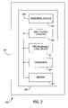
FIG. 3 is a simplified block diagram of an illustrative system employing a programmable logic device incorporating with the present invention.
DETAILED DESCRIPTION OF THE INVENTION
As described above, the present invention provides a programmable logic device in which cross-talk may be programmably eliminated or at least reduced by re-using unused DFE circuitry, associated with unused taps of CDR circuitry in the high-speed serial interface, for cross-talk cancellation or reduction.
Although every user logic design is different, once the design is fixed by the user, the sources and amounts of cross-talk become known at least to a degree. The present invention provides multiplexers at the inputs to the aforementioned DFE circuits to allow a user to programmably select either a CDR tap or a cross-talk source as the input to each DFE circuit. For any unused CDR tap in a channel that is subject to cross-talk, the user can select the corresponding DFE circuit to receive as its input a known source of cross-talk. The noise-rejection function of that DFE circuit is then used to generate a signal to cancel or at least reduce the cross-talk.
The DFE circuitry includes a programmable coefficient, with values preferably between 0 and 1. The value of the coefficient needed to cancel or reduce a particular cross-talk source will differ for each source. In accordance with the invention, the coefficients preferably are programmable by the user, or by circuitry provided for that purpose, to cancel or reduce the cross-talk. If done by the user, the coefficients essentially are varied manually by trial and error until the cross-talk is preferably eliminated or at least minimized as much as possible. Instead of using manual trial and error, circuitry can be constructed to similarly try all combinations of coefficient values until the best result is achieved. Alternatively, circuitry can be constructed with a correlation function that can identify the best coefficient value.
When the DFE circuitry is used on the CDR tap outputs, the signals being processed by the DFE circuitry inherently share a clock with the channel of which the CDR circuitry is a part. However, when unused DFE circuits are used to cancel or reduce cross-talk from a different channel or other source, it is unlikely that the cross-talk source will share a clock with the current channel. Therefore, a programmable time delay preferably also is provided. Again, the time delay can be adjusted by trial and error by the user or by circuitry. Because the user knows which cross-talk signals are being cancelled or reduced, the user can program the PLD so that most of the clock differential is compensated for prior to arrival of the cross-talk source signal at the DFE circuitry, and in such a case, the programmable time delay may be used only for fine tuning the clock differential adjustment. However, the programmable time delay also can be used to fully compensate for the clock differential.
The invention will now be described with reference to FIGS. 1 and 2.
FIG. 1 is a schematic representation of a receiver channel 10 including clock-data recovery circuitry. As shown, receiver 11 may have two inputs 111, 112 to accommodate a high-speed differential protocol (such as, e.g., LVDS), although the invention is applicable to single-ended protocols as well. The incoming signal, after initial processing in receiver 11, passes to CDR circuitry 12 through subtracter 13. The subtrahend signal for subtracter 13 is the received signal 113, while the minuend signal is a multibit output signal of n taps 120 of CDR circuitry 12 after processing of the tap outputs by respective ones of n DFE circuits 14. As seen, each of the n DFE circuits 14 includes an adjustable or programmable coefficient Cn. If d is the current data input to CDR circuitry 12, then each of n taps 120 represents one of the (d−1)st through (d−n)th data inputs. Each DFE circuit 14 thereby removes a portion, scaled by the respective coefficient Cn, of the interference contributed to the current data by the nth previous data.
In the known configuration of FIG. 1, the DFE circuitry is used to filter a wide distribution of noise or interference. In accordance with the present invention, as shown in FIG. 2, unused DFE circuits preferably can be used to attenuate or eliminate the deterministic interference contributed by a particular source or sources.
In each receiver channel 20 according to the invention, there preferably is interposed between a respective (d−n)th tap 120 and its associated DFE circuit 14 a selector, such as a multiplexer 21, that allows, as an alternative input into that respective DFE circuit 14, the output of a signal source 22 from outside channel 20. As shown in FIG. 2, no such selector is provided on the (d−1)st tap 120, because the computational resources necessary to generate a noise cancellation signal likely cannot operate quickly enough to cancel a noise component contributed only one bit period ago. However, in the event that sufficiently fast computational resources are available, it would not be outside the scope of the present invention to include a selector 21 on the (d−1)st tap 120. Optionally, and preferably, a variable time delay 23 is provided at the output of each respective DFE circuit 14 that has a selector 21 at its input, as discussed above and in more detail below.
Although channel 20 preferably is provided as a part of a general-purpose programmable logic device, for any particular user logic design, the user will know, or quickly determine, (a) which taps 120 are not being used, and (b) the characteristics of cross-talk sources 22. The user will therefore be able to select particular DFE circuits 14 to use for cross-talk reduction or cancellation, and to make the necessary adjustments to the coefficients Cn to effectively cancel, or reduce as much as possible, the cross-talk contributed by a particular source 22. The number of cross-talk sources and available unused DFE circuits 14 will differ for every channel 20. Preferably, the number of available DFE circuits 14 will not be less than the number of cross-talk sources, so that all cross-talk sources can be compensated for. It will be appreciated that the method described herein for using one DFE circuit 14 to reduce or eliminate cross-talk from one source 22 is duplicated for each source 22 that affects a particular channel, assuming that sufficient unused DFE circuits 14 are available. If sufficient unused DFE circuits 14 are not available, the user may have to decide which cross-talk source(s) 22 can be left uncompensated for with the least detrimental effect on channel 20.
In one embodiment, the user can provide, as part of the user logic design, the capability to adjust coefficients Cn manually. In a such an embodiment, the user can adjust the coefficients by trial and error, preferably aided by knowledge of the sources 22 to choose a starting setting close to the final setting, until the cross-talk is eliminated or at least minimized as much as possible. A similar result can be achieved by not providing an adjustment facility in the user logic design, but by simply reprogramming the programmable logic device with different coefficients until the desired result is achieved. This latter embodiment is somewhat less efficient in terms of the user's time, but may be more efficient because the adjustment facility will not have to be designed in creating the user logic design. Moreover, the “user” may not be the end user of the programmed programmable logic device, but rather the manufacturer of a product incorporating the programmable logic device who may not want to allow or require the end user to make the adjustments.
In another embodiment, circuitry can be provided as part of the user logic design to adjust the coefficients Cn automatically. One such embodiment can simply try all combinations until a best result is achieved. Alternatively, it may be possible to devise a circuit with a correlation function that can compute or otherwise determine the necessary coefficients based on the cross-talk inputs 22.
As described above, variable time delays 23 preferably are provided to compensate for the fact that a particular cross-talk source 22, which may be another I/O channel of the programmable logic device or may be a completely different type of circuit on the programmable logic device, is likely to have a clock that is completely different from that of channel 20. As also described above, each variable time delay 23 can be used for fine tuning the clock adjustment, with the primary (i.e., coarse) adjustment being made (not shown) on the input 22, based on the user's knowledge of the clocks of both channel 20 the various sources 22, or delay 23 can be used for the entire clock adjustment. Either way, the adjustments can be made manually as described above in connection with adjustment of coefficients Cn, or by circuitry created by the user to make the adjustments, again as described above in connection with adjustment of coefficients Cn.
Thus it is seen that circuitry in which cross-talk may be programmably eliminated, or at least reduced, by re-using unused portions of the high-speed serial interface has been provided.
A PLD 30 incorporating such circuitry according to the present invention may be used in many kinds of electronic devices. One possible use is in a data processing system 900 shown in FIG. 3. Data processing system 900 may include one or more of the following components: a processor 901; memory 902; I/O circuitry 903; and peripheral devices 904. These components are coupled together by a system bus 905 and are populated on a circuit board 906 which is contained in an end-user system 907.
System 900 can be used in a wide variety of applications, such as computer networking, data networking, instrumentation, video processing, digital signal processing, or any other application where the advantage of using programmable or reprogrammable logic is desirable. PLD 30 can be used to perform a variety of different logic functions. For example, PLD 30 can be configured as a processor or controller that works in cooperation with processor 901. PLD 30 may also be used as an arbiter for arbitrating access to a shared resources in system 900. In yet another example, PLD 30 can be configured as an interface between processor 901 and one of the other components in system 900. It should be noted that system 900 is only exemplary, and that the true scope and spirit of the invention should be indicated by the following claims.
Various technologies can be used to implement PLDs 30 as described above and incorporating this invention.
It will be understood that the foregoing is only illustrative of the principles of the invention, and that various modifications can be made by those skilled in the art without departing from the scope and spirit of the invention, and the present invention is limited only by the claims that follow.

Claims (15)

1. Clock-data recovery circuitry for a programmable logic device, said clock-data recovery circuitry being associated with an interface channel of said programmable logic device and being subject to cross-talk from at least one signal source on said programmable logic device separate from said interface channel, said clock-data recovery circuitry comprising:
a loop circuit having an input and a plurality of output taps, wherein (a) signals on both said input and said output taps are derived from said interface channel, and (b) the loop circuit at a given time uses fewer than said plurality of output taps;
a respective decision-feedback equalizer circuit accepting a respective output signal from each of at least one of said output taps, each said respective decision-feedback equalizer circuit having a programmable coefficient, and output of each said decision-feedback equalizer circuit being fed back to said input of said loop circuit;
at least one respective programmable selector between at least one respective one of said output taps and one said respective decision-feedback equalizer circuit, for programmably selecting between said output tap and said at least one signal source separate from said interface channel; wherein:
when said at least one respective one of said output taps is unused, said at least one signal source separate from said interface channel is programmably selected and applied to said respective decision-feedback equalizer circuit; and
said programmable coefficient is adjusted to minimize cross-talk from said one of said at least one signal source separate from said interface channel.
2. The clock-data recovery circuitry of claim 1 further comprising a programmable delay between said decision-feedback equalizer circuit and said input of said loop circuit.
3. The clock-data recovery circuitry of claim 1 wherein said selector comprises a multiplexer.
4. The clock-data recovery circuitry of claim 1 comprising:
a first set of decision-feedback equalizer circuits, said first set comprising at least one said decision-feedback equalizer circuit associated with a first said output tap;
a second set of decision feedback equalizer circuits comprising a plurality of said decision-feedback equalizer circuits, wherein each said decision-feedback equalizer circuit in said second set is associated with one of said output taps other than said first output tap; and
one said selector for each said decision-feedback equalizer circuit in said second set; whereby:
a plurality of said decision-feedback equalizer circuits are used for simultaneously cancelling cross-talk from a plurality of said at least one signal source separate from said interface channel.
5. A programmable logic device comprising the clock-data recovery circuitry of claim 1.
6. A digital processing system comprising:
processing circuitry;
a memory coupled to said processing circuitry; and
a programmable logic device as defined in claim 5 coupled to the processing circuitry and the memory.
7. A printed circuit board on which is mounted a programmable logic device as defined in claim 5.
8. The printed circuit board defined in claim 7 further comprising:
memory circuitry mounted on the printed circuit board and coupled to the programmable logic device.
9. The printed circuit board defined in claim 8 further comprising:
processing circuitry mounted on the printed circuit board and coupled to the memory circuitry.
10. An integrated circuit device comprising the clock-data recovery circuitry of claim 1.
11. A digital processing system comprising:
processing circuitry;
a memory coupled to said processing circuitry; and
an integrated circuit device as defined in claim 10 coupled to the processing circuitry and the memory.
12. A printed circuit board on which is mounted an integrated circuit device as defined in claim 11.
13. The printed circuit board defined in claim 12 further comprising:
memory circuitry mounted on the printed circuit board and coupled to the programmable logic device.
14. The printed circuit board defined in claim 13 further comprising:
processing circuitry mounted on the printed circuit board and coupled to the memory circuitry.
15. A method of cancelling cross-talk between an interface channel of a programmable logic device and at least one signal source on said programmable logic device separate from said interface channel, said programmable logic device comprising clock-data recovery circuitry, said method comprising:
receiving a signal derived from said interface channel at an input to a loop circuit, the loop circuit having a plurality of output taps, wherein the loop circuit at any given time uses fewer than said plurality of output taps;
receiving a respective output signal from each of at least one of said output taps at a respective decision-feedback equalizer circuit, each said respective decision-feedback equalizer circuit having a programmable coefficient, and output of each said decision-feedback equalizer circuit being fed back to the input of said loop circuit;
when said at least one respective one of said output taps is unused, programmably selecting and applying, with at least one programmable selector, one of said at least one signal source separate from said interface channel to said respective decision-feedback equalizer circuit; and
programmably adjusting a coefficient of said respective decision-feedback equalizer circuit to minimize cross-talk from said one of said at least one signal source separate from said interface channel.
US11/223,173 2005-09-08 2005-09-08 Programmable cross-talk cancellation in programmable logic device Expired - Fee Related US7526023B1 (en)

Priority Applications (1)

Application Number Priority Date Filing Date Title
US11/223,173 US7526023B1 (en) 2005-09-08 2005-09-08 Programmable cross-talk cancellation in programmable logic device

Applications Claiming Priority (1)

Application Number Priority Date Filing Date Title
US11/223,173 US7526023B1 (en) 2005-09-08 2005-09-08 Programmable cross-talk cancellation in programmable logic device

Publications (1)

Publication Number Publication Date
US7526023B1 true US7526023B1 (en) 2009-04-28

Family

ID=40568976

Family Applications (1)

Application Number Title Priority Date Filing Date
US11/223,173 Expired - Fee Related US7526023B1 (en) 2005-09-08 2005-09-08 Programmable cross-talk cancellation in programmable logic device

Country Status (1)

Country Link
US (1) US7526023B1 (en)

Cited By (7)

* Cited by examiner, † Cited by third party
Publication number Priority date Publication date Assignee Title
US20070025436A1 (en) * 2005-07-28 2007-02-01 Altera Corporation High-speed data reception circuitry and methods
US20070143811A1 (en) * 2005-12-21 2007-06-21 Broadcom Corporation Transceiver with Automatic Detection of Unshielded Twisted Pair or Shielded Twisted Pair Cabling
US20100067636A1 (en) * 2008-08-22 2010-03-18 Finisar Corporation Baseband Phase-Locked Loop
US20110085621A1 (en) * 2008-06-20 2011-04-14 Fujitsu Limited Receiver
CN107005506A (en) * 2014-12-16 2017-08-01 英特尔公司 Delayed elasticity decision feedback equalizer
US11240073B2 (en) * 2019-10-31 2022-02-01 Oracle International Corporation Adapative receiver with pre-cursor cancelation
US11290148B2 (en) * 2020-02-20 2022-03-29 Realtek Semiconductor Corporation Operation method and receiver device

Citations (4)

* Cited by examiner, † Cited by third party
Publication number Priority date Publication date Assignee Title
US20020154248A1 (en) * 2001-04-23 2002-10-24 Koninkli Jke Philips Electronics N.V. Generation of decision feedback equalizer data using trellis decoder traceback output in an ATSC HDTV receiver
US20030152173A1 (en) * 1999-07-30 2003-08-14 Strolle Christopher H. Diversity receiver with joint automatic gain control signal processing
US20050135471A1 (en) * 2003-12-19 2005-06-23 Davide Tonietto Integrated decision feedback equalizer and clock and data recovery
US20060146945A1 (en) * 2005-01-06 2006-07-06 Hong Kong Applied Science And Technology Research Institute Co., Ltd. Method and system for channel equalization and crosstalk estimation in a multicarrier data transmission system

Patent Citations (4)

* Cited by examiner, † Cited by third party
Publication number Priority date Publication date Assignee Title
US20030152173A1 (en) * 1999-07-30 2003-08-14 Strolle Christopher H. Diversity receiver with joint automatic gain control signal processing
US20020154248A1 (en) * 2001-04-23 2002-10-24 Koninkli Jke Philips Electronics N.V. Generation of decision feedback equalizer data using trellis decoder traceback output in an ATSC HDTV receiver
US20050135471A1 (en) * 2003-12-19 2005-06-23 Davide Tonietto Integrated decision feedback equalizer and clock and data recovery
US20060146945A1 (en) * 2005-01-06 2006-07-06 Hong Kong Applied Science And Technology Research Institute Co., Ltd. Method and system for channel equalization and crosstalk estimation in a multicarrier data transmission system

Cited By (15)

* Cited by examiner, † Cited by third party
Publication number Priority date Publication date Assignee Title
US20070025436A1 (en) * 2005-07-28 2007-02-01 Altera Corporation High-speed data reception circuitry and methods
US8743943B2 (en) * 2005-07-28 2014-06-03 Altera Corporation High-speed data reception circuitry and methods
US20070143811A1 (en) * 2005-12-21 2007-06-21 Broadcom Corporation Transceiver with Automatic Detection of Unshielded Twisted Pair or Shielded Twisted Pair Cabling
US20110085621A1 (en) * 2008-06-20 2011-04-14 Fujitsu Limited Receiver
US8619915B2 (en) * 2008-06-20 2013-12-31 Fujitsu Limited Receiver
US8358729B2 (en) * 2008-08-22 2013-01-22 Finisar Corporation Baseband phase-locked loop
US20100067636A1 (en) * 2008-08-22 2010-03-18 Finisar Corporation Baseband Phase-Locked Loop
CN107005506A (en) * 2014-12-16 2017-08-01 英特尔公司 Delayed elasticity decision feedback equalizer
EP3235203A4 (en) * 2014-12-16 2018-08-15 Intel Corporation Delay resilient decision feedback equalizer
US11240073B2 (en) * 2019-10-31 2022-02-01 Oracle International Corporation Adapative receiver with pre-cursor cancelation
US20220191071A1 (en) * 2019-10-31 2022-06-16 Oracle International Corporation Adaptive receiver with pre-cursor cancelation
US11558223B2 (en) * 2019-10-31 2023-01-17 Oracle International Corporation Adaptive receiver with pre-cursor cancelation
US20230155867A1 (en) * 2019-10-31 2023-05-18 Oracle International Corporation Adaptive receiver with pre-cursor cancelation
US11784855B2 (en) * 2019-10-31 2023-10-10 Oracle International Corporation Adaptive receiver with pre-cursor cancelation
US11290148B2 (en) * 2020-02-20 2022-03-29 Realtek Semiconductor Corporation Operation method and receiver device

Similar Documents

Publication Publication Date Title
US7526023B1 (en) Programmable cross-talk cancellation in programmable logic device
US9313054B1 (en) Circuits for and methods of filtering inter-symbol interference for SerDes applications
EP1010013B1 (en) Impedance control circuit
US6252419B1 (en) LVDS interface incorporating phase-locked loop circuitry for use in programmable logic device
US7821343B1 (en) Transmitter with multiple phase locked loops
KR102354962B1 (en) Decision Feedback Equalization with Precursor Inter-Symbol Interference Reduction
US7046174B1 (en) Byte alignment for serial data receiver
JP2018524855A (en) Channel-adaptive ADC-based receiver
US9030244B1 (en) Clock duty cycle calibration circuitry
US9385724B1 (en) Methods for operating configurable storage and processing blocks at double and single data rates
US9172566B1 (en) Methods and apparatus for multiple-stage CTLE adaptation
CN108292512B (en) Pipelined multiplexer loop architecture for decision feedback equalization circuits
JP5767337B2 (en) Adjustable finite impulse response transmitter
US8175143B1 (en) Adaptive equalization using data level detection
WO2018026460A1 (en) Dynamic clock-data phase alignment in a source synchronous interface circuit
US7352835B1 (en) Clock data recovery circuitry with dynamic support for changing data rates and a dynamically adjustable PPM detector
US7301996B1 (en) Skew cancellation for source synchronous clock and data signals
US20080205563A1 (en) Digital Filter
US20090086810A1 (en) Method and System for Static Data-Pattern Compensated Adaptive Equalizer Control
US9537681B1 (en) Multimode equalization circuitry
JP2022540562A (en) low latency receiver
WO2019091336A1 (en) Decision feedback equalizers and methods of decision feedback equalization
US9246715B1 (en) Pre-emphasis circuitry including a pre-emphasis voltage variation compensation engine
US20180218760A1 (en) Configurable storage blocks having simple first-in first-out enabling circuitry
US20020118741A1 (en) Waveform equalization apparatus

Legal Events

Date Code Title Description
AS Assignment

Owner name: ALTERA CORPORATION, CALIFORNIA

Free format text: ASSIGNMENT OF ASSIGNORS INTEREST;ASSIGNOR:SHUMARAYEV, SERGEY Y.;REEL/FRAME:016974/0872

Effective date: 20050901

STCF Information on status: patent grant

Free format text: PATENTED CASE

FPAY Fee payment

Year of fee payment: 4

FPAY Fee payment

Year of fee payment: 8

FEPP Fee payment procedure

Free format text: MAINTENANCE FEE REMINDER MAILED (ORIGINAL EVENT CODE: REM.); ENTITY STATUS OF PATENT OWNER: LARGE ENTITY

LAPS Lapse for failure to pay maintenance fees

Free format text: PATENT EXPIRED FOR FAILURE TO PAY MAINTENANCE FEES (ORIGINAL EVENT CODE: EXP.); ENTITY STATUS OF PATENT OWNER: LARGE ENTITY

STCH Information on status: patent discontinuation

Free format text: PATENT EXPIRED DUE TO NONPAYMENT OF MAINTENANCE FEES UNDER 37 CFR 1.362

FP Lapsed due to failure to pay maintenance fee

Effective date: 20210428