US7538440B2 - Method for improved high current component interconnections - Google Patents
Method for improved high current component interconnections Download PDFInfo
- Publication number
- US7538440B2 US7538440B2 US10/427,681 US42768103A US7538440B2 US 7538440 B2 US7538440 B2 US 7538440B2 US 42768103 A US42768103 A US 42768103A US 7538440 B2 US7538440 B2 US 7538440B2
- Authority
- US
- United States
- Prior art keywords
- solder
- printed circuit
- circuit board
- component
- solder paste
- Prior art date
- Legal status (The legal status is an assumption and is not a legal conclusion. Google has not performed a legal analysis and makes no representation as to the accuracy of the status listed.)
- Active, expires
Links
Images


Classifications
-
- H—ELECTRICITY
- H05—ELECTRIC TECHNIQUES NOT OTHERWISE PROVIDED FOR
- H05K—PRINTED CIRCUITS; CASINGS OR CONSTRUCTIONAL DETAILS OF ELECTRIC APPARATUS; MANUFACTURE OF ASSEMBLAGES OF ELECTRICAL COMPONENTS
- H05K3/00—Apparatus or processes for manufacturing printed circuits
- H05K3/30—Assembling printed circuits with electric components, e.g. with resistor
- H05K3/32—Assembling printed circuits with electric components, e.g. with resistor electrically connecting electric components or wires to printed circuits
- H05K3/34—Assembling printed circuits with electric components, e.g. with resistor electrically connecting electric components or wires to printed circuits by soldering
- H05K3/341—Surface mounted components
- H05K3/3431—Leadless components
- H05K3/3436—Leadless components having an array of bottom contacts, e.g. pad grid array or ball grid array components
-
- H—ELECTRICITY
- H05—ELECTRIC TECHNIQUES NOT OTHERWISE PROVIDED FOR
- H05K—PRINTED CIRCUITS; CASINGS OR CONSTRUCTIONAL DETAILS OF ELECTRIC APPARATUS; MANUFACTURE OF ASSEMBLAGES OF ELECTRICAL COMPONENTS
- H05K3/00—Apparatus or processes for manufacturing printed circuits
- H05K3/30—Assembling printed circuits with electric components, e.g. with resistor
- H05K3/32—Assembling printed circuits with electric components, e.g. with resistor electrically connecting electric components or wires to printed circuits
- H05K3/34—Assembling printed circuits with electric components, e.g. with resistor electrically connecting electric components or wires to printed circuits by soldering
- H05K3/3457—Solder materials or compositions; Methods of application thereof
- H05K3/3478—Applying solder preforms; Transferring prefabricated solder patterns
-
- H—ELECTRICITY
- H01—ELECTRIC ELEMENTS
- H01L—SEMICONDUCTOR DEVICES NOT COVERED BY CLASS H10
- H01L2924/00—Indexing scheme for arrangements or methods for connecting or disconnecting semiconductor or solid-state bodies as covered by H01L24/00
- H01L2924/0001—Technical content checked by a classifier
- H01L2924/0002—Not covered by any one of groups H01L24/00, H01L24/00 and H01L2224/00
-
- H—ELECTRICITY
- H05—ELECTRIC TECHNIQUES NOT OTHERWISE PROVIDED FOR
- H05K—PRINTED CIRCUITS; CASINGS OR CONSTRUCTIONAL DETAILS OF ELECTRIC APPARATUS; MANUFACTURE OF ASSEMBLAGES OF ELECTRICAL COMPONENTS
- H05K1/00—Printed circuits
- H05K1/02—Details
- H05K1/0213—Electrical arrangements not otherwise provided for
- H05K1/0263—High current adaptations, e.g. printed high current conductors or using auxiliary non-printed means; Fine and coarse circuit patterns on one circuit board
-
- H—ELECTRICITY
- H05—ELECTRIC TECHNIQUES NOT OTHERWISE PROVIDED FOR
- H05K—PRINTED CIRCUITS; CASINGS OR CONSTRUCTIONAL DETAILS OF ELECTRIC APPARATUS; MANUFACTURE OF ASSEMBLAGES OF ELECTRICAL COMPONENTS
- H05K2203/00—Indexing scheme relating to apparatus or processes for manufacturing printed circuits covered by H05K3/00
- H05K2203/04—Soldering or other types of metallurgic bonding
- H05K2203/041—Solder preforms in the shape of solder balls
-
- H—ELECTRICITY
- H05—ELECTRIC TECHNIQUES NOT OTHERWISE PROVIDED FOR
- H05K—PRINTED CIRCUITS; CASINGS OR CONSTRUCTIONAL DETAILS OF ELECTRIC APPARATUS; MANUFACTURE OF ASSEMBLAGES OF ELECTRICAL COMPONENTS
- H05K2203/00—Indexing scheme relating to apparatus or processes for manufacturing printed circuits covered by H05K3/00
- H05K2203/05—Patterning and lithography; Masks; Details of resist
- H05K2203/0548—Masks
- H05K2203/0557—Non-printed masks
-
- H—ELECTRICITY
- H05—ELECTRIC TECHNIQUES NOT OTHERWISE PROVIDED FOR
- H05K—PRINTED CIRCUITS; CASINGS OR CONSTRUCTIONAL DETAILS OF ELECTRIC APPARATUS; MANUFACTURE OF ASSEMBLAGES OF ELECTRICAL COMPONENTS
- H05K2203/00—Indexing scheme relating to apparatus or processes for manufacturing printed circuits covered by H05K3/00
- H05K2203/14—Related to the order of processing steps
- H05K2203/1476—Same or similar kind of process performed in phases, e.g. coarse patterning followed by fine patterning
-
- H—ELECTRICITY
- H05—ELECTRIC TECHNIQUES NOT OTHERWISE PROVIDED FOR
- H05K—PRINTED CIRCUITS; CASINGS OR CONSTRUCTIONAL DETAILS OF ELECTRIC APPARATUS; MANUFACTURE OF ASSEMBLAGES OF ELECTRICAL COMPONENTS
- H05K3/00—Apparatus or processes for manufacturing printed circuits
- H05K3/30—Assembling printed circuits with electric components, e.g. with resistor
- H05K3/32—Assembling printed circuits with electric components, e.g. with resistor electrically connecting electric components or wires to printed circuits
- H05K3/34—Assembling printed circuits with electric components, e.g. with resistor electrically connecting electric components or wires to printed circuits by soldering
- H05K3/3452—Solder masks
-
- H—ELECTRICITY
- H05—ELECTRIC TECHNIQUES NOT OTHERWISE PROVIDED FOR
- H05K—PRINTED CIRCUITS; CASINGS OR CONSTRUCTIONAL DETAILS OF ELECTRIC APPARATUS; MANUFACTURE OF ASSEMBLAGES OF ELECTRICAL COMPONENTS
- H05K3/00—Apparatus or processes for manufacturing printed circuits
- H05K3/30—Assembling printed circuits with electric components, e.g. with resistor
- H05K3/32—Assembling printed circuits with electric components, e.g. with resistor electrically connecting electric components or wires to printed circuits
- H05K3/34—Assembling printed circuits with electric components, e.g. with resistor electrically connecting electric components or wires to printed circuits by soldering
- H05K3/3457—Solder materials or compositions; Methods of application thereof
- H05K3/3485—Applying solder paste, slurry or powder
-
- Y—GENERAL TAGGING OF NEW TECHNOLOGICAL DEVELOPMENTS; GENERAL TAGGING OF CROSS-SECTIONAL TECHNOLOGIES SPANNING OVER SEVERAL SECTIONS OF THE IPC; TECHNICAL SUBJECTS COVERED BY FORMER USPC CROSS-REFERENCE ART COLLECTIONS [XRACs] AND DIGESTS
- Y02—TECHNOLOGIES OR APPLICATIONS FOR MITIGATION OR ADAPTATION AGAINST CLIMATE CHANGE
- Y02P—CLIMATE CHANGE MITIGATION TECHNOLOGIES IN THE PRODUCTION OR PROCESSING OF GOODS
- Y02P70/00—Climate change mitigation technologies in the production process for final industrial or consumer products
- Y02P70/50—Manufacturing or production processes characterised by the final manufactured product
Abstract
A printed circuit board having at least one conductive region covered in solder paste has preformed solder elements placed on the solder paste in the conductive region. A component package is placed onto the printed circuit board over the conductive region and the solder is reflowed, forming a wide solder interconnection between the component and the conductive region of the printed circuit board.
Description
1. Field of the Invention
The present invention relates generally to the field of electronic printed circuit boards, and more specifically to forming solder interconnections on the printed circuit board.
2. Discussion of Related Art
Demands on power delivery have increased as part of the effort to achieve higher performance in logic silicon products. Higher currents, better current transient response and bypass capacitance are frequently the key parameters sought in successful power delivery design. One potential power delivery bottleneck is in the printed circuit board -component interface. For example, a power MOSFET-board interface can introduce a substantial amount series resistance and thereby limit the effectiveness of the power delivery system. Currently, many standard off-the-shelf ball grid array (BGA) MOSFET components use similar interconnect structures for both the power and signal connection even though the electrical and thermal requirements for power and signaling can be different.
The relatively low volume solder ball of the BGA limits the size of the component-power plane interface. The smaller interconnects 122 formed using the prior art method limit current to the component. These smaller interconnects are highly resistive, and can limit the effectiveness of the power delivery system. In addition, the resulting high current density can result in excessive parasitic inductance. It is advantageous to remove this bottleneck by widening the power interface. A wider power interface has several advantages, including reduced resistance and increased heat transfer between the package and the printed circuit board. Though a wider power interface is desired, it is also advantageous to avoid altering the design of a commodity product like a MOSFET.
As illustrated in FIGS. 2A and 2B , a wider conductive interconnection may be formed on the printed circuit board by replacing an array of solder paste pads over a conductive region with a larger region of solder paste 109. This may not provide for an optimal solder interconnection, however. Solder paste 108 covers signal pads 104, forming an interconnection 122 between the signal pads and the component solder balls after solder reflow. Solder paste region 109 covers conductive plane 106, forming an interconnection 123 between the conductive plane and the component solder balls after solder reflow. As illustrated in FIG. 2B , the volume of solder provided by solder paste region 109 and solder balls 120 may not be sufficient to entirely fill the solder interconnection area 123 after solder reflow. Solder voids 124 and solder separation will result from insufficient solder volume. Furthermore, the resulting component standoff 126 will be less than the desired standoff when an inadequate amount of solder is used in forming interconnections.
In some cases, additional solder volume can be provided by the component, either by adding additional solder balls to the component, or by using larger solder balls on the component. However, this requires a change in product design by the component vendor to accommodate the additional solder on the component package.
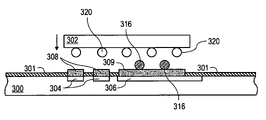
Embodiments of the present invention provide a method for widening the power delivery interface between the printed circuit board and the component through printed circuit board manufacturing processes alone, and without requiring a re-design of existing components. This is accomplished by placing pre-formed solder elements in selected areas of solder paste where additional solder volume is required.
In one embodiment of the present invention, the conductive planes 306 and the conductive signal pads 304 are copper.
Standard component packages are available in a wide variety of configurations. The array of solder balls on a component package in an embodiment of the present invention need not be identical to the arrays of solder balls shown in FIG. 8A or 8B. In one embodiment of the present invention, the component package is an unmodified, off -the-shelf package that is fully populated with solder balls. In another embodiment of the present invention, the component package is an unmodified, off-the-shelf package that is populated with solder balls around the periphery of the component package and having an open center cavity. In yet another embodiment of the present invention, the solder balls are equally sized and consistently spaced on the component package, and have a constant ball pitch.
Claims (4)
1. An apparatus comprising:
a printed circuit board including:
a conductive pad and a conductive plane having a larger surface area than the conductive pad;
a layer of solder paste applied to the conductive plane and conductive pad;
a plurality of printed circuit board solder elements in contact with the layer of solder paste applied to the conductive plane and the conductive pad; and
a component package containing a plurality of consistently spaced component solder elements;
wherein the component package is placeable onto the layer of solder paste applied to the conductive plane of the printed circuit board such that the plurality of printed circuit board solder elements are located interstitial to the plurality of consistently spaced component solder elements.
2. The apparatus of claim 1 wherein the component package has an open center cavity and a periphery populated with the plurality of consistently spaced component solder elements.
3. An apparatus comprising:
a printed circuit board including:
a conductive pad and a conductive plane having a larger surface area than the conductive pad;
a layer of solder paste applied to the conductive plane and conductive pad;
a plurality of printed circuit board solder elements in contact with the layer of solder paste applied to the conductive plane and the conductive pad; and
a component package containing a plurality of consistently spaced component solder elements;
wherein the component package is placeable onto the layer of solder paste applied to the conductive plane of the printed circuit board such that the plurality of printed circuit board solder elements are located between the plurality of consistently spaced component solder elements.
4. The apparatus of claim 3 wherein the component package has an open center cavity and a periphery populated with the plurality of consistently spaced component solder elements.
Priority Applications (3)
| Application Number | Priority Date | Filing Date | Title |
|---|---|---|---|
| US10/427,681 US7538440B2 (en) | 2003-04-30 | 2003-04-30 | Method for improved high current component interconnections |
| US11/148,535 US20050225953A1 (en) | 2003-04-30 | 2005-06-08 | Method for improved high current component interconnections |
| US11/657,197 US20070125833A1 (en) | 2003-04-30 | 2007-01-23 | Method for improved high current component interconnections |
Applications Claiming Priority (1)
| Application Number | Priority Date | Filing Date | Title |
|---|---|---|---|
| US10/427,681 US7538440B2 (en) | 2003-04-30 | 2003-04-30 | Method for improved high current component interconnections |
Related Child Applications (2)
| Application Number | Title | Priority Date | Filing Date |
|---|---|---|---|
| US11/148,535 Division US20050225953A1 (en) | 2003-04-30 | 2005-06-08 | Method for improved high current component interconnections |
| US11/657,197 Division US20070125833A1 (en) | 2003-04-30 | 2007-01-23 | Method for improved high current component interconnections |
Publications (2)
| Publication Number | Publication Date |
|---|---|
| US20040216917A1 US20040216917A1 (en) | 2004-11-04 |
| US7538440B2 true US7538440B2 (en) | 2009-05-26 |
Family
ID=33310225
Family Applications (3)
| Application Number | Title | Priority Date | Filing Date |
|---|---|---|---|
| US10/427,681 Active 2024-05-22 US7538440B2 (en) | 2003-04-30 | 2003-04-30 | Method for improved high current component interconnections |
| US11/148,535 Abandoned US20050225953A1 (en) | 2003-04-30 | 2005-06-08 | Method for improved high current component interconnections |
| US11/657,197 Abandoned US20070125833A1 (en) | 2003-04-30 | 2007-01-23 | Method for improved high current component interconnections |
Family Applications After (2)
| Application Number | Title | Priority Date | Filing Date |
|---|---|---|---|
| US11/148,535 Abandoned US20050225953A1 (en) | 2003-04-30 | 2005-06-08 | Method for improved high current component interconnections |
| US11/657,197 Abandoned US20070125833A1 (en) | 2003-04-30 | 2007-01-23 | Method for improved high current component interconnections |
Country Status (1)
| Country | Link |
|---|---|
| US (3) | US7538440B2 (en) |
Cited By (2)
| Publication number | Priority date | Publication date | Assignee | Title |
|---|---|---|---|---|
| US20080289863A1 (en) * | 2007-05-25 | 2008-11-27 | Princo Corp. | Surface finish structure of multi-layer substrate and manufacturing method thereof |
| US20130180772A1 (en) * | 2011-12-20 | 2013-07-18 | Ngk Spark Plug Co., Ltd. | Wiring board and method of manufacturing the same |
Families Citing this family (8)
| Publication number | Priority date | Publication date | Assignee | Title |
|---|---|---|---|---|
| US7538440B2 (en) | 2003-04-30 | 2009-05-26 | Intel Corporation | Method for improved high current component interconnections |
| US7955898B2 (en) | 2007-03-13 | 2011-06-07 | Micron Technology, Inc. | Packaged microelectronic devices and methods for manufacturing packaged microelectronic devices |
| US7780063B2 (en) * | 2008-05-15 | 2010-08-24 | International Business Machines Corporation | Techniques for arranging solder balls and forming bumps |
| CN101600292B (en) * | 2008-06-02 | 2012-06-20 | 鸿富锦精密工业(深圳)有限公司 | Circuit board |
| US8415567B1 (en) * | 2009-02-04 | 2013-04-09 | Rf Micro Devices, Inc. | Forming soldering surfaces without requiring a solder mask |
| US20120049359A1 (en) * | 2010-08-30 | 2012-03-01 | Wen-Jeng Fan | Ball grid array package |
| US10617000B2 (en) * | 2017-12-20 | 2020-04-07 | Intel Corporation | Printed circuit board (PCB) with three-dimensional interconnects to other printed circuit boards |
| CN113692126A (en) * | 2021-08-16 | 2021-11-23 | 北京梦之墨科技有限公司 | Circuit board, manufacturing method thereof and printing equipment |
Citations (26)
| Publication number | Priority date | Publication date | Assignee | Title |
|---|---|---|---|---|
| US4878611A (en) * | 1986-05-30 | 1989-11-07 | American Telephone And Telegraph Company, At&T Bell Laboratories | Process for controlling solder joint geometry when surface mounting a leadless integrated circuit package on a substrate |
| US5275330A (en) | 1993-04-12 | 1994-01-04 | International Business Machines Corp. | Solder ball connect pad-on-via assembly process |
| US5346118A (en) * | 1993-09-28 | 1994-09-13 | At&T Bell Laboratories | Surface mount solder assembly of leadless integrated circuit packages to substrates |
| JPH0738246A (en) | 1993-07-22 | 1995-02-07 | Fujitsu Ten Ltd | Soldering method and molding solder used therein |
| US5523920A (en) * | 1994-01-03 | 1996-06-04 | Motorola, Inc. | Printed circuit board comprising elevated bond pads |
| US5796590A (en) | 1996-11-05 | 1998-08-18 | Micron Electronics, Inc. | Assembly aid for mounting packaged integrated circuit devices to printed circuit boards |
| US5847936A (en) | 1997-06-20 | 1998-12-08 | Sun Microsystems, Inc. | Optimized routing scheme for an integrated circuit/printed circuit board |
| US5956606A (en) | 1997-10-31 | 1999-09-21 | Motorola, Inc. | Method for bumping and packaging semiconductor die |
| US6018197A (en) * | 1996-10-28 | 2000-01-25 | Ngk Spark Plug Co., Ltd. | Wired board with improved bonding pads |
| US6093964A (en) * | 1996-06-27 | 2000-07-25 | International Business Machines Corporation | Connection structure utilizing a metal bump and metal bump manufacturing method |
| US6165885A (en) * | 1995-08-02 | 2000-12-26 | International Business Machines Corporation | Method of making components with solder balls |
| US6319810B1 (en) | 1994-01-20 | 2001-11-20 | Fujitsu Limited | Method for forming solder bumps |
| US6358630B1 (en) * | 1997-06-04 | 2002-03-19 | Ibiden Co., Ltd. | Soldering member for printed wiring boards |
| US6380060B1 (en) | 2000-03-08 | 2002-04-30 | Tessera, Inc. | Off-center solder ball attach and methods therefor |
| US6410415B1 (en) * | 1999-03-23 | 2002-06-25 | Polymer Flip Chip Corporation | Flip chip mounting technique |
| US6514845B1 (en) | 1998-10-15 | 2003-02-04 | Texas Instruments Incorporated | Solder ball contact and method |
| US6548898B2 (en) * | 2000-12-28 | 2003-04-15 | Fujitsu Limited | External connection terminal and semiconductor device |
| US6697151B2 (en) * | 1999-04-07 | 2004-02-24 | Mv Research Limited | Material inspection |
| US6713871B2 (en) * | 2002-05-21 | 2004-03-30 | Intel Corporation | Surface mount solder method and apparatus for decoupling capacitance and process of making |
| US6740577B2 (en) * | 2002-05-21 | 2004-05-25 | St Assembly Test Services Pte Ltd | Method of forming a small pitch torch bump for mounting high-performance flip-flop devices |
| US6876072B1 (en) * | 2000-10-13 | 2005-04-05 | Bridge Semiconductor Corporation | Semiconductor chip assembly with chip in substrate cavity |
| US20050225953A1 (en) | 2003-04-30 | 2005-10-13 | Amir Dudi I | Method for improved high current component interconnections |
| US7109587B1 (en) * | 2004-05-25 | 2006-09-19 | National Semiconductor Corporation | Apparatus and method for enhanced thermal conductivity packages for high powered semiconductor devices |
| US7129577B2 (en) * | 2003-02-27 | 2006-10-31 | Power-One, Inc. | Power supply packaging system |
| US7138583B2 (en) * | 2002-05-08 | 2006-11-21 | Sandisk Corporation | Method and apparatus for maintaining a separation between contacts |
| US7301243B2 (en) * | 2004-08-30 | 2007-11-27 | Sharp Kabushiki Kaisha | High-reliable semiconductor device using hermetic sealing of electrodes |
Family Cites Families (9)
| Publication number | Priority date | Publication date | Assignee | Title |
|---|---|---|---|---|
| US4872261A (en) * | 1987-12-11 | 1989-10-10 | Digital Equipment Corporation | Method of and apparatus for surface mounting electronic components onto a printed wiring board |
| US5060844A (en) * | 1990-07-18 | 1991-10-29 | International Business Machines Corporation | Interconnection structure and test method |
| US5767580A (en) * | 1993-04-30 | 1998-06-16 | Lsi Logic Corporation | Systems having shaped, self-aligning micro-bump structures |
| US6253992B1 (en) * | 1998-03-18 | 2001-07-03 | Tessera, Inc. | Solder ball placement fixtures and methods |
| SG99331A1 (en) * | 2000-01-13 | 2003-10-27 | Hitachi Ltd | Method of producing electronic part with bumps and method of producing elctronic part |
| US6830463B2 (en) * | 2002-01-29 | 2004-12-14 | Fci Americas Technology, Inc. | Ball grid array connection device |
| US6793505B2 (en) * | 2002-03-26 | 2004-09-21 | Intel Corporation | Ganged land grid array socket contacts for improved power delivery |
| US6933449B2 (en) * | 2002-07-10 | 2005-08-23 | Intel Corporation | Selective area solder placement |
| US20050225942A1 (en) * | 2004-04-07 | 2005-10-13 | First International Computer Inc. | Plug-in cooling device |
-
2003
- 2003-04-30 US US10/427,681 patent/US7538440B2/en active Active
-
2005
- 2005-06-08 US US11/148,535 patent/US20050225953A1/en not_active Abandoned
-
2007
- 2007-01-23 US US11/657,197 patent/US20070125833A1/en not_active Abandoned
Patent Citations (27)
| Publication number | Priority date | Publication date | Assignee | Title |
|---|---|---|---|---|
| US4878611A (en) * | 1986-05-30 | 1989-11-07 | American Telephone And Telegraph Company, At&T Bell Laboratories | Process for controlling solder joint geometry when surface mounting a leadless integrated circuit package on a substrate |
| US5275330A (en) | 1993-04-12 | 1994-01-04 | International Business Machines Corp. | Solder ball connect pad-on-via assembly process |
| JPH0738246A (en) | 1993-07-22 | 1995-02-07 | Fujitsu Ten Ltd | Soldering method and molding solder used therein |
| US5346118A (en) * | 1993-09-28 | 1994-09-13 | At&T Bell Laboratories | Surface mount solder assembly of leadless integrated circuit packages to substrates |
| US5523920A (en) * | 1994-01-03 | 1996-06-04 | Motorola, Inc. | Printed circuit board comprising elevated bond pads |
| US6319810B1 (en) | 1994-01-20 | 2001-11-20 | Fujitsu Limited | Method for forming solder bumps |
| US6165885A (en) * | 1995-08-02 | 2000-12-26 | International Business Machines Corporation | Method of making components with solder balls |
| US6093964A (en) * | 1996-06-27 | 2000-07-25 | International Business Machines Corporation | Connection structure utilizing a metal bump and metal bump manufacturing method |
| US6018197A (en) * | 1996-10-28 | 2000-01-25 | Ngk Spark Plug Co., Ltd. | Wired board with improved bonding pads |
| US5796590A (en) | 1996-11-05 | 1998-08-18 | Micron Electronics, Inc. | Assembly aid for mounting packaged integrated circuit devices to printed circuit boards |
| US5930889A (en) * | 1996-11-05 | 1999-08-03 | Micron Electronics, Inc. | Method for mounting packaged integrated circuit devices to printed circuit boards |
| US6358630B1 (en) * | 1997-06-04 | 2002-03-19 | Ibiden Co., Ltd. | Soldering member for printed wiring boards |
| US5847936A (en) | 1997-06-20 | 1998-12-08 | Sun Microsystems, Inc. | Optimized routing scheme for an integrated circuit/printed circuit board |
| US5956606A (en) | 1997-10-31 | 1999-09-21 | Motorola, Inc. | Method for bumping and packaging semiconductor die |
| US6514845B1 (en) | 1998-10-15 | 2003-02-04 | Texas Instruments Incorporated | Solder ball contact and method |
| US6410415B1 (en) * | 1999-03-23 | 2002-06-25 | Polymer Flip Chip Corporation | Flip chip mounting technique |
| US6697151B2 (en) * | 1999-04-07 | 2004-02-24 | Mv Research Limited | Material inspection |
| US6380060B1 (en) | 2000-03-08 | 2002-04-30 | Tessera, Inc. | Off-center solder ball attach and methods therefor |
| US6876072B1 (en) * | 2000-10-13 | 2005-04-05 | Bridge Semiconductor Corporation | Semiconductor chip assembly with chip in substrate cavity |
| US6548898B2 (en) * | 2000-12-28 | 2003-04-15 | Fujitsu Limited | External connection terminal and semiconductor device |
| US7138583B2 (en) * | 2002-05-08 | 2006-11-21 | Sandisk Corporation | Method and apparatus for maintaining a separation between contacts |
| US6713871B2 (en) * | 2002-05-21 | 2004-03-30 | Intel Corporation | Surface mount solder method and apparatus for decoupling capacitance and process of making |
| US6740577B2 (en) * | 2002-05-21 | 2004-05-25 | St Assembly Test Services Pte Ltd | Method of forming a small pitch torch bump for mounting high-performance flip-flop devices |
| US7129577B2 (en) * | 2003-02-27 | 2006-10-31 | Power-One, Inc. | Power supply packaging system |
| US20050225953A1 (en) | 2003-04-30 | 2005-10-13 | Amir Dudi I | Method for improved high current component interconnections |
| US7109587B1 (en) * | 2004-05-25 | 2006-09-19 | National Semiconductor Corporation | Apparatus and method for enhanced thermal conductivity packages for high powered semiconductor devices |
| US7301243B2 (en) * | 2004-08-30 | 2007-11-27 | Sharp Kabushiki Kaisha | High-reliable semiconductor device using hermetic sealing of electrodes |
Non-Patent Citations (3)
| Title |
|---|
| Dudi I. Amir, "Improved High Current Component Interconnection", U.S. Appl. No. 11/148,535, filed on Jun. 8, 2005. Office Action mailed Jun. 27, 2006. Copy of the Office Action, claims as they stood in the application prior to the mailing of the Office Action. |
| U.S. Appl. No. 10/106,283, filed Mar. 26, 2002, "Ganged Land Grid Array Socket Contacts For Improved Power Delivery", 18 pages including Figures. |
| U.S. Appl. No. 10/192,346, filed Jul. 10, 2002, "Selective Area Solder Placement", 13 pages including Figures. |
Cited By (3)
| Publication number | Priority date | Publication date | Assignee | Title |
|---|---|---|---|---|
| US20080289863A1 (en) * | 2007-05-25 | 2008-11-27 | Princo Corp. | Surface finish structure of multi-layer substrate and manufacturing method thereof |
| US8294039B2 (en) * | 2007-05-25 | 2012-10-23 | Princo Middle East Fze | Surface finish structure of multi-layer substrate and manufacturing method thereof |
| US20130180772A1 (en) * | 2011-12-20 | 2013-07-18 | Ngk Spark Plug Co., Ltd. | Wiring board and method of manufacturing the same |
Also Published As
| Publication number | Publication date |
|---|---|
| US20050225953A1 (en) | 2005-10-13 |
| US20040216917A1 (en) | 2004-11-04 |
| US20070125833A1 (en) | 2007-06-07 |
Similar Documents
| Publication | Publication Date | Title |
|---|---|---|
| US20070125833A1 (en) | Method for improved high current component interconnections | |
| US6552421B2 (en) | Semiconductor device and a method of manufacturing the same | |
| US6515870B1 (en) | Package integrated faraday cage to reduce electromagnetic emissions from an integrated circuit | |
| JP3084230B2 (en) | Ball grid array package | |
| US6552436B2 (en) | Semiconductor device having a ball grid array and method therefor | |
| US6229209B1 (en) | Chip carrier | |
| US6553660B2 (en) | Electronic device and a method of manufacturing the same | |
| US5760469A (en) | Semiconductor device and semiconductor device mounting board | |
| JPH07202378A (en) | Packaged electron hardware unit | |
| US5469333A (en) | Electronic package assembly with protective encapsulant material on opposing sides not having conductive leads | |
| US7176561B2 (en) | Semiconductor device, method for manufacturing the same, circuit board, and electronic equipment | |
| JP2522889B2 (en) | Electronic package assembly and manufacturing method thereof | |
| US6034437A (en) | Semiconductor device having a matrix of bonding pads | |
| JP2009283828A (en) | Semiconductor device, and manufacturing method of semiconductor device | |
| US6320249B1 (en) | Multiple line grids incorporating therein circuit elements | |
| US20060226534A1 (en) | Structure and assembly method of integrated circuit package | |
| US6248951B1 (en) | Dielectric decal for a substrate of an integrated circuit package | |
| US9101058B2 (en) | IC package and assembly | |
| US6492715B1 (en) | Integrated semiconductor package | |
| US6963129B1 (en) | Multi-chip package having a contiguous heat spreader assembly | |
| US20060006533A1 (en) | Motherboard structure for preventing short circuit | |
| DE69433952T2 (en) | Package a BGA integrated circuit with high thermal conductivity | |
| US6291893B1 (en) | Power semiconductor device for “flip-chip” connections | |
| US20020030276A1 (en) | Dimple array interconnect technique for semiconductor device | |
| US7064279B2 (en) | Circuit board having an overlapping via |
Legal Events
| Date | Code | Title | Description |
|---|---|---|---|
| AS | Assignment |
Owner name: INTEL CORPORATION, CALIFORNIA Free format text: ASSIGNMENT OF ASSIGNORS INTEREST;ASSIGNORS:AMIR, DUDI I.;SEARLS, DAMION T.;REEL/FRAME:014031/0326;SIGNING DATES FROM 20030421 TO 20030423 |
|
| STCF | Information on status: patent grant |
Free format text: PATENTED CASE |
|
| FPAY | Fee payment |
Year of fee payment: 4 |
|
| FPAY | Fee payment |
Year of fee payment: 8 |
|
| MAFP | Maintenance fee payment |
Free format text: PAYMENT OF MAINTENANCE FEE, 12TH YEAR, LARGE ENTITY (ORIGINAL EVENT CODE: M1553); ENTITY STATUS OF PATENT OWNER: LARGE ENTITY Year of fee payment: 12 |