US7540920B2 - Silicon-containing layer deposition with silicon compounds - Google Patents
Silicon-containing layer deposition with silicon compounds Download PDFInfo
- Publication number
- US7540920B2 US7540920B2 US10/688,797 US68879703A US7540920B2 US 7540920 B2 US7540920 B2 US 7540920B2 US 68879703 A US68879703 A US 68879703A US 7540920 B2 US7540920 B2 US 7540920B2
- Authority
- US
- United States
- Prior art keywords
- silicon
- substrate
- source
- epitaxial layer
- crystalline surface
- Prior art date
- Legal status (The legal status is an assumption and is not a legal conclusion. Google has not performed a legal analysis and makes no representation as to the accuracy of the status listed.)
- Expired - Fee Related, expires
Links
- 0 C*(C)(C)[Si](C)(C)C Chemical compound C*(C)(C)[Si](C)(C)C 0.000 description 13
Classifications
-
- C—CHEMISTRY; METALLURGY
- C07—ORGANIC CHEMISTRY
- C07F—ACYCLIC, CARBOCYCLIC OR HETEROCYCLIC COMPOUNDS CONTAINING ELEMENTS OTHER THAN CARBON, HYDROGEN, HALOGEN, OXYGEN, NITROGEN, SULFUR, SELENIUM OR TELLURIUM
- C07F7/00—Compounds containing elements of Groups 4 or 14 of the Periodic System
- C07F7/02—Silicon compounds
- C07F7/08—Compounds having one or more C—Si linkages
- C07F7/0896—Compounds with a Si-H linkage
-
- C—CHEMISTRY; METALLURGY
- C01—INORGANIC CHEMISTRY
- C01B—NON-METALLIC ELEMENTS; COMPOUNDS THEREOF; METALLOIDS OR COMPOUNDS THEREOF NOT COVERED BY SUBCLASS C01C
- C01B33/00—Silicon; Compounds thereof
- C01B33/04—Hydrides of silicon
-
- C—CHEMISTRY; METALLURGY
- C01—INORGANIC CHEMISTRY
- C01B—NON-METALLIC ELEMENTS; COMPOUNDS THEREOF; METALLOIDS OR COMPOUNDS THEREOF NOT COVERED BY SUBCLASS C01C
- C01B33/00—Silicon; Compounds thereof
- C01B33/08—Compounds containing halogen
- C01B33/107—Halogenated silanes
-
- C—CHEMISTRY; METALLURGY
- C07—ORGANIC CHEMISTRY
- C07F—ACYCLIC, CARBOCYCLIC OR HETEROCYCLIC COMPOUNDS CONTAINING ELEMENTS OTHER THAN CARBON, HYDROGEN, HALOGEN, OXYGEN, NITROGEN, SULFUR, SELENIUM OR TELLURIUM
- C07F7/00—Compounds containing elements of Groups 4 or 14 of the Periodic System
- C07F7/02—Silicon compounds
- C07F7/08—Compounds having one or more C—Si linkages
- C07F7/12—Organo silicon halides
-
- C—CHEMISTRY; METALLURGY
- C23—COATING METALLIC MATERIAL; COATING MATERIAL WITH METALLIC MATERIAL; CHEMICAL SURFACE TREATMENT; DIFFUSION TREATMENT OF METALLIC MATERIAL; COATING BY VACUUM EVAPORATION, BY SPUTTERING, BY ION IMPLANTATION OR BY CHEMICAL VAPOUR DEPOSITION, IN GENERAL; INHIBITING CORROSION OF METALLIC MATERIAL OR INCRUSTATION IN GENERAL
- C23C—COATING METALLIC MATERIAL; COATING MATERIAL WITH METALLIC MATERIAL; SURFACE TREATMENT OF METALLIC MATERIAL BY DIFFUSION INTO THE SURFACE, BY CHEMICAL CONVERSION OR SUBSTITUTION; COATING BY VACUUM EVAPORATION, BY SPUTTERING, BY ION IMPLANTATION OR BY CHEMICAL VAPOUR DEPOSITION, IN GENERAL
- C23C16/00—Chemical coating by decomposition of gaseous compounds, without leaving reaction products of surface material in the coating, i.e. chemical vapour deposition [CVD] processes
- C23C16/22—Chemical coating by decomposition of gaseous compounds, without leaving reaction products of surface material in the coating, i.e. chemical vapour deposition [CVD] processes characterised by the deposition of inorganic material, other than metallic material
- C23C16/24—Deposition of silicon only
-
- C—CHEMISTRY; METALLURGY
- C23—COATING METALLIC MATERIAL; COATING MATERIAL WITH METALLIC MATERIAL; CHEMICAL SURFACE TREATMENT; DIFFUSION TREATMENT OF METALLIC MATERIAL; COATING BY VACUUM EVAPORATION, BY SPUTTERING, BY ION IMPLANTATION OR BY CHEMICAL VAPOUR DEPOSITION, IN GENERAL; INHIBITING CORROSION OF METALLIC MATERIAL OR INCRUSTATION IN GENERAL
- C23C—COATING METALLIC MATERIAL; COATING MATERIAL WITH METALLIC MATERIAL; SURFACE TREATMENT OF METALLIC MATERIAL BY DIFFUSION INTO THE SURFACE, BY CHEMICAL CONVERSION OR SUBSTITUTION; COATING BY VACUUM EVAPORATION, BY SPUTTERING, BY ION IMPLANTATION OR BY CHEMICAL VAPOUR DEPOSITION, IN GENERAL
- C23C16/00—Chemical coating by decomposition of gaseous compounds, without leaving reaction products of surface material in the coating, i.e. chemical vapour deposition [CVD] processes
- C23C16/22—Chemical coating by decomposition of gaseous compounds, without leaving reaction products of surface material in the coating, i.e. chemical vapour deposition [CVD] processes characterised by the deposition of inorganic material, other than metallic material
- C23C16/30—Deposition of compounds, mixtures or solid solutions, e.g. borides, carbides, nitrides
Landscapes
- Chemical & Material Sciences (AREA)
- Organic Chemistry (AREA)
- Inorganic Chemistry (AREA)
- Mechanical Engineering (AREA)
- Engineering & Computer Science (AREA)
- Materials Engineering (AREA)
- Chemical Kinetics & Catalysis (AREA)
- Metallurgy (AREA)
- General Chemical & Material Sciences (AREA)
- Chemical Vapour Deposition (AREA)
- Silicon Compounds (AREA)
- Carbon And Carbon Compounds (AREA)
- Recrystallisation Techniques (AREA)
Abstract
Description

wherein X1–X6 are independently hydrogen or halogen, R is carbon, silicon or germanium and X1–X6 comprise at least one hydrogen and at least one halogen.

wherein X1–X6 are independently hydrogen or halogen, R is carbon, silicon or germanium and X1–X6 comprise at least one hydrogen and at least one halogen and the proviso that R is not carbon when X4, X5 and X6 are fluorine.

wherein X1–X6 are independently hydrogen or halogen and R is germanium.

wherein X1–X8 are independently hydrogen or halogen, R is carbon, silicon or germanium and X1–X8 comprise at least one halogen.

wherein X1–X8 are independently hydrogen or halogen, R is carbon, silicon or germanium and X1–X8 comprise at least one halogen.

wherein X1–X8 are independently hydrogen or halogen and R is germanium.

wherein X1–X6 are independently hydrogen or halogen, R is carbon, silicon or germanium and X1–X6 comprise at least one hydrogen and at least one halogen.

wherein X1–X8 are independently hydrogen or halogen, R is carbon, silicon or germanium and X1–X8 comprise at least one halogen. In some embodiments, the silicon-containing film is selected from the group consisting of silicon, silicon germanium, silicon carbon and silicon germanium carbon.

where X1–X10 are independently hydrogen or halogen, such as fluorine, chlorine, bromine or iodine and R is carbon, silicon or germanium.
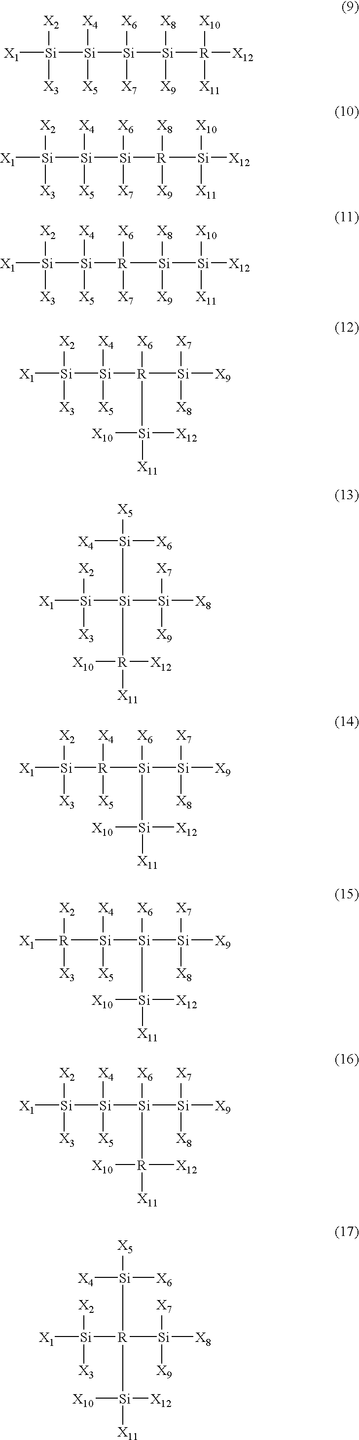


where X1–X12 are independently hydrogen or halogen, such as fluorine, chlorine, bromine or iodine and R is carbon, silicon or germanium. The structures of compounds 1–32 are representative and do not imply a particular isomer. Herein, any elemental name or chemical symbol anticipates the use of the respective elemental isotopes, such as the use of hydrogen (1H or H) also includes the use of deuterium (2H or D) and tritium (3H or T).
Claims (72)


Priority Applications (10)
| Application Number | Priority Date | Filing Date | Title |
|---|---|---|---|
| US10/688,797 US7540920B2 (en) | 2002-10-18 | 2003-10-17 | Silicon-containing layer deposition with silicon compounds |
| KR1020057006706A KR101144366B1 (en) | 2002-10-18 | 2003-10-20 | Silicon-containing layer deposition with silicon compounds |
| EP03809181.5A EP1563529B1 (en) | 2002-10-18 | 2003-10-20 | Silicon-containing layer deposition with silicon compounds |
| AU2003301382A AU2003301382A1 (en) | 2002-10-18 | 2003-10-20 | Silicon-containing layer deposition with silicon compounds |
| PCT/US2003/033263 WO2004036631A2 (en) | 2002-10-18 | 2003-10-20 | Silicon-containing layer deposition with silicon compounds |
| JP2004545570A JP2006515955A (en) | 2002-10-18 | 2003-10-20 | Deposition of silicon-containing layers with silicon compounds |
| US11/549,033 US7645339B2 (en) | 2002-10-18 | 2006-10-12 | Silicon-containing layer deposition with silicon compounds |
| US11/969,139 US7758697B2 (en) | 2002-10-18 | 2008-01-03 | Silicon-containing layer deposition with silicon compounds |
| JP2010133104A JP5593129B2 (en) | 2002-10-18 | 2010-06-10 | Deposition of silicon-containing layers with silicon compounds |
| JP2013203938A JP2014027294A (en) | 2002-10-18 | 2013-09-30 | Silicon-containing layer deposition with silicon compounds |
Applications Claiming Priority (4)
| Application Number | Priority Date | Filing Date | Title |
|---|---|---|---|
| US41937602P | 2002-10-18 | 2002-10-18 | |
| US41942602P | 2002-10-18 | 2002-10-18 | |
| US41950402P | 2002-10-18 | 2002-10-18 | |
| US10/688,797 US7540920B2 (en) | 2002-10-18 | 2003-10-17 | Silicon-containing layer deposition with silicon compounds |
Related Child Applications (2)
| Application Number | Title | Priority Date | Filing Date |
|---|---|---|---|
| US11/549,033 Continuation US7645339B2 (en) | 2002-10-18 | 2006-10-12 | Silicon-containing layer deposition with silicon compounds |
| US11/969,139 Continuation US7758697B2 (en) | 2002-10-18 | 2008-01-03 | Silicon-containing layer deposition with silicon compounds |
Publications (2)
| Publication Number | Publication Date |
|---|---|
| US20040224089A1 US20040224089A1 (en) | 2004-11-11 |
| US7540920B2 true US7540920B2 (en) | 2009-06-02 |
Family
ID=32111050
Family Applications (3)
| Application Number | Title | Priority Date | Filing Date |
|---|---|---|---|
| US10/688,797 Expired - Fee Related US7540920B2 (en) | 2002-10-18 | 2003-10-17 | Silicon-containing layer deposition with silicon compounds |
| US11/549,033 Expired - Fee Related US7645339B2 (en) | 2002-10-18 | 2006-10-12 | Silicon-containing layer deposition with silicon compounds |
| US11/969,139 Expired - Fee Related US7758697B2 (en) | 2002-10-18 | 2008-01-03 | Silicon-containing layer deposition with silicon compounds |
Family Applications After (2)
| Application Number | Title | Priority Date | Filing Date |
|---|---|---|---|
| US11/549,033 Expired - Fee Related US7645339B2 (en) | 2002-10-18 | 2006-10-12 | Silicon-containing layer deposition with silicon compounds |
| US11/969,139 Expired - Fee Related US7758697B2 (en) | 2002-10-18 | 2008-01-03 | Silicon-containing layer deposition with silicon compounds |
Country Status (6)
| Country | Link |
|---|---|
| US (3) | US7540920B2 (en) |
| EP (1) | EP1563529B1 (en) |
| JP (3) | JP2006515955A (en) |
| KR (1) | KR101144366B1 (en) |
| AU (1) | AU2003301382A1 (en) |
| WO (1) | WO2004036631A2 (en) |
Cited By (18)
| Publication number | Priority date | Publication date | Assignee | Title |
|---|---|---|---|---|
| US8012859B1 (en) * | 2010-03-31 | 2011-09-06 | Tokyo Electron Limited | Atomic layer deposition of silicon and silicon-containing films |
| US8916425B2 (en) | 2010-07-26 | 2014-12-23 | Semiconductor Energy Laboratory Co., Ltd. | Method for forming microcrystalline semiconductor film and method for manufacturing semiconductor device |
| US9018108B2 (en) | 2013-01-25 | 2015-04-28 | Applied Materials, Inc. | Low shrinkage dielectric films |
| US20150303060A1 (en) * | 2014-04-16 | 2015-10-22 | Samsung Electronics Co., Ltd. | Silicon precursor, method of forming a layer using the same, and method of fabricating semiconductor device using the same |
| US9337018B2 (en) | 2012-06-01 | 2016-05-10 | Air Products And Chemicals, Inc. | Methods for depositing films with organoaminodisilane precursors |
| US9472392B2 (en) | 2015-01-30 | 2016-10-18 | Applied Materials, Inc. | Step coverage dielectric |
| US9633838B2 (en) | 2015-12-28 | 2017-04-25 | L'Air Liquide, Société Anonyme pour l'Etude et l'Exploitation des Procédés Georges Claude | Vapor deposition of silicon-containing films using penta-substituted disilanes |
| WO2018057677A1 (en) * | 2016-09-26 | 2018-03-29 | Dow Corning Corporation | Trichlorodisilane |
| EP3410466A1 (en) | 2017-06-01 | 2018-12-05 | Evonik Degussa GmbH | Chlorosilylarylgermane derivatives, process for their production and use thereof |
| EP3409678A1 (en) | 2017-06-01 | 2018-12-05 | Evonik Degussa GmbH | New halogen germanides and method for their preparation |
| EP3409645A1 (en) | 2017-06-01 | 2018-12-05 | Evonik Degussa GmbH | Triphenylgermylsilane and trichlorsilyl-trichlorgermane for the production of germanium-silicon layers as well as processes for their preparation from trichlorsilyl-triphenylgermane |
| WO2019005571A1 (en) * | 2017-06-29 | 2019-01-03 | Dow Silicones Corporation | Synthesis of 1,1,1-trichlorodisilane |
| US10395917B2 (en) | 2013-03-14 | 2019-08-27 | Asm Ip Holding B.V. | Si precursors for deposition of SiN at low temperatures |
| US10424477B2 (en) | 2013-03-14 | 2019-09-24 | Asm Ip Holding B.V. | Si precursors for deposition of SiN at low temperatures |
| US11011635B2 (en) | 2016-12-12 | 2021-05-18 | Applied Materials, Inc. | Method of forming conformal epitaxial semiconductor cladding material over a fin field effect transistor (FINFET) device |
| US11145504B2 (en) | 2019-01-14 | 2021-10-12 | Applied Materials, Inc. | Method of forming film stacks with reduced defects |
| US11367613B2 (en) | 2014-09-17 | 2022-06-21 | Asm Ip Holding B.V. | Deposition of SiN |
| US11784043B2 (en) | 2015-08-24 | 2023-10-10 | ASM IP Holding, B.V. | Formation of SiN thin films |
Families Citing this family (75)
| Publication number | Priority date | Publication date | Assignee | Title |
|---|---|---|---|---|
| AU2002306436A1 (en) | 2001-02-12 | 2002-10-15 | Asm America, Inc. | Improved process for deposition of semiconductor films |
| US7439191B2 (en) * | 2002-04-05 | 2008-10-21 | Applied Materials, Inc. | Deposition of silicon layers for active matrix liquid crystal display (AMLCD) applications |
| US7186630B2 (en) | 2002-08-14 | 2007-03-06 | Asm America, Inc. | Deposition of amorphous silicon-containing films |
| US7468311B2 (en) * | 2003-09-30 | 2008-12-23 | Tokyo Electron Limited | Deposition of silicon-containing films from hexachlorodisilane |
| US7166528B2 (en) | 2003-10-10 | 2007-01-23 | Applied Materials, Inc. | Methods of selective deposition of heavily doped epitaxial SiGe |
| US6987055B2 (en) * | 2004-01-09 | 2006-01-17 | Micron Technology, Inc. | Methods for deposition of semiconductor material |
| KR20070006852A (en) * | 2004-04-23 | 2007-01-11 | 에이에스엠 아메리카, 인코포레이티드 | In situ doped epitaxial films |
| US20050252449A1 (en) | 2004-05-12 | 2005-11-17 | Nguyen Son T | Control of gas flow and delivery to suppress the formation of particles in an MOCVD/ALD system |
| US7981392B2 (en) | 2004-09-14 | 2011-07-19 | The Arizona Board Of Regents, A Body Corporate Of The State Of Arizona Acting For And On Behalf Of Arizona State University | Hydride compounds with silicon and germanium core atoms and method of synthesizing same |
| JP2008513979A (en) * | 2004-09-14 | 2008-05-01 | アリゾナ ボード オブ リージェンツ ア ボディー コーポレート アクティング オン ビハーフ オブ アリゾナ ステイト ユニバーシティ | Si-Ge semiconductor material and device growth method on a substrate |
| US20060071213A1 (en) * | 2004-10-04 | 2006-04-06 | Ce Ma | Low temperature selective epitaxial growth of silicon germanium layers |
| US7015153B1 (en) * | 2004-10-20 | 2006-03-21 | Freescale Semiconductor, Inc. | Method for forming a layer using a purging gas in a semiconductor process |
| KR100585175B1 (en) * | 2005-01-31 | 2006-05-30 | 삼성전자주식회사 | Fabrication method of gesbte thin film by chemical vapor deposition process |
| US7816236B2 (en) | 2005-02-04 | 2010-10-19 | Asm America Inc. | Selective deposition of silicon-containing films |
| KR100642646B1 (en) * | 2005-07-08 | 2006-11-10 | 삼성전자주식회사 | Methods of selectively forming an epitaxial semiconductor layer using a ultra high vacuum chemical vapor deposition technique and batch-type ultra high vacuum chemical vapor deposition apparatus used therein |
| US20070048956A1 (en) * | 2005-08-30 | 2007-03-01 | Tokyo Electron Limited | Interrupted deposition process for selective deposition of Si-containing films |
| US20090087967A1 (en) * | 2005-11-14 | 2009-04-02 | Todd Michael A | Precursors and processes for low temperature selective epitaxial growth |
| JP5265377B2 (en) * | 2005-11-23 | 2013-08-14 | アリゾナ ボード オブ リージェンツ ア ボディー コーポレート アクティング オン ビハーフ オブ アリゾナ ステイト ユニバーシティ | Novel silicon germanium hydride, its production and use |
| JP5265376B2 (en) | 2005-11-23 | 2013-08-14 | アリゾナ ボード オブ リージェンツ ア ボディー コーポレート アクティング オン ビハーフ オブ アリゾナ ステイト ユニバーシティ | Novel silicon germanium hydride, its production and use |
| JP2009521801A (en) * | 2005-12-22 | 2009-06-04 | エーエスエム アメリカ インコーポレイテッド | Epitaxial deposition of doped semiconductor materials. |
| KR100695168B1 (en) * | 2006-01-10 | 2007-03-14 | 삼성전자주식회사 | Method of forming phase change material thin film, and method of manufacturing phase change memory device using the same |
| US7798096B2 (en) | 2006-05-05 | 2010-09-21 | Applied Materials, Inc. | Plasma, UV and ion/neutral assisted ALD or CVD in a batch tool |
| US20080026149A1 (en) * | 2006-05-31 | 2008-01-31 | Asm America, Inc. | Methods and systems for selectively depositing si-containing films using chloropolysilanes |
| US8278176B2 (en) | 2006-06-07 | 2012-10-02 | Asm America, Inc. | Selective epitaxial formation of semiconductor films |
| DE102006034061A1 (en) * | 2006-07-20 | 2008-01-24 | REV Renewable Energy Ventures, Inc., Aloha | Polysilane processing and use |
| DE102006043929B4 (en) * | 2006-09-14 | 2016-10-06 | Spawnt Private S.À.R.L. | Process for the preparation of solid polysilane mixtures |
| WO2008051328A1 (en) * | 2006-10-24 | 2008-05-02 | Dow Corning Corporation | Composition comprising neopentasilane and method of preparing same |
| US7837790B2 (en) * | 2006-12-01 | 2010-11-23 | Applied Materials, Inc. | Formation and treatment of epitaxial layer containing silicon and carbon |
| US7741200B2 (en) * | 2006-12-01 | 2010-06-22 | Applied Materials, Inc. | Formation and treatment of epitaxial layer containing silicon and carbon |
| US20080132039A1 (en) * | 2006-12-01 | 2008-06-05 | Yonah Cho | Formation and treatment of epitaxial layer containing silicon and carbon |
| US7897495B2 (en) * | 2006-12-12 | 2011-03-01 | Applied Materials, Inc. | Formation of epitaxial layer containing silicon and carbon |
| US7960236B2 (en) * | 2006-12-12 | 2011-06-14 | Applied Materials, Inc. | Phosphorus containing Si epitaxial layers in N-type source/drain junctions |
| US20080138955A1 (en) * | 2006-12-12 | 2008-06-12 | Zhiyuan Ye | Formation of epitaxial layer containing silicon |
| US8394196B2 (en) * | 2006-12-12 | 2013-03-12 | Applied Materials, Inc. | Formation of in-situ phosphorus doped epitaxial layer containing silicon and carbon |
| US9064960B2 (en) * | 2007-01-31 | 2015-06-23 | Applied Materials, Inc. | Selective epitaxy process control |
| DE102007007874A1 (en) * | 2007-02-14 | 2008-08-21 | Evonik Degussa Gmbh | Process for the preparation of higher silanes |
| CN101678665B (en) * | 2007-04-02 | 2013-07-10 | 代表亚利桑那州立大学行事的亚利桑那董事会 | Novel methods for making and using halosilylgermanes |
| US7915104B1 (en) | 2007-06-04 | 2011-03-29 | The Arizona Board Of Regents, A Body Corporate Of The State Of Arizona Acting For And On Behalf Of Arizona State University | Methods and compositions for preparing tensile strained Ge on Ge1-ySny buffered semiconductor substrates |
| TWI347000B (en) * | 2007-06-11 | 2011-08-11 | Xintec Inc | Integrated circuit package and operation, fabrication method thereof |
| KR101028416B1 (en) * | 2007-08-20 | 2011-04-13 | 재단법인서울대학교산학협력재단 | Method for production of thin film and apparatus for manufacturing the same |
| US7759199B2 (en) | 2007-09-19 | 2010-07-20 | Asm America, Inc. | Stressor for engineered strain on channel |
| US7776698B2 (en) | 2007-10-05 | 2010-08-17 | Applied Materials, Inc. | Selective formation of silicon carbon epitaxial layer |
| JP4933399B2 (en) * | 2007-10-25 | 2012-05-16 | 株式会社ニューフレアテクノロジー | Semiconductor manufacturing method and semiconductor manufacturing apparatus |
| US7939447B2 (en) | 2007-10-26 | 2011-05-10 | Asm America, Inc. | Inhibitors for selective deposition of silicon containing films |
| US7655543B2 (en) * | 2007-12-21 | 2010-02-02 | Asm America, Inc. | Separate injection of reactive species in selective formation of films |
| US7659158B2 (en) | 2008-03-31 | 2010-02-09 | Applied Materials, Inc. | Atomic layer deposition processes for non-volatile memory devices |
| US8486191B2 (en) | 2009-04-07 | 2013-07-16 | Asm America, Inc. | Substrate reactor with adjustable injectors for mixing gases within reaction chamber |
| US8367528B2 (en) | 2009-11-17 | 2013-02-05 | Asm America, Inc. | Cyclical epitaxial deposition and etch |
| DE102009056436B4 (en) * | 2009-12-02 | 2013-06-27 | Spawnt Private S.À.R.L. | Chloride-containing silicon |
| DE102010002405A1 (en) | 2010-02-26 | 2011-09-01 | Evonik Degussa Gmbh | A process for the oligomerization of hydridosilanes, the process of preparing oligomerizates and their use |
| JP6296793B2 (en) | 2010-04-06 | 2018-03-20 | シン フィルム エレクトロニクス エーエスエー | Epitaxial structure, method for forming the same, and device including the same |
| JP5847566B2 (en) * | 2011-01-14 | 2016-01-27 | 株式会社日立国際電気 | Semiconductor device manufacturing method, substrate processing method, substrate processing apparatus, and program |
| US8809170B2 (en) | 2011-05-19 | 2014-08-19 | Asm America Inc. | High throughput cyclical epitaxial deposition and etch process |
| WO2013078219A1 (en) * | 2011-11-23 | 2013-05-30 | University Of South Carolina | Method of growing high quality, thick sic epitaxial films by eliminating silicon gas phase nucleation and suppressing parasitic deposition |
| US20130193492A1 (en) * | 2012-01-30 | 2013-08-01 | International Business Machines Corporation | Silicon carbon film structure and method |
| JP5959907B2 (en) * | 2012-04-12 | 2016-08-02 | 株式会社日立国際電気 | Semiconductor device manufacturing method, substrate processing method, substrate processing apparatus, and program |
| JP5926794B2 (en) * | 2012-04-23 | 2016-05-25 | 東京エレクトロン株式会社 | Film forming method, film forming apparatus, and film forming system |
| US9147574B2 (en) | 2013-03-14 | 2015-09-29 | Tokyo Electron Limited | Topography minimization of neutral layer overcoats in directed self-assembly applications |
| JP2015053382A (en) * | 2013-09-06 | 2015-03-19 | 株式会社日本触媒 | Silicon-containing epitaxial film, manufacturing method thereof, and semiconductor device |
| EP3298177A1 (en) | 2015-05-22 | 2018-03-28 | Dow Corning Corporation | Pentachlorosilane |
| US10056264B2 (en) * | 2015-06-05 | 2018-08-21 | Lam Research Corporation | Atomic layer etching of GaN and other III-V materials |
| JP6086942B2 (en) * | 2015-06-10 | 2017-03-01 | 株式会社日立国際電気 | Semiconductor device manufacturing method, substrate processing apparatus, and program |
| KR102352232B1 (en) | 2015-06-15 | 2022-01-17 | 삼성전자주식회사 | Method of fabricating semiconductor device having contact structures |
| TWI663281B (en) * | 2015-06-16 | 2019-06-21 | 美商慧盛材料美國責任有限公司 | Preparation and composition of halidosilane compounds, and container containing same |
| KR102441431B1 (en) | 2016-06-06 | 2022-09-06 | 어플라이드 머티어리얼스, 인코포레이티드 | Processing methods comprising positioning a substrate with a surface in a processing chamber |
| TWI757478B (en) * | 2017-05-02 | 2022-03-11 | 美商應用材料股份有限公司 | Methods of forming tungsten pillars |
| US10580645B2 (en) | 2018-04-30 | 2020-03-03 | Asm Ip Holding B.V. | Plasma enhanced atomic layer deposition (PEALD) of SiN using silicon-hydrohalide precursors |
| KR102346832B1 (en) * | 2018-05-23 | 2022-01-03 | 삼성에스디아이 주식회사 | Etching composition for silicon nitride layer and etching process using the same |
| EP3587348B1 (en) * | 2018-06-29 | 2021-08-11 | Evonik Operations GmbH | Partially hydrogenated chlorosilanes and methods for preparing same by selective hydrogenation |
| US20200017970A1 (en) * | 2018-07-12 | 2020-01-16 | Lotus Applied Technology, Llc | Water-insensitive methods of forming metal oxide films and products related thereto |
| EP3653577B1 (en) | 2018-11-14 | 2021-10-06 | Evonik Operations GmbH | Tris(trichlorsilyl)dichlorogallylgerman, method for producing same and its use |
| EP3653578B1 (en) | 2018-11-14 | 2021-04-21 | Evonik Operations GmbH | Tetrakis(trichlorsilyl) german, method for producing same |
| DE102020114994A1 (en) | 2020-06-05 | 2021-12-09 | Johann Wolfgang Goethe-Universität Frankfurt am Main Stiftung des öffentlichen Rechts | Silylated oligogerman, process for the production of the same and the use of the same for the production of a solid containing Si and Ge |
| CN116194615A (en) | 2020-06-05 | 2023-05-30 | 约翰-沃尔福冈-歌德大学 | Silylated oligogermanes and polycyclic silicon-germanium compounds, methods for the production thereof, and use thereof for producing solids containing Si and Ge |
| EP4251631A1 (en) | 2020-11-27 | 2023-10-04 | Johann Wolfgang Goethe-Universität | Polycyclic silicon-germanium compounds, process of preparing same and their use for producing a si- and ge-containing solid |
Citations (79)
| Publication number | Priority date | Publication date | Assignee | Title |
|---|---|---|---|---|
| US4690830A (en) | 1986-02-18 | 1987-09-01 | Solarex Corporation | Activation by dehydrogenation or dehalogenation of deposition feedstock and dopant materials useful in the fabrication of hydrogenated amorphous silicon alloys for photovoltaic devices and other semiconductor devices |
| US4830890A (en) | 1985-12-24 | 1989-05-16 | Canon Kabushiki Kaisha | Method for forming a deposited film from a gaseous silane compound heated on a substrate and introducing an active species therewith |
| US4834831A (en) | 1986-09-08 | 1989-05-30 | Research Development Corporation Of Japan | Method for growing single crystal thin films of element semiconductor |
| US4990374A (en) * | 1989-11-28 | 1991-02-05 | Cvd Incorporated | Selective area chemical vapor deposition |
| US5112439A (en) | 1988-11-30 | 1992-05-12 | Mcnc | Method for selectively depositing material on substrates |
| US5273930A (en) | 1992-09-03 | 1993-12-28 | Motorola, Inc. | Method of forming a non-selective silicon-germanium epitaxial film |
| US5294286A (en) | 1984-07-26 | 1994-03-15 | Research Development Corporation Of Japan | Process for forming a thin film of silicon |
| US5372860A (en) | 1993-07-06 | 1994-12-13 | Corning Incorporated | Silicon device production |
| US5374570A (en) | 1989-03-17 | 1994-12-20 | Fujitsu Limited | Method of manufacturing active matrix display device using insulation layer formed by the ale method |
| US5469806A (en) | 1992-08-21 | 1995-11-28 | Nec Corporation | Method for epitaxial growth of semiconductor crystal by using halogenide |
| US5480818A (en) | 1992-02-10 | 1996-01-02 | Fujitsu Limited | Method for forming a film and method for manufacturing a thin film transistor |
| US5503875A (en) | 1993-03-18 | 1996-04-02 | Tokyo Electron Limited | Film forming method wherein a partial pressure of a reaction byproduct in a processing container is reduced temporarily |
| US5521126A (en) | 1993-06-25 | 1996-05-28 | Nec Corporation | Method of fabricating semiconductor devices |
| US5527733A (en) | 1989-07-27 | 1996-06-18 | Seiko Instruments Inc. | Impurity doping method with adsorbed diffusion source |
| US5604151A (en) | 1992-11-23 | 1997-02-18 | Cvd, Incorporated | Chemical vapor deposition-produced silicon carbide having improved properties |
| US5674304A (en) | 1993-10-12 | 1997-10-07 | Semiconductor Energy Laboratory Co., Ltd. | Method of heat-treating a glass substrate |
| US5693139A (en) | 1984-07-26 | 1997-12-02 | Research Development Corporation Of Japan | Growth of doped semiconductor monolayers |
| US5796116A (en) | 1994-07-27 | 1998-08-18 | Sharp Kabushiki Kaisha | Thin-film semiconductor device including a semiconductor film with high field-effect mobility |
| US5807792A (en) | 1996-12-18 | 1998-09-15 | Siemens Aktiengesellschaft | Uniform distribution of reactants in a device layer |
| US5906680A (en) | 1986-09-12 | 1999-05-25 | International Business Machines Corporation | Method and apparatus for low temperature, low pressure chemical vapor deposition of epitaxial silicon layers |
| US5916365A (en) | 1996-08-16 | 1999-06-29 | Sherman; Arthur | Sequential chemical vapor deposition |
| US6025627A (en) | 1998-05-29 | 2000-02-15 | Micron Technology, Inc. | Alternate method and structure for improved floating gate tunneling devices |
| US6027705A (en) | 1998-01-08 | 2000-02-22 | Showa Denko K.K. | Method for producing a higher silane |
| US6042654A (en) | 1998-01-13 | 2000-03-28 | Applied Materials, Inc. | Method of cleaning CVD cold-wall chamber and exhaust lines |
| US6124158A (en) | 1999-06-08 | 2000-09-26 | Lucent Technologies Inc. | Method of reducing carbon contamination of a thin dielectric film by using gaseous organic precursors, inert gas, and ozone to react with carbon contaminants |
| US6144060A (en) | 1997-07-31 | 2000-11-07 | Samsung Electronics Co., Ltd. | Integrated circuit devices having buffer layers therein which contain metal oxide stabilized by heat treatment under low temperature |
| US6159852A (en) | 1998-02-13 | 2000-12-12 | Micron Technology, Inc. | Method of depositing polysilicon, method of fabricating a field effect transistor, method of forming a contact to a substrate, method of forming a capacitor |
| US6200893B1 (en) | 1999-03-11 | 2001-03-13 | Genus, Inc | Radical-assisted sequential CVD |
| US6207487B1 (en) | 1998-10-13 | 2001-03-27 | Samsung Electronics Co., Ltd. | Method for forming dielectric film of capacitor having different thicknesses partly |
| US20010000866A1 (en) | 1999-03-11 | 2001-05-10 | Ofer Sneh | Apparatus and concept for minimizing parasitic chemical vapor deposition during atomic layer deposition |
| US6232196B1 (en) | 1998-03-06 | 2001-05-15 | Asm America, Inc. | Method of depositing silicon with high step coverage |
| US6270572B1 (en) | 1998-08-07 | 2001-08-07 | Samsung Electronics Co., Ltd. | Method for manufacturing thin film using atomic layer deposition |
| US6284686B1 (en) | 1997-06-02 | 2001-09-04 | Osram Sylvania Inc. | Lead and arsenic free borosilicate glass and lamp containing same |
| US6284646B1 (en) | 1997-08-19 | 2001-09-04 | Samsung Electronics Co., Ltd | Methods of forming smooth conductive layers for integrated circuit devices |
| US6287965B1 (en) | 1997-07-28 | 2001-09-11 | Samsung Electronics Co, Ltd. | Method of forming metal layer using atomic layer deposition and semiconductor device having the metal layer as barrier metal layer or upper or lower electrode of capacitor |
| US6291319B1 (en) | 1999-12-17 | 2001-09-18 | Motorola, Inc. | Method for fabricating a semiconductor structure having a stable crystalline interface with silicon |
| US20010024871A1 (en) | 1998-04-24 | 2001-09-27 | Fuji Xerox Co. | Semiconductor device and method and apparatus for manufacturing semiconductor device |
| US20010024387A1 (en) | 1999-12-03 | 2001-09-27 | Ivo Raaijmakers | Conformal thin films over textured capacitor electrodes |
| US20010028924A1 (en) | 1996-08-16 | 2001-10-11 | Arthur Sherman | Sequential chemical vapor deposition |
| US20010034123A1 (en) | 2000-04-20 | 2001-10-25 | In-Sang Jeon | Method of manufacturing a barrier metal layer using atomic layer deposition |
| US20010041250A1 (en) | 2000-03-07 | 2001-11-15 | Werkhoven Christian J. | Graded thin films |
| US20010046567A1 (en) | 1998-02-05 | 2001-11-29 | Nobuo Matsuki | Siloxan polymer film on semiconductor substrate and method for forming same |
| US20010055672A1 (en) | 2000-02-08 | 2001-12-27 | Todd Michael A. | Low dielectric constant materials and processes |
| US6335280B1 (en) | 1997-01-13 | 2002-01-01 | Asm America, Inc. | Tungsten silicide deposition process |
| US20020000598A1 (en) | 1999-12-08 | 2002-01-03 | Sang-Bom Kang | Semiconductor devices having metal layers as barrier layers on upper or lower electrodes of capacitors |
| US20020016084A1 (en) | 2000-04-28 | 2002-02-07 | Todd Michael A. | CVD syntheses of silicon nitride materials |
| US6348420B1 (en) | 1999-12-23 | 2002-02-19 | Asm America, Inc. | Situ dielectric stacks |
| US6352945B1 (en) | 1998-02-05 | 2002-03-05 | Asm Japan K.K. | Silicone polymer insulation film on semiconductor substrate and method for forming the film |
| US6358829B2 (en) | 1998-09-17 | 2002-03-19 | Samsung Electronics Company., Ltd. | Semiconductor device fabrication method using an interface control layer to improve a metal interconnection layer |
| US20020047151A1 (en) | 2000-10-19 | 2002-04-25 | Kim Yeong-Kwan | Semiconductor device having thin film formed by atomic layer deposition and method for fabricating the same |
| US20020052077A1 (en) | 2000-10-30 | 2002-05-02 | Chartered Semiconductor Manufacturing Ltd. | Low-leakage dram structures using selective silicon epitaxial growth (seg) on an insulating layer |
| US6383955B1 (en) | 1998-02-05 | 2002-05-07 | Asm Japan K.K. | Silicone polymer insulation film on semiconductor substrate and method for forming the film |
| US6391803B1 (en) | 2001-06-20 | 2002-05-21 | Samsung Electronics Co., Ltd. | Method of forming silicon containing thin films by atomic layer deposition utilizing trisdimethylaminosilane |
| US6391785B1 (en) | 1999-08-24 | 2002-05-21 | Interuniversitair Microelektronica Centrum (Imec) | Method for bottomless deposition of barrier layers in integrated circuit metallization schemes |
| US20020074588A1 (en) | 2000-12-20 | 2002-06-20 | Kyu-Mann Lee | Ferroelectric capacitors for integrated circuit memory devices and methods of manufacturing same |
| US20020076837A1 (en) | 2000-11-30 | 2002-06-20 | Juha Hujanen | Thin films for magnetic device |
| US20020090818A1 (en) | 1999-09-17 | 2002-07-11 | Anna Lena Thilderkvist | Apparatus and method for surface finishing a silicon film |
| US20020093042A1 (en) | 2001-01-15 | 2002-07-18 | Sang-Jeong Oh | Integrated circuit devices that utilize doped Poly-Si1-xGex conductive plugs as interconnects and methods of fabricating the same |
| US20020098627A1 (en) | 2000-11-24 | 2002-07-25 | Pomarede Christophe F. | Surface preparation prior to deposition |
| US20020127841A1 (en) | 2001-03-08 | 2002-09-12 | Mitsubishi Denki Kabushiki Kaisha | Method of manufacturing semiconductor device |
| US6458718B1 (en) | 2000-04-28 | 2002-10-01 | Asm Japan K.K. | Fluorine-containing materials and processes |
| US20020145168A1 (en) | 2001-02-05 | 2002-10-10 | International Business Machines Corporation | Method for forming dielectric stack without interfacial layer |
| US6468924B2 (en) | 2000-12-06 | 2002-10-22 | Samsung Electronics Co., Ltd. | Methods of forming thin films by atomic layer deposition |
| US20020168868A1 (en) | 2001-02-12 | 2002-11-14 | Todd Michael A. | Deposition Over Mixed Substrates |
| US20020173130A1 (en) | 2001-02-12 | 2002-11-21 | Pomerede Christophe F. | Integration of High K Gate Dielectric |
| US20020172768A1 (en) | 2001-05-21 | 2002-11-21 | Nec Corporation | Method for vapor deposition of a metal compound film |
| US6492283B2 (en) | 2000-02-22 | 2002-12-10 | Asm Microchemistry Oy | Method of forming ultrathin oxide layer |
| US20020197881A1 (en) | 2001-06-21 | 2002-12-26 | Motorola, Inc. | Method for fabricating a semiconductor structure including a metal oxide interface with silicon |
| US20030013320A1 (en) | 2001-05-31 | 2003-01-16 | Samsung Electronics Co., Ltd. | Method of forming a thin film using atomic layer deposition |
| US20030015764A1 (en) | 2001-06-21 | 2003-01-23 | Ivo Raaijmakers | Trench isolation for integrated circuit |
| US6511539B1 (en) | 1999-09-08 | 2003-01-28 | Asm America, Inc. | Apparatus and method for growth of a thin film |
| US20030036268A1 (en) | 2001-05-30 | 2003-02-20 | Brabant Paul D. | Low temperature load and bake |
| US20030049942A1 (en) | 2001-08-31 | 2003-03-13 | Suvi Haukka | Low temperature gate stack |
| US20030072975A1 (en) | 2001-10-02 | 2003-04-17 | Shero Eric J. | Incorporation of nitrogen into high k dielectric film |
| US20030089942A1 (en) | 2001-11-09 | 2003-05-15 | Micron Technology, Inc. | Scalable gate and storage dielectric |
| US6632279B1 (en) | 1999-10-14 | 2003-10-14 | Asm Microchemistry, Oy | Method for growing thin oxide films |
| US6794713B2 (en) * | 1999-05-06 | 2004-09-21 | Kabushiki Kaisha Toshiba | Semiconductor device and method of manufacturing the same including a dual layer raised source and drain |
| US6797558B2 (en) | 2001-04-24 | 2004-09-28 | Micron Technology, Inc. | Methods of forming a capacitor with substantially selective deposite of polysilicon on a substantially crystalline capacitor dielectric layer |
| US6926926B2 (en) * | 2001-09-10 | 2005-08-09 | Applied Materials, Inc. | Silicon carbide deposited by high density plasma chemical-vapor deposition with bias |
Family Cites Families (43)
| Publication number | Priority date | Publication date | Assignee | Title |
|---|---|---|---|---|
| US5294285A (en) * | 1986-02-07 | 1994-03-15 | Canon Kabushiki Kaisha | Process for the production of functional crystalline film |
| JPS63234513A (en) * | 1987-03-24 | 1988-09-29 | Canon Inc | Deposition film formation |
| US4762808A (en) * | 1987-06-22 | 1988-08-09 | Dow Corning Corporation | Method of forming semiconducting amorphous silicon films from the thermal decomposition of fluorohydridodisilanes |
| JPS6483510A (en) * | 1987-09-28 | 1989-03-29 | Ibiden Co Ltd | Production of beta type silicon carbide powder |
| CA1333420C (en) * | 1988-02-29 | 1994-12-06 | Tokumichi Murakami | Vector quantizer |
| JPH03185817A (en) * | 1989-12-15 | 1991-08-13 | Seiko Epson Corp | Method of forming semiconductor film |
| JPH0485818A (en) * | 1990-07-26 | 1992-03-18 | Fujitsu Ltd | Manufacture of semiconductor device |
| US5512126A (en) * | 1994-03-11 | 1996-04-30 | Polaroid Corporation | Optical laminator |
| JPH07300649A (en) | 1994-04-27 | 1995-11-14 | Kobe Steel Ltd | Hard film excellent in wear resistance and oxidation resistance and high hardness member |
| JP3484815B2 (en) * | 1994-05-09 | 2004-01-06 | 昭和電工株式会社 | Method for manufacturing thin film transistor |
| JP3286522B2 (en) | 1996-03-14 | 2002-05-27 | 日立ビアメカニクス株式会社 | Printed circuit board processing equipment |
| AUPO347196A0 (en) | 1996-11-06 | 1996-12-05 | Pacific Solar Pty Limited | Improved method of forming polycrystalline-silicon films on glass |
| JP3462976B2 (en) * | 1997-07-31 | 2003-11-05 | シャープ株式会社 | Method for producing silicon particles and method for forming silicon film |
| JPH11260729A (en) * | 1998-01-08 | 1999-09-24 | Showa Denko Kk | Production of higher order silane |
| KR20000022003A (en) | 1998-09-10 | 2000-04-25 | 이경수 | Method for forming three-components compound comprising metal and silicon |
| JP2000114190A (en) * | 1998-10-08 | 2000-04-21 | Sony Corp | Vapor phase growth method, and manufacture of semiconductor device |
| US6305531B1 (en) * | 1999-05-25 | 2001-10-23 | Michael A. Wilkman | Reduced cost impregnated wipes |
| KR20010017820A (en) | 1999-08-14 | 2001-03-05 | 윤종용 | Semiconductor device and manufacturing method thereof |
| WO2001029893A1 (en) | 1999-10-15 | 2001-04-26 | Asm America, Inc. | Method for depositing nanolaminate thin films on sensitive surfaces |
| TW468212B (en) | 1999-10-25 | 2001-12-11 | Motorola Inc | Method for fabricating a semiconductor structure including a metal oxide interface with silicon |
| FI118804B (en) * | 1999-12-03 | 2008-03-31 | Asm Int | Process for making oxide films |
| WO2001041544A2 (en) | 1999-12-11 | 2001-06-14 | Asm America, Inc. | Deposition of gate stacks including silicon germanium layers |
| JP3636962B2 (en) * | 2000-04-10 | 2005-04-06 | 三菱住友シリコン株式会社 | Semiconductor manufacturing method |
| JP2001352087A (en) * | 2000-06-07 | 2001-12-21 | Tokuyama Corp | Silicon film and its forming method |
| JP2002009035A (en) * | 2000-06-26 | 2002-01-11 | Toshiba Corp | Method and device for washing substrate |
| JP4193017B2 (en) * | 2000-09-26 | 2008-12-10 | Jsr株式会社 | Method for forming boron doped silicon film |
| US6603413B2 (en) * | 2001-02-07 | 2003-08-05 | Canon Kabushiki Kaisha | Variable-length decoding apparatus and method |
| JP2002237590A (en) * | 2001-02-09 | 2002-08-23 | Univ Tohoku | Mos field effect transistor |
| EP1677361A2 (en) * | 2001-04-02 | 2006-07-05 | Matsushita Electric Industrial Co., Ltd. | Semiconductor device and method for manufacture thereof |
| US6770134B2 (en) | 2001-05-24 | 2004-08-03 | Applied Materials, Inc. | Method for fabricating waveguides |
| US6905542B2 (en) | 2001-05-24 | 2005-06-14 | Arkadii V. Samoilov | Waveguides such as SiGeC waveguides and method of fabricating the same |
| US6916398B2 (en) | 2001-10-26 | 2005-07-12 | Applied Materials, Inc. | Gas delivery apparatus and method for atomic layer deposition |
| US6696332B2 (en) * | 2001-12-26 | 2004-02-24 | Texas Instruments Incorporated | Bilayer deposition to avoid unwanted interfacial reactions during high K gate dielectric processing |
| US6790755B2 (en) * | 2001-12-27 | 2004-09-14 | Advanced Micro Devices, Inc. | Preparation of stack high-K gate dielectrics with nitrided layer |
| US6911391B2 (en) | 2002-01-26 | 2005-06-28 | Applied Materials, Inc. | Integration of titanium and titanium nitride layers |
| US6753618B2 (en) | 2002-03-11 | 2004-06-22 | Micron Technology, Inc. | MIM capacitor with metal nitride electrode materials and method of formation |
| JP3937892B2 (en) * | 2002-04-01 | 2007-06-27 | 日本電気株式会社 | Thin film forming method and semiconductor device manufacturing method |
| US7439191B2 (en) * | 2002-04-05 | 2008-10-21 | Applied Materials, Inc. | Deposition of silicon layers for active matrix liquid crystal display (AMLCD) applications |
| US20030197831A1 (en) * | 2002-04-12 | 2003-10-23 | Kim Hyoung Sik | Lens fastening device for frameless spectacles |
| US7186630B2 (en) * | 2002-08-14 | 2007-03-06 | Asm America, Inc. | Deposition of amorphous silicon-containing films |
| US20040226911A1 (en) | 2003-04-24 | 2004-11-18 | David Dutton | Low-temperature etching environment |
| US6982433B2 (en) | 2003-06-12 | 2006-01-03 | Intel Corporation | Gate-induced strain for MOS performance improvement |
| US7166528B2 (en) * | 2003-10-10 | 2007-01-23 | Applied Materials, Inc. | Methods of selective deposition of heavily doped epitaxial SiGe |
-
2003
- 2003-10-17 US US10/688,797 patent/US7540920B2/en not_active Expired - Fee Related
- 2003-10-20 AU AU2003301382A patent/AU2003301382A1/en not_active Abandoned
- 2003-10-20 KR KR1020057006706A patent/KR101144366B1/en active IP Right Grant
- 2003-10-20 EP EP03809181.5A patent/EP1563529B1/en not_active Expired - Lifetime
- 2003-10-20 WO PCT/US2003/033263 patent/WO2004036631A2/en active Application Filing
- 2003-10-20 JP JP2004545570A patent/JP2006515955A/en active Pending
-
2006
- 2006-10-12 US US11/549,033 patent/US7645339B2/en not_active Expired - Fee Related
-
2008
- 2008-01-03 US US11/969,139 patent/US7758697B2/en not_active Expired - Fee Related
-
2010
- 2010-06-10 JP JP2010133104A patent/JP5593129B2/en not_active Expired - Fee Related
-
2013
- 2013-09-30 JP JP2013203938A patent/JP2014027294A/en not_active Withdrawn
Patent Citations (102)
| Publication number | Priority date | Publication date | Assignee | Title |
|---|---|---|---|---|
| US5294286A (en) | 1984-07-26 | 1994-03-15 | Research Development Corporation Of Japan | Process for forming a thin film of silicon |
| US5693139A (en) | 1984-07-26 | 1997-12-02 | Research Development Corporation Of Japan | Growth of doped semiconductor monolayers |
| US4830890A (en) | 1985-12-24 | 1989-05-16 | Canon Kabushiki Kaisha | Method for forming a deposited film from a gaseous silane compound heated on a substrate and introducing an active species therewith |
| US4690830A (en) | 1986-02-18 | 1987-09-01 | Solarex Corporation | Activation by dehydrogenation or dehalogenation of deposition feedstock and dopant materials useful in the fabrication of hydrogenated amorphous silicon alloys for photovoltaic devices and other semiconductor devices |
| US4834831A (en) | 1986-09-08 | 1989-05-30 | Research Development Corporation Of Japan | Method for growing single crystal thin films of element semiconductor |
| US5906680A (en) | 1986-09-12 | 1999-05-25 | International Business Machines Corporation | Method and apparatus for low temperature, low pressure chemical vapor deposition of epitaxial silicon layers |
| US5112439A (en) | 1988-11-30 | 1992-05-12 | Mcnc | Method for selectively depositing material on substrates |
| US5374570A (en) | 1989-03-17 | 1994-12-20 | Fujitsu Limited | Method of manufacturing active matrix display device using insulation layer formed by the ale method |
| US5527733A (en) | 1989-07-27 | 1996-06-18 | Seiko Instruments Inc. | Impurity doping method with adsorbed diffusion source |
| US4990374A (en) * | 1989-11-28 | 1991-02-05 | Cvd Incorporated | Selective area chemical vapor deposition |
| US5480818A (en) | 1992-02-10 | 1996-01-02 | Fujitsu Limited | Method for forming a film and method for manufacturing a thin film transistor |
| US5469806A (en) | 1992-08-21 | 1995-11-28 | Nec Corporation | Method for epitaxial growth of semiconductor crystal by using halogenide |
| US5273930A (en) | 1992-09-03 | 1993-12-28 | Motorola, Inc. | Method of forming a non-selective silicon-germanium epitaxial film |
| US5604151A (en) | 1992-11-23 | 1997-02-18 | Cvd, Incorporated | Chemical vapor deposition-produced silicon carbide having improved properties |
| US5503875A (en) | 1993-03-18 | 1996-04-02 | Tokyo Electron Limited | Film forming method wherein a partial pressure of a reaction byproduct in a processing container is reduced temporarily |
| US5521126A (en) | 1993-06-25 | 1996-05-28 | Nec Corporation | Method of fabricating semiconductor devices |
| US5372860A (en) | 1993-07-06 | 1994-12-13 | Corning Incorporated | Silicon device production |
| US5674304A (en) | 1993-10-12 | 1997-10-07 | Semiconductor Energy Laboratory Co., Ltd. | Method of heat-treating a glass substrate |
| US5796116A (en) | 1994-07-27 | 1998-08-18 | Sharp Kabushiki Kaisha | Thin-film semiconductor device including a semiconductor film with high field-effect mobility |
| US20010028924A1 (en) | 1996-08-16 | 2001-10-11 | Arthur Sherman | Sequential chemical vapor deposition |
| US5916365A (en) | 1996-08-16 | 1999-06-29 | Sherman; Arthur | Sequential chemical vapor deposition |
| US6342277B1 (en) | 1996-08-16 | 2002-01-29 | Licensee For Microelectronics: Asm America, Inc. | Sequential chemical vapor deposition |
| US20020031618A1 (en) | 1996-08-16 | 2002-03-14 | Arthur Sherman | Sequential chemical vapor deposition |
| US5807792A (en) | 1996-12-18 | 1998-09-15 | Siemens Aktiengesellschaft | Uniform distribution of reactants in a device layer |
| US6335280B1 (en) | 1997-01-13 | 2002-01-01 | Asm America, Inc. | Tungsten silicide deposition process |
| US6284686B1 (en) | 1997-06-02 | 2001-09-04 | Osram Sylvania Inc. | Lead and arsenic free borosilicate glass and lamp containing same |
| US6287965B1 (en) | 1997-07-28 | 2001-09-11 | Samsung Electronics Co, Ltd. | Method of forming metal layer using atomic layer deposition and semiconductor device having the metal layer as barrier metal layer or upper or lower electrode of capacitor |
| US6144060A (en) | 1997-07-31 | 2000-11-07 | Samsung Electronics Co., Ltd. | Integrated circuit devices having buffer layers therein which contain metal oxide stabilized by heat treatment under low temperature |
| US6284646B1 (en) | 1997-08-19 | 2001-09-04 | Samsung Electronics Co., Ltd | Methods of forming smooth conductive layers for integrated circuit devices |
| US6027705A (en) | 1998-01-08 | 2000-02-22 | Showa Denko K.K. | Method for producing a higher silane |
| US6042654A (en) | 1998-01-13 | 2000-03-28 | Applied Materials, Inc. | Method of cleaning CVD cold-wall chamber and exhaust lines |
| US6410463B1 (en) | 1998-02-05 | 2002-06-25 | Asm Japan K.K. | Method for forming film with low dielectric constant on semiconductor substrate |
| US6383955B1 (en) | 1998-02-05 | 2002-05-07 | Asm Japan K.K. | Silicone polymer insulation film on semiconductor substrate and method for forming the film |
| US6352945B1 (en) | 1998-02-05 | 2002-03-05 | Asm Japan K.K. | Silicone polymer insulation film on semiconductor substrate and method for forming the film |
| US6559520B2 (en) | 1998-02-05 | 2003-05-06 | Asm Japan K.K. | Siloxan polymer film on semiconductor substrate |
| US20010046567A1 (en) | 1998-02-05 | 2001-11-29 | Nobuo Matsuki | Siloxan polymer film on semiconductor substrate and method for forming same |
| US6159852A (en) | 1998-02-13 | 2000-12-12 | Micron Technology, Inc. | Method of depositing polysilicon, method of fabricating a field effect transistor, method of forming a contact to a substrate, method of forming a capacitor |
| US6232196B1 (en) | 1998-03-06 | 2001-05-15 | Asm America, Inc. | Method of depositing silicon with high step coverage |
| US20010020712A1 (en) | 1998-03-06 | 2001-09-13 | Ivo Raaijmakers | Method of depositing silicon with high step coverage |
| US20010024871A1 (en) | 1998-04-24 | 2001-09-27 | Fuji Xerox Co. | Semiconductor device and method and apparatus for manufacturing semiconductor device |
| US6025627A (en) | 1998-05-29 | 2000-02-15 | Micron Technology, Inc. | Alternate method and structure for improved floating gate tunneling devices |
| US6270572B1 (en) | 1998-08-07 | 2001-08-07 | Samsung Electronics Co., Ltd. | Method for manufacturing thin film using atomic layer deposition |
| US6358829B2 (en) | 1998-09-17 | 2002-03-19 | Samsung Electronics Company., Ltd. | Semiconductor device fabrication method using an interface control layer to improve a metal interconnection layer |
| US6207487B1 (en) | 1998-10-13 | 2001-03-27 | Samsung Electronics Co., Ltd. | Method for forming dielectric film of capacitor having different thicknesses partly |
| US6305314B1 (en) | 1999-03-11 | 2001-10-23 | Genvs, Inc. | Apparatus and concept for minimizing parasitic chemical vapor deposition during atomic layer deposition |
| US6200893B1 (en) | 1999-03-11 | 2001-03-13 | Genus, Inc | Radical-assisted sequential CVD |
| US6451119B2 (en) | 1999-03-11 | 2002-09-17 | Genus, Inc. | Apparatus and concept for minimizing parasitic chemical vapor deposition during atomic layer deposition |
| US20010000866A1 (en) | 1999-03-11 | 2001-05-10 | Ofer Sneh | Apparatus and concept for minimizing parasitic chemical vapor deposition during atomic layer deposition |
| US6794713B2 (en) * | 1999-05-06 | 2004-09-21 | Kabushiki Kaisha Toshiba | Semiconductor device and method of manufacturing the same including a dual layer raised source and drain |
| US6124158A (en) | 1999-06-08 | 2000-09-26 | Lucent Technologies Inc. | Method of reducing carbon contamination of a thin dielectric film by using gaseous organic precursors, inert gas, and ozone to react with carbon contaminants |
| US6391785B1 (en) | 1999-08-24 | 2002-05-21 | Interuniversitair Microelektronica Centrum (Imec) | Method for bottomless deposition of barrier layers in integrated circuit metallization schemes |
| US20020155722A1 (en) | 1999-08-24 | 2002-10-24 | Alessandra Satta | Method for bottomless deposition of barrier layers in integrated circuit metallization schemes |
| US20030089308A1 (en) | 1999-09-08 | 2003-05-15 | Ivo Raaijmakers | Apparatus and method for growth of a thin film |
| US20030101927A1 (en) | 1999-09-08 | 2003-06-05 | Ivo Raaijmakers | Apparatus and method for growth of a thin film |
| US6511539B1 (en) | 1999-09-08 | 2003-01-28 | Asm America, Inc. | Apparatus and method for growth of a thin film |
| US6489241B1 (en) | 1999-09-17 | 2002-12-03 | Applied Materials, Inc. | Apparatus and method for surface finishing a silicon film |
| US6562720B2 (en) | 1999-09-17 | 2003-05-13 | Applied Materials, Inc. | Apparatus and method for surface finishing a silicon film |
| US20020090818A1 (en) | 1999-09-17 | 2002-07-11 | Anna Lena Thilderkvist | Apparatus and method for surface finishing a silicon film |
| US6632279B1 (en) | 1999-10-14 | 2003-10-14 | Asm Microchemistry, Oy | Method for growing thin oxide films |
| US20010024387A1 (en) | 1999-12-03 | 2001-09-27 | Ivo Raaijmakers | Conformal thin films over textured capacitor electrodes |
| US20020000598A1 (en) | 1999-12-08 | 2002-01-03 | Sang-Bom Kang | Semiconductor devices having metal layers as barrier layers on upper or lower electrodes of capacitors |
| US6291319B1 (en) | 1999-12-17 | 2001-09-18 | Motorola, Inc. | Method for fabricating a semiconductor structure having a stable crystalline interface with silicon |
| US6348420B1 (en) | 1999-12-23 | 2002-02-19 | Asm America, Inc. | Situ dielectric stacks |
| US6544900B2 (en) | 1999-12-23 | 2003-04-08 | Asm America, Inc. | In situ dielectric stacks |
| US20010055672A1 (en) | 2000-02-08 | 2001-12-27 | Todd Michael A. | Low dielectric constant materials and processes |
| US6492283B2 (en) | 2000-02-22 | 2002-12-10 | Asm Microchemistry Oy | Method of forming ultrathin oxide layer |
| US20030060057A1 (en) | 2000-02-22 | 2003-03-27 | Ivo Raaijmakers | Method of forming ultrathin oxide layer |
| US20030032281A1 (en) | 2000-03-07 | 2003-02-13 | Werkhoven Christiaan J. | Graded thin films |
| US6534395B2 (en) | 2000-03-07 | 2003-03-18 | Asm Microchemistry Oy | Method of forming graded thin films using alternating pulses of vapor phase reactants |
| US20010041250A1 (en) | 2000-03-07 | 2001-11-15 | Werkhoven Christian J. | Graded thin films |
| US20010034123A1 (en) | 2000-04-20 | 2001-10-25 | In-Sang Jeon | Method of manufacturing a barrier metal layer using atomic layer deposition |
| US6399491B2 (en) | 2000-04-20 | 2002-06-04 | Samsung Electronics Co., Ltd. | Method of manufacturing a barrier metal layer using atomic layer deposition |
| US20020016084A1 (en) | 2000-04-28 | 2002-02-07 | Todd Michael A. | CVD syntheses of silicon nitride materials |
| US6630413B2 (en) | 2000-04-28 | 2003-10-07 | Asm Japan K.K. | CVD syntheses of silicon nitride materials |
| US6458718B1 (en) | 2000-04-28 | 2002-10-01 | Asm Japan K.K. | Fluorine-containing materials and processes |
| US20020047151A1 (en) | 2000-10-19 | 2002-04-25 | Kim Yeong-Kwan | Semiconductor device having thin film formed by atomic layer deposition and method for fabricating the same |
| US20020052077A1 (en) | 2000-10-30 | 2002-05-02 | Chartered Semiconductor Manufacturing Ltd. | Low-leakage dram structures using selective silicon epitaxial growth (seg) on an insulating layer |
| US20020098627A1 (en) | 2000-11-24 | 2002-07-25 | Pomarede Christophe F. | Surface preparation prior to deposition |
| US20020076837A1 (en) | 2000-11-30 | 2002-06-20 | Juha Hujanen | Thin films for magnetic device |
| US6468924B2 (en) | 2000-12-06 | 2002-10-22 | Samsung Electronics Co., Ltd. | Methods of forming thin films by atomic layer deposition |
| US20020074588A1 (en) | 2000-12-20 | 2002-06-20 | Kyu-Mann Lee | Ferroelectric capacitors for integrated circuit memory devices and methods of manufacturing same |
| US20020093042A1 (en) | 2001-01-15 | 2002-07-18 | Sang-Jeong Oh | Integrated circuit devices that utilize doped Poly-Si1-xGex conductive plugs as interconnects and methods of fabricating the same |
| US20020145168A1 (en) | 2001-02-05 | 2002-10-10 | International Business Machines Corporation | Method for forming dielectric stack without interfacial layer |
| US20030082300A1 (en) | 2001-02-12 | 2003-05-01 | Todd Michael A. | Improved Process for Deposition of Semiconductor Films |
| US6821825B2 (en) | 2001-02-12 | 2004-11-23 | Asm America, Inc. | Process for deposition of semiconductor films |
| US20030022528A1 (en) | 2001-02-12 | 2003-01-30 | Todd Michael A. | Improved Process for Deposition of Semiconductor Films |
| US20020197831A1 (en) | 2001-02-12 | 2002-12-26 | Todd Michael A. | Thin Films and Methods of Making Them |
| US20020168868A1 (en) | 2001-02-12 | 2002-11-14 | Todd Michael A. | Deposition Over Mixed Substrates |
| US20020173113A1 (en) | 2001-02-12 | 2002-11-21 | Todd Michael A. | Dopant Precursors and Processes |
| US20020173130A1 (en) | 2001-02-12 | 2002-11-21 | Pomerede Christophe F. | Integration of High K Gate Dielectric |
| US20020127841A1 (en) | 2001-03-08 | 2002-09-12 | Mitsubishi Denki Kabushiki Kaisha | Method of manufacturing semiconductor device |
| US6797558B2 (en) | 2001-04-24 | 2004-09-28 | Micron Technology, Inc. | Methods of forming a capacitor with substantially selective deposite of polysilicon on a substantially crystalline capacitor dielectric layer |
| US20020172768A1 (en) | 2001-05-21 | 2002-11-21 | Nec Corporation | Method for vapor deposition of a metal compound film |
| US20030036268A1 (en) | 2001-05-30 | 2003-02-20 | Brabant Paul D. | Low temperature load and bake |
| US20030013320A1 (en) | 2001-05-31 | 2003-01-16 | Samsung Electronics Co., Ltd. | Method of forming a thin film using atomic layer deposition |
| US6391803B1 (en) | 2001-06-20 | 2002-05-21 | Samsung Electronics Co., Ltd. | Method of forming silicon containing thin films by atomic layer deposition utilizing trisdimethylaminosilane |
| US20030015764A1 (en) | 2001-06-21 | 2003-01-23 | Ivo Raaijmakers | Trench isolation for integrated circuit |
| US20020197881A1 (en) | 2001-06-21 | 2002-12-26 | Motorola, Inc. | Method for fabricating a semiconductor structure including a metal oxide interface with silicon |
| US20030049942A1 (en) | 2001-08-31 | 2003-03-13 | Suvi Haukka | Low temperature gate stack |
| US6926926B2 (en) * | 2001-09-10 | 2005-08-09 | Applied Materials, Inc. | Silicon carbide deposited by high density plasma chemical-vapor deposition with bias |
| US20030072975A1 (en) | 2001-10-02 | 2003-04-17 | Shero Eric J. | Incorporation of nitrogen into high k dielectric film |
| US20030089942A1 (en) | 2001-11-09 | 2003-05-15 | Micron Technology, Inc. | Scalable gate and storage dielectric |
Non-Patent Citations (24)
| Title |
|---|
| Argarwal, et al. "Challenges in Integrating the High-K Gate Dielectric Film to the Conventional CMOS Process Flow," Mat. Sec. Soc. Sump. Proc. vol. 670 (2001). |
| Bedair, "Atomic Layer Epitaxy Deposition Processes," J. Vac. Sci. Technol. B., vol. 12, No. 1, Jan./Feb. 1994. |
| Choi, et al. "Stability of TiB2 as a Diffusion Barrier on Silicon," J. Electrochem. Soc., vol. 138, No. 10, Oct. 1991. |
| Choi, et al. "The Effect of Annealing on Resistivity of Low Pressure Chemical Vapor Deposited Titanium Diboride," J. Appl. Phys. 69(11), Jun. 1, 1991. |
| Derbyshire,"Applications of Integrated Processing," Solid State Technology, Dec. 1994. |
| Elers, et al. "NbCI5 as a Precursor in Atomic Layer Epitaxy," Applied Surface Science 82/83 (1994) 468-474. |
| George et al., "Surface Chemistry for Atomic Layer Growth," J. Phys. Chem. 1996, 100, 13121-13131. |
| Hwang, et al. "Nanometer-Size alpha-PbO2-type TiO2 in Garnet: A Thermobarometer for Ultrahigh-Pressure Metamorphism," Science Vo. 288 (Apr. 14, 2000). |
| Imai, et al. Jpn. J. Appl. Phys., 30 (1991) 3646. |
| Imai, et al., "A Novel Atomic Layer Epitaxy Method of Silicon," Jpn. J. Appl. Phys. Vol. 30, No. 12B, Dec. 1991, pp. 3646-3651. |
| Jeong, et al. "Growth and Characterization of Aluminum Oxide AI2O3 Thin Films by Plasma-assisted Atomic Layer Controlled Deposition," J. Korean Inst. Met. Mater., vol. 38, No. 10, Oct. 2000. |
| Jeong, et al. "Plasma-assisted Atomic Layer Growth of High-Quality Aluminum Oxide Thin Films," Jpn. J. Appl. Phys. 1, Regul. Pap. Short Notes, vol. 40, No. 1, Jan. 2001. |
| Kamins, et al. "Kinetics of selective epitaxial deposition of Si1-xGex", Applied Physics Letters, American Institute pf Physics. New York, US, vol. 61, No. 6, Aug. 10, 1992, pp. 669-671. |
| Lee, et al. "Cyclic Technique for the Enhancement of Highly Oriented Diamond Film Growth," Thin Solid Films 303 (1997) 264-269. |
| Lubben, et al. "Mechanisms and kinetics of Si atomic-layer epitaxy on Si(001)2X1 from Si2H6," J. Vac. Sci. Technol. A 9 (6), Nov./Dec. 1991, 3003-3011. |
| Menon, et al. "Loading effect in SiGe layers grown by dichlorosilane- and silane-based epitaxy", Journal of Applied Physics, American Institute of Physics, New York, US, vol. 90, No. 9, Nov. 1, 2001, pp. 4805-4809. |
| Min, et al. "Chemical Vapor Deposition of Ti-Si-N Films with Alternating Source Supply," Mat. Res. Soc. Symp. Proc. vol. 564 (1999). |
| Min, et al. "Metal-organic Atomic-layer Deposition of Titanium-silicon-nitride Films," Applied Physics Letters, vol. 75, No. 11 (Sep. 11, 1999). |
| Moore, Darren L., et al., "Reaction of hydrogen peroxide with organosilanes under chemical vapour desposition conditions", Dalton (2000), (16), 2673-2677, 2000, XP002276265. |
| Paranjpe, et al. "Atomic Layer Deposition of AIOx for Thin Film Head Gap Applications," J. Electrochem. Soc., vol. 148, No. 9, Sep. 2001. |
| Ritala, et al. "Atomic Layer Deposition of Oxide Thin Films with Metal Alkoxides as Oxygen Sources," Science vol. 288 Apr. 14, 2000. |
| Sedgwick, et al. "Selective SiGe and heavily As doped Si deposited at low temperature by atmospheric pressure chemical vapor deposition", Journal of Vacuum Science and Technology: Part B, American Institute of Physics. New York, US, vol. 11, No. 3, May 1, 1993, pp. 1124-1128. |
| Suda, et al. "Adsorption and thermal dissociation of disilane (Si2H6) on Si(100)2X1," J. Vac. Sci. Technol. A8 (1), Jan./Feb. 1990, 61-67. |
| Uchino, et al. "A Raised Source/Drain Technology Using in-situ P-doped SiGe and B-doped Si for 0.1 mum CMOS ULSIs", Electron Devices Meeting, 1997. Technical Digest, International Washington, DC, USA Dec. 7-10, 1991, New York, NY, USA, IEEE, US, Dec. 7, 1997, pp. 479-482. |
Cited By (29)
| Publication number | Priority date | Publication date | Assignee | Title |
|---|---|---|---|---|
| US8012859B1 (en) * | 2010-03-31 | 2011-09-06 | Tokyo Electron Limited | Atomic layer deposition of silicon and silicon-containing films |
| US8916425B2 (en) | 2010-07-26 | 2014-12-23 | Semiconductor Energy Laboratory Co., Ltd. | Method for forming microcrystalline semiconductor film and method for manufacturing semiconductor device |
| US9613799B2 (en) | 2012-06-01 | 2017-04-04 | Air Products And Chemicals, Inc. | Methods for depositing films with organoaminodisilane precursors |
| US9337018B2 (en) | 2012-06-01 | 2016-05-10 | Air Products And Chemicals, Inc. | Methods for depositing films with organoaminodisilane precursors |
| US9018108B2 (en) | 2013-01-25 | 2015-04-28 | Applied Materials, Inc. | Low shrinkage dielectric films |
| US11587783B2 (en) | 2013-03-14 | 2023-02-21 | Asm Ip Holding B.V. | Si precursors for deposition of SiN at low temperatures |
| US10424477B2 (en) | 2013-03-14 | 2019-09-24 | Asm Ip Holding B.V. | Si precursors for deposition of SiN at low temperatures |
| US10395917B2 (en) | 2013-03-14 | 2019-08-27 | Asm Ip Holding B.V. | Si precursors for deposition of SiN at low temperatures |
| US11069522B2 (en) | 2013-03-14 | 2021-07-20 | Asm Ip Holding B.V. | Si precursors for deposition of SiN at low temperatures |
| US9899392B2 (en) * | 2014-04-16 | 2018-02-20 | Samsung Electronics Co., Ltd. | Silicon precursor, method of forming a layer using the same, and method of fabricating semiconductor device using the same |
| US20160336328A1 (en) * | 2014-04-16 | 2016-11-17 | Samsung Electronics Co., Ltd. | Silicon precursor, method of forming a layer using the same, and method of fabricating semiconductor device using the same |
| US20150303060A1 (en) * | 2014-04-16 | 2015-10-22 | Samsung Electronics Co., Ltd. | Silicon precursor, method of forming a layer using the same, and method of fabricating semiconductor device using the same |
| US11367613B2 (en) | 2014-09-17 | 2022-06-21 | Asm Ip Holding B.V. | Deposition of SiN |
| US9472392B2 (en) | 2015-01-30 | 2016-10-18 | Applied Materials, Inc. | Step coverage dielectric |
| US11784043B2 (en) | 2015-08-24 | 2023-10-10 | ASM IP Holding, B.V. | Formation of SiN thin films |
| US9633838B2 (en) | 2015-12-28 | 2017-04-25 | L'Air Liquide, Société Anonyme pour l'Etude et l'Exploitation des Procédés Georges Claude | Vapor deposition of silicon-containing films using penta-substituted disilanes |
| WO2018057677A1 (en) * | 2016-09-26 | 2018-03-29 | Dow Corning Corporation | Trichlorodisilane |
| US20210403330A1 (en) * | 2016-09-26 | 2021-12-30 | Jiangsu Nata Opto-Electronic Materials Co. Ltd. | Trichlorodisilane |
| US11142462B2 (en) | 2016-09-26 | 2021-10-12 | Jiangsu Nata Opto-Electronic Materials Co. Ltd. | Trichlorodisilane |
| US11011635B2 (en) | 2016-12-12 | 2021-05-18 | Applied Materials, Inc. | Method of forming conformal epitaxial semiconductor cladding material over a fin field effect transistor (FINFET) device |
| US10730754B2 (en) | 2017-06-01 | 2020-08-04 | Evonik Operations Gmbh | Triphenylgermylsilane and trichlorosilyl-trichlorogermane for the production of germanium-silicon layers, and method for the production thereof from trichlorosilyl-triphenylgermane |
| US10414783B2 (en) | 2017-06-01 | 2019-09-17 | Evonik Degussa Gmbh | Chlorosilylarylgermanes, method for preparation thereof and use thereof |
| EP3413334A1 (en) | 2017-06-01 | 2018-12-12 | Evonik Degussa GmbH | New chlorsilylaryl germanes, method for their preparation and their use |
| WO2018219753A1 (en) | 2017-06-01 | 2018-12-06 | Evonik Degussa Gmbh | Triphenylgermylsilane and trichlorosilyl-trichlorogermane for the production of germanium-silicon layers, and method for the production thereof from trichlorsilyl-triphenylgermane |
| EP3409645A1 (en) | 2017-06-01 | 2018-12-05 | Evonik Degussa GmbH | Triphenylgermylsilane and trichlorsilyl-trichlorgermane for the production of germanium-silicon layers as well as processes for their preparation from trichlorsilyl-triphenylgermane |
| EP3409678A1 (en) | 2017-06-01 | 2018-12-05 | Evonik Degussa GmbH | New halogen germanides and method for their preparation |
| EP3410466A1 (en) | 2017-06-01 | 2018-12-05 | Evonik Degussa GmbH | Chlorosilylarylgermane derivatives, process for their production and use thereof |
| WO2019005571A1 (en) * | 2017-06-29 | 2019-01-03 | Dow Silicones Corporation | Synthesis of 1,1,1-trichlorodisilane |
| US11145504B2 (en) | 2019-01-14 | 2021-10-12 | Applied Materials, Inc. | Method of forming film stacks with reduced defects |
Also Published As
| Publication number | Publication date |
|---|---|
| US7645339B2 (en) | 2010-01-12 |
| JP2014027294A (en) | 2014-02-06 |
| KR20050074965A (en) | 2005-07-19 |
| EP1563529B1 (en) | 2013-12-18 |
| JP2010232674A (en) | 2010-10-14 |
| KR101144366B1 (en) | 2012-05-21 |
| US20040224089A1 (en) | 2004-11-11 |
| AU2003301382A8 (en) | 2004-05-04 |
| WO2004036631A3 (en) | 2004-06-24 |
| WO2004036631A2 (en) | 2004-04-29 |
| JP2006515955A (en) | 2006-06-08 |
| US7758697B2 (en) | 2010-07-20 |
| AU2003301382A1 (en) | 2004-05-04 |
| US20080102218A1 (en) | 2008-05-01 |
| EP1563529A2 (en) | 2005-08-17 |
| US20070240632A1 (en) | 2007-10-18 |
| JP5593129B2 (en) | 2014-09-17 |
Similar Documents
| Publication | Publication Date | Title |
|---|---|---|
| US7540920B2 (en) | Silicon-containing layer deposition with silicon compounds | |
| CN102176411B (en) | Use of cl2 and/or hcl during silicon epitaxial film formation | |
| US8093154B2 (en) | Etchant treatment processes for substrate surfaces and chamber surfaces | |
| US8921207B2 (en) | Tin precursors for vapor deposition and deposition processes | |
| CN101116173B (en) | Use of cl2 and/or hcl during silicon epitaxial film formation | |
| KR102072348B1 (en) | Compositions and processes for depositing carbon-doped silicon-containing films | |
| US6716751B2 (en) | Dopant precursors and processes | |
| US20130280891A1 (en) | Method and apparatus for germanium tin alloy formation by thermal cvd | |
| JP2019501528A (en) | Vapor deposition of silicon-containing films using pentasubstituted disilanes | |
| KR20160130165A (en) | Selective deposition of thin film dielectrics using surface blocking chemistry | |
| JP2001358139A (en) | Cvd synthesis of silicon nitride material | |
| CN101401202A (en) | Selective deposition | |
| CN100471991C (en) | Silicon-containing layer deposition with silicon compounds | |
| KR100938301B1 (en) | Etchant treatment processes for substrate surfaces and chamber surfaces | |
| TWI798765B (en) | Compositions and methods using same for germanium seed layer | |
| KR101176668B1 (en) | Low temperature epitaxial growth of silicon-containing films using uv radiation | |
| JP2002280383A (en) | Material and method of forming insulation film | |
| JPH06252057A (en) | Manufacture of semiconductor device |
Legal Events
| Date | Code | Title | Description |
|---|---|---|---|
| AS | Assignment |
Owner name: APPLIED MATERIALS, INC., CALIFORNIA Free format text: ASSIGNMENT OF ASSIGNORS INTEREST;ASSIGNORS:SINGH, KAUSHAL K.;COMITA, PAUL B.;SCUDDER, LANCE A.;AND OTHERS;REEL/FRAME:014820/0719;SIGNING DATES FROM 20040129 TO 20040624 |
|
| STCF | Information on status: patent grant |
Free format text: PATENTED CASE |
|
| CC | Certificate of correction | ||
| FPAY | Fee payment |
Year of fee payment: 4 |
|
| FPAY | Fee payment |
Year of fee payment: 8 |
|
| FEPP | Fee payment procedure |
Free format text: MAINTENANCE FEE REMINDER MAILED (ORIGINAL EVENT CODE: REM.); ENTITY STATUS OF PATENT OWNER: LARGE ENTITY |
|
| LAPS | Lapse for failure to pay maintenance fees |
Free format text: PATENT EXPIRED FOR FAILURE TO PAY MAINTENANCE FEES (ORIGINAL EVENT CODE: EXP.); ENTITY STATUS OF PATENT OWNER: LARGE ENTITY |
|
| STCH | Information on status: patent discontinuation |
Free format text: PATENT EXPIRED DUE TO NONPAYMENT OF MAINTENANCE FEES UNDER 37 CFR 1.362 |
|
| FP | Lapsed due to failure to pay maintenance fee |
Effective date: 20210602 |