US7549139B1 - Tuning programmable logic devices for low-power design implementation - Google Patents
Tuning programmable logic devices for low-power design implementation Download PDFInfo
- Publication number
- US7549139B1 US7549139B1 US10/783,216 US78321604A US7549139B1 US 7549139 B1 US7549139 B1 US 7549139B1 US 78321604 A US78321604 A US 78321604A US 7549139 B1 US7549139 B1 US 7549139B1
- Authority
- US
- United States
- Prior art keywords
- programmable logic
- voltage
- blocks
- supply voltage
- active
- Prior art date
- Legal status (The legal status is an assumption and is not a legal conclusion. Google has not performed a legal analysis and makes no representation as to the accuracy of the status listed.)
- Active, expires
Links
Images


Classifications
-
- H—ELECTRICITY
- H03—ELECTRONIC CIRCUITRY
- H03K—PULSE TECHNIQUE
- H03K19/00—Logic circuits, i.e. having at least two inputs acting on one output; Inverting circuits
- H03K19/02—Logic circuits, i.e. having at least two inputs acting on one output; Inverting circuits using specified components
- H03K19/173—Logic circuits, i.e. having at least two inputs acting on one output; Inverting circuits using specified components using elementary logic circuits as components
- H03K19/177—Logic circuits, i.e. having at least two inputs acting on one output; Inverting circuits using specified components using elementary logic circuits as components arranged in matrix form
- H03K19/1778—Structural details for adapting physical parameters
- H03K19/17784—Structural details for adapting physical parameters for supply voltage
-
- G—PHYSICS
- G11—INFORMATION STORAGE
- G11C—STATIC STORES
- G11C5/00—Details of stores covered by group G11C11/00
- G11C5/14—Power supply arrangements, e.g. power down, chip selection or deselection, layout of wirings or power grids, or multiple supply levels
-
- H—ELECTRICITY
- H03—ELECTRONIC CIRCUITRY
- H03K—PULSE TECHNIQUE
- H03K19/00—Logic circuits, i.e. having at least two inputs acting on one output; Inverting circuits
- H03K19/0008—Arrangements for reducing power consumption
- H03K19/0016—Arrangements for reducing power consumption by using a control or a clock signal, e.g. in order to apply power supply
-
- H—ELECTRICITY
- H03—ELECTRONIC CIRCUITRY
- H03K—PULSE TECHNIQUE
- H03K19/00—Logic circuits, i.e. having at least two inputs acting on one output; Inverting circuits
- H03K19/02—Logic circuits, i.e. having at least two inputs acting on one output; Inverting circuits using specified components
- H03K19/173—Logic circuits, i.e. having at least two inputs acting on one output; Inverting circuits using specified components using elementary logic circuits as components
- H03K19/177—Logic circuits, i.e. having at least two inputs acting on one output; Inverting circuits using specified components using elementary logic circuits as components arranged in matrix form
- H03K19/1778—Structural details for adapting physical parameters
- H03K19/17792—Structural details for adapting physical parameters for operating speed
-
- H—ELECTRICITY
- H03—ELECTRONIC CIRCUITRY
- H03K—PULSE TECHNIQUE
- H03K3/00—Circuits for generating electric pulses; Monostable, bistable or multistable circuits
- H03K3/02—Generators characterised by the type of circuit or by the means used for producing pulses
- H03K3/353—Generators characterised by the type of circuit or by the means used for producing pulses by the use, as active elements, of field-effect transistors with internal or external positive feedback
- H03K3/356—Bistable circuits
- H03K3/356104—Bistable circuits using complementary field-effect transistors
- H03K3/356165—Bistable circuits using complementary field-effect transistors using additional transistors in the feedback circuit
- H03K3/356173—Bistable circuits using complementary field-effect transistors using additional transistors in the feedback circuit with synchronous operation
Definitions
- the present invention relates to the regulation of the supply voltage provided to unused and/or inactive blocks in a programmable logic device to achieve lower power consumption. More specifically, the present invention relates to selectively reducing the operating voltage of various sections of an integrated circuit device in order to reduce the leakage current and/or increase the performance of the device.
- PLDs Programmable logic devices
- FPGAs field programmable gate arrays
- ASICs standard-cell application specific integrated circuits
- PLDs Programmable logic devices
- PLD resources logic and routing
- PLD resources logic and routing
- PLD resources logic and routing
- PLD applications do not require the maximum hardware speed for some (or even all) parts of the PLD.
- timing slack exists in different parts of the PLD.
- the timing critical part of a PLD design typically represents a very small portion of the whole design.
- higher speed circuits generally consume more power, both dynamic and static. Consequently, the parts of the PLD that are not operated at the maximum hardware speed represent an inefficient use of power.
- unused and/or inactive resources in a PLD are disabled to achieve lower power consumption.
- One embodiment of the present invention provides a method of operating a PLD, which includes the steps of enabling the resources of the PLD that are used in a particular circuit design, and disabling the resources of the PLD that are unused or inactive.
- the step of disabling can include de-coupling the unused or inactive resources from one or more power supply terminals.
- the step of disabling can include regulating (e.g., reducing) a supply voltage applied to the unused or inactive resources.
- the step of disabling can be performed in response to configuration data bits stored by the PLD.
- These configuration data bits can be determined during the design of the circuit to be implemented by the PLD. That is, during the design, the design software is able to identify unused resources of the PLD, and select the configuration data bits to disable these unused resources.
- the step of disabling can also be performed in response to user-controlled signals.
- These user-controlled signals can be generated in response to observable operating conditions of the PLD. For example, if certain resources of the operating PLD are inactive for a predetermined time period, then the user-controlled signals may be activated, thereby causing the inactive resources to be disabled.
- a PLD includes a first voltage supply terminal that receives a first supply voltage, a plurality of programmable logic blocks, and a plurality of switch elements, wherein each switch element is coupled between one of the programmable logic blocks and the first voltage supply terminal.
- a control circuit coupled to the switch elements provides a plurality of control signals that selectively enable or disable the switch elements.
- the control circuit can be controlled by a plurality of configuration data values stored by the PLD and/or a plurality of user-controlled signals.
- each of the switch elements can be replaced by a switching regulator.
- the operating voltage applied to different blocks of the PLD may be adjusted in view of the timing slack available in these blocks. That is, a block with a large amount of timing slack can be operated at a lower voltage, thereby causing the block to operate at a slower speed, which is acceptable within the parameters of the PLD design.
- the lower operating voltage advantageously reduces the leakage current in the block. Blocks with a small amount of timing slack are operated at a higher voltage, thereby enabling these blocks to operate at the required high speed.
- the switching regulator can be a high-voltage n-channel transistor having a drain coupled to the V DD voltage supply and a source coupled to the programmable logic block.
- the gate of the high voltage transistor is coupled to receive a control voltage from a corresponding control circuit.
- the control circuit determines whether the corresponding programmable logic block is in an active or inactive state in response to user controlled signals and/or configuration data bits.
- the control circuit applies a high control voltage V BOOST , which is greater than the V DD supply voltage, to the gate of the high voltage transistor, such that the full V DD supply voltage is applied to the programmable logic block.
- the control circuit applies a low control voltage V STANDBY , which is less than the V DD supply voltage, to the gate of the high voltage transistor, such that a voltage of about one half the V DD supply voltage is applied to the programmable logic block.
- V STANDBY low control voltage
- a feedback mechanism can be employed to ensure that the voltage applied to the programmable logic block is precisely equal to one half the V DD supply voltage.
- a method of operating a programmable logic device includes the steps of using a full V DD supply voltage to operate a first set of active blocks of the programmable logic device, and using a reduced supply voltage (e.g., 0.9 V DD ) to operate a second set of active blocks of the programmable logic device.
- a timing analysis is performed during design time and/or run time, in order to determine the maximum available timing slack in each active block.
- Active blocks having a relatively small timing slack are grouped in the first set, and are coupled to receive the full V DD supply voltage. As a result, the active blocks in the first set receive a voltage high enough to enable these blocks to meet the timing requirements of the PLD design.
- Active blocks having a relatively large timing slack are grouped in the second set, and are coupled to receive the reduced V DD supply voltage.
- the active blocks in the second set exhibit reduced power consumption (as a result of operating in response to the reduced V DD supply voltage).
- the active blocks in the second set meet the timing requirements of the PLD design, in spite of operating in response to the reduced V DD supply voltage, because of the large timing slack initially present in these blocks.
- operating the active blocks in the second set at the reduced V DD supply voltage does not adversely affect the overall speed of the programmable logic device.
- the reduced V DD supply voltage can be supplied in various manners, including, but not limited to, variable voltage switching regulators, or a separate voltage supply.
- the application of the full V DD voltage supply or the reduced V DD voltage supply can be controlled by configuration data bits and/or user control signals.
- FIG. 1 is a flow diagram illustrating a conventional design flow used for PLDs.
- FIG. 2 is a flow diagram illustrating a design flow for a PLD in accordance with one embodiment of the present invention.
- FIG. 3 is a block diagram of a conventional PLD having four blocks, which are all powered by the same off-chip V DD voltage supply.
- FIG. 4 is a block diagram of a PLD that implements power-gating switch elements in accordance with one embodiment of the present invention.
- FIG. 5 is a block diagram of a PLD that implements switching regulators in accordance with one embodiment of the present invention.
- FIG. 6 is a block diagram of the PLD of FIG. 5 , which shows switching regulators in accordance with one embodiment of the present invention.
- FIG. 7 is a flow diagram illustrating a design flow in accordance with the operating voltage tuning embodiment of the present invention.
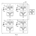
- FIG. 8 is a block diagram of a PLD in accordance with a voltage tuning embodiment of the invention.
- FIG. 9 is a block diagram of a PLD that implements variable voltage switching regulators in accordance with one embodiment of the invention.
- FIG. 10 is a circuit diagram of a level-shifting flip-flop for use in various embodiments of the present invention.
- unused and inactive resources in a programmable logic device are disabled to achieve lower static power consumption.
- PLD programmable logic device
- FPGA field programmable gate array
- the present invention includes both an enabling software flow and an enabling hardware architecture, which are described in more detail below.
- Unused resources of the PLD can be disabled when designing a particular circuit to be implemented by the PLD (hereinafter referred to as “design time”).
- design time a particular circuit to be implemented by the PLD
- resources of the PLD that are temporarily inactive can be disabled during operation of the PLD (hereinafter referred to as “run time”).
- FIG. 1 is a flow diagram 100 illustrating a conventional design flow used for PLDs.
- a user designs a circuit to be implemented by the PLD (Step 101 ).
- This user design is described in a high-level specification, such as Verilog or VHDL.
- the high-level specification is first synthesized to basic logic cells available on the PLD (Step 102 ).
- a place and route process then assigns every logic cell and wire in the design to some physical resource in the PLD (Step 103 ).
- the design is then converted into a configuration bit stream, in a manner known to those of ordinary skill in the art (Step 104 ).
- the configuration bit stream is then used to configure the device by setting various on-chip configuration memory cells (Step 105 ). While modern design flows may be much more complex, they all involve the basic steps defined by flow diagram 100 .
- unused resources of the PLD are identified during the design time, following the place and route process (Step 103 ). These unused resources are then selectively disabled during the design time. As described below, there are several ways to disable the unused resources. By selectively disabling the unused resources at design time, significant static power reduction may be achieved with no performance penalty.
- FIG. 2 is a flow diagram 200 illustrating a design flow in accordance with one embodiment of the present invention. Similar steps in flow diagrams 100 and 200 are labeled with similar reference numbers. Thus, flow diagram 200 includes Steps 101 – 105 of flow diagram 100 , which are described above. In addition, flow diagram 200 includes the step of disabling unused resources in the PLD (Step 201 ). This step of disabling unused resources is performed after the place and route process has been completed in Step 103 , and before the configuration bit stream is generated in Step 104 . As described in more detail below, the unused resources are disabled by disabling predetermined programmable logic blocks of the PLD.
- further power savings are obtained by disabling temporarily inactive resources of the configured PLD during run time.
- the entire design or parts of the design are temporarily inactive for some period of time. If the inactive period is sufficiently long, it is worthwhile to disable the inactive resources to reduce static power consumption.
- the decision of when to disable a temporarily inactive resource is made by the designer.
- the user logic is provided access to a disabling mechanism, which enables the inactive resources to be disabled dynamically.
- the PLD is logically subdivided into a plurality of separate programmable logic blocks.
- each programmable logic block may comprise one or more of the resources available on the programmable logic device.
- Switch elements are used to couple each of the programmable logic blocks to one or more associated voltage supply terminals (e.g., V DD or ground).
- the switch elements are controlled to perform a power-gating function, wherein unused and/or inactive programmable logic blocks are disabled (e.g., prevented from receiving power or receiving a reduced power).
- V DD or ground the voltage supply terminals
- the switch elements are controlled to de-couple the associated programmable logic blocks from the associated supply voltage, these programmable logic blocks are effectively disabled, thereby dramatically reducing the static power consumption of these blocks.
- FIG. 3 is a block diagram of a conventional PLD 300 having four programmable logic blocks 301 – 304 , which are all powered by the same off-chip V DD voltage supply 305 . Note that all four programmable logic blocks 301 – 304 are coupled to receive the V DD supply voltage during normal operating conditions, even if some of these blocks are not used in the circuit design.
- FIG. 4 is a block diagram of a PLD 400 in accordance with one embodiment of the present invention. Similar elements in FIGS. 3 and 4 are labeled with similar reference numbers.
- PLD 400 includes programmable logic blocks 301 – 304 and V DD voltage supply 305 .
- PLD 400 includes switch elements 401 – 408 , and control circuit 409 .
- switch elements 401 – 404 are implemented by PMOS power-gating transistors 451 – 454 , respectively, and switch elements 405 – 408 are implemented by NMOS power-gating transistors 455 – 458 , respectively.
- switch elements 401 – 408 may be any switch known to those ordinarily skilled in the art.
- Control circuit 409 is implemented by inverters 411 – 414 , NOR gates 421 – 424 , configuration memory cells 431 – 434 , and user logic input terminals 441 – 444 .
- NOR gates 421 – 424 and inverters 411 – 414 are configured to generate power-gating control signals SLEEP 1 –SLEEP 4 and SLEEP# 1 –SLEEP# 4 in response to the configuration data values CD 1 –CD 4 stored in configuration memory cells 431 – 434 , respectively, and the user control signals UC 1 –UC 4 provided on user logic input terminals 441 – 444 , respectively.
- NOR gate 421 is coupled to receive configuration data value CD 1 from configuration memory cell 431 and user control signal UC 1 from user logic input terminal 441 . If either the configuration data value CD 1 or the user control signal UC 1 is activated to a logic high state, then NOR gate 421 provides an output signal (SLEEP# 1 ) having a logic “0” state. In response, inverter 411 , which is coupled to the output terminal of NOR gate 421 , provides an output signal (SLEEP 1 ) having a logic “1” state.
- the SLEEP 1 signal is applied to the gate of PMOS power-gating transistor 451 , which is coupled between block 301 and the V DD voltage supply terminal.
- the SLEEP# 1 signal is applied to the gate of NMOS power-gating transistor 455 , which is coupled between block 301 and the ground voltage supply terminal.
- the logic “0” state of the SLEEP# 1 signal causes NMOS power-gating transistor 455 to turn off, thereby de-coupling block 301 from the ground supply voltage terminal.
- the logic “1” state of the SLEEP 1 signal causes PMOS power-gating transistor 451 to turn off, thereby de-coupling block 301 from the V DD supply voltage terminal. De-coupling block 301 from the V DD and ground supply voltage terminals effectively disables block 301 , thereby minimizing the static leakage current in this block.
- NOR gate 421 provides a SLEEP# 1 signal having a logic “1” state
- inverter 411 provides a SLEEP 1 signal having a logic “0” state.
- the logic “1” state of the SLEEP# 1 signal causes NMOS power-gating transistor 455 to turn on, thereby coupling block 301 to the ground supply voltage terminal.
- the logic “0” state of the SLEEP 1 signal causes PMOS power-gating transistor 451 to turn on, thereby coupling block 301 to the V DD supply voltage terminal. Coupling block 301 to the V DD and ground supply voltage terminals effectively enables block 301 .
- Programmable logic block 302 may be enabled and disabled in response to configuration data value CD 2 and user control signal UC 2 , in the same manner as block 301 .
- programmable logic block 303 may be enabled and disabled in response to configuration data value CD 3 and user control signal UC 3 , in the same manner as block 301 .
- Programmable logic block 304 may be enabled and disabled in response to configuration data value CD 4 and user control signal UC 4 , in the same manner as block 301 .
- SLEEP 1 —SLEEP 4 and SLEEP# 1 —SLEEP# 4 signals can be controlled by the configuration data values CD 1 –CD 4 stored by configuration memory cells 431 – 434 , which are best suited for disabling the associated blocks at design time. If a block is not disabled at design time, this block can be disabled at run time by the user control signals UC 1 –UC 4 , which may be generated by the user logic, or by other means.
- some blocks have multiple supply voltages. In this case all of the supply rails should be power-gated to achieve maximum power reduction.
- only one switch element may be associated with each block. That is, the blocks are power-gated by decoupling the block from only one power supply terminal, and not both the V DD and ground supply voltage terminals, thereby conserving layout area.
- each programmable logic block may be selected to include one or more configuration logic blocks (CLBs), input/output blocks (IOBs), and/or other resources of the FPGA (such as block RAM, processors, multipliers, adders, transceivers).
- CLBs configuration logic blocks
- IOBs input/output blocks
- other resources of the FPGA such as block RAM, processors, multipliers, adders, transceivers.
- Another way to disable a programmable logic block is by scaling down the local supply voltage to the block as low as possible, which dramatically reduces the power consumption of the block.
- each independently controlled programmable logic block is powered by a separate switching regulator.
- FIG. 5 is a block diagram of a PLD 500 that implements switching regulators in accordance with one embodiment of the present invention. Similar elements in FIGS. 3 and 5 are labeled with similar reference numbers.
- PLD 500 includes programmable logic blocks 301 – 304 and V DD voltage supply 305 .
- PLD 500 includes switching regulators 501 – 504 , which are coupled between blocks 301 – 304 , respectively, and V DD voltage supply 305 .
- Switching regulators 501 – 504 are controlled by control circuits 511 – 514 , respectively. In the described embodiment, switching regulators 501 – 504 reside on the same chip as blocks 301 – 304 .
- switching regulators 501 – 504 can be programmably tuned to provide the desired supply voltages to the associated programmable logic blocks 301 – 304 .
- switching regulator 501 can provide a full V DD supply voltage to programmable logic block 301 when this block is used and active.
- switching regulator 501 can further be controlled to provide a reduced voltage (e.g., some percentage of the V DD supply voltage) to programmable logic block 301 when this block is unused or inactive.
- This reduced voltage may be predetermined (by design or via testing) depending on the desired circuit behavior. For example, this reduced voltage may be the minimum voltage required to maintain the state of the associated blocks.
- the power consumption of block 301 is significantly reduced when the supplied voltage is reduced in this manner.
- Switching regulators 501 – 504 are controlled in response to the configuration data values C 1 –C 4 stored in configuration memory cells 511 – 514 , respectively, and the user control signals U 1 –U 4 provided on user control terminals 521 – 524 , respectively.
- a configuration data value e.g., C 1
- switching regulator 501 e.g., switching regulator 501
- the associated switching regulator e.g., switching regulator 501
- a user control signal (e.g., U 2 ) having an activated state will cause the associated switching regulator (e.g., switching regulator 502 ) to provide a reduced voltage to the associated programmable logic block (e.g., block 502 ).
- a configuration data value (e.g., C 3 ) and an associated user control signal (e.g., U 3 ) both having have deactivated states will cause the associated switching regulator (e.g., switching regulator 503 ) to provide the full V DD supply voltage to the associated programmable logic block (e.g., block 503 ).
- configuration data values C 1 –C 4 may be selected at design time, such that reduced voltages are subsequently applied to unused blocks during run time.
- User control signals U 1 –U 4 may be selected during run time, such that reduced voltages are dynamically applied to inactive blocks at run time.
- each programmable logic block 301 – 304 would most likely be divided into several clusters of configuration logic blocks (CLBs). The exact size of each programmable logic block may be determined by the desired trade-off among power savings, layout area overhead of the switching regulators, and the speed penalty.
- FIG. 6 is a block diagram of PLD 500 , which shows switching regulators 501 – 504 in accordance with one embodiment of the present invention.
- Switching regulators 501 – 504 include control blocks 601 – 604 , respectively, and high-voltage n-channel transistors 611 – 614 , respectively.
- High-voltage n-channel transistors 611 – 614 can tolerate high voltages and may have relatively thick gate dielectric layers (e.g., 50 to 60 Angstroms) and relatively wide channel regions.
- the gate dielectric thickness of the high-voltage n-channel transistors 611 – 614 is approximately 4 to 6 times thicker than the gate dielectric thickness used in the programmable logic blocks 301 – 304 .
- each of n-channel transistors 611 – 614 is coupled to the V DD voltage supply 305 .
- the gates of n-channel transistors 611 – 614 are coupled to receive the control voltages V C1 –V C4 , respectively, from the corresponding control blocks 601 – 604 .
- the source of each of n-channel transistors 611 – 614 is configured to provide an operating voltage V 1 –V 4 , respectively, to programmable logic blocks 301 – 304 , respectively.
- the source of each n-channel transistor 611 – 614 is also coupled to the corresponding control block 601 – 604 in a feedback configuration.
- Each of n-channel transistors 611 – 614 forms a power switch between the V DD supply voltage 305 and the associated programmable logic block.
- Thick oxide n-channel transistors 611 – 614 are used to implement the power switches to ensure that a high voltage, herein referred to as V BOOST , can be applied to the gates of n-channel transistors 611 – 614 when the associated programmable logic block is active.
- the high voltage V BOOST increases the drive current of n-channel transistors 611 – 614 .
- the high voltage V BOOST is about 2 to 2.5 times greater than V DD .
- the associated operating voltage (e.g., V 1 ) is reduced.
- the operating voltage applied to the associated programmable logic block is preferably selected to be high enough to retain data stored in this programmable logic block.
- the operating voltage is reduced to a voltage that is about one half the V DD supply voltage.
- the operating voltage is reduced by applying a low voltage V STANDBY to the gate of the corresponding n-channel transistor (e.g., transistor 611 ).
- the low voltage V STANDBY is about 80 to 100 percent of the V DD supply voltage.
- each of control blocks 601 – 604 is independently controlled to provide either the high voltage V BOOST or the low voltage V STANDBY to the associated n-channel transistor 611 – 614 .
- control block 601 is configured to receive the user control signal U 1 and the configuration data value C 1 , which have been described above. If both the user control signal U 1 and the configuration data value C 1 are deactivated, then control block 601 provides a control voltage V C1 equal to the high voltage V BOOST to the gate of n-channel transistor 611 . As a result, an operating voltage V 1 equal to the V DD supply voltage is applied to programmable logic block 301 .
- control block 601 provides a control voltage V C1 equal to the low voltage V STANDBY to the gate of n-channel transistor 611 .
- V C1 an operating voltage approximately equal to one half the V DD supply voltage is applied to programmable logic block 301 .
- control block 601 may include a feedback mechanism that adjusts the low voltage V STANDBY signal until the operating voltage V 1 is precisely equal to 1 ⁇ 2 V DD , or any other desired voltage.
- the gate current through a transistor typically increases by an order of magnitude for every 0.3 Volt increase in the V DD supply voltage. It is therefore expected that reducing the operating voltage of a programmable logic block by half (1 ⁇ 2 V DD ) will reduce the gate current through the transistors present in the programmable logic block by an order of magnitude or more. At the same time, the sub-threshold leakage of these transistors will also decrease with the reduced operating voltage. Based on earlier generation technology, the leakage current may be reduced by 70% or more when reducing the operating voltage to 1 ⁇ 2 V DD . Simulation of a ring oscillator shows that the ring oscillator will operate properly at the lower operating voltage (1 ⁇ 2 V DD ). It can be expected the associated logic block will retain stored data using the lower operating voltage. Therefore, the proposed switching regulators are capable of achieving more than 70% reduction in leakage current without a significant increase in area penalty and without sacrificing desired functionality.
- the operating voltages applied to different blocks of a PLD are tuned based on application-specific timing characteristics to achieve a more power-efficient design implementation. Both the hardware architecture necessary to enable the tuning and the software flow used to perform the tuning are described below.
- the tuning may be performed at design time to optimize resources that have timing slacks, or at runtime to exploit periods of low workload.
- Timable logic blocks with timing slacks are faster than what is necessary to meet the timing requirements of the PLD design. These blocks may be tuned to be slower, such that their timing slacks are reduced or eliminated, without negatively impacting the timing requirements of the overall design.
- the methods by which the programmable logic blocks are tuned also lower the power consumption of these blocks, thereby achieving a significant power reduction with no timing penalty. In essence, tuning the chip in this manner customizes the programmable logic device to meet the timing requirements of the PLD design, thereby resulting in a more power-efficient design mapping.
- FIG. 7 is a flow diagram 700 illustrating a design flow in accordance with the operating voltage tuning embodiment of the present invention. Similar steps in flow diagrams 100 and 700 are labeled with similar reference numbers. Thus, flow diagram 700 includes Steps 101 – 105 of flow diagram 100 , which are described above. In addition, flow diagram 700 includes the step of performing a timing analysis on the PLD design (Step 701 ). This timing analysis identifies the delays along various paths of the PLD design. This timing analysis may be performed after the place and route process has been completed in Step 103 .
- the timing slacks may be identified by comparing the expected delay of the path with the critical delay of the path. That is, the paths having timing slacks of N% or more of the critical delay are identified (Step 702 ). For example, in a synchronous design where the critical delay is 10 ns, all paths more than 20% faster than the critical delay are identified. As a result, all paths with delay of 8 ns or less are identified. These paths can all be slowed by at least 2 ns without impacting the timing of the overall design.
- the minimum operating voltage for each block is then determined (Step 703 ).
- a translation table is used (Step 704 ), wherein the translation table provides a minimum operating voltage in response to a particular timing slack. Note that for larger timing slacks, the minimum operating voltage will be lower.
- each independently tunable programmable logic block in the device is examined to determine the maximum amount of acceptable delay increase, which corresponds to the minimum timing slack among all of the paths in the programmable logic block (Step 703 ). Then, the minimum timing slack for each programmable logic block is converted to a minimum operating voltage by performing a lookup operation in a timing/voltage translation table (Step 704 ).
- the timing/voltage translation table can be populated via chip testing.
- the entries in the translation table may take the format of “X ns decrease in speed requires a supply voltage adjustment by Y Volts”.
- the configuration bit stream is generated in Step 104 .
- the configuration bit stream is generated such that the configuration bit stream applies the minimum operating voltages as determined in Step 704 .
- the minimum operating voltages can be applied by setting the supply voltages to various programmable logic blocks of the PLD in response to the configuration data bits.
- the PLD is then configured in response to the configuration bit stream (Step 105 ).
- an initial timing analysis is performed prior to the place and route operation (Step 103 ), based on estimated delays of the various paths.
- the place and route step is then guided to group paths with significant timing slacks in to the same independently tunable block.
- FIG. 8 is a block diagram of a PLD 800 in accordance with the present embodiment of the invention.
- PLD 800 includes programmable logic blocks 801 – 804 , high voltage (V DD — H) supply 805 , low voltage (V DD — L) supply 806 , control circuit 809 and switch elements 851 – 858 .
- switch elements 851 – 858 are implemented by PMOS power-gating transistors.
- Control circuit 809 is implemented by inverters 811 – 814 , NOR gates 821 – 824 , configuration memory cells 831 – 834 , and user logic input terminals 841 – 844 .
- the high voltage supply 805 is configured to provide a full V DD supply voltage, which is designated V DD — H.
- the low voltage supply 806 is configured to provide a reduced V DD supply voltage, which is designated V DD — L.
- the V DD — L supply voltage is less than the V DD — H supply voltage by a selected percentage. For example, the V DD — L supply voltage may be 80 percent of the V DD — H supply voltage.
- NOR gates 821 – 824 and inverters 811 – 814 are configured to generate the high voltage select signals Sel_H 1 –Sel_H 4 and the low voltage select signals Sel_L 1 –Sel_L 4 , in response to the configuration data values CD 1 –CD 4 stored in configuration memory cells 831 – 834 , respectively, and the user control signals UC 1 –UC 4 provided on user logic input terminals 841 – 844 , respectively.
- NOR gate 821 is coupled to receive configuration data value CD 1 from configuration memory cell 831 and user control signal UC 1 from user logic input terminal 841 . If either the configuration data value CD 1 or the user control signal UC 1 is activated to a logic high state (indicating that a substantial timing slack exists in programmable logic block 801 , and that the V DD — L voltage supply 806 should be coupled to this block 801 ), then NOR gate 821 provides a low voltage select signal Sel_L 1 having a logic “0” state. In response, inverter 811 , which is coupled to the output terminal of NOR gate 821 , provides a high voltage select signal Sel_H 1 having a logic “1” state.
- the logic “0” Sel_L 1 signal is applied to the gate of PMOS voltage select transistor 852 , thereby turning on this transistor and coupling programmable logic block 801 to the V DD— L voltage supply 806 .
- the logic “1” Sel_H 1 signal is applied to the gate of PMOS voltage select transistor 851 , thereby turning off this transistor and isolating programmable logic block 801 from the V DD— H voltage supply 805 .
- programmable logic block 801 operates in response to the V DD— L supply voltage, V DD— L, thereby minimizing the leakage current in this block.
- NOR gate 821 provides a low voltage select signal Sel_L 1 having a logic “1” state.
- inverter 811 provides a high voltage select signal Sel_H 1 having a logic “0” state.
- the logic “0” Sel_H 1 signal is applied to the gate of PMOS voltage select transistor 851 , thereby turning on this transistor and coupling programmable logic block 801 to the V DD— H voltage supply 805 .
- the logic “1” Sel_L 1 signal is applied to the gate of PMOS voltage select transistor 852 , thereby turning off this transistor and isolating programmable logic block 801 from the V DD— L voltage supply 806 .
- programmable logic block 801 operates in response to the V DD— H supply voltage, thereby enabling this block to operate at the required speed.
- Programmable logic block 802 is coupled to the V DD— H voltage supply 805 or the V DD— L voltage supply 806 in response to configuration data value CD 2 and user control signal UC 2 , in the same manner as block 801 .
- programmable logic block 803 is coupled to the V DD— H voltage supply 805 or the V DD— L voltage supply 806 in response to configuration data value CD 3 and user control signal UC 3 , in the same manner as block 801 .
- Programmable logic block 804 is coupled to the V DD— H voltage supply 805 or the V DD— L voltage supply 806 in response to configuration data value CD 4 and user control signal UC 4 , in the same manner as block 801 .
- the Sel_H 1 –Sel_H 4 and Sel_L 1 –Sel_L 4 signals can be controlled by the configuration data values CD 1 –CD 4 stored by configuration memory cells 831 – 834 , which are best suited for coupling the associated blocks to the V DD— L voltage supply 806 at design time. If a block is not coupled to the V DD — L voltage supply 806 at design time, this block can be coupled to the V DD— L voltage supply 806 at run time by the user control signals UC 1 –UC 4 , which may be generated by the user logic.
- a tunable programmable logic device is implemented by enabling local supply voltage scaling.
- each independently tunable programmable logic block is powered by a separate variable-voltage switching regulator.
- the programmable logic blocks are tuned by configuring the regulators to adjust the operating voltages applied to the programmable logic blocks. When the operating voltage of a programmable logic block is scaled down, the block becomes slower, and the dynamic and static power consumed by the block are dramatically reduced.
- FIG. 9 is a block diagram of a PLD 900 that implements variable voltage switching regulators in accordance with the present embodiment of the invention.
- PLD 900 includes programmable logic blocks 901 – 904 , V DD voltage supply 905 , configuration memory cell sets 911 – 914 , user control terminal sets 921 – 924 , and variable voltage switching regulators 931 – 934 .
- Voltage regulators 931 – 934 are configured to provide operating voltages to programmable logic blocks 901 – 904 , respectively, in response to the V DD supply voltage.
- Each of voltage regulators 931 – 934 independently may select one of two or more possible operating voltages in response to the configuration data bits stored in configuration memory cell sets 911 – 914 , respectively.
- voltage regulator 931 may provide operating voltages equal to V DD , 0.95V DD , 0.9V DD or 0.85 V DD in response to the configuration data bits stored in configuration memory cell set 911 .
- Other numbers of configuration memory cells and other operating voltages can be provided in other embodiments.
- PLD 900 dynamically (during runtime) to exploit variations in the application's workload or performance requirements.
- Many user designs go through periods of low workload, during which the affected blocks may be tuned to lower speed and lower power.
- the tuning is preferably initiated by the user design, since the user has the best knowledge of when extended periods of low workload will occur.
- One way to enable dynamic scaling of local voltages is through dynamic reconfiguration of the programmable regulators using techniques described by Brandon J. Blodget et al., “Reconfiguration of a Programmable Logic Device Using Internal Control,” U.S. patent application Ser. No. 10/377,857.
- the user may implement such an adjustment by varying the N signals provided on the user control terminal set 921 , or by rewriting the desired configuration memory bits into configuration memory cell set 911 .
- the other variable voltage switching regulators 932 – 934 are controlled in the same manner as voltage regulator 931 .
- variable voltage switching regulators 931 – 934 reside on the same chip as programmable logic blocks 901 – 904 . However, in other embodiments, these voltage regulators 931 – 934 can be located external to the chip containing blocks 901 – 904 .
- each programmable logic block 901 – 904 would most likely be divided into several clusters of configuration logic blocks (CLBs). The exact size of each programmable logic block is determined by the desired trade-off between power savings and the layout area overhead of the switching regulators.
- level-shifters should be used as interfacing logic. To reduce area and speed overhead, level-shifters can be integrated into flip-flops, which are typically present on the programmable logic device.
- FIG. 10 is a circuit diagram of a level-shifting flip-flop 1000 , for use in accordance with one embodiment of the present invention.
- Flip-flop 1000 includes inverters 1001 – 1004 , complementary pass gates 1011 – 1012 , p-channel transistors 1021 – 1022 , and n-channel transistors 1031 – 1034 .
- Inverters 1001 – 1003 and complementary pass gates 1011 – 1012 operate in response to the V DD — L supply voltage.
- CLK# signal is high (CLK is low)
- inverter 1001 is enabled to route the inverse of the input data value D to inverter 1002 .
- the input data value D is defined at the V DD — L voltage level.
- Inverter 1003 and complementary pass gates 1011 – 1012 are disabled by the low CLK signal at this time.
- inverter 1001 When the CLK signal transitions to a logic high state (CLK# is low), inverter 1001 is disabled and inverter 1003 is enabled, thereby allowing the data value D to be latched into cross-coupled inverters 1002 – 1003 .
- the logic low CLK# signal disables n-channel transistors 1033 and 1034 .
- the high CLK signal also enables complementary pass gates 1011 – 1012 , thereby applying the data value D and the inverse data value D# to the gates of n-channel transistors 1031 and 1032 , respectively. As a result, the data value D or the inverse data value D# turns on one of n-channel transistors 1031 or 1032 .
- n-channel transistor 1031 is turned off and n-channel transistor 1032 is turned on.
- Turned on transistor 1032 pulls down the gate voltage of p-channel transistor 1021 to ground, thereby turning on this transistor 1021 .
- Turned on transistor 1021 applies the V DD — H voltage to the gate of p-channel transistor 1022 (thereby turning this transistor off), and to the input terminal of inverter 1004 (which provides a logic low Q output signal). Note that the Q output signal has been translated to the V DD — H voltage level.
- Level-shifting flip flop 1000 is described in more detail by M. Takahashi et al., “A 60 mW MPEG4 Video Codec using Clustered Voltage Scaling with Variable Supply-Voltage Scheme,” Journal of Solid State Circuits, vol. 33, no. 11, pp. 1772–1780, November 1998.
Abstract
A method of operating a programmable logic device includes the steps of using a full VDD supply voltage to operate a first set of active blocks of the programmable logic device, and using a reduced supply voltage (e.g., 0.9 VDD) to operate a second set of active blocks of the programmable logic device. A timing analysis is performed to determine the maximum available timing slack in each active block. Active blocks having a smaller timing slack are grouped in the first set, and are coupled to receive the full VDD supply voltage. Active blocks having a larger timing slack are grouped in the second set, and are coupled to receive the reduced VDD supply voltage. As a result, the active blocks in the second set exhibit reduced power consumption, without adversely affecting the overall speed of the programmable logic device.
Description
The present application is a continuation-in-part of U.S. patent application Ser. No. 10/666,669 filed by Tim Tuan, Kameswara K. Rao and Robert O. Conn on Sep. 19, 2003 now U.S. Pat. No. 7,098,689, which is incorporated herein in its entirety.
The present invention relates to the regulation of the supply voltage provided to unused and/or inactive blocks in a programmable logic device to achieve lower power consumption. More specifically, the present invention relates to selectively reducing the operating voltage of various sections of an integrated circuit device in order to reduce the leakage current and/or increase the performance of the device.
Programmable logic devices (PLDs), such as field programmable gate arrays (FPGAs), have a significantly higher static power consumption than dedicated logic devices, such as standard-cell application specific integrated circuits (ASICs). A reason for this high static power consumption is that for any given design, a PLD only uses a subset of the available resources. The unused resources are necessary for providing greater mapping flexibility to the PLD. However, these unused resources still consume static power in the form of leakage current. Consequently, PLDs are generally less likely to be used in applications where low static power is required.
It would therefore be desirable to have a PLD having a reduced static power consumption.
Programmable logic devices (PLDs) also have a significantly higher dynamic power consumption than dedicated logic devices because the PLD resources (logic and routing) are designed with a fixed level of performance, regardless of the requirements of the specific application being implemented by the PLD. Most PLD applications do not require the maximum hardware speed for some (or even all) parts of the PLD. As a result, “timing slack” exists in different parts of the PLD. In fact, the timing critical part of a PLD design typically represents a very small portion of the whole design. In circuit design, higher speed circuits generally consume more power, both dynamic and static. Consequently, the parts of the PLD that are not operated at the maximum hardware speed represent an inefficient use of power.
It would therefore be desirable to improve the power efficiency of a programmable logic device by taking advantage of the timing slack present in different parts of a PLD design.
In accordance with one embodiment of the present invention, unused and/or inactive resources in a PLD are disabled to achieve lower power consumption.
One embodiment of the present invention provides a method of operating a PLD, which includes the steps of enabling the resources of the PLD that are used in a particular circuit design, and disabling the resources of the PLD that are unused or inactive. The step of disabling can include de-coupling the unused or inactive resources from one or more power supply terminals. Alternately, the step of disabling can include regulating (e.g., reducing) a supply voltage applied to the unused or inactive resources.
In accordance with one embodiment, the step of disabling can be performed in response to configuration data bits stored by the PLD. These configuration data bits can be determined during the design of the circuit to be implemented by the PLD. That is, during the design, the design software is able to identify unused resources of the PLD, and select the configuration data bits to disable these unused resources.
The step of disabling can also be performed in response to user-controlled signals. These user-controlled signals can be generated in response to observable operating conditions of the PLD. For example, if certain resources of the operating PLD are inactive for a predetermined time period, then the user-controlled signals may be activated, thereby causing the inactive resources to be disabled.
In accordance with another embodiment, a PLD includes a first voltage supply terminal that receives a first supply voltage, a plurality of programmable logic blocks, and a plurality of switch elements, wherein each switch element is coupled between one of the programmable logic blocks and the first voltage supply terminal. A control circuit coupled to the switch elements provides a plurality of control signals that selectively enable or disable the switch elements. The control circuit can be controlled by a plurality of configuration data values stored by the PLD and/or a plurality of user-controlled signals.
In an alternate embodiment, each of the switch elements can be replaced by a switching regulator. In this embodiment, the operating voltage applied to different blocks of the PLD may be adjusted in view of the timing slack available in these blocks. That is, a block with a large amount of timing slack can be operated at a lower voltage, thereby causing the block to operate at a slower speed, which is acceptable within the parameters of the PLD design. The lower operating voltage advantageously reduces the leakage current in the block. Blocks with a small amount of timing slack are operated at a higher voltage, thereby enabling these blocks to operate at the required high speed.
In accordance with one embodiment, the switching regulator can be a high-voltage n-channel transistor having a drain coupled to the VDD voltage supply and a source coupled to the programmable logic block. The gate of the high voltage transistor is coupled to receive a control voltage from a corresponding control circuit. The control circuit determines whether the corresponding programmable logic block is in an active or inactive state in response to user controlled signals and/or configuration data bits. When the programmable logic block is active, the control circuit applies a high control voltage VBOOST, which is greater than the VDD supply voltage, to the gate of the high voltage transistor, such that the full VDD supply voltage is applied to the programmable logic block. When the programmable logic block is inactive, the control circuit applies a low control voltage VSTANDBY, which is less than the VDD supply voltage, to the gate of the high voltage transistor, such that a voltage of about one half the VDD supply voltage is applied to the programmable logic block. A feedback mechanism can be employed to ensure that the voltage applied to the programmable logic block is precisely equal to one half the VDD supply voltage.
In accordance with another embodiment, a method of operating a programmable logic device includes the steps of using a full VDD supply voltage to operate a first set of active blocks of the programmable logic device, and using a reduced supply voltage (e.g., 0.9 VDD) to operate a second set of active blocks of the programmable logic device. A timing analysis is performed during design time and/or run time, in order to determine the maximum available timing slack in each active block. Active blocks having a relatively small timing slack are grouped in the first set, and are coupled to receive the full VDD supply voltage. As a result, the active blocks in the first set receive a voltage high enough to enable these blocks to meet the timing requirements of the PLD design.
Active blocks having a relatively large timing slack are grouped in the second set, and are coupled to receive the reduced VDD supply voltage. As a result, the active blocks in the second set exhibit reduced power consumption (as a result of operating in response to the reduced VDD supply voltage). In addition, the active blocks in the second set meet the timing requirements of the PLD design, in spite of operating in response to the reduced VDD supply voltage, because of the large timing slack initially present in these blocks. As a result, operating the active blocks in the second set at the reduced VDD supply voltage does not adversely affect the overall speed of the programmable logic device.
The reduced VDD supply voltage can be supplied in various manners, including, but not limited to, variable voltage switching regulators, or a separate voltage supply. The application of the full VDD voltage supply or the reduced VDD voltage supply can be controlled by configuration data bits and/or user control signals.
The present invention will be more fully understood in view of the following description and drawings.
In accordance with one embodiment of the present invention, unused and inactive resources in a programmable logic device (PLD), such as a field programmable gate array (FPGA), are disabled to achieve lower static power consumption. The present invention includes both an enabling software flow and an enabling hardware architecture, which are described in more detail below. Unused resources of the PLD can be disabled when designing a particular circuit to be implemented by the PLD (hereinafter referred to as “design time”). In addition, resources of the PLD that are temporarily inactive can be disabled during operation of the PLD (hereinafter referred to as “run time”).
In accordance with the present invention, unused resources of the PLD are identified during the design time, following the place and route process (Step 103). These unused resources are then selectively disabled during the design time. As described below, there are several ways to disable the unused resources. By selectively disabling the unused resources at design time, significant static power reduction may be achieved with no performance penalty.
In another embodiment, further power savings are obtained by disabling temporarily inactive resources of the configured PLD during run time. Often, the entire design or parts of the design are temporarily inactive for some period of time. If the inactive period is sufficiently long, it is worthwhile to disable the inactive resources to reduce static power consumption. In a preferred embodiment, the decision of when to disable a temporarily inactive resource is made by the designer. In this embodiment, the user logic is provided access to a disabling mechanism, which enables the inactive resources to be disabled dynamically.
There are a number of techniques to disable resources in a PLD. In accordance with one embodiment, the PLD is logically subdivided into a plurality of separate programmable logic blocks. As described below, each programmable logic block may comprise one or more of the resources available on the programmable logic device. Switch elements are used to couple each of the programmable logic blocks to one or more associated voltage supply terminals (e.g., VDD or ground). The switch elements are controlled to perform a power-gating function, wherein unused and/or inactive programmable logic blocks are disabled (e.g., prevented from receiving power or receiving a reduced power). Preferably, only one of the voltage supply terminals (VDD or ground) is power-gated, thereby reducing the speed and area penalties associated with the switch elements. When the switch elements are controlled to de-couple the associated programmable logic blocks from the associated supply voltage, these programmable logic blocks are effectively disabled, thereby dramatically reducing the static power consumption of these blocks.
NOR gates 421–424 and inverters 411–414 are configured to generate power-gating control signals SLEEP1–SLEEP4 and SLEEP#1–SLEEP#4 in response to the configuration data values CD1–CD4 stored in configuration memory cells 431–434, respectively, and the user control signals UC1–UC4 provided on user logic input terminals 441–444, respectively.
For example, NOR gate 421 is coupled to receive configuration data value CD1 from configuration memory cell 431 and user control signal UC1 from user logic input terminal 441. If either the configuration data value CD1 or the user control signal UC1 is activated to a logic high state, then NOR gate 421 provides an output signal (SLEEP#1) having a logic “0” state. In response, inverter 411, which is coupled to the output terminal of NOR gate 421, provides an output signal (SLEEP1) having a logic “1” state.
The SLEEP1 signal is applied to the gate of PMOS power-gating transistor 451, which is coupled between block 301 and the VDD voltage supply terminal. The SLEEP#1 signal is applied to the gate of NMOS power-gating transistor 455, which is coupled between block 301 and the ground voltage supply terminal. The logic “0” state of the SLEEP#1 signal causes NMOS power-gating transistor 455 to turn off, thereby de-coupling block 301 from the ground supply voltage terminal. Similarly, the logic “1” state of the SLEEP1 signal causes PMOS power-gating transistor 451 to turn off, thereby de-coupling block 301 from the VDD supply voltage terminal. De-coupling block 301 from the VDD and ground supply voltage terminals effectively disables block 301, thereby minimizing the static leakage current in this block.
If both the configuration data value CD1 and the user control signal UC1 are de-activated to a logic low state, then NOR gate 421 provides a SLEEP#1 signal having a logic “1” state, and inverter 411 provides a SLEEP1 signal having a logic “0” state. The logic “1” state of the SLEEP#1 signal causes NMOS power-gating transistor 455 to turn on, thereby coupling block 301 to the ground supply voltage terminal. Similarly, the logic “0” state of the SLEEP1 signal causes PMOS power-gating transistor 451 to turn on, thereby coupling block 301 to the VDD supply voltage terminal. Coupling block 301 to the VDD and ground supply voltage terminals effectively enables block 301.
As described above, when a programmable logic block is used and active, the associated power-gating transistors are turned on. Conversely, when a programmable logic block is unused or inactive, the associated power gating transistors are turned off. The SLEEP1—SLEEP4 and SLEEP#1—SLEEP#4 signals can be controlled by the configuration data values CD1–CD4 stored by configuration memory cells 431–434, which are best suited for disabling the associated blocks at design time. If a block is not disabled at design time, this block can be disabled at run time by the user control signals UC1–UC4, which may be generated by the user logic, or by other means.
In accordance with another embodiment of the present invention, some blocks have multiple supply voltages. In this case all of the supply rails should be power-gated to achieve maximum power reduction. In accordance with another embodiment, only one switch element may be associated with each block. That is, the blocks are power-gated by decoupling the block from only one power supply terminal, and not both the VDD and ground supply voltage terminals, thereby conserving layout area.
The granularity of the power-gated programmable logic blocks can range from arbitrarily small circuits to significant portions of the PLD. The decision concerning the size of each programmable logic block is made by determining the desired trade-off between power savings, layout area overhead of the switch elements and the control circuit, and speed penalty. In a FPGA, each programmable logic block may be selected to include one or more configuration logic blocks (CLBs), input/output blocks (IOBs), and/or other resources of the FPGA (such as block RAM, processors, multipliers, adders, transceivers).
Another way to disable a programmable logic block is by scaling down the local supply voltage to the block as low as possible, which dramatically reduces the power consumption of the block. To scale down the local supply voltage in this manner, each independently controlled programmable logic block is powered by a separate switching regulator.
In accordance with one embodiment, configuration data values C1–C4 may be selected at design time, such that reduced voltages are subsequently applied to unused blocks during run time. User control signals U1–U4 may be selected during run time, such that reduced voltages are dynamically applied to inactive blocks at run time. Techniques for distributing multiple programmable down-converted voltages using on-chip switching voltage regulators are described in more detail in U.S. patent application Ser. No. 10/606,619, “Integrated Circuit with High-Voltage, Low-Current Power Supply Distribution and Methods of Using the Same” by Bernard J. New et al., which is hereby incorporated by reference.
In the embodiment of FIG. 5 , the granularity of the voltage scaled programmable logic blocks 301–304 should be fairly large because the overhead associated with switching regulators 501–504 is significant. In an FPGA, each programmable logic block 301–304 would most likely be divided into several clusters of configuration logic blocks (CLBs). The exact size of each programmable logic block may be determined by the desired trade-off among power savings, layout area overhead of the switching regulators, and the speed penalty.
Each of n-channel transistors 611–614 forms a power switch between the VDD supply voltage 305 and the associated programmable logic block. Thick oxide n-channel transistors 611–614 are used to implement the power switches to ensure that a high voltage, herein referred to as VBOOST, can be applied to the gates of n-channel transistors 611–614 when the associated programmable logic block is active. The high voltage VBOOST increases the drive current of n-channel transistors 611–614. In accordance with one embodiment, the high voltage VBOOST is about 2 to 2.5 times greater than VDD. When the high voltage VBOOST is applied to the gate of one of transistors 611–614, the corresponding operating voltage V1–V4 is pulled up to the full VDD supply voltage.
When a programmable logic block (e.g., programmable logic block 301) is inactive, the associated operating voltage (e.g., V1) is reduced. The operating voltage applied to the associated programmable logic block is preferably selected to be high enough to retain data stored in this programmable logic block. In one embodiment, the operating voltage is reduced to a voltage that is about one half the VDD supply voltage. The operating voltage is reduced by applying a low voltage VSTANDBY to the gate of the corresponding n-channel transistor (e.g., transistor 611). In one embodiment, the low voltage VSTANDBY is about 80 to 100 percent of the VDD supply voltage.
In accordance with one embodiment, each of control blocks 601–604 is independently controlled to provide either the high voltage VBOOST or the low voltage VSTANDBY to the associated n-channel transistor 611–614.
For example, control block 601 is configured to receive the user control signal U1 and the configuration data value C1, which have been described above. If both the user control signal U1 and the configuration data value C1 are deactivated, then control block 601 provides a control voltage VC1 equal to the high voltage VBOOST to the gate of n-channel transistor 611. As a result, an operating voltage V1 equal to the VDD supply voltage is applied to programmable logic block 301.
However, if either user control signal U1 or configuration data value C1 is activated, then control block 601 provides a control voltage VC1 equal to the low voltage VSTANDBY to the gate of n-channel transistor 611. As a result, an operating voltage V1 approximately equal to one half the VDD supply voltage is applied to programmable logic block 301.
To ensure that the operating voltage V1 applied to programmable logic block 301 has a value of ½ VDD when the VSTANDBY voltage is applied to the gate of transistor 611, the control block 601 may include a feedback mechanism that adjusts the low voltage VSTANDBY signal until the operating voltage V1 is precisely equal to ½ VDD, or any other desired voltage.
It is well known that the gate current through a transistor typically increases by an order of magnitude for every 0.3 Volt increase in the VDD supply voltage. It is therefore expected that reducing the operating voltage of a programmable logic block by half (½ VDD) will reduce the gate current through the transistors present in the programmable logic block by an order of magnitude or more. At the same time, the sub-threshold leakage of these transistors will also decrease with the reduced operating voltage. Based on earlier generation technology, the leakage current may be reduced by 70% or more when reducing the operating voltage to ½ VDD. Simulation of a ring oscillator shows that the ring oscillator will operate properly at the lower operating voltage (½ VDD). It can be expected the associated logic block will retain stored data using the lower operating voltage. Therefore, the proposed switching regulators are capable of achieving more than 70% reduction in leakage current without a significant increase in area penalty and without sacrificing desired functionality.
In accordance with yet another embodiment of the present invention, the operating voltages applied to different blocks of a PLD are tuned based on application-specific timing characteristics to achieve a more power-efficient design implementation. Both the hardware architecture necessary to enable the tuning and the software flow used to perform the tuning are described below. The tuning may be performed at design time to optimize resources that have timing slacks, or at runtime to exploit periods of low workload.
It can be determined at design time, after the place and route steps, which parts of the PLD design have timing slacks. Programmable logic blocks with timing slacks are faster than what is necessary to meet the timing requirements of the PLD design. These blocks may be tuned to be slower, such that their timing slacks are reduced or eliminated, without negatively impacting the timing requirements of the overall design. The methods by which the programmable logic blocks are tuned also lower the power consumption of these blocks, thereby achieving a significant power reduction with no timing penalty. In essence, tuning the chip in this manner customizes the programmable logic device to meet the timing requirements of the PLD design, thereby resulting in a more power-efficient design mapping.
After the timing analysis is complete, all paths having significant timing slacks are identified along with the amount of slacks they possess. In one embodiment, the timing slacks may be identified by comparing the expected delay of the path with the critical delay of the path. That is, the paths having timing slacks of N% or more of the critical delay are identified (Step 702). For example, in a synchronous design where the critical delay is 10 ns, all paths more than 20% faster than the critical delay are identified. As a result, all paths with delay of 8 ns or less are identified. These paths can all be slowed by at least 2 ns without impacting the timing of the overall design.
The minimum operating voltage for each block is then determined (Step 703). In accordance with one embodiment, a translation table is used (Step 704), wherein the translation table provides a minimum operating voltage in response to a particular timing slack. Note that for larger timing slacks, the minimum operating voltage will be lower.
Following the identification of paths with significant timing slacks, each independently tunable programmable logic block in the device is examined to determine the maximum amount of acceptable delay increase, which corresponds to the minimum timing slack among all of the paths in the programmable logic block (Step 703). Then, the minimum timing slack for each programmable logic block is converted to a minimum operating voltage by performing a lookup operation in a timing/voltage translation table (Step 704). The timing/voltage translation table can be populated via chip testing. The entries in the translation table may take the format of “X ns decrease in speed requires a supply voltage adjustment by Y Volts”.
After the minimum operating voltage for each programmable logic block has been determined, the configuration bit stream is generated in Step 104. The configuration bit stream is generated such that the configuration bit stream applies the minimum operating voltages as determined in Step 704. As described in more detail below, the minimum operating voltages can be applied by setting the supply voltages to various programmable logic blocks of the PLD in response to the configuration data bits. The PLD is then configured in response to the configuration bit stream (Step 105).
In an enhanced version of the above-described embodiment, an initial timing analysis is performed prior to the place and route operation (Step 103), based on estimated delays of the various paths. The place and route step is then guided to group paths with significant timing slacks in to the same independently tunable block.
NOR gates 821–824 and inverters 811–814 are configured to generate the high voltage select signals Sel_H1–Sel_H4 and the low voltage select signals Sel_L1–Sel_L4, in response to the configuration data values CD1–CD4 stored in configuration memory cells 831–834, respectively, and the user control signals UC1–UC4 provided on user logic input terminals 841–844, respectively.
For example, NOR gate 821 is coupled to receive configuration data value CD1 from configuration memory cell 831 and user control signal UC1 from user logic input terminal 841. If either the configuration data value CD1 or the user control signal UC1 is activated to a logic high state (indicating that a substantial timing slack exists in programmable logic block 801, and that the VDD — L voltage supply 806 should be coupled to this block 801), then NOR gate 821 provides a low voltage select signal Sel_L1 having a logic “0” state. In response, inverter 811, which is coupled to the output terminal of NOR gate 821, provides a high voltage select signal Sel_H1 having a logic “1” state.
The logic “0” Sel_L1 signal is applied to the gate of PMOS voltage select transistor 852, thereby turning on this transistor and coupling programmable logic block 801 to the VDD— L voltage supply 806. The logic “1” Sel_H1 signal is applied to the gate of PMOS voltage select transistor 851, thereby turning off this transistor and isolating programmable logic block 801 from the VDD— H voltage supply 805. As a result, programmable logic block 801 operates in response to the VDD—L supply voltage, VDD—L, thereby minimizing the leakage current in this block.
If both the configuration data value CD1 and the user control signal UC1 are de-activated to a logic low state, (indicating that no substantial timing slack exists in programmable logic block 801, and that the VDD — H voltage supply 805 should be coupled to this block 801), then NOR gate 821 provides a low voltage select signal Sel_L1 having a logic “1” state. In response, inverter 811 provides a high voltage select signal Sel_H1 having a logic “0” state.
The logic “0” Sel_H1 signal is applied to the gate of PMOS voltage select transistor 851, thereby turning on this transistor and coupling programmable logic block 801 to the VDD— H voltage supply 805. The logic “1” Sel_L1 signal is applied to the gate of PMOS voltage select transistor 852, thereby turning off this transistor and isolating programmable logic block 801 from the VDD— L voltage supply 806. As a result, programmable logic block 801 operates in response to the VDD—H supply voltage, thereby enabling this block to operate at the required speed.
The Sel_H1–Sel_H4 and Sel_L1–Sel_L4 signals can be controlled by the configuration data values CD1–CD4 stored by configuration memory cells 831–834, which are best suited for coupling the associated blocks to the VDD— L voltage supply 806 at design time. If a block is not coupled to the VDD — L voltage supply 806 at design time, this block can be coupled to the VDD— L voltage supply 806 at run time by the user control signals UC1–UC4, which may be generated by the user logic.
In accordance with another embodiment, a tunable programmable logic device is implemented by enabling local supply voltage scaling. In this scheme, each independently tunable programmable logic block is powered by a separate variable-voltage switching regulator. The programmable logic blocks are tuned by configuring the regulators to adjust the operating voltages applied to the programmable logic blocks. When the operating voltage of a programmable logic block is scaled down, the block becomes slower, and the dynamic and static power consumed by the block are dramatically reduced.
It is further possible to tune PLD 900 dynamically (during runtime) to exploit variations in the application's workload or performance requirements. Many user designs go through periods of low workload, during which the affected blocks may be tuned to lower speed and lower power. The tuning is preferably initiated by the user design, since the user has the best knowledge of when extended periods of low workload will occur. One way to enable dynamic scaling of local voltages is through dynamic reconfiguration of the programmable regulators using techniques described by Brandon J. Blodget et al., “Reconfiguration of a Programmable Logic Device Using Internal Control,” U.S. patent application Ser. No. 10/377,857.
In accordance with one embodiment, the user may implement such an adjustment by varying the N signals provided on the user control terminal set 921, or by rewriting the desired configuration memory bits into configuration memory cell set 911. The other variable voltage switching regulators 932–934 are controlled in the same manner as voltage regulator 931.
In the described embodiment, variable voltage switching regulators 931–934 reside on the same chip as programmable logic blocks 901–904. However, in other embodiments, these voltage regulators 931–934 can be located external to the chip containing blocks 901–904.
Moreover, although the examples illustrate a PLD divided into four blocks, it should be understood that the PLD can be divided into arbitrary number of blocks, and each block can be of arbitrary granularity. In the embodiment of FIG. 9 , the granularity of the voltage scaled programmable logic blocks 901–904 should be fairly large because the overhead associated with variable voltage switching regulators 931–934 is significant. In an FPGA, each programmable logic block 901–904 would most likely be divided into several clusters of configuration logic blocks (CLBs). The exact size of each programmable logic block is determined by the desired trade-off between power savings and the layout area overhead of the switching regulators. Techniques for distributing multiple programmable voltages by using on-chip switching voltage regulators are described by Bernard J. New et al., in “Integrated Circuit With High-Voltage, Low-Current Power Supply Distribution And Methods Of Using The Same,” U.S. patent application Ser. No. 10/606,619.
Communication across programmable logic blocks having different operating voltages does not require special attention if the voltage difference is relatively small. However, when signals propagate from a low voltage block to a high voltage block, even small voltage differences can lead to significant DC current leakage in the high-voltage block due to transistors that are not completely turned off. To eliminate such DC current leakage, and to facilitate communication across two blocks of arbitrarily different voltages, level-shifters should be used as interfacing logic. To reduce area and speed overhead, level-shifters can be integrated into flip-flops, which are typically present on the programmable logic device.
When the CLK signal transitions to a logic high state (CLK# is low), inverter 1001 is disabled and inverter 1003 is enabled, thereby allowing the data value D to be latched into cross-coupled inverters 1002–1003. The logic low CLK# signal disables n- channel transistors 1033 and 1034. The high CLK signal also enables complementary pass gates 1011–1012, thereby applying the data value D and the inverse data value D# to the gates of n- channel transistors 1031 and 1032, respectively. As a result, the data value D or the inverse data value D# turns on one of n- channel transistors 1031 or 1032. For example, if the data value D has a logic low state, then n-channel transistor 1031 is turned off and n-channel transistor 1032 is turned on. Turned on transistor 1032 pulls down the gate voltage of p-channel transistor 1021 to ground, thereby turning on this transistor 1021. Turned on transistor 1021 applies the VDD — H voltage to the gate of p-channel transistor 1022 (thereby turning this transistor off), and to the input terminal of inverter 1004 (which provides a logic low Q output signal). Note that the Q output signal has been translated to the VDD — H voltage level. When the CLK signal transitions to a logic low state (CLK# is high), the n-channel transistors 1033–1034 turn on, thereby latching the data value D until the next rising edge of the CLK signal. Level-shifting flip flop 1000 is described in more detail by M. Takahashi et al., “A 60 mW MPEG4 Video Codec using Clustered Voltage Scaling with Variable Supply-Voltage Scheme,” Journal of Solid State Circuits, vol. 33, no. 11, pp. 1772–1780, November 1998.
Although the invention has been described in connection with several embodiments, it is understood that this invention is not limited to the embodiments disclosed, but is capable of various modifications, which would be apparent to a person skilled in the art. For example, although the described embodiments included four programmable logic blocks, it is understood that other numbers of blocks can be used in other embodiments. Thus, the invention is limited only by the following claims.
Claims (19)
1. A method of operating a programmable logic device comprising:
performing a timing analysis of a design of the programmable logic device having a plurality of active blocks, each active block of the plurality of active blocks having a plurality of paths;
determining a plurality of timing slacks associated with a plurality of paths of an active block for each of the plurality of active blocks of the design;
determining a minimum timing slack for each of the plurality of active blocks of the design;
enabling, for each active block of the plurality of active blocks, the assignment of either of a first supply voltage or a second supply voltage to operate an active block;
assigning the first supply voltage to operate a first set of one or more active blocks of the programmable logic device, the first supply voltage corresponding to the minimum timing slack determined for each active block in the first set; and
assigning the second supply voltage, less than the first supply voltage, to operate a second set of one or more active blocks of the programmable logic device, the second supply voltage corresponding to the minimum timing slack determined for each active block in the second set, wherein minimum timing slacks determined for each active block in the first set are less than minimum timing slacks determined for each active block in the second set.
2. The method of claim 1 , wherein the steps of assigning the first supply voltage and assigning the second supply voltage are performed in response to configuration data values stored during configuration of the programmable logic device.
3. The method of claim 1 , wherein the steps of assigning the first supply voltage and assigning the second supply voltage are performed in response to user controlled signals provided during run time of the programmable logic device.
4. The method of claim 3 , further comprising generating the user controlled signals in response to operating conditions of the programmable logic device during run time.
5. The method of claim 1 , wherein the steps of assigning the first supply voltage and assigning the second supply voltage are performed in response to configuration data values stored during run time of the programmable logic device.
6. The method of claim 1 , further comprising assigning a third supply voltage, less than the second supply voltage, to operate a third set of one or more active blocks of the programmable logic device, wherein timing slacks of the third set of one or more active blocks are greater than timing slacks of the first and second sets of one or more active blocks.
7. The method of claim 1 , further comprising:
identifying the first set of one or more active blocks as active blocks in the design having timing slacks less than a threshold timing slack; and
identifying the second set of one or more active blocks as active blocks in the design having timing slacks greater than the threshold timing slack.
8. The method of claim 1 , further comprising generating a configuration bit stream in response to the steps of assigning the first supply voltage and assigning the second supply voltage.
9. The method of claim 8 , further comprising, configuring the programmable logic device in response to the configuration bit stream.
10. The method of claim 1 , further comprising selecting the first set of one or more active blocks and the second set of one or more active blocks in response to the step of determining timing slacks.
11. The method of claim 1 , further comprising selecting the second voltage supply to be a minimum voltage required to maintain functionality of the second set of one or more active blocks.
12. A programmable logic device comprising:
a voltage supply terminal configured to receive a supply voltage;
a plurality of programmable logic blocks, each having an associated minimum timing slack determined from a corresponding plurality of timing slacks associated with a plurality of paths of a programmable logic block and receiving a selected one of a plurality of operating voltages;
a plurality of variable voltage regulators, each coupled between the voltage supply terminal and a corresponding one of the programmable logic blocks and selecting one of the plurality of operating voltages for the corresponding one of the programmable logic blocks; and
means for controlling the variable voltage regulators such that each of the variable voltage regulators provides an operating voltage to the corresponding one of the programmable logic blocks, wherein the operating voltage is selected in response to the minimum timing slack associated with the corresponding one of the programmable logic blocks.
13. The programmable logic device of claim 12 , wherein the means for controlling comprises one or more configuration memory cells coupled to each of the variable voltage regulators.
14. The programmable logic device of claim 12 , wherein the means for controlling comprises one or more user input terminals coupled to each variable voltage regulator.
15. The programmable logic device of claim 12 , further comprising a plurality of level shifters coupled among the plurality of programmable logic blocks.
16. A programmable logic device comprising:
a first voltage supply terminal configured to receive a first supply voltage;
a second voltage supply terminal configured to receive a second supply voltage, less than the first supply voltage;
a plurality of programmable logic blocks, each having an associated minimum timing slack determined from a corresponding plurality of timing slacks associated with a plurality of paths of the programmable logic block;
a plurality of first voltage switches, each coupled between the first voltage supply terminal and a corresponding one of the programmable logic blocks;
a plurality of second voltage switches, each coupled between the second voltage supply terminal and a corresponding one of the programmable logic blocks; and
means for controlling the first and second voltage switches such that each of the programmable logic blocks is coupled to receive one of the first voltage supply and the second voltage supply, wherein each of the programmable logic blocks having an associated minimum timing slack less than a threshold timing slack is coupled to receive the first supply voltage, and each of the programmable logic blocks having an associated minimum timing slack greater than the threshold timing slack is coupled to receive the second supply voltage.
17. The programmable logic device of claim 16 , wherein the means for controlling comprises one or more configuration memory cells coupled to the first and second voltage switches.
18. The programmable logic device of claim 16 , wherein the means for controlling comprises one or more user input terminals coupled to the first and second voltage switches.
19. The programmable logic device of claim 16 , further comprising a plurality of level shifters coupled among the plurality of programmable logic blocks.
Priority Applications (1)
| Application Number | Priority Date | Filing Date | Title |
|---|---|---|---|
| US10/783,216 US7549139B1 (en) | 2003-09-19 | 2004-02-20 | Tuning programmable logic devices for low-power design implementation |
Applications Claiming Priority (2)
| Application Number | Priority Date | Filing Date | Title |
|---|---|---|---|
| US10/666,669 US7098689B1 (en) | 2003-09-19 | 2003-09-19 | Disabling unused/inactive resources in programmable logic devices for static power reduction |
| US10/783,216 US7549139B1 (en) | 2003-09-19 | 2004-02-20 | Tuning programmable logic devices for low-power design implementation |
Related Parent Applications (1)
| Application Number | Title | Priority Date | Filing Date |
|---|---|---|---|
| US10/666,669 Continuation-In-Part US7098689B1 (en) | 2003-09-19 | 2003-09-19 | Disabling unused/inactive resources in programmable logic devices for static power reduction |
Publications (1)
| Publication Number | Publication Date |
|---|---|
| US7549139B1 true US7549139B1 (en) | 2009-06-16 |
Family
ID=40748674
Family Applications (1)
| Application Number | Title | Priority Date | Filing Date |
|---|---|---|---|
| US10/783,216 Active 2024-06-14 US7549139B1 (en) | 2003-09-19 | 2004-02-20 | Tuning programmable logic devices for low-power design implementation |
Country Status (1)
| Country | Link |
|---|---|
| US (1) | US7549139B1 (en) |
Cited By (13)
| Publication number | Priority date | Publication date | Assignee | Title |
|---|---|---|---|---|
| US20090299721A1 (en) * | 2005-12-21 | 2009-12-03 | Altera Corporation | Apparatus and methods for modeling power characteristics of electronic circuitry |
| US8130027B1 (en) * | 2009-01-22 | 2012-03-06 | Xilinx, Inc. | Apparatus and method for the detection and compensation of integrated circuit performance variation |
| US8159263B1 (en) | 2010-04-29 | 2012-04-17 | Xilinx, Inc. | Programmable integrated circuit with voltage domains |
| US20120216166A1 (en) * | 2011-02-18 | 2012-08-23 | Renesas Electronics Corporation | Layout method of semiconductor integrated circuit and program therefor |
| US8525546B1 (en) | 2012-03-08 | 2013-09-03 | International Business Machines Corporation | Majority dominant power scheme for repeated structures and structures thereof |
| US8823405B1 (en) | 2010-09-10 | 2014-09-02 | Xilinx, Inc. | Integrated circuit with power gating |
| US20140258956A1 (en) * | 2004-05-19 | 2014-09-11 | Altera Corporation | Apparatus and methods for power management in integrated circuits |
| US8918657B2 (en) | 2008-09-08 | 2014-12-23 | Virginia Tech Intellectual Properties | Systems, devices, and/or methods for managing energy usage |
| US20150256161A1 (en) * | 2014-03-07 | 2015-09-10 | Semiconductor Energy Laboratory Co., Ltd. | Method for driving semiconductor device |
| US9178518B2 (en) | 2010-03-17 | 2015-11-03 | University Of Virginia Patent Foundation | Sub-threshold FPGA and related circuits and methods thereof |
| US9419624B2 (en) | 2014-11-12 | 2016-08-16 | Xilinx, Inc. | Power management system for integrated circuits |
| US9513658B2 (en) | 2015-03-09 | 2016-12-06 | Apple Inc. | Multi-bit flip-flop reorganization techniques |
| US10333521B2 (en) | 2016-05-13 | 2019-06-25 | Semiconductor Energy Laboratory Co., Ltd. | Semiconductor device |
Citations (57)
| Publication number | Priority date | Publication date | Assignee | Title |
|---|---|---|---|---|
| US4962341A (en) | 1988-02-02 | 1990-10-09 | Schoeff John A | Low voltage non-saturating logic circuit technology |
| US5303390A (en) | 1990-06-28 | 1994-04-12 | Dallas Semiconductor Corporation | Microprocessor auxiliary with combined pin for reset output and pushbutton input |
| US5362989A (en) | 1992-12-16 | 1994-11-08 | Alliedsignal Inc. | Electrical isolation for power-saving purposes |
| US5519663A (en) | 1994-09-28 | 1996-05-21 | Sci Systems, Inc. | Preservation system for volatile memory with nonvolatile backup memory |
| US5568062A (en) | 1995-07-14 | 1996-10-22 | Kaplinsky; Cecil H. | Low noise tri-state output buffer |
| US5583457A (en) | 1992-04-14 | 1996-12-10 | Hitachi, Ltd. | Semiconductor integrated circuit device having power reduction mechanism |
| US5612892A (en) * | 1993-12-16 | 1997-03-18 | Intel Corporation | Method and structure for improving power consumption on a component while maintaining high operating frequency |
| US5615162A (en) | 1995-01-04 | 1997-03-25 | Texas Instruments Incorporated | Selective power to memory |
| US5671149A (en) | 1995-01-11 | 1997-09-23 | Dell Usa, L.P. | Programmable board mounted voltage regulators |
| US5682107A (en) | 1994-04-01 | 1997-10-28 | Xilinx, Inc. | FPGA architecture with repeatable tiles including routing matrices and logic matrices |
| US5712790A (en) * | 1995-04-11 | 1998-01-27 | International Business Machines Corporation | Method of power reduction in pla's |
| US5801548A (en) | 1996-04-11 | 1998-09-01 | Xilinx Inc | Configurable performance-optimized programmable logic device |
| US5811962A (en) | 1997-02-27 | 1998-09-22 | International Business Machines Corporation | Power supply control circuit |
| US5825662A (en) * | 1995-08-18 | 1998-10-20 | Xilinx, Inc. | Computer-implemented method of optimizing a time multiplexed programmable logic device |
| US5832286A (en) | 1991-12-04 | 1998-11-03 | Sharp Kabushiki Kaisha | Power control apparatus for digital electronic device |
| US5914873A (en) | 1997-06-30 | 1999-06-22 | Advanced Micro Devices | Distributed voltage converter apparatus and method for high power microprocessor with array connections |
| US5946257A (en) | 1996-07-24 | 1999-08-31 | Micron Technology, Inc. | Selective power distribution circuit for an integrated circuit |
| US5958026A (en) | 1997-04-11 | 1999-09-28 | Xilinx, Inc. | Input/output buffer supporting multiple I/O standards |
| US6038386A (en) * | 1997-08-21 | 2000-03-14 | Xilinx, Inc. | Method for controlling power and slew in a programmable logic device |
| US6114843A (en) | 1998-08-18 | 2000-09-05 | Xilinx, Inc. | Voltage down converter for multiple voltage levels |
| US6148390A (en) | 1996-06-12 | 2000-11-14 | Quicklogic Corporation | Techniques and circuits for high yield improvements in programmable devices using redundant logic |
| US6160418A (en) | 1999-01-14 | 2000-12-12 | Xilinx, Inc. | Integrated circuit with selectively disabled logic blocks |
| US6169419B1 (en) | 1998-09-10 | 2001-01-02 | Intel Corporation | Method and apparatus for reducing standby leakage current using a transistor stack effect |
| US6172518B1 (en) | 1999-07-23 | 2001-01-09 | Xilinx, Inc. | Method of minimizing power use in programmable logic devices |
| US6208171B1 (en) | 1998-04-20 | 2001-03-27 | Nec Corporation | Semiconductor integrated circuit device with low power consumption and simple manufacturing steps |
| US6384626B2 (en) | 2000-07-19 | 2002-05-07 | Micro-Star Int'l Co., Ltd. | Programmable apparatus and method for programming a programmable device |
| US6466049B1 (en) | 2000-09-14 | 2002-10-15 | Xilinx, Inc. | Clock enable control circuit for flip flops |
| US6489804B1 (en) | 2001-06-01 | 2002-12-03 | Sun Microsystems, Inc. | Method for coupling logic blocks using low threshold pass transistors |
| US20030030326A1 (en) | 2001-08-10 | 2003-02-13 | Shakti Systems, Inc. | Distributed power and supply architecture |
| US6583645B1 (en) | 2001-08-27 | 2003-06-24 | Xilinx, Inc. | Field programmable optical arrays |
| US6631502B2 (en) | 2002-01-16 | 2003-10-07 | International Business Machines Corporation | Method of analyzing integrated circuit power distribution in chips containing voltage islands |
| US20030218478A1 (en) | 2002-05-24 | 2003-11-27 | Sani Mehdi Hamidi | Regulation of crowbar current in circuits employing footswitches/headswitches |
| US6711719B2 (en) | 2001-08-13 | 2004-03-23 | International Business Machines Corporation | Method and apparatus for reducing power consumption in VLSI circuit designs |
| US6710621B2 (en) | 2001-02-16 | 2004-03-23 | Nallatech, Ltd. | Programmable power supply for field programmable gate array modules |
| US6747478B2 (en) | 2002-07-08 | 2004-06-08 | Viciciv | Field programmable gate array with convertibility to application specific integrated circuit |
| US20040145955A1 (en) * | 1999-10-14 | 2004-07-29 | Renesas Technology Corporation | Semiconductor device |
| US6839888B2 (en) | 2001-01-31 | 2005-01-04 | Stmicroelectronics, Inc. | Method for implementing bit-swap functions in a field programmable gate array |
| US6885563B2 (en) | 2001-09-26 | 2005-04-26 | Molex Incorporated | Power delivery and other systems for integrated circuits |
| US20050091547A1 (en) | 2003-10-27 | 2005-04-28 | Paul Hanrieder | High speed non-volatile electronic memory configuration |
| US20050201174A1 (en) | 2004-03-10 | 2005-09-15 | Klein Dean A. | Power management control and controlling memory refresh operations |
| US6950998B1 (en) | 2003-04-22 | 2005-09-27 | Xilinx, Inc. | Place-and-route with power analysis |
| US6960934B2 (en) | 2003-03-03 | 2005-11-01 | Xilinx, Inc. | FPGA architecture with mixed interconnect resources optimized for fast and low-power routing and methods of utilizing the same |
| US6968467B2 (en) | 2000-10-26 | 2005-11-22 | Matsushita Electric Industrial Co., Ltd. | Decentralized power management system for integrated circuit using local power management units that generate control signals based on common data |
| US7003620B2 (en) | 2002-11-26 | 2006-02-21 | M-Systems Flash Disk Pioneers Ltd. | Appliance, including a flash memory, that is robust under power failure |
| US20060053246A1 (en) | 2004-08-30 | 2006-03-09 | Lee Schweiray J | Systems and methods for providing nonvolatile memory management in wireless phones |
| US20060069851A1 (en) | 2004-09-30 | 2006-03-30 | Chung Hyun-Mo | Integrated circuit memory devices that support detection of write errors occuring during power failures and methods of operating same |
| US7080341B2 (en) | 2003-09-09 | 2006-07-18 | Robert Eisenstadt | Apparatus and method for integrated circuit power management |
| US7078932B2 (en) | 2003-04-25 | 2006-07-18 | Stmicroelectronics Pvt. Ltd. | Programmable logic device with reduced power consumption |
| US7098689B1 (en) | 2003-09-19 | 2006-08-29 | Xilinx, Inc. | Disabling unused/inactive resources in programmable logic devices for static power reduction |
| US20060202713A1 (en) | 2004-12-07 | 2006-09-14 | Sergey Shumarayev | Apparatus and methods for adjusting performance characteristics of circuitry in programmable logic devices |
| US7109748B1 (en) | 2003-10-22 | 2006-09-19 | Altera Corporation | Integrated circuits with reduced standby power consumption |
| US7112997B1 (en) | 2004-05-19 | 2006-09-26 | Altera Corporation | Apparatus and methods for multi-gate silicon-on-insulator transistors |
| US7135886B2 (en) | 2004-09-20 | 2006-11-14 | Klp International, Ltd. | Field programmable gate arrays using both volatile and nonvolatile memory cell properties and their control |
| US20070001720A1 (en) | 2005-06-15 | 2007-01-04 | Li Gabriel M | System and method for monitoring a power supply level |
| US7170315B2 (en) | 2003-07-31 | 2007-01-30 | Actel Corporation | Programmable system on a chip |
| US20070164785A1 (en) | 2004-06-04 | 2007-07-19 | The Regents Of The University Of California | Low-power fpga circuits and methods |
| US7313708B2 (en) | 2004-04-28 | 2007-12-25 | Microsoft Corporation | Interlocked plug and play with power management for operating systems |
-
2004
- 2004-02-20 US US10/783,216 patent/US7549139B1/en active Active
Patent Citations (59)
| Publication number | Priority date | Publication date | Assignee | Title |
|---|---|---|---|---|
| US4962341B1 (en) | 1988-02-02 | 1992-10-13 | A Schoeff John | |
| US4962341A (en) | 1988-02-02 | 1990-10-09 | Schoeff John A | Low voltage non-saturating logic circuit technology |
| US5303390A (en) | 1990-06-28 | 1994-04-12 | Dallas Semiconductor Corporation | Microprocessor auxiliary with combined pin for reset output and pushbutton input |
| US5832286A (en) | 1991-12-04 | 1998-11-03 | Sharp Kabushiki Kaisha | Power control apparatus for digital electronic device |
| US5583457A (en) | 1992-04-14 | 1996-12-10 | Hitachi, Ltd. | Semiconductor integrated circuit device having power reduction mechanism |
| US5362989A (en) | 1992-12-16 | 1994-11-08 | Alliedsignal Inc. | Electrical isolation for power-saving purposes |
| US5612892A (en) * | 1993-12-16 | 1997-03-18 | Intel Corporation | Method and structure for improving power consumption on a component while maintaining high operating frequency |
| US5682107A (en) | 1994-04-01 | 1997-10-28 | Xilinx, Inc. | FPGA architecture with repeatable tiles including routing matrices and logic matrices |
| US5519663A (en) | 1994-09-28 | 1996-05-21 | Sci Systems, Inc. | Preservation system for volatile memory with nonvolatile backup memory |
| US5615162A (en) | 1995-01-04 | 1997-03-25 | Texas Instruments Incorporated | Selective power to memory |
| US5671149A (en) | 1995-01-11 | 1997-09-23 | Dell Usa, L.P. | Programmable board mounted voltage regulators |
| US5712790A (en) * | 1995-04-11 | 1998-01-27 | International Business Machines Corporation | Method of power reduction in pla's |
| US5568062A (en) | 1995-07-14 | 1996-10-22 | Kaplinsky; Cecil H. | Low noise tri-state output buffer |
| US5825662A (en) * | 1995-08-18 | 1998-10-20 | Xilinx, Inc. | Computer-implemented method of optimizing a time multiplexed programmable logic device |
| US5801548A (en) | 1996-04-11 | 1998-09-01 | Xilinx Inc | Configurable performance-optimized programmable logic device |
| US6148390A (en) | 1996-06-12 | 2000-11-14 | Quicklogic Corporation | Techniques and circuits for high yield improvements in programmable devices using redundant logic |
| US5946257A (en) | 1996-07-24 | 1999-08-31 | Micron Technology, Inc. | Selective power distribution circuit for an integrated circuit |
| US5811962A (en) | 1997-02-27 | 1998-09-22 | International Business Machines Corporation | Power supply control circuit |
| US5958026A (en) | 1997-04-11 | 1999-09-28 | Xilinx, Inc. | Input/output buffer supporting multiple I/O standards |
| US5914873A (en) | 1997-06-30 | 1999-06-22 | Advanced Micro Devices | Distributed voltage converter apparatus and method for high power microprocessor with array connections |
| US6038386A (en) * | 1997-08-21 | 2000-03-14 | Xilinx, Inc. | Method for controlling power and slew in a programmable logic device |
| US6208171B1 (en) | 1998-04-20 | 2001-03-27 | Nec Corporation | Semiconductor integrated circuit device with low power consumption and simple manufacturing steps |
| US6114843A (en) | 1998-08-18 | 2000-09-05 | Xilinx, Inc. | Voltage down converter for multiple voltage levels |
| US6169419B1 (en) | 1998-09-10 | 2001-01-02 | Intel Corporation | Method and apparatus for reducing standby leakage current using a transistor stack effect |
| US6160418A (en) | 1999-01-14 | 2000-12-12 | Xilinx, Inc. | Integrated circuit with selectively disabled logic blocks |
| US6172518B1 (en) | 1999-07-23 | 2001-01-09 | Xilinx, Inc. | Method of minimizing power use in programmable logic devices |
| US20040145955A1 (en) * | 1999-10-14 | 2004-07-29 | Renesas Technology Corporation | Semiconductor device |
| US6384626B2 (en) | 2000-07-19 | 2002-05-07 | Micro-Star Int'l Co., Ltd. | Programmable apparatus and method for programming a programmable device |
| US6466049B1 (en) | 2000-09-14 | 2002-10-15 | Xilinx, Inc. | Clock enable control circuit for flip flops |
| US6968467B2 (en) | 2000-10-26 | 2005-11-22 | Matsushita Electric Industrial Co., Ltd. | Decentralized power management system for integrated circuit using local power management units that generate control signals based on common data |
| US6839888B2 (en) | 2001-01-31 | 2005-01-04 | Stmicroelectronics, Inc. | Method for implementing bit-swap functions in a field programmable gate array |
| US6710621B2 (en) | 2001-02-16 | 2004-03-23 | Nallatech, Ltd. | Programmable power supply for field programmable gate array modules |
| US6489804B1 (en) | 2001-06-01 | 2002-12-03 | Sun Microsystems, Inc. | Method for coupling logic blocks using low threshold pass transistors |
| US20030030326A1 (en) | 2001-08-10 | 2003-02-13 | Shakti Systems, Inc. | Distributed power and supply architecture |
| US6711719B2 (en) | 2001-08-13 | 2004-03-23 | International Business Machines Corporation | Method and apparatus for reducing power consumption in VLSI circuit designs |
| US6583645B1 (en) | 2001-08-27 | 2003-06-24 | Xilinx, Inc. | Field programmable optical arrays |
| US6885563B2 (en) | 2001-09-26 | 2005-04-26 | Molex Incorporated | Power delivery and other systems for integrated circuits |
| US6936917B2 (en) | 2001-09-26 | 2005-08-30 | Molex Incorporated | Power delivery connector for integrated circuits utilizing integrated capacitors |
| US6631502B2 (en) | 2002-01-16 | 2003-10-07 | International Business Machines Corporation | Method of analyzing integrated circuit power distribution in chips containing voltage islands |
| US20030218478A1 (en) | 2002-05-24 | 2003-11-27 | Sani Mehdi Hamidi | Regulation of crowbar current in circuits employing footswitches/headswitches |
| US6747478B2 (en) | 2002-07-08 | 2004-06-08 | Viciciv | Field programmable gate array with convertibility to application specific integrated circuit |
| US7003620B2 (en) | 2002-11-26 | 2006-02-21 | M-Systems Flash Disk Pioneers Ltd. | Appliance, including a flash memory, that is robust under power failure |
| US6960934B2 (en) | 2003-03-03 | 2005-11-01 | Xilinx, Inc. | FPGA architecture with mixed interconnect resources optimized for fast and low-power routing and methods of utilizing the same |
| US6950998B1 (en) | 2003-04-22 | 2005-09-27 | Xilinx, Inc. | Place-and-route with power analysis |
| US7078932B2 (en) | 2003-04-25 | 2006-07-18 | Stmicroelectronics Pvt. Ltd. | Programmable logic device with reduced power consumption |
| US7170315B2 (en) | 2003-07-31 | 2007-01-30 | Actel Corporation | Programmable system on a chip |
| US7080341B2 (en) | 2003-09-09 | 2006-07-18 | Robert Eisenstadt | Apparatus and method for integrated circuit power management |
| US7098689B1 (en) | 2003-09-19 | 2006-08-29 | Xilinx, Inc. | Disabling unused/inactive resources in programmable logic devices for static power reduction |
| US7109748B1 (en) | 2003-10-22 | 2006-09-19 | Altera Corporation | Integrated circuits with reduced standby power consumption |
| US20050091547A1 (en) | 2003-10-27 | 2005-04-28 | Paul Hanrieder | High speed non-volatile electronic memory configuration |
| US20050201174A1 (en) | 2004-03-10 | 2005-09-15 | Klein Dean A. | Power management control and controlling memory refresh operations |
| US7313708B2 (en) | 2004-04-28 | 2007-12-25 | Microsoft Corporation | Interlocked plug and play with power management for operating systems |
| US7112997B1 (en) | 2004-05-19 | 2006-09-26 | Altera Corporation | Apparatus and methods for multi-gate silicon-on-insulator transistors |
| US20070164785A1 (en) | 2004-06-04 | 2007-07-19 | The Regents Of The University Of California | Low-power fpga circuits and methods |
| US20060053246A1 (en) | 2004-08-30 | 2006-03-09 | Lee Schweiray J | Systems and methods for providing nonvolatile memory management in wireless phones |
| US7135886B2 (en) | 2004-09-20 | 2006-11-14 | Klp International, Ltd. | Field programmable gate arrays using both volatile and nonvolatile memory cell properties and their control |
| US20060069851A1 (en) | 2004-09-30 | 2006-03-30 | Chung Hyun-Mo | Integrated circuit memory devices that support detection of write errors occuring during power failures and methods of operating same |
| US20060202713A1 (en) | 2004-12-07 | 2006-09-14 | Sergey Shumarayev | Apparatus and methods for adjusting performance characteristics of circuitry in programmable logic devices |
| US20070001720A1 (en) | 2005-06-15 | 2007-01-04 | Li Gabriel M | System and method for monitoring a power supply level |
Non-Patent Citations (29)
| Title |
|---|
| Allen/Holberg; Chapter 10; "Bandgap Voltage Reference"; Apr. 12, 2000; downloaded on Jan. 3, 2006 from www.ece.utexas.edu/~holberg/lecture-notes/bandgap.pdf; pp.1-5. |
| Anthony J. Stratakos et al.; "A Low-Voltage CMOS DC-DC Converter for a Portable Battery-Operated System"; 1994 IEEE; pp. 619-626. |
| Anthony John Stratakos; "High-Efficiency Low-Voltage DC-DC Conversion for Portable Applications," Chapter 3; "DC-DC Converter Fundamentals"; pp. 42-78. |
| FPGA 2004 Advance Program; ACM/SIGDA Eleventh international Symposium of Field Programmable Gate Arrays, Feb. 22-24, 2004, 6 pages, at Monterey Beach Hotel, Monterey, California, available at http://fpga20044.ece.ubc.ca/. |
| Hamzaoglu, F. et al., "Circuit-Level Techniques to Control Gate Leakage for sub-100nm CMOS," ISLPED, Aug. 12-14, 2002, pp. 60-63, available from IEEE Journal of Solid-State Circuits, IEEE, 3 Park Avenue, 17th Floor, New York, NY 10016-5997. |
| He, Lei; "Power Efficient FPGA: Circuit, Fabrics and CAD Algorithms," Presentation on Feb. 13, 2004, 50 pages, at Xilinx, Inc. 2100 Logic Drive, San Jose, CA 95124, available from EE Department, UCLA, at http://eda.ee.ucla.edu/. |
| Intel Corporation, "Intel PXA27 Processor Family Power Requirements", Application Note, 2004, pp. 1-36, available from Intel Corporation (Santa Clara) Corporate Office, 2200 Mission College Blvd., Santa Clara, California 95052-8119. |
| Inukai, T. et al., "Boosted Gate MOS (BGMOS): Device/Circuit Cooperation Scheme to Achieve Leakage-Free Giga-Scale Integration," 2000, pp. 409-412, available from IEEE Journal of Solid-State Circuits, IEEE, 3 Park Avenue, 17th Floor, New York, NY 10016-5997. |
| Jae Y. Park, Mark G. Allen; "A Comparison of Micromachined Inductors with Different Magnetic Core Materials"; 1996 Electronic Components and Technology Conference; 1996 IEEE; pp. 375-381. |
| Kuroda, T., et al., A 0.9V, 150-MHz, 1-mW, 4 mm22-D Discrete Cosine Transform Core Processor with Variable Threshold-Voltage (VT) Scheme, 1996, pp. 1770-1779, vol. 31, No. 11, available from IEEE Journal of Solid-State Circuits, IEEE, 3 Park Avenue, 17th Floor, New York, NY 10016-5997. |
| Microchip Technology Inc.; "Micropower Voltage Supervisors"; MCP102/103/121/131; Copyright 2005; downloaded on Jan. 3, 2006 from ww1.microchip.com/downloads/en/DeviceDoc/21906b.pdf; pp. 1-28. |
| Mutoh, S. et al., "1-V Power Supply High-Speed Digital Circuit Technology with Multithreshold-Voltage CMOS," Aug. 1995, pp. 847-854, vol. 30, No. 8, available from IEEE Journal of Solid-State Circuits, 3, Park Avenue, 17th Floor, New York, NY 10016-5997. |
| Nowka, Kevin J., A32-bit PowerPC System-on-a-Chip With Support For Dynamic Voltage Scaling and Dynamic Frequency Scaling, Nov. 2002, pp. 1441-1447, vol. 37, No. 11, IEEE Journal of Solid-State Circuits, Available from IEEE; 3 Park Avenue, 17th Floor, New York, NY 10016-5997. |
| Takahashi, M. et al.; "A 60-mW MPEG4 Video Codec Using Clustered Voltage Scaling with Variable Supply-Voltage Scheme," Nov. 1998, pp. 1772-1780, vol. 33, No. 11, available from IEEE Journal of Solid-State Circuits, IEEE, 3 Park Avenue, 17th Floor, New York, NY 10016-5997. |
| Texas Instruments - Datasheet BQ4011 (32x8 nonvolatile SRAM) May 1999 pp. 1-15. |
| Texas Instruments (Benchmarq) - Datasheet BQ4011 (32x8 nonvolatile SRAM) Aug. 1993 pp. 1-11. |
| Thomas D. Burd et al.; "A Dynamic Voltage Scaled Microprocessor System"; 2000 IEEE; IEEE Journal of Solid-State Circuits, vol. 35, No. 11, Nov. 2000; pp. 1571-1580. |
| U.S. Appl. No. 10/377,857, filed Feb. 28, 2003, Blodget et al. |
| U.S. Appl. No. 10/606,619, filed Jun. 26, 2003, New et al. |
| U.S. Appl. No. 10/783,589, filed Feb. 20, 2004, Look et al. |
| U.S. Appl. No. 10/971,934 filed Oct. 22, 2004, Jenkins, Jesse H. IV, entitled " Low Power Zones For Programmable Logic Devices", Xilinx, Inc., San Jose, CA. |
| U.S. Appl. No. 11/268,265 filed Nov. 4, 2005, Rahman, Arifur, et al. entitled " Implementation of Low Power Standby Modes For Intergrated Circuits", Xilinx, Inc., San Jose, CA. |
| U.S. Appl. No. 11/325,888 filed Jan. 4, 2006, Tuan, Tim, entitled "Programmable Low Power Modes For Embedded Memory Blocks", Xilinx Inc., San Jose, CA. |
| U.S. Appl. No. 11/326,542 filed Jan. 4, 2006, Jacobson, Neil G.. et al., entitled "M ethod and Mechanism for Controlling Power Consumption of an Integrated Circuit", Xilinx, Inc., San Jose, CA. |
| U.S. Appl. No. 11/329,646 filed Jan. 11, 2006, Jenkins, Jesse H. IV, entitled "Programmable Detection of Power Failure in an Integrated Circuit", Xilinx, Inc., San Jose, CA. |
| U.S. Appl. No. 11/502,939 filed Aug. 11, 2006, Tuan, Tim, et al., entitled "Disabled Unused/Inactive Resources in Programmable Logic Devices for Static Power Reduction", Xilinx, Inc., San Jose, CA. |
| US 6,981,160, 12/2005, Thaker et al. (withdrawn) |
| Xilinx, Inc., "Spartan-3L Low Power FPGA Family", Preliminary Product Specification, DS313, Sep. 15, 2005, v1.1, pp. 1-10, available from Xilinx, Inc., 2100 Logic Drive, San Jose, CA 95124.-3L. |
| Xilinx, Inc.; "Virtex-II Pro Platform FPGA Handbook"; published Oct. 14, 2002; available from Xilinx, Inc., 2100 Logic Drive, San Jose, California 95124; pp. 19-71. |
Cited By (18)
| Publication number | Priority date | Publication date | Assignee | Title |
|---|---|---|---|---|
| US20140258956A1 (en) * | 2004-05-19 | 2014-09-11 | Altera Corporation | Apparatus and methods for power management in integrated circuits |
| US20090299721A1 (en) * | 2005-12-21 | 2009-12-03 | Altera Corporation | Apparatus and methods for modeling power characteristics of electronic circuitry |
| US8200471B2 (en) * | 2005-12-21 | 2012-06-12 | Altera Corporation | Apparatus and methods for modeling power characteristics of electronic circuitry |
| US8918657B2 (en) | 2008-09-08 | 2014-12-23 | Virginia Tech Intellectual Properties | Systems, devices, and/or methods for managing energy usage |
| US8130027B1 (en) * | 2009-01-22 | 2012-03-06 | Xilinx, Inc. | Apparatus and method for the detection and compensation of integrated circuit performance variation |
| US9178518B2 (en) | 2010-03-17 | 2015-11-03 | University Of Virginia Patent Foundation | Sub-threshold FPGA and related circuits and methods thereof |
| US8159263B1 (en) | 2010-04-29 | 2012-04-17 | Xilinx, Inc. | Programmable integrated circuit with voltage domains |
| US8823405B1 (en) | 2010-09-10 | 2014-09-02 | Xilinx, Inc. | Integrated circuit with power gating |
| US8621415B2 (en) * | 2011-02-18 | 2013-12-31 | Renesas Electronics Corporation | Obtaining power domain by clustering logical blocks based on activation timings |
| US20120216166A1 (en) * | 2011-02-18 | 2012-08-23 | Renesas Electronics Corporation | Layout method of semiconductor integrated circuit and program therefor |
| US8525546B1 (en) | 2012-03-08 | 2013-09-03 | International Business Machines Corporation | Majority dominant power scheme for repeated structures and structures thereof |
| US9172371B2 (en) | 2012-03-08 | 2015-10-27 | Globalfoundries U.S. 2 Llc | Majority dominant power scheme for repeated structures and structures thereof |
| US20150256161A1 (en) * | 2014-03-07 | 2015-09-10 | Semiconductor Energy Laboratory Co., Ltd. | Method for driving semiconductor device |
| US9479145B2 (en) * | 2014-03-07 | 2016-10-25 | Semiconductor Energy Laboratory Co., Ltd. | Method for driving semiconductor device |
| US9929736B2 (en) | 2014-03-07 | 2018-03-27 | Semiconductor Energy Laboratory Co., Ltd. | Method for driving semiconductor device |
| US9419624B2 (en) | 2014-11-12 | 2016-08-16 | Xilinx, Inc. | Power management system for integrated circuits |
| US9513658B2 (en) | 2015-03-09 | 2016-12-06 | Apple Inc. | Multi-bit flip-flop reorganization techniques |
| US10333521B2 (en) | 2016-05-13 | 2019-06-25 | Semiconductor Energy Laboratory Co., Ltd. | Semiconductor device |
Similar Documents
| Publication | Publication Date | Title |
|---|---|---|
| US7098689B1 (en) | Disabling unused/inactive resources in programmable logic devices for static power reduction | |
| US7498836B1 (en) | Programmable low power modes for embedded memory blocks | |
| US7348827B2 (en) | Apparatus and methods for adjusting performance of programmable logic devices | |
| US7477073B1 (en) | Structures and methods for heterogeneous low power programmable logic device | |
| US7504854B1 (en) | Regulating unused/inactive resources in programmable logic devices for static power reduction | |
| EP2560284B1 (en) | Apparatus for improving performance of field programmable gate arrays and associated methods | |
| US7549139B1 (en) | Tuning programmable logic devices for low-power design implementation | |
| US20040025135A1 (en) | Structures and methods for selectively applying a well bias to portions of a programmable device | |
| KR20030006958A (en) | Semiconductor integrated circuit, the semiconductor designing method and the program for designing the same | |
| US7233197B2 (en) | Methods and systems for reducing leakage current in semiconductor circuits | |
| KR0150750B1 (en) | Reduced power consumption semiconductor circuit in the stand-by state | |
| US8723592B2 (en) | Adjustable body bias circuit | |
| US7498839B1 (en) | Low power zones for programmable logic devices | |
| US7893712B1 (en) | Integrated circuit with a selectable interconnect circuit for low power or high performance operation | |
| US8018247B2 (en) | Apparatus and method for reducing power consumption using selective power gating | |
| Nag et al. | Leakage reduction of SRAM-based look-up table using dynamic power gating | |
| US7370294B1 (en) | Design techniques for low leakage circuits based on delay statistics | |
| US20160357211A1 (en) | Power Switch with Source-Bias Mode for on-chip Powerdomain Supply Drooping | |
| US9319037B2 (en) | Self-adjusting clock doubler and integrated circuit clock distribution system using same | |
| Kirolos et al. | Adaptive ratio-size gates for minimum-energy operation | |
| KR100559738B1 (en) | Multi-threshold cmos control apparatus, multi-threshold cmos integrated circuit and multi-threshold cmos control method | |
| US9496871B1 (en) | Programmable power reduction technique using transistor threshold drops | |
| JP2008263261A (en) | Reconstitutable integrated circuit | |
| Choi et al. | Lookup table-based adaptive body biasing of multiple macros | |
| Kawanami et al. | Optimal set of body bias voltages for an FPGA with field-programmable V/sub th/components |
Legal Events
| Date | Code | Title | Description |
|---|---|---|---|
| AS | Assignment |
Owner name: XILINX, INC., CALIFORNIA Free format text: ASSIGNMENT OF ASSIGNORS INTEREST;ASSIGNORS:TUAN, TIM;DE JONG, JAN L.;RAO, KAMESWARE K.;AND OTHERS;REEL/FRAME:015549/0376;SIGNING DATES FROM 20040219 TO 20040223 |
|
| STCF | Information on status: patent grant |
Free format text: PATENTED CASE |
|
| FPAY | Fee payment |
Year of fee payment: 4 |
|
| FPAY | Fee payment |
Year of fee payment: 8 |
|
| MAFP | Maintenance fee payment |
Free format text: PAYMENT OF MAINTENANCE FEE, 12TH YEAR, LARGE ENTITY (ORIGINAL EVENT CODE: M1553); ENTITY STATUS OF PATENT OWNER: LARGE ENTITY Year of fee payment: 12 |