US7554587B2 - Color solid-state image pickup device - Google Patents
Color solid-state image pickup device Download PDFInfo
- Publication number
- US7554587B2 US7554587B2 US10/796,148 US79614804A US7554587B2 US 7554587 B2 US7554587 B2 US 7554587B2 US 79614804 A US79614804 A US 79614804A US 7554587 B2 US7554587 B2 US 7554587B2
- Authority
- US
- United States
- Prior art keywords
- light
- color
- signal
- image pickup
- filter
- Prior art date
- Legal status (The legal status is an assumption and is not a legal conclusion. Google has not performed a legal analysis and makes no representation as to the accuracy of the status listed.)
- Active, expires
Links
- 239000000758 substrate Substances 0.000 claims abstract description 109
- 230000000295 complement effect Effects 0.000 claims abstract description 95
- 239000004065 semiconductor Substances 0.000 claims abstract description 67
- 239000003086 colorant Substances 0.000 claims abstract description 63
- 230000000903 blocking effect Effects 0.000 claims abstract description 13
- 230000005540 biological transmission Effects 0.000 claims abstract description 8
- 238000003860 storage Methods 0.000 claims description 130
- 238000012546 transfer Methods 0.000 claims description 77
- 239000012535 impurity Substances 0.000 claims description 28
- 238000012545 processing Methods 0.000 claims description 26
- 230000008859 change Effects 0.000 claims description 8
- 238000001514 detection method Methods 0.000 claims description 6
- 230000003287 optical effect Effects 0.000 claims description 4
- 238000013459 approach Methods 0.000 claims description 2
- 239000007787 solid Substances 0.000 claims description 2
- 239000010410 layer Substances 0.000 description 303
- 230000035945 sensitivity Effects 0.000 description 46
- 230000003595 spectral effect Effects 0.000 description 38
- XUIMIQQOPSSXEZ-UHFFFAOYSA-N Silicon Chemical compound [Si] XUIMIQQOPSSXEZ-UHFFFAOYSA-N 0.000 description 37
- 229910052710 silicon Inorganic materials 0.000 description 37
- 239000010703 silicon Substances 0.000 description 37
- 238000001228 spectrum Methods 0.000 description 37
- 230000002950 deficient Effects 0.000 description 20
- 239000002019 doping agent Substances 0.000 description 17
- 230000002093 peripheral effect Effects 0.000 description 16
- VYPSYNLAJGMNEJ-UHFFFAOYSA-N Silicium dioxide Chemical compound O=[Si]=O VYPSYNLAJGMNEJ-UHFFFAOYSA-N 0.000 description 14
- 238000002955 isolation Methods 0.000 description 13
- 238000000926 separation method Methods 0.000 description 13
- 238000006243 chemical reaction Methods 0.000 description 12
- 238000012935 Averaging Methods 0.000 description 9
- 238000010586 diagram Methods 0.000 description 9
- 229910021420 polycrystalline silicon Inorganic materials 0.000 description 8
- 229920005591 polysilicon Polymers 0.000 description 8
- 229910052681 coesite Inorganic materials 0.000 description 7
- 229910052906 cristobalite Inorganic materials 0.000 description 7
- 239000000377 silicon dioxide Substances 0.000 description 7
- 229910052682 stishovite Inorganic materials 0.000 description 7
- 229910052905 tridymite Inorganic materials 0.000 description 7
- 238000005036 potential barrier Methods 0.000 description 6
- 230000031700 light absorption Effects 0.000 description 5
- 230000009467 reduction Effects 0.000 description 5
- 238000009877 rendering Methods 0.000 description 5
- 229910052785 arsenic Inorganic materials 0.000 description 4
- 230000002238 attenuated effect Effects 0.000 description 4
- 230000008901 benefit Effects 0.000 description 4
- 230000002708 enhancing effect Effects 0.000 description 4
- 239000000463 material Substances 0.000 description 4
- 229910052751 metal Inorganic materials 0.000 description 4
- 239000002184 metal Substances 0.000 description 4
- 239000000203 mixture Substances 0.000 description 4
- ZOXJGFHDIHLPTG-UHFFFAOYSA-N Boron Chemical compound [B] ZOXJGFHDIHLPTG-UHFFFAOYSA-N 0.000 description 3
- 229910052796 boron Inorganic materials 0.000 description 3
- 230000001419 dependent effect Effects 0.000 description 3
- 238000004519 manufacturing process Methods 0.000 description 3
- 238000000034 method Methods 0.000 description 3
- 230000008569 process Effects 0.000 description 3
- DJQYKWDYUQPOOE-OGRLCSSISA-N (2s,3s)-2-[4-[(1s)-1-amino-3-methylbutyl]triazol-1-yl]-1-[4-[4-[4-[(2s,3s)-2-[4-[(1s)-1-amino-3-methylbutyl]triazol-1-yl]-3-methylpentanoyl]piperazin-1-yl]-6-[2-[2-(2-prop-2-ynoxyethoxy)ethoxy]ethylamino]-1,3,5-triazin-2-yl]piperazin-1-yl]-3-methylpentan- Chemical compound Cl.N1([C@@H]([C@@H](C)CC)C(=O)N2CCN(CC2)C=2N=C(NCCOCCOCCOCC#C)N=C(N=2)N2CCN(CC2)C(=O)[C@H]([C@@H](C)CC)N2N=NC(=C2)[C@@H](N)CC(C)C)C=C([C@@H](N)CC(C)C)N=N1 DJQYKWDYUQPOOE-OGRLCSSISA-N 0.000 description 2
- RQNWIZPPADIBDY-UHFFFAOYSA-N arsenic atom Chemical compound [As] RQNWIZPPADIBDY-UHFFFAOYSA-N 0.000 description 2
- 238000001444 catalytic combustion detection Methods 0.000 description 2
- BHEPBYXIRTUNPN-UHFFFAOYSA-N hydridophosphorus(.) (triplet) Chemical compound [PH] BHEPBYXIRTUNPN-UHFFFAOYSA-N 0.000 description 2
- 239000011295 pitch Substances 0.000 description 2
- 230000004044 response Effects 0.000 description 2
- 229910045601 alloy Inorganic materials 0.000 description 1
- 239000000956 alloy Substances 0.000 description 1
- 230000003321 amplification Effects 0.000 description 1
- 230000015572 biosynthetic process Effects 0.000 description 1
- 230000007547 defect Effects 0.000 description 1
- 230000006866 deterioration Effects 0.000 description 1
- 238000011161 development Methods 0.000 description 1
- 230000003292 diminished effect Effects 0.000 description 1
- 238000009826 distribution Methods 0.000 description 1
- 230000000694 effects Effects 0.000 description 1
- 238000001914 filtration Methods 0.000 description 1
- 230000007274 generation of a signal involved in cell-cell signaling Effects 0.000 description 1
- 239000011229 interlayer Substances 0.000 description 1
- 238000010030 laminating Methods 0.000 description 1
- 230000014759 maintenance of location Effects 0.000 description 1
- 238000006263 metalation reaction Methods 0.000 description 1
- 238000003199 nucleic acid amplification method Methods 0.000 description 1
- 230000035515 penetration Effects 0.000 description 1
- 230000000750 progressive effect Effects 0.000 description 1
- 230000001681 protective effect Effects 0.000 description 1
- 239000002356 single layer Substances 0.000 description 1
- 230000001360 synchronised effect Effects 0.000 description 1
- 230000000007 visual effect Effects 0.000 description 1
- 239000002699 waste material Substances 0.000 description 1
Images


Classifications
-
- H—ELECTRICITY
- H01—ELECTRIC ELEMENTS
- H01L—SEMICONDUCTOR DEVICES NOT COVERED BY CLASS H10
- H01L27/00—Devices consisting of a plurality of semiconductor or other solid-state components formed in or on a common substrate
- H01L27/14—Devices consisting of a plurality of semiconductor or other solid-state components formed in or on a common substrate including semiconductor components sensitive to infrared radiation, light, electromagnetic radiation of shorter wavelength or corpuscular radiation and specially adapted either for the conversion of the energy of such radiation into electrical energy or for the control of electrical energy by such radiation
- H01L27/144—Devices controlled by radiation
- H01L27/146—Imager structures
- H01L27/148—Charge coupled imagers
- H01L27/14868—CCD or CID colour imagers
-
- H—ELECTRICITY
- H01—ELECTRIC ELEMENTS
- H01L—SEMICONDUCTOR DEVICES NOT COVERED BY CLASS H10
- H01L27/00—Devices consisting of a plurality of semiconductor or other solid-state components formed in or on a common substrate
- H01L27/14—Devices consisting of a plurality of semiconductor or other solid-state components formed in or on a common substrate including semiconductor components sensitive to infrared radiation, light, electromagnetic radiation of shorter wavelength or corpuscular radiation and specially adapted either for the conversion of the energy of such radiation into electrical energy or for the control of electrical energy by such radiation
- H01L27/144—Devices controlled by radiation
- H01L27/146—Imager structures
- H01L27/14643—Photodiode arrays; MOS imagers
- H01L27/14645—Colour imagers
- H01L27/14647—Multicolour imagers having a stacked pixel-element structure, e.g. npn, npnpn or MQW elements
-
- H—ELECTRICITY
- H01—ELECTRIC ELEMENTS
- H01L—SEMICONDUCTOR DEVICES NOT COVERED BY CLASS H10
- H01L27/00—Devices consisting of a plurality of semiconductor or other solid-state components formed in or on a common substrate
- H01L27/14—Devices consisting of a plurality of semiconductor or other solid-state components formed in or on a common substrate including semiconductor components sensitive to infrared radiation, light, electromagnetic radiation of shorter wavelength or corpuscular radiation and specially adapted either for the conversion of the energy of such radiation into electrical energy or for the control of electrical energy by such radiation
- H01L27/144—Devices controlled by radiation
- H01L27/146—Imager structures
- H01L27/14601—Structural or functional details thereof
- H01L27/1462—Coatings
- H01L27/14623—Optical shielding
-
- H—ELECTRICITY
- H01—ELECTRIC ELEMENTS
- H01L—SEMICONDUCTOR DEVICES NOT COVERED BY CLASS H10
- H01L27/00—Devices consisting of a plurality of semiconductor or other solid-state components formed in or on a common substrate
- H01L27/14—Devices consisting of a plurality of semiconductor or other solid-state components formed in or on a common substrate including semiconductor components sensitive to infrared radiation, light, electromagnetic radiation of shorter wavelength or corpuscular radiation and specially adapted either for the conversion of the energy of such radiation into electrical energy or for the control of electrical energy by such radiation
- H01L27/144—Devices controlled by radiation
- H01L27/146—Imager structures
- H01L27/14601—Structural or functional details thereof
- H01L27/14625—Optical elements or arrangements associated with the device
- H01L27/14627—Microlenses
-
- H—ELECTRICITY
- H01—ELECTRIC ELEMENTS
- H01L—SEMICONDUCTOR DEVICES NOT COVERED BY CLASS H10
- H01L27/00—Devices consisting of a plurality of semiconductor or other solid-state components formed in or on a common substrate
- H01L27/14—Devices consisting of a plurality of semiconductor or other solid-state components formed in or on a common substrate including semiconductor components sensitive to infrared radiation, light, electromagnetic radiation of shorter wavelength or corpuscular radiation and specially adapted either for the conversion of the energy of such radiation into electrical energy or for the control of electrical energy by such radiation
- H01L27/144—Devices controlled by radiation
- H01L27/146—Imager structures
- H01L27/148—Charge coupled imagers
- H01L27/14806—Structural or functional details thereof
- H01L27/14812—Special geometry or disposition of pixel-elements, address lines or gate-electrodes
-
- H—ELECTRICITY
- H04—ELECTRIC COMMUNICATION TECHNIQUE
- H04N—PICTORIAL COMMUNICATION, e.g. TELEVISION
- H04N25/00—Circuitry of solid-state image sensors [SSIS]; Control thereof
- H04N25/10—Circuitry of solid-state image sensors [SSIS]; Control thereof for transforming different wavelengths into image signals
- H04N25/11—Arrangement of colour filter arrays [CFA]; Filter mosaics
- H04N25/13—Arrangement of colour filter arrays [CFA]; Filter mosaics characterised by the spectral characteristics of the filter elements
- H04N25/135—Arrangement of colour filter arrays [CFA]; Filter mosaics characterised by the spectral characteristics of the filter elements based on four or more different wavelength filter elements
- H04N25/136—Arrangement of colour filter arrays [CFA]; Filter mosaics characterised by the spectral characteristics of the filter elements based on four or more different wavelength filter elements using complementary colours
-
- H—ELECTRICITY
- H04—ELECTRIC COMMUNICATION TECHNIQUE
- H04N—PICTORIAL COMMUNICATION, e.g. TELEVISION
- H04N2209/00—Details of colour television systems
- H04N2209/04—Picture signal generators
- H04N2209/041—Picture signal generators using solid-state devices
- H04N2209/042—Picture signal generators using solid-state devices having a single pick-up sensor
- H04N2209/047—Picture signal generators using solid-state devices having a single pick-up sensor using multispectral pick-up elements
Definitions
- RGB red
- G green
- B blue
- the color filters of the complementary color system spectral filters for permitting passage of light of wavelengths complementary to the primary color components R, G, and B—the color filters are constituted of a yellow (Ye) filter for permitting passage of G and R components complementary to B, a magenta (Mg) filter for permitting passage of B and R components complementary to G, and a cyan (Cy) filter for permitting passage of B and G color components complementary to R.
- Ye yellow
- Mg magenta
- Cy cyan
- the solid-state image pickup device using the complementary color filters can utilize wavelengths of incident light over a wide range and hence has a characteristic of an increase in sensitivity. For this reason, a video movie camera (for photographing a moving image) which encounters difficulty in utilizing an auxiliary light source, such as a flash, frequently adopts a solid-state image pickup device using complementary color filters.
- a signal output from a pixel with a Ye filter stacked thereon becomes a G+R signal
- a signal output from a pixel with a Cy filter stacked thereon becomes a G+B signal
- a signal output from a pixel with a Mg filter stacked thereon becomes an R+B signal.
- U.S. Pat. No. 4,438,455 describes a structure 101 embodied by means of superimposing three photo-sensitive layers 102 , 103 , 104 and changing the depth of each photo-conductive layer against the incident light to apply the principle described in Publication 1 to the above structure.
- JP-A-1-134966 describes a structure embodied by means of changing the depth of each N + P photo-diode to apply the principle described in Publication 1 to the above structure.
- short wavelength light such as Blue is detected by the shallow N + P photo-diode 201 .
- Long wavelength light such as Red is detected by the deep N + P photo-diode 203 as shown in FIG. 56C .
- the medium wavelength light such as Green is detected by the N + P photo-diode 202 locating in the depth of between the above two N + P photo-diodes as shown in FIG. 56B .
- the present invention aims at providing a color solid-state image pickup, especially an MOS color solid-state image pickup device, which is easy to manufacture, can ensure a wide area for light-receiving sections on the surface of a semiconductor substrates, obviates a necessity for color signal separation computation processing, and enables an easy attempt to enhance quality of a photographed image.
- the present invention provides a color solid-state image pickup device comprising: a plurality of light-receiving sections being arranged on the surface of a semiconductor substrate in a two-dimensional array; complementary color filters which are stacked on all or portions of the plurality of light-receiving sections, each complementary color filter blocking incident light of one color of the three primary colors, to thereby permit transmission of incident light of remaining two colors of the three primary colors; at least first and second color signal detecting layers which have the complementary color filters stacked thereon and are formed so as to be separated in a depthwise direction of the light-receiving section, the first signal detecting layer detecting a color signal of one color of the light of two colors having passed through the complementary color filters, and the second signal detecting layer detecting a color signal of remaining one color of the light of two colors having passed through the complementary color filters; and a signal reading unit for reading the respective color signals in a distinguished manner, the signal reading unit being connected to the respective color signal detecting layers.
- incident light components can be effectively utilized by use of complementary color filters, thereby enhancing sensitivity. Since primary color signals are obtained directly, a necessity for color signal separation computation processing is obviated. Further, use of a color filter results in a reduction in overlaps existing between spectral sensitivity spectra of respective color signals, thereby further enabling faithful reproduction of colors. Enhanced image quality can also be attained.
- the color solid-state image pickup device wherein a color signal of one color being different from two colors of the three primary colors, the two colors being detected by a first light-receiving section with the complementary color filter stacked thereon, is determined by subjecting, to interpolation processing, at least one detection signal detected by at least one second light-receiving section which is provided around the first light-receiving section and, at least, detects the color signal of the one color being different from the two colors detected by the first light-receiving section.
- the three primary color signals are obtained at the respective light-receiving sections, thereby enabling reproduction of color information.
- the color solid-state image pickup device wherein three types of light-receiving sections are arranged on the surface of the semiconductor substrate, that is, the light-receiving section on which a yellow filter for blocking blue (B) light is stacked, the light-receiving section on which a cyan filter for blocking red (R) light is stacked, and the light-receiving section on which a magenta filter for blocking green (G) light is stacked.
- the color solid-state image pickup device wherein two types of light-receiving sections are arranged on the surface of the semiconductor substrate, that is, the light-receiving section with a yellow filter stacked thereon, and the light-receiving section with a cyan filter stacked thereon.
- the color solid-state image pickup device wherein two types of light-receiving sections are arranged on the surface of the semiconductor substrate, that is, the light-receiving section with a magenta filter stacked thereon, and the light-receiving section on which a green filter for permitting passage of green (G) light is stacked.
- the color solid-state image pickup device wherein two types of light-receiving sections are arranged on the surface of the semiconductor substrate, that is, the light-receiving section with a magenta filter stacked thereon, and the light-receiving section on which a transparent planarized film is stacked in place of a color filter.
- a white signal i.e., a luminance signal
- a luminance signal is obtained from the light-receiving section on which a transparent planarized film is stacked in place of a color filter, thereby enabling an attempt to increase the sensitivity of a photographed image to a much greater extent.
- the color solid-state image pickup device wherein four types of light-receiving sections are arranged on the surface of the semiconductor substrate, that is, the light-receiving section with a green filter stacked thereon, the light-receiving section with a yellow filter stacked thereon, the light-receiving section with a magenta filter stacked thereon, and the light-receiving section with a cyan filter stacked thereon.
- signal electric charges can be read from respective light-receiving sections in sequence of color difference line, thereby enabling an attempt to speed up signal processing.
- the color solid-state image pickup device wherein an electric charge path formed from a heavily-doped impurity region, the region extending continuously up to the surface of the semiconductor substrate, is provided in a color signal detecting layer provided in the semiconductor substrate from among the color signal detecting layers.
- the color solid-state image pickup device wherein a concentration gradient is set such that a doping level of the color signal detecting layer formed as a heavily-doped impurity region and a doping level of the electric charge path continually connected to the color signal detecting layer increase as the layer and the path approach the signal reading unit.
- the color solid-state image pickup device wherein the depth of the first color signal detecting layer and the depth of the second color signal detecting layer are set in accordance with respective wavelengths of the light of two colors having passed through the complementary color filters.
- the spectral characteristics of the respective color signal detecting layers can be rendered as originally set.
- the color solid-state image pickup device wherein on-chip light gathering optical systems are provided on upper portions of the respective light-receiving sections, and one opening of each light-shielding film corresponds to each of the light-receiving sections.
- the color solid-state image pickup, device wherein the light-receiving sections are arranged in a square solid pattern or a honeycomb pattern on the surface of the semiconductor substrate.
- the present invention can be applied to any one of these pixel arrangements.
- the color solid-state image pickup device wherein the signal reading unit is a vertical transfer path; wherein the first color signal detecting layer is a first electric charge storage layer which reads, to the vertical transfer path, stored electric charges corresponding to the quantity of incident light from the light-receiving section, as the color signal; and wherein the second color signal detecting layer is a second electric charge storage layer which reads, to the vertical transfer path, stored electric charges corresponding to the quantity of incident light from the light-receiving section, as the color signal.
- incident light components can be effectively utilized by use of complementary color filters, thereby enhancing sensitivity. Since primary color signals are obtained directly, a necessity for color signal separation computation processing is obviated. Further, use of a color filter results in a reduction in overlaps existing between spectral sensitivity spectra of respective color signals, thereby further enabling faithful reproduction of colors. Enhanced image quality can also be attained.
- the color solid-state image pickup device wherein the depth of the first electric charge storage layer and the depth of the second electric charge storage layer are set in accordance with respective wavelengths of the light of two colors having passed through the complementary color filters; and wherein the depth of the electric charge storage layer for storing electric charges corresponding to the quantity of blue (B) incident light ranges from 0.2 to 0.4 ⁇ m; the depth of the electric charge storage layer for storing electric charges corresponding to the quantity of green (G) incident light ranges from 0.4 to 0.8 ⁇ m; and the depth of the electric charge storage layer for storing electric charges corresponding to the quantity of red (R) incident light ranges from 0.8 to 2.5 ⁇ m.
- B blue
- the depth of the electric charge storage layer for storing electric charges corresponding to the quantity of green (G) incident light ranges from 0.4 to 0.8 ⁇ m
- the depth of the electric charge storage layer for storing electric charges corresponding to the quantity of red (R) incident light ranges from 0.8 to 2.5 ⁇ m.
- the color solid-state image pickup device wherein the signal reading unit is a signal line.
- incident light components can be effectively utilized by use of complementary color filters, thereby enhancing sensitivity. Since primary color signals are obtained directly, a necessity for color signal separation computation processing is obviated. Furthers use of a color filter results in a reduction in overlaps existing between spectral sensitivity spectra of respective color signals, thereby further enabling faithful reproduction of colors. Enhanced image quality can also be attained.
- the color solid-state image pickup device wherein the light-receiving sections store electric charges in a PN junction section formed as a result of provision of heavily-doped impurity layers serving as the color signal detecting layers, in the semiconductor substrate; the electric charges are caused to discharge by means of photocarriers produced by incident light; and the quantity of change in electric charges, which varies by means of electric discharge, is read as the color signal.
- sensitivity is enhanced, and primary color signals are obtained directly.
- a necessity for color signal separation computation processing is obviated.
- use of a color filter results in a reduction in overlaps existing between spectral sensitivity spectra of respective color signals, thereby further enabling faithful reproduction of colors. Enhanced image quality can also be attained.
- the color solid-state image pickup device wherein the depth of the first heavily-doped impurity layer and the depth of the second heavily-doped impurity layer are set in accordance with respective wavelengths of the light of two colors having passed through the complementary color filters; and wherein the depth of the heavily-doped impurity layer for detecting the blue (B) color signal ranges from 0.1 to 0.3 ⁇ m; the depth of said heavily-doped impurity layer for detecting the green (G) color signal ranges from 0.3 to 0.8 ⁇ m; and the depth of said heavily-doped impurity layer for detecting the red (R) color signal ranges from 0.8 to 2.5 ⁇ m.
- B blue
- G green
- R red
- the color solid-state image pickup device wherein an impurity region which is superimposed on the heavily-doped impurity layer for detecting a blue (B) color signal and establishes ohmic contact between the heavily-doped impurity layer and the signal line is formed deeper than the heavily-doped impurity layer.
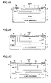
- FIG. 1 is a schematic surface view of a CCD color solid-state image pickup device of single plate type according to a first embodiment of the invention
- FIGS. 2A and 2B are descriptive views for reading signals from respective light-receiving sections of the CCD color solid-state image pickup device shown in FIG. 1 ;
- FIG. 3 is a descriptive view for reproducing colors from color signals read from the CCD color solid-state image pickup device shown in FIG. 1 by two reading operations;
- FIG. 4A is a cross-sectional view taken along line a-a shown in FIG. 2A ;
- FIG. 6 is a view made by superimposing transfer electrodes on the pixels shown in FIG. 5 ;
- FIG. 8C is a view showing a relationship between a distance over which light has entered and traveled through a magenta filter Mg in a silicon substrate and a storage layer of the first embodiment;
- FIG. 9A is a view showing a spectral sensitivity spectrum of a B signal and that of a G signal, both signals being produced by a light-receiving section with the cyan filter Cy stacked thereon;
- FIG. 9B is a view showing a spectral sensitivity spectrum of the G signal and that of an R signal, both signals being produced by a light-receiving section with the yellow filter Ye stacked thereon;
- FIG. 14A is a cross-sectional view taken along line a-a shown in FIG. 13 ;
- FIG. 15A is a view showing a relationship between a distance over which light has entered and traveled through a cyan filter Cy in a silicon substrate and a storage layer of the second embodiment;
- FIG. 15B is a view showing a relationship between a distance over which light has entered traveled through a yellow filter Ye in a silicon substrate and a storage layer of the second embodiment;
- FIG. 16 is a schematic surface view of a CCD color solid-state image pickup device of single plate type according to a third embodiment of the invention.
- FIG. 17 is a descriptive view for reproducing colors from color signals read from the CCD color solid-state image pickup device shown in FIG. 16 by two reading operations;
- FIG. 18 is a plan view showing a pattern of element isolation regions corresponding to two horizontally-adjacent light-receiving sections (two pixels) of the CCD color solid-state image pickup device shown in FIG. 16 ;
- FIG. 19 is a plan view showing four light-receiving sections (four pixels) of the CCD color solid-state image pickup device shown in FIG. 16 ;
- FIG. 20A is a cross-sectional view taken along line a-a shown in FIG. 19 ;
- FIG. 20B is a cross-sectional view take along line b-b shown in FIG. 19 ;
- FIG. 21A is a view showing a relationship between a distance over which light has entered and traveled through a magenta filter Mg in a silicon substrate and a storage layer of the third embodiment;
- FIG. 21B is a view showing a relationship between a distance over which light has entered and traveled through a green filter G in a silicon substrate and a storage layer of the third embodiment
- FIG. 22 is a view showing a spectral sensitivity spectra of the primary color signals produced by the color solid-state image pickup device of the third embodiment of the invention.
- FIG. 23 is a schematic surface view of a CCD color solid-state image pickup device of single plate type according to a fourth embodiment of the invention.
- FIG. 24 is a descriptive view for reproducing colors from color signals read from the CCD color solid-state image pickup device shown in FIG. 23 by two reading operations;
- FIG. 25 is a plan view showing four light-receiving sections (four pixels) of the CCD color solid-state image pickup device shown in FIG. 23 ;
- FIG. 26A is a cross-sectional view taken along line a-a shown in FIG. 25 ;
- FIG. 26B is a cross-sectional view take along line b-b shown in FIG. 25 ;
- FIG. 27B is a view showing a relationship between a distance over which light has entered and traveled through a white filter W in a silicon substrate and a storage layer of the fourth embodiment
- FIG. 28 is a view showing a spectral sensitivity spectra of the primary color signals produced by the color solid-state image pickup device of the fourth embodiment
- FIG. 29 is a schematic surface view of a CCD color solid-state image pickup device of single plate type according to a fifth embodiment of the invention
- FIG. 30 is a schematic surface view of a CMOS color solid-state image pickup of single plate type according to a sixth embodiment of the invention
- FIG. 31B is a cross-sectional view take along line XXXIb-XXXIb shown in FIG. 30 ;
- FIG. 32B is a cross-sectional view take along line XXXIIb-XXXIIb shown in FIG. 30 ;
- FIG. 33 is an equivalent circuit diagram of amplifiers shown in FIGS. 31A , 31 B, 32 A, and 32 B [i.e., amplifier circuits (source follower amplifiers)];
- FIG. 34B is a graph showing the potential profile of a light-receiving section with a Mg filter stacked thereon shown in FIG. 30 ;
- FIG. 35B is a graph showing the potential profile of a light-receiving section with a G filter stacked thereon shown in FIG. 30 ;
- FIG. 36A is a graph showing a spectral characteristic of the light-receiving section with a Cy filter stacked thereon shown in FIG. 30 ;
- FIG. 36B is a graph showing a spectral characteristic of the light-receiving section with a Mg filter stacked thereon shown in FIG. 30 ;
- FIG. 37A is a graph showing a spectral characteristic of the light-receiving section with a Ye filter stacked thereon shown in FIG. 30 ;
- FIG. 40B is a cross-sectional view of the CMOS color solid-state image pickup shown in FIG. 31B on which a microlens, a light-shielding film, or the like are stacked;
- FIG. 41A is a cross-sectional view of the CMOS color solid-state image pickup shown in FIG. 32A on which a microlens, a light-shielding film, or the like are stacked;
- FIG. 41B is a cross-sectional view of the CMOS color solid-state image pickup shown in FIG. 32B on which a microlens, a light-shielding film, or the like are stacked;
- FIG. 42 is a schematic surface view of a CMOS color solid-state image pickup of single plate type according to a seventh embodiment of the invention.
- FIG. 44 is a two-dimensional plan view corresponding to four pixels of the light-receiving sections with Cy, Ye filters stacked thereon of the color solid-state image pickup device shown in FIG. 42 ;
- FIG. 50 is a descriptive view reproducing color information by means of obtaining three color signals R, G, and B at the positions of the light-receiving sections with the filters (Mg, W) stacked thereon shown in FIG. 49 ;
- FIG. 51 is a cross-sectional schematic view taken along line LI-LI shown in FIG. 49 ;
- FIG. 52 is a cross-sectional view of the CMOS color solid-state image pickup shown in FIG. 51 on which a microlens, a light-shielding film, or the like are stacked;
- FIG. 53 is a view showing the potential profile of the light-receiving section on which a W filter shown in FIG. 49 is stacked;
- FIG. 54 is a graph showing a spectral characteristic of the CMOS color solid-state image pickup device shown in FIG. 49 ;
- FIG. 55 is a descriptive view of a related-art color solid-state image pickup device.
- FIGS. 56A to 56C are descriptive views of a related-art color solid-state image pickup device.
- FIG. 1 is a schematic surface view of a CCD color solid-state image pickup of single plate type according to a first embodiment of the invention.
- a plurality of light-receiving sections 1 are formed in an array on the surface of a semiconductor substrate 10 .
- each light-receiving section 1 is depicted as a rhombus.
- the arrangement of pixels employed in the present embodiment corresponds to the arrangement of pixels described in JP-A-10-136391; that is, a so-called honeycomb pixel arrangement in which the respective light-receiving sections 1 are offset at half a pitch in both the vertical and horizontal directions.
- a vertical transfer path e.g., a vertical charge-coupled device (VCCD)] 2 (signal reading unit) is formed between adjacent light-receiving sections 1 , and signal electric charges read to the vertical transfer path 2 from the respective light-receiving sections 1 are transferred, in a meandering manner, to a horizontal transfer path [e.g., a horizontal charge-coupled device (HCCD) ] 3 located at a lower position on the drawing.
- VCCD vertical charge-coupled device
- any of a yellow (Ye) filter, a cyan (Cy) filter, and a magenta (Mg) filter are stacked on surfaces of the respective light-receiving sections 1 .
- the Ye filter permits passage of light having green (G) and red (R) wavelength components;
- the Cy filter permits passage of light having blue (B) and the green (G) wavelength components;
- the Mg filter permits passage of light having the red (R) and blue (B) wavelength components.
- Each light-receiving section 1 of the embodiment has a cross-sectional structure which will be described in detail later. Therefore, the light-receiving section 1 can simultaneously store, from G+R light having passed through the Ye filter, a signal electric charge corresponding to the quantity of G and a signal electric charge corresponding to the quantity of Rand separately read the thus-stored signal electric charges to the vertical transfer path 2 .
- the light-receiving section 1 can simultaneously store, from B+G light having passed through the Cy filter, a signal electric charge corresponding to the quantity of B and a signal electric charge corresponding to the quantity of G and separately read the thus-stored signal electric charges to the vertical transfer path 2 .
- the light-receiving section 1 can simultaneously store, from R+B light having passed through the Mg filter, a signal electric charge corresponding to the quantity of R and a signal electric charge corresponding to the quantity of B and separately read the thus-stored signal electric charges to the vertical transfer path 2 .
- reading of a G signal from the light-receiving section 1 having the Ye filter, reading of a B signal from the light-receiving section having the Cy filter, and reading of an R signal from the light-receiving section having the Mg filter are performed by a first reading operation.
- reading of an R signal from the light-receiving section 1 having the Ye filter, reading of a G signal from the light-receiving section having the Cy filter, and reading of a B signal from the light-receiving section having the Mg filter are performed by a second reading operation.
- reading of signal electric charges from the light-receiving sections, transfer of the signal electric charges through the VCCD, and transfer of the signal electric charges through the HCCD are performed twice over the entire light-receiving area, whereby two primary-color signal components can be obtained from one light-receiving section.
- a deficient one-color signal in each light-receiving section is determined as a mean value of signals from surrounding pixels.
- the B signal read by the first reading operation and the G signal read by the second reading operation are used for reproducing a color of the location enclosed by a circle.
- a mean value of a total of six R signals (R signals from surrounding three pixels ⁇ 2) is used for determining a deficient R signal.
- a color of the position enclosed by the circle is reproduced by means of the thus-determined R, G, and B signals pertaining to the position enclosed by the circle.
- FIG. 4A is a cross-sectional view taken along line a-a shown in FIG. 2 ;
- FIG. 4B is a cross-sectional view taken along line b-b shown in FIG. 2 ;
- FIG. 4C is a cross-sectional view taken along line c-c shown in FIG. 2 .
- a complementary filter and a microlens provided thereon are omitted from the drawings.
- the CCD color solid-state image pickup device of the present embodiment separates the R, G, and B color signal components by utilization of an optical characteristic of the silicon substrate.
- the light absorption coefficient of a silicon substrate changes across a visible range from light of long wavelength (R) to light of short wavelength (B).
- R long wavelength
- B short wavelength
- light in a wavelength range having a large light absorption coefficient is absorbed by a shallow area of the silicon substrate, and hence the light hardly reaches a deep area of the silicon substrate.
- light in a wavelength range having a small light absorption coefficient reaches a deep region of the silicon substrate. Therefore, the light can be subjected to photoelectric conversion even at the deep area of the silicon substrate.
- a light-receiving section on which the cyan (Cy) filter is stacked and which stores blue (B) and green (G) signal electric charges, is formed in an n-type semiconductor substrate 10 .
- a P-well layer 11 is formed on the surface of the semiconductor substrate 10 , and two N + layers 12 , 13 (color signal detecting layers) are formed within the P well layer 11 so as to be separated from each other in the depthwise direction.
- the signal electric charges primarily produced from an incident light component of short wavelength light are stored in the N + layer 12 provided at the most shallow position with respect to the depthwise direction of the semiconductor substrate 10 .
- the N + layer 12 constituting the signal electric charge storage section extends up to a position below a read gate electrode 6 a ⁇ dopant [phosphorous or arsenic (P or As)] content is about 5 ⁇ 10 16-17 /cm 3 , and the depth of the N + layer is 0.2 to 0.4 ⁇ m, wherein the depth is dependent on the dopant content, and the same also applies to any counterparts in the following descriptions ⁇ . Therefore, only the electric charges derived primarily from the light of short wavelength pass through a gate section and are read to the vertical transfer path 2 .
- the N + layer (n 2 ) 13 provided at a position slightly deeper than the N + layer 12 has, at an end section thereof, an N + region (i.e., a charge path) 13 a which extends up to the surface of the semiconductor substrate 10 .
- This charge path 13 a extends up to a position below a read gate electrode 7 a formed from a portion of the transfer electrode.
- the signal electric charges formed from light of intermediate wavelength (e.g., G) are stored in the N + layer 13 .
- the N + layer 13 constituting the signal electric charge storage section (dopant content is about 5 ⁇ 10 16-17 /cm 3 at a depth of 0.4 to 0.8 ⁇ m) extends up to a position below the read gate electrode 7 a .
- the electric charges derived primarily from the light of intermediate wavelength (G) pass through a gate section and are read to the vertical transfer path 2 .
- a light-receiving section on which the yellow (Ye) filter is stacked and which stores green (G) and red (R) signal electric charges, is formed within the P well layer 11 as two N + layers 13 ′, 14 (color signal detecting layers) which are separated from each other in a depthwise direction.
- N + layer (n 2 ′) 13 ′ extends to a position below the read gate electrode 7 a constituting a portion of the transfer electrode.
- the signal electric charges formed from light of intermediate wavelength (e.g., G) are stored in the N + layer 13 ′.
- the N + layer 13 ′ constituting the signal electric charge storage section (dopant content is about 5 ⁇ 10 16-17 /cm 3 at a depth of 0.2 to 0.8 ⁇ m) extends up to a position below the read gate electrode 7 a .
- the electric charges derived primarily from the light of intermediate wavelength (G) pass through a gate section and are read to the vertical transfer path 2 .
- the structure of the N + layer 13 shown in FIG. 4A may be adopted in lieu of the N + layer 13 ′. Even if the electric charge storage layer 13 ′ is formed as an N + layer up to a depth of 0.8 ⁇ m or the like from the surface as in the case of the embodiment, the yellow (Ye) filter is stacked on the surface of the electric charge layer. Of the incident light, B light is blocked by the yellow filter, and hence B signal electric charges are not stored in the electric charge storage layer 13 ′.
- the N + layer (n 3 ) 14 formed at a deep position has, at an end section thereof, an N + region (i.e., a charge path) 14 a which extends up to the surface of the semiconductor substrate 10 .
- This N + region 14 a extends up to a position below the read gate electrode 6 a formed from a portion of the transfer electrode.
- the signal electric charges formed from light of long wavelength (e.g., R) are stored in the N + layer 14 .
- the N + layer 14 constituting the signal electric charge storage section (dopant content is about 5 ⁇ 10 16-17 /cm 3 at a depth of 0.8 to 2.5 ⁇ m) extends up to a position below the read gate electrode 6 a .
- the electric charges derived primarily from the light of long wavelength (R) pass through the gate section and are read to the vertical transfer path 2 .
- a light-receiving section on which the magenta (Mg) filter is stacked and which stores blue (B) and red (R) signal electric charges, is formed within the P well layer 11 as two N + layers 12 , 14 (color signal detecting layers) which are separated from each other in a depthwise direction.
- Mg magenta
- R red
- Signal electric charges derived primarily from an incident light component of short wavelength light (B) are stored in the N + layer 12 located at the surface and read to the vertical transfer path 2 by way of the gate section.
- Signal electric charges derived from light of long wavelength (e.g., R) are stored in the N + layer (n 3 ) 14 formed at a deep position and read to the vertical transfer path 2 by way of the gate section.
- a shallow P + layer 15 is provided in a portion of the surface of the semiconductor substrate 10 equipped with three types of storage sections 12 , 13 ( 13 ′), and 14 formed at different depths. Further, an SiO 2 film 16 is provided on the top surface of the semiconductor substrate 10 .
- a dopant (boron) content of the P + layer 15 is about 1 ⁇ 10 18 /cm 3 , and the P + layer 15 has a depth of about 0.1 to 0.2 ⁇ m. The dopant content contributes to a reduction in a defect level of an oxide film-semiconductor boundary surface. Accordingly, the storage section 12 located at the most shallow position in the depthwise direction of the semiconductor substrate 10 assumes a P + N + P structure.
- the CCD color solid-state image pickup device of the embodiment as a whole assumes a P + (N + P) (N + P) structure.
- Two types of storage sections (N + layers) of different depths are formed so as to be separated from each other with a P region (which will become a potential barrier) being sandwiched therebetween in the depthwise direction of the substrate.
- the boron content of the P region located between the N + layers is set to 1 ⁇ 10 14-16 /cm 3 .
- the dopant content of the storage section formed from the N + layers and that of the electric charge path are preferably given a concentration gradient so as to become higher toward the read gate section than at the light incidence region close to the center of the storage-section.
- reading of the signal electric charges becomes easy, and retention of unread electric charges can be prevented.
- double-layer storage sections are formed in any of the light-receiving sections 1 in the depthwise direction of the substrate, and there is provided no N + layer assigned to light of wavelength which is beyond the range of wavelengths for which signal electric charges are stored.
- a complementary color filter is stacked on each light-receiving section 1 , and hence one of the R, G, and B color signals is blocked by the complementary color filter, to thereby fail to reach the silicon substrate.
- FIG. 5 is a plan view showing a pattern of four pixels of the light-receiving section 1 shown in FIG. 1 and a pattern of the vertical transfer path 2 laid between the light-receiving sections 1 .
- the light-receiving sections 1 are partitioned from each other by means of rhombus element isolation regions 4 .
- gate sections 4 a , 4 b are formed in two right sides where the element isolation region 4 is broken.
- signal electric charges stored in the respective storage sections 12 , 13 , and 14
- signal electric charges (see FIG. 2A ) which are to be read by the first reading operation are read to the vertical transfer path 2 by way of the gate section 4 a .
- the signal electric charges (see FIG. 2B ) which are to be read by the second reading operation are read to the vertical transfer path 2 by way of the gate section 4 b.
- FIG. 6 is a view made by superimposing transfer electrodes on the pixels shown in FIG. 5
- FIG. 7 is a detailed view of the inside of an area enclosed by a circle VII shown in FIG. 6
- the transfer electrode formed from a two-layer polysilicon structure is provided so as to cover the vertical transfer path 2 .
- Four transfer electrodes 5 , 6 , 7 , and 8 are assigned to one light-receiving section 1 .
- the electrodes constitute a so-called CCD which can read all pixels (i.e., a CCD capable of performing progressive operation).
- FIGS. 8A , 8 B, and 8 C are conceptual renderings for describing the fact that depths of the silicon substrate to which the light signals having passed through the complementary color filters Cy, Ye, and Mg travel change according to wavelengths of the light signals.
- the B light having the shortest wavelength
- the G light having an intermediate wavelength
- n 2 (n 2 ′) located at the intermediate depth
- electric charges produced by the R light are stored in a storage region n 3 located at the deepest location of the silicon substrate.
- a P region which is to act as a potential barrier, exists between the signal charge storage sections n 1 , n 2 and between the signal charge storage sections n 2 (n 2 ′), n 3 .
- Signal charges (i.e., electrons) having developed in the P region are allocated to any of the adjacent charge storage sections [n 1 , n 2 (n 2 ′), n 3 ] along a potential profile.
- FIG. 9A is a view showing a spectral sensitivity spectrum of the B signal and that of the G signal, both signals being produced by the light-receiving section with the cyan (Cy) filter stacked thereon.
- FIG. 9B is a view showing a spectral sensitivity spectrum of the G signal and that of the R signal, both signals being produced by the light-receiving section with the yellow (Ye) filter stacked thereon.
- FIG. 9C is a view showing a spectral sensitivity spectrum of the B signal and that of the R signal, both signals being produced by the light-receiving section with the magenta (Mg) filter stacked thereon.
- Mg magenta
- the CCD color solid-state image pickup device of the embodiment increases the utilization efficiency of incident light through use of complementary color filters, thereby enhancing sensitivity. Moreover, the respective light-receiving sections can distinguish color signals and directly read primary color signals, thereby obviating a necessity for color signal separation computation processing.
- FIG. 10 is a schematic surface view of a CCD color solid-state image pickup device of single plate type according to a second embodiment of the invention.
- the dopant content of the N + layer or the like and the depth of the storage layer are the same as those described in connection with the first embodiment.
- the G signal read through the first reading operation and the R signal read through the second reading operation are used for reproducing a color of the area enclosed by, e.g., a circle.
- a mean value of B signals of four peripheral signals from the adjacent pixels is used as a deficient B signal.
- FIG. 13 is a view showing a transfer electrode of a color solid-state image pickup device of the embodiment.
- transfer electrodes 25 , 26 , and 27 have a triple-layer polysilicon structure and are constituted of interline CCDs which can read all pixels.
- the second polysilicon electrode 26 and the third polysilicon electrode 27 constitute read gate electrodes. When a read voltage is applied to the respective read gate electrodes, a signal electric charge is read to the vertical transfer path 22 from the corresponding signal electric charge storage section.
- a P well layer 31 is formed on the surface of an n-type semiconductor substrate 30 of the color solid-state image pickup device of the embodiment.
- Signal electric charge storage layers 32 , 33 are formed from a two-layer N + structure within the P well layer 31 so as to be separated from each other in a depthwise direction.
- a storage layer (n 1 ) 32 provided in a surface section extends up to a position below the read gate electrode 26 a formed from a portion of the transfer electrode.
- the signal electric charges primarily produced from an incident light component of short wavelength (e.g., B) are stored in the storage layer 32 provided at the most shallow position with respect to the depthwise direction of the semiconductor substrate 30 .
- the electric charges stored in the storage layer 32 that is, the electric charges produced primarily from light of short wavelength, are read to the vertical transfer path 22 .
- the second storage layer (n 2 ) 33 has, at an end section thereof, an N + region (i.e., a charge path) 33 a which extends up to the surface of the semiconductor substrate 30 .
- This N + region 33 a extends up to a position below a read gate electrode 27 a formed from a portion of the transfer electrode.
- the signal electric charges formed from light of intermediate wavelength (e.g., G) are stored in the this storage layer 33 .
- the electric charges stored in the storage layer 33 that is, the electric charges produced primarily from the light of intermediate wavelength (G), are read to the vertical transfer path 22 .
- a light-shielding film 40 having openings to oppose a light-receiving surface of the light-receiving section is placed on top of the light-receiving section in which the storage layers 32 , 33 of such a configuration are formed.
- a Cy filter 41 and a microlens 42 are stacked on the light-shielding film 40 . Light is gathered by the microlens 42 , and the incident light—for which light of a red (R) wavelength is blocked by the Cy filter— 41 enters the light-receiving section by way of an opening 40 a of the light-shielding film 40 .
- the P + layer 15 and the SiO 2 film 16 are provided on the top surface of the semiconductor substrate 30 .
- signal electric charge storage layers 34 , 35 are formed from an N + layer of two-layer structure within the P well layer 31 , which is formed on the surface of the n-type semiconductor substrate 30 , so as to be separated from each other in the depthwise direction.
- the storage layer (n 2 ′) 34 of the surface section is formed up to about the same depth as that of the storage layer 33 shown in FIG. 14A .
- the end section of the storage layer 34 extends up to a position below the read gate electrode 26 a formed from a portion of the transfer electrode 26 .
- the signal electric charges primarily produced from an incident light component of intermediate wavelength e.g., G
- G an incident light component of intermediate wavelength
- the storage layer (n 3 ) 35 formed at a deep position of the P well layer 31 has, at an end section thereof, an N + region (i.e., a charge path) 35 a which extends up to the surface of the semiconductor substrate 30 .
- This N + region 35 a extends up to a position below the read gate electrode 27 a formed from a portion of the transfer electrode 27 .
- the signal electric charges formed from light of long wavelength (e.g., R) are stored in the this storage layer 35 . In this structure, only the electric charges stored in the storage layer 35 are read to the vertical transfer path 22 .
- An opening 40 b of the light-shielding film 40 is also placed also on the light-receiving section in which the storage layers 34 , 35 of such a configuration are formed.
- a Ye filter 43 and a microlens 44 are stacked on the opening 40 b .
- Light is gathered by the microlens 44 , and the incident light—for which light of a blue (B) wavelength is blocked by the Ye filter 43 —enters the light-receiving section by way of the opening 40 b of the light-shielding film 40 .
- a P + layer 15 and a SiO 2 film 16 are formed on the top surface of the semiconductor substrate 30 .
- the storage layer 34 of the embodiment is distributed up to the surface of the substrate. However, light corresponding to B light of short wavelength is blocked by the Ye filter. Hence, the storage layer 34 has no sensitivity against incident B light. Therefore, no particular restrictions are imposed on the distribution of the storage layer 34 in a depth direction.
- the storage layer 34 may be formed in the same structure as that of the storage layer 33 shown in FIG. 14A (i.e., a structure in which the storage layer is not distributed up to the neighborhood of the surface of the semiconductor substrate).
- FIGS. 15A and 15B are conceptual renderings for the phenomenon that, in the solid-state image pickup device of the embodiment, distances over which the light signals having passed through the Cy filter 41 and the Ye filter 43 travel in the depthwise direction of the silicon substrate change according to wavelengths of the light signals.
- blue (B) light having the shortest wavelength is absorbed in the most shallow region of the silicon substrate, whereby electric charges corresponding to the quantity of B light are generated and then stored in the first storage layer n 1 .
- the green (G) light of an intermediate wavelength reaches a position deeper than that at which the blue (B) light arrives, and hence large portions of produced electric charges are stored in the storage layer n 2 .
- green (G) light of intermediate wavelength is stored in the storage layer n 2 ′.
- electric charges produced from the R light of longest wavelength are stored in the storage layer n 3 located at the deepest location of the silicon substrate.
- the embodiment has described a solid-state image pickup device having the light-receiving sections 21 arranged in a square grid pattern.
- the embodiment can be readily applied to a solid-state image pickup device having the light-receiving sections 21 arranged in a so-called honeycomb pattern.
- FIG. 16 is a schematic surface view of a CCD color solid-state image pickup device of single plate type according to a third embodiment of the invention.
- a light-receiving section 51 is represented by a rectangle, and a plurality of light-receiving sections 51 are arranged in an array.
- the light-receiving sections 51 are arranged in a square grid pattern.
- a vertical transfer path 52 (signal reading unit) is formed between horizontally-adjacent light-receiving sections 51 . Signal electric charges read from the light-receiving section 51 to the vertical transfer path 52 are transferred to a horizontally transfer path 53 placed at a downward position.
- B and R signals are output from the light-receiving section 51 with the Mg filter stacked thereon. Therefore, the primary color signal component of one color (G) is output from the light-receiving sections 51 having the G filter by twice performing operations for receiving electric charges from the light-receiving sections and transferring the thus-read electric charges to the VCCD and HCCD. Further, two primary color signal components of two colors (R, B) are output from the light-receiving section having the Mg filter.
- G only one color (G) component is output from the light-receiving section 51 with the G filter stacked thereon.
- G signals (a first signal is G 1 , and a second signal is G 2 ) read through two reading operations are used at this light-receiving position while being added together.
- a remaining R color is obtained by averaging peripheral R signals, and a remaining B color is obtained by averaging peripheral B signals.
- two colors are obtained from the light-receiving sections with the Mg filter stacked thereon.
- Four peripheral G 1 signals and four peripheral G 2 signals are used for determining the remaining G signal.
- FIG. 18 is a plan view showing two pixels of the light-receiving section 51 and the vertical transfer path laid between the horizontally-adjacent light-receiving sections, both pertaining to the present embodiment.
- Each light-receiving section is surrounded by a C-shaped element isolation region 54 .
- Signal electric charges are read to the vertical transfer path 52 from a gate section 54 a where the element isolation region 54 is not present.
- FIG. 19 is a view showing a transfer electrode of a color solid-state image pickup device of the embodiment.
- transfer electrodes 55 , 56 , and 57 have a triple-layer polysilicon structure and constitute interline CCDs which can read all pixels.
- the second polysilicon electrode 56 and the third polysilicon electrode 57 constitute read gate electrodes. When a read voltage is applied to the respective read gate electrodes, a signal electric charge is read to the vertical transfer path 52 from the corresponding signal electric charge storage section.
- FIG. 20A is a cross-sectional view taken along line a-a shown in FIG. 19 ; that is, a cross-sectional view of a light-receiving section with the Mg filter stacked thereon; and
- FIG. 20B is a cross-sectional view taken along line b-b shown in FIG. 19 ; that is, a cross-sectional view of a light-receiving section with a G filter stacked thereon.
- a P well layer 61 is formed on the surface of an n-type semiconductor substrate 60 of the color solid-state image pickup device of the embodiment.
- Signal electric charge storage layers 62 , 63 are formed from a two-layer N + structure within the P well layer 61 so as to be separated from each other in a depthwise direction.
- the P + layer 15 and the SiO 2 film 16 are provided on the top surface of the semiconductor substrate 60 .
- the color solid-state image pickup device of the embodiment has one or two storage layers in the depthwise direction of the substrate.
- the storage layers n 1 ( 62 ), n 2 ( 64 ), and n 3 ( 63 ) are arranged in the sequence of increasing sequence. Depths of the storage layers are set in the sequence of increasing depth such that B light signal electric charges, G light signal electric charges, and R light signal electric charges are stored.
- the electric charges of the respective storage layers can be read to the vertical transfer path independently. Specifically, single ends of the respective storage layers located in the N + region extend up to the neighborhood of different read gate sections.
- the electric charges stored in the storage layers can be read to the vertical transfer path by application of a read pulse ( ⁇ v).
- the G signal is read from the same storage layer 64 through two reading operations. However, all the stored electric charges may be read from the storage layer 64 by the first reading operation.
- FIG. 22 is a plot showing that a spectral sensitivity spectrum of the G signal output from the light-receiving section having the green filter stacked thereof is superimposed on spectral sensitivity spectra of the B and R signals output from the light-receiving sections having the magenta filter of the embodiment stacked thereon.
- the filter of complementary color system of the embodiment is only magenta, there is no necessity for superimposing cyan and yellow filters one on top of the other in order to implement a green filter. Only one green filter of primary color system can be provided. Further, the magenta filter permits passage of the B and R signals whose wavelengths are separated from each other. Hence, as shown in FIG. 22 , the spectral sensitivity spectra of the R, G, and B signals obtained in the embodiment become close to the ideal spectral sensitivity spectra which involves a smaller overlap and effects superior color separation. Therefore, color reproduction more faithful than that achieved in the first and second embodiments can be realized by means of subjecting the color signals produced by the solid-state image pickup device of the embodiment to image processing.
- each light-receiving section can directly read the primary color signal by means of making a distinction between color signals.
- a necessity for color signal separation processing operation is obviates, thereby enabling faithful reproduction of colors and rendering image quality high.
- the present embodiment has described the solid-state image pickup device having the light-receiving sections 21 arranged in a square grid pattern, the present embodiment can also be applied to a solid-state image pickup having the light-receiving sections 21 arranged in a so-called honeycomb pattern.
- FIG. 23 is a schematic surface view of a CCD color solid-state image pickup device of single plate type according to a fourth embodiment of the invention.
- this CCD color solid-state image pickup device a plurality of light-receiving sections 71 are formed in the form of an array on the surface of a semiconductor substrate 80 .
- each light-receiving section 71 is represented by a rhombus.
- the arrangement of pixels of the present embodiment is identical with that described in connection with the first embodiment; that is, a so-called honeycomb pixel arrangement formed by offsetting the light-receiving sections 71 by half pitches in both the vertical and horizontal directions.
- a vertical transfer path 72 (signal reading unit) is formed between adjacent light-receiving sections 71 , and signal electric charges read from the respective light-receiving sections 71 to the vertical transfer path 72 are transferred in a meandering manner to a horizontal transfer path 73 located at a downward position.
- Mg filters are stacked on the respective light-receiving sections 71 provided in even columns, and instead of the color filters, mere transparent planarized films (also called “white filters”) are stacked on the respective light-receiving sections 71 provided in odd columns.
- R signal electric charges formed from incident light components R which are not blocked by the Mg filter and B signal electric charges formed from incident light components B which are not blocked by the Mg filter are stored in a distinguished manner in the light-receiving sections 71 with the Mg filter stacked thereon.
- the R, B signal electric charges are read independently, and the light-receiving sections 71 having the W filter stacked thereon have sensitivity to all visible rays.
- the light-receiving sections having the Mg filters output R and B signals, and signals output from the light-receiving sections having the W filters are formed by adding all the R, G, and B signal components.
- W 1 and W 2 signals output by two reading operations are added together and used as the W signals to be output from the light-receiving sections having the W filters.
- the light-receiving sections having the Mg filters stacked thereon output two primary color signal components R, B in such a manner as shown in FIG. 24 .
- the magnitude of the R signal and that of the B signal are subtracted from the two primary color signals R, B, and a mean value (R+G+B) of four or eight peripheral W signals, thereby determining the G signal as color information pertaining to the location of the light-receiving section having the Mg filter.
- the R signal is determined from a mean value of four peripheral R signals as color information pertaining the position of the light-receiving section having the W filter.
- the B signal is determined from a mean value of four peripheral B signals.
- the G signal is determined by subtracting the magnitude of the R signal and that of the B signal from the magnitude of the directly obtained W signal.
- FIG. 25 is a plan view showing a pattern of four pixels of the light-receiving section 71 shown in FIG. 23 and a pattern of the vertical transfer path 72 laid between the light-receiving sections 71 .
- the light-receiving sections 71 are partitioned from each other by means of rhombus element isolation regions 74 .
- gate sections 74 a , 74 b are formed in two right sides where the element isolation region 74 is broken.
- the first W signal is read from the light-receiving section 71 having the W filter, by way of the gate section 74 a .
- a second W signal is read by way of the gate section 74 b . All the W signals of the light-receiving section 71 may be read by one W signal reading operation.
- the transfer electrode structure provided on the vertical transfer path 72 is the same as that employed in the first embodiment; that is, two-layer polysilicon.
- FIG. 26A is a cross-sectional view of the light-receiving section having a W filter taken along line a-a shown in FIG. 25 .
- a P well layer 81 is formed on the surface of an n-type semiconductor substrate 80 .
- a signal electric charge storage layer (n 2 ) 82 (color signal detecting layer) which is as deep as 0.2 to 2.5 ⁇ m and formed from an N + layer is formed in the surface of the P well layer 81 .
- the P + layer 15 and the SiO 2 film 16 are provided on the top surface of the light receiving section.
- An opening 85 a of a light-shielding film 85 is provided on a light-receiving surface of the light-receiving section.
- a transparent planarized film 86 that is, a W filter, is provided on the opening 85 a .
- a microlens 87 is provided at a position above the planarized film 86 . The incident light gathered by the microlens 87 passes through the transparent planarized film 86 , thereby entering the storage layer 82 with a small loss.
- FIG. 26B is a cross-sectional view taken along line b-b shown in FIG. 25 ; that is, a cross-sectional view of a light-receiving section having a Mg filter.
- Signal electric charge storage layers 83 , 84 (color signal detecting layers), both being formed from an N + layer of two-layer structure, are formed separately in the P well layer 81 formed on the n-type semiconductor substrate 80 . As mentioned above, the P + layer 15 and the SiO 2 film 16 are formed on top of the light-receiving section.
- the storage layer (n 1 ) 83 provided at the surface section extends up to a position below the read gate electrode formed from a portion of the transfer electrode.
- Signal-electric charges formed primarily from incident light components of short wavelength light e.g., B
- the electric charges stored in the storage layer 83 are read to the vertical transfer path 72 .
- the storage layer (n 3 ) 84 formed at a deep location has, at an end section thereof, an N + region (i.e., a charge path) 84 a which extends up to the surface of the semiconductor substrate 80 .
- This N + region 84 a extends up to a position below the read gate electrode formed from a portion of the transfer electrode.
- the signal electric charges formed from light of long wavelength e.g., R
- the electric charges stored in the storage layer 84 that is, electric charges produced primarily from the light (R) of long wavelength, are read to the vertical transfer path 72 .
- An opening 85 b of a light-shielding film 85 is provided on the light-receiving section having the storage layers 83 , 84 of such a structure in alignment with the light-receiving surface of the light-receiving section. Moreover, a Mg filter 88 and a microlens 89 are stacked on the openings 85 b , and the microlens 89 gathers light. The incident light whose green (G) wavelength light is blocked by the Mg filter 88 enters the light-receiving section by way of the opening section 85 b of the light-shielding film 85 .
- G green
- the storage layer n 1 is the most shallow, and the storage layers n 2 , n 3 are located at essentially the same depth.
- the storage layer n 3 is localized at a spaced location so as not to contact the storage layer n 1 located above the storage layer n 3 .
- the storage layer n 3 is selectively set to a depth such that the highest sensitivity is achieved by the wavelength component of R light.
- the storage layer n 2 is distributed up to the neighborhood of the surface and to the same depth as that of the storage layer n 3 . The reason for this is that the incident light wavelength components in a visible range which can be perceived by the human eye are subjected to photoelectric conversion most efficiently and that the colorless (W) filter is stacked on the light-receiving section.
- FIGS. 27A and 27B are conceptual renderings for describing a difference in distances over which the light signals having passed through the Mg and W filters travel in the depthwise direction of the silicon substrate for reasons of their wavelengths.
- the B light which is of shortest wavelength, is absorbed by the most shallow region of the silicon substrate, thereby producing electric charges.
- the thus-produced electric charges are stored in the first storage layer n 1 .
- the electric charges produced by the R light which is of longest wavelength, are stored in the storage layer n 3 located at the deepest position in the silicon substrate.
- the light-receiving sections, each having the W filter 86 must subject all the R, G, and B light beams to photoelectric conversion.
- the storage layer n 2 is distributed widely from a shallow portion to a deep portion of the substrate.
- FIG. 28 is a view showing a spectral sensitivity spectrum of the color solid-state image pickup device of the embodiment.
- the B and R signals having passed through the magenta Mg filter are separated from each other without an overlap.
- the signal (W) of light (B+G+R) having passed through the W filter includes all visible light wavelength ranges and assumes a spectrum whose peak appears at the wavelength of the G signal (i.e., the neighborhood of a wavelength of 540 nm).
- the light-receiving sections assigned the white (W) filters can utilize wavelength components of all visible ranges, and hence no substantial loss arises in the incident light component.
- the complementary color filters are stacked on all the light-receiving sections as in the first case, an attempt can be made to enhance sensitivity to a much greater extent.
- the present embodiment is also characterized in that a high-sensitivity luminance signal (R+G+B) is obtained directly without involvement of any particularly complicate signal processing operation. Since only the Mg filter is used as a color filter, a process for stacking color filters becomes easy.
- the present embodiment has described a solid-state image pickup device having the respective light-receiving sections 71 arranged in a so-called honeycomb pattern.
- the present embodiment can also be applied to a solid-state image pickup device having the light-receiving sections 71 arranged in a square grid pattern.
- FIG. 29 is a schematic surface view of a CCD color solid-state image pickup device according to a fifth embodiment of the invention.
- the present embodiment differs from the second embodiment only in that a green (G) filter, a magenta (Mg) filter, a yellow (Ye) filter, and a cyan (Cy) filter are stacked on respective light-receiving sections 91 arranged on a semiconductor substrate 90 in a square grid pattern.
- Color signal electric charges read from the respective light-receiving sections 91 to a vertical transfer path 92 (signal reading unit) are transferred to a horizontal transfer path 93 .
- the cross-sectional structure of each light-receiving section 91 is the same as that of the light-receiving section on which the same color filter as that employed in the previous embodiment is stacked.
- the only difference of the solid-state image pickup device of the embodiment lies in color filters to be stacked on the respective light-receiving sections.
- signals of “n” (“n” is an integer of 1 or more) lines are formed from green (G), yellow (Ye), cyan (Cy), and magenta (Mg), and a signal of n+1 lines is formed from magenta (Mg), yellow (Ye), cyan (Cy), and green (G). These signals are repeated.
- FIG. 30 is a schematic surface view of a CMOS color solid-state image pickup device according to a sixth embodiment of the invention.
- This CMOS color solid-state image pickup device is fabricated on the surface of an n-type semiconductor substrate 110 and comprises a light-receiving area 111 ; a vertical scanning circuit 112 formed beside the light-receiving area 111 ; and a horizontal scanning circuit or the like (e.g., a signal amplifier circuit, an analog-to-digital conversion circuit, a synchronous signal generation circuit, or the like) 113 formed at a position close to the bottom side of the semiconductor substrate 110 .
- a horizontal scanning circuit or the like e.g., a signal amplifier circuit, an analog-to-digital conversion circuit, a synchronous signal generation circuit, or the like
- a plurality of light-receiving sections are arranged and formed in a two-dimensional array or a square grid pattern within the light-receiving area 111 , and mono color filters are stacked on top of the respective light-receiving sections.
- Color filters of a complementary color system that is, cyan (Cy), yellow (Ye), magenta (Mg), and green (G) color filters, are used as the color filters.
- the G filters and the Mg filters are alternately arranged in odd rows, and the Ye filter and the Cy filter are alternately arranged in even rows.
- This color filter arrangement is generally called a color difference sequential arrangement.
- the arrangement can also be embodied by combination of three color filters Ye, Cy, and Mg which do not include the G filters. The case of four color filters will now be described.
- FIG. 31A is a cross-sectional block diagram taken along ///line XXXIa-XXXIa shown in FIG. 30 , i.e., a cross-sectional block diagram of a light-receiving section with a Cy filter 151 stacked thereon; and FIG. 31B is a cross-sectional block diagram taken along line XXXIb-XXXIb shown in FIG. 30 , i.e., a cross-sectional block diagram of a light-receiving section with an Mg filter 152 stacked thereon. Similarly, FIG. 32A is a cross-sectional block diagram taken along line XXXIIa-XXXIIa shown in FIG.
- FIG. 30 i.e., a cross-sectional block diagram of a light-receiving section with a Ye filter 153 stacked thereon; and FIG. 32B is a cross-sectional block diagram taken along line XXXIIb-XXXIIb shown in FIG. 30 , i.e., a cross-sectional block diagram of a light-receiving section with a G filter 154 stacked thereon.
- the light-receiving section with the Cy (cyan) filter 151 stacked thereon blocks only a red (R) light component of the incident light, whereupon B (blue) and G (green) light components reach the light-receiving section.
- a P well layer 115 is formed on the surface of an n-type semiconductor substrate 110 , and an N + layer (n 1 ) 116 (color signal detecting layer) having a depth of 0.1 to 0.3 ⁇ m is formed in the surface within the P well layer 115 .
- N + layer (n 2 ) 117 (color signal detecting layer) having a depth of 0.3 to 0.8 ⁇ m is formed at a slightly deep position within the P well layer 115 so as to be separated from the N + layer 116 .
- An electric charge path 117 a extending up to the surface of the light-receiving section is provided at an end section of the N + layer 117 .
- dopant [phosphorous or arsenic (P or As)] content of the N + layers 116 , 117 , and. 117 a is set to about 5 ⁇ 10 16-17 /cm 3 .
- the depths of the N + layers 116 , 117 are also dependent on this dopant content.
- a P region which is to act as a potential barrier is interposed between the N + layers 116 , 117 .
- the P region is maintained at the same potential as that of the P well layer 115 .
- the dopant (boron) content (1 ⁇ 10 15-16 /cm 3 ) of the P region existing between the N + layers 116 , 117 may be set so as to differ from that (7 ⁇ 10 14-15 /cm 3 ) of the P well layer 115 .
- the N + layer 116 is connected to a B signal detection amplifier 122 by way of an ohmic contact 121 .
- the electric charge path 117 a of the N + layer 117 is connected to a G signal detection amplifier 124 by way of an ohmic contact 123 .
- the dopant content of contact portions of the N + layers 116 , 117 a is set to 1 ⁇ 10 19 /cm 3 or higher.
- a reset transistor is activated before photographing a color image.
- a predetermined amount of electric charges are stored in PN junction sections of the respective N + layers 116 , 117 .
- the electric charges stored in the PN junction section of the N + layer 116 are discharged by an amount corresponding to the photocarriers produced in correspondence to the quantity of B (blue) incident light of the incident light arrived at the light-receiving section.
- the electric charges stored in the PN junction section of the N + layer 117 are discharged by an amount corresponding to the photocarriers produced in correspondence to the quantity of G (green) incident light.
- the amount of changes in the electric charges stored in the respective PN junctions of the respective N + layers 116 , 117 are independently read by amplifiers 122 , 124 as B and C signals.
- the light-receiving section with the Mg (magenta) filter 152 stacked thereon blocks only a green (G) light component of the incident light, whereupon B (blue) and R (red) light components reach the light-receiving section.
- the N + layer (n 1 ) 116 that is the same as that described by reference to FIG. 31A is formed in the P well layer 115 formed in the surface of the n-type semiconductor substrate 110 .
- An N + layer (n 3 ) 118 (color signal detecting layer) having a depth of 0.8 to 2.5 ⁇ m is formed at a deeper position within the P well layer 115 so as to be separated from the N + layer 116 .
- An electric charge path 118 a extending up to the surface of the light-receiving section is provided at an end section of the N + layer 118 .
- the N + layer 116 is connected to the amplifier 122 by way of the ohmic contact 121 .
- the electric charge path 118 a is connected to an R signal detection amplifier 126 by way of an ohmic contact 125 .
- the dopant content of the P region located between the N + layers 116 , 118 may be set so as to differ from that of the P well layer 115 in the same manner as that described by reference to FIG. 31A .
- the dopant content of the N + layers 116 , 118 , and 118 a and the dopant content of the ohmic contact sections are the same as those described by reference to FIG. 31A .
- the dopant content also applies to the following descriptions.
- the reset transistor is activated before photographing a color image, whereby a predetermined amount of electric charges are stored in PN junction sections of the respective N + layers 116 , 118 .
- the electric charges stored in the PN junction section of the N + layer 116 are discharged by an amount corresponding to the photocarriers produced in correspondence to the quantity of B (blue) incident light of the incident light having arrived at the light-receiving section.
- the electric charges stored in the PN junction section of the N + layer 118 are discharged by an amount corresponding to the photocarriers produced in correspondence to the quantity of R (red) incident light.
- the amounts of changes in the electric charges are independently read by amplifiers 122 , 126 as B and R signals.
- the light-receiving section with the Ye (yellow) filter 153 stacked thereon blocks only the B (blue) light component of the incident light, whereupon the G (green) and R (red) light components arrive at the light-receiving section.
- the N + layer (n 3 ) 118 that is the same as that described by reference to FIG. 31B is formed within the P well layer 115 formed on the surface of the n-type semiconductor substrate 110 .
- An N + layer (n 2 ′) 119 (color signal detecting layer) having a depth of 0.1 to 0.8 ⁇ m is formed in the surface so as to be separated from the N + layer 118 .
- a G signal detection amplifier 128 is connected to the N + layer 119 by way of an ohmic contact 127 .
- the reset transistor is activated before photographing a color image, whereby a predetermined amount of electric charges are stored in PN junction sections of the respective N + layers 118 , 119 .
- the electric charges stored in the N + layer 119 are discharged by an amount corresponding to the photocarriers produced in correspondence to the quantity of G (green) incident light of the incident light having arrived at the light-receiving section.
- the electric charges stored in the N + layer 118 are discharged by an amount corresponding to the photocarriers produced in correspondence to the quantity of R (red) incident light. Changes in the amounts of electric charges of the respective N + layers 118 , 119 are independently read by amplifiers 126 , 128 as R and G signals.
- the N + layer 119 for detecting a G signal is set to a depth of 0.1 to 0.8 ⁇ m.
- the N + layer 119 may be formed to a depth ranging from 0.3 to 0.8 ⁇ m.
- B (blue) light of the incident light is blocked by the Ye filter.
- a change in the amount of electric charges corresponding to the amount of incident light G (green) arises in the N + layer 119 , and hence mixing of B and G colors does not arise.
- the light-receiving section with the G (green) filter 154 stacked thereon permits transmission of only the G (green) light component of the incident light, thereby blocking the B (blue) and R (red) light components from arriving at the light-receiving section.
- the N + layer (n 2 ′) 119 having the same depth as that described by reference to FIG. 32A ; that is, a depth of 0.1 to 0.8 ⁇ m, is formed in the surface of the P well layer 115 formed on the n-type semiconductor substrate 110 .
- the amplifier 128 for detecting a G signal is connected to the N + layer 119 by means of the ohmic contact 127 .
- the reset transistor is activated before photographing a color image, whereupon a predetermined amount of electric charges are stored in the PN junctions of the respective N + layers 119 .
- the thus-stored electric charges are discharged by an amount corresponding to the photocarriers produced in correspondence to the quantity of G (green) incident light of the incident light having passed through the G filter.
- a signal corresponding to the amount of change in electric charges is read as a G signal by the amplifier 128 .
- the G filter may be formed as a primary color filter.
- the G filter may be imparted with a filtering characteristic of permitting transmission of only G light superimposing the yellow filter and the cyan filter, both being filters of a complementary color system, one on top of the other.
- the configurations of the amplifiers 122 , 124 , 126 , and 128 include the equivalent circuits shown in FIG. 33 . Although omitted from FIGS. 31 and 32 , the topmost surface of the semiconductor substrate other than those occupied by the contact sections is covered with a protective SiO 2 film.
- FIGS. 34A , 34 B and FIGS. 35A , 35 B are views showing the relationship between the potential profile of the light-receiving sections of the color solid-state image pickup device of the embodiment—the Cy filter, the Mg filter, the Ye filter, and the G filter are stacked on the light-receiving sections—in the depthwise direction of the substrate and the depth to which incident light enters.
- the light-receiving section of the embodiment with the filters of a complementary color system stacked thereon is characterized by comprising two-stages; that is, an N + region and a P region interposed between the N + regions, in the depthwise direction of the substrate.
- the depths of the respective N + regions (n 1 , n 2 , and n 3 ) change dependent on the stacked filters of a complementary color system.
- signals of incident light wavelengths which have not been blocked by the filters of a complementary color system and subjected to photoelectric conversion must be read independently.
- the depths of the impurity layers are determined such that the incident light is subjected to photoelectric conversion most efficiently, whereby a read circuit is connected.
- the B light having the shortest wavelength is absorbed by the most shallow area of the silicon substrate.
- photocarriers are produced in the vicinity of the n 1 layer (N + layer 116 ).
- the G light formed from an intermediate wavelength reaches a position deeper than that achieved by the B light.
- photocarriers are induced in the vicinity of the n 2 layer (N + layer 117 ) located at an intermediate depth.
- photocarriers are produced by the R light having the shortest wavelength in the vicinity of the n 3 layer (N + layer 118 ) located at the deepest location of the silicon substrate.
- the B light is blocked by the G filter or the Ye filter.
- the N layer there is no necessity for dividing the N layer into the n 1 layer and the n 2 layer.
- the n 1 layer, the n 2 layer (n 2 ′ layer), and the n 3 layer are set in an increasing sequence of depth.
- the depths of the respective N + layers are set for such that the photoelectric conversion efficiency of the B light, that of the G light, and that of the R light become highest.
- FIGS. 36A , 36 B and FIGS. 37A , 37 B are views showing spectral sensitivity spectra of signals obtained by the light-receiving sections with the Cy filter, the Mg filter, the Ye filter, and the G filter stacked thereon.
- the horizontal axis shows the wavelength of incident light (nm), and the vertical axis shows relative sensitivity (%) of the output signal.
- each light-receiving section the wavelength dependence of the output signal is dominated by the spectral transmission factor of the stacked color filter.
- the filter of a complementary color system is stacked on the light-receiving section, there exists a P region, which is to act as a potential barrier existing between the N + layers; that is, a P region sandwiched between the N + layers.
- Signal charges (i.e., electrons) having developed in the P region are allocated to any of the adjacent N + layers by means of the potential barrier, thereby yielding an advantage of a small overlap existing between spectra.
- the color solid-state image pickup device of the embodiment yields an advantage of an increase in the performance for separating color signals attributable to use of only signals output from only the two N + layers.
- the majority of light of a wavelength corresponding to R is blocked by the Cy filter.
- the wavelength dependence of a signal output from the light-receiving section is sharply attenuated in this wavelength range. Accordingly, the B output signal and the G output signal are understood to be unaffected by the light of the R wavelength.
- the majority of light of a wavelength corresponding to G is blocked by the Mg filter.
- the wavelength dependence of a signal output from the light-receiving section is sharply attenuated in this wavelength range. Accordingly, the B output signal and the R output signal exhibit spectra having no essential overlaps therebetween.
- the majority of light of a wavelength corresponding to B is blocked by the Ye filter.
- the wavelength dependence of a signal output from the light-receiving section is sharply attenuated in this wavelength range. Accordingly, the G output signal and the R output signal are understood to be unaffected by the light of the B wavelength.
- the G filter In the light-receiving section with the green (G) filter stacked thereon, the majority of light of wavelengths corresponding to B and R is blocked by the G filter. Hence, the wavelength dependence of a signal output from the light-receiving section is sharply attenuated in this wavelength range. Accordingly, the G output signal is understood to be unaffected by the light of B and R wavelengths and exhibit an ideal spectral characteristic.
- the light-receiving section with the Cy filter stacked thereon outputs the separated B and G signals involving a little color mixture; the light-receiving section with the Mg filter stacked thereon outputs the separated B and R signals involving a little color mixture; the light-receiving section with the Ye filter stacked there on outputs the separated G and R signals involving a little color mixture; and the light-receiving section with the G filter stacked thereon outputs only the G signal.
- FIG. 38 is a descriptive view for reproducing color information by acquisition of signals of three colors, R, G and B at the positions of the light-receiving sections.
- each light-receiving section of the embodiment is configured to read signals of two primary colors or a signal of one primary color directly from one light-receiving section.
- the R signal component and the B signal component are deficient at the position of the light-receiving section with the G filter stacked thereon.
- the B signal component is deficient at the position of the light-receiving section with the Ye filter stacked thereon.
- the R signal component is deficient at the position of the light-receiving section with the Cy filter stacked thereon.
- the G signal component is deficient at the position of the light-receiving section with the Mg filter stacked thereon.
- the color solid-state image pickup device of the embodiment determines the deficient signal component by subjecting signal components obtained by adjacent light-receiving sections to interpolation processing.
- a mean value determined by means of adding together B signal components produced by the light-receiving sections—which are horizontally or diagonally adjacent to the light-receiving section of interest—and averaging the resultant sum is used as the B signal component deficient at the position of the light-receiving section with the Ye filter stacked thereon.
- a mean value determined by means of adding together R signal components output from light-receiving sections vertically, horizontally, or diagonally adjacent to the light-receiving section of interest and averaging the resultant sum and a mean value determined by means of adding together B signal components output from light-receiving sections vertically, horizontally, or diagonally adjacent to the light-receiving section of interest and averaging the resultant sum are used as an R signal component and a B signal component, which are deficient at the position of the light-receiving section with the G filter stacked thereon.
- the three primary color signals R, G, and B obtained in this manner at the positions of the respective light-receiving sections are processed by an external color signal processing circuit, whereby the color solid-state image pickup device of the embodiment can reproduce colors faithfully.
- FIG. 39 is a two-dimensional plan view of four pixels of the color solid-state image pickup device of the embodiment (Mg, Cy, Ye, and G).
- the respective light-receiving sections on the surface of the semiconductor substrate are isolated from each other in a lattice pattern by means of element isolation regions 30 which extends in a crisscrossing manner and is formed by LOCOS processes.
- each light-receiving section assumes the shape of an essential square.
- the select signal and the reset signal are controlled by the vertical scanning circuit 112 and the horizontal scanning circuit 113 shown in FIG. 30 .
- a rectangular frame 138 which is provided in each light-receiving section and denoted by dotted lines indicates the position of an opening section of the light-shielding film. Light passes through only the inside of the frame, thereby shielding, from light, the peripheral circuit sections 131 , 131 ′ and the contact hole 137 located outside the frame. As illustrated, the number of signal lines and peripheral circuits which must be provided in one light-receiving section becomes smaller than that required by the related-art color solid-state image pickup device. Hence, the color solid-state image pickup device of the embodiment enables broadening of the area of the light-receiving sections thereby enabling photographing a bright image.
- FIGS. 40A , 40 B are cross-sectional views prepared by adding, to the cross-sectional schematic views shown in FIGS. 31A , 31 B, a microlens 140 , a light-shielding film 141 , a contact section 142 having the contact hole 137 , and a metal wiring layer 143 to be connected to the contact section 142 .
- FIGS. 41A , 41 B are cross-sectional views prepared by adding, to the cross-sectional schematic views shown in FIGS. 32A , 32 B, the microlens 140 , the light-shielding film 141 , the contact section 142 having the contact hole 137 , and the metal wiring layer 143 to be connected to the contact section 142 .
- the microlenses 140 are formed on the respective color filters 151 , 152 , 153 , and 154 via the transparent planarized film 145 .
- a transparent planarized film layer 146 is provided between the color filters 151 to 154 and the light-shielding film 141 .
- the transparent planarized film layer 146 also acts as a signal line layer and is provided in a so-called triple-layer structure such that the signal lines 133 , 134 , 135 , and 136 do not come into contact with each other via the interlayer dielectric film (not shown).
- the cross-sectional structure of the light-receiving section with the Cy filter stacked thereon is identical with that shown in FIG. 31A (or FIG. 40A ).
- the potential profile of the light-receiving section is identical with that shown in FIG. 34A
- the spectrum of the light-receiving section is identical with that shown in FIG. 36A .
- the B signal component and the G signal component are output from the light-receiving section with the Cy filter stacked thereon.
- the cross section of the light-receiving section with the Ye filter stacked thereon is identical with that shown in FIG. 32A (or FIG. 41A ). Further, the potential profile of the light-receiving section is identical with that shown in FIG. 35A , and the spectrum of the light-receiving section is identical with that shown in FIG. 37A . More specifically, of the incident light, the G signal component and the R signal component are output from the light-receiving section with the Ye filter stacked thereon.
- all the light-receiving sections output the G signal component.
- the R signal component becomes deficient at the position of the light-receiving section with the Cy filter stacked thereon.
- the B signal component becomes deficient at the position of the light-receiving section with the Ye filter stacked thereon.
- Reading of a color signal from each light-receiving section is performed twice, and primary color components of two colors are independently obtained from one light-receiving section. Subsequently, as shown in FIG. 43 , one deficient signal component is determined by means of adding together four signal components output from vertically and horizontally adjacent four light-receiving components and averaging the resultant sum. As a result, faithful color reproduction can be performed by means of an external color signal processing circuit.
- FIG. 44 is analogous to FIG. 39 ; that is, a two-dimensional plan view corresponding to four pixels (Ye ⁇ 2, Cy ⁇ 2) of a CMOS color solid-state image pickup device according to a seventh embodiment of the invention.
- Primary color signals of two colors can be read from all the pixels (light-receiving sections) with the complementary color filters Ye or Cy stacked thereon.
- two channels of read signal amplification circuits i.e., 122 , 124 and 126 , 128 ) are provided.
- the present embodiment requires only two types of color filters. When compared with the conventional case where three or four types of color filter are used, the number of color filters used is reduced, thereby yielding an advantage of easy manufacture. Since the G signal can be obtained directly from all the light-receiving sections, the G signal is subjected to signal processing as a luminance signal. As a result, the resolution of a photographed image can enhanced.
- FIG. 45 is a schematic surface view of a CMOS color solid-state image pickup of single plate type according to an eight embodiment of the invention.
- a difference between the eight embodiment and the sixth and seventh embodiments lies only in the arrangement of color filters to be stacked on the light-receiving sections. Only the magenta (Mg) filter of a complementary color system and the green (G) filter of a primary color system are used in this embodiment, and the Mg and G filters are alternately arranged in both vertical and horizontal directions.
- Mg magenta
- G green
- the cross-sectional structure of the light-receiving section with the Mg filter stacked thereon is identical with that shown in FIG. 31B (or FIG. 40B ).
- the potential profile of the light-receiving section is identical with that shown in FIG. 34B
- the spectrum of the light-receiving section is identical with that shown in FIG. 36B .
- the B signal component and the R signal component are output from the light-receiving section with the Mg filter stacked thereon.
- the cross-sectional structure of the light-receiving section with the Ye filter stacked thereon is identical with that shown in FIG. 32B (or FIG. 41B ). Further, the potential profile of the light-receiving section is identical with that shown in FIG. 35B , and the spectrum of the light-receiving section is identical with that shown in FIG. 37B . More specifically, of the incident light, only the G signal component is output from the light-receiving section with the G filter stacked thereon. In the embodiment, a G signal component which is unaffected by the B and R light beams is obtained through use of the G filter of a primary color system.
- color information is reproduced by use of two values.
- One value is determined by adding together the G signal component directly obtained by means of a first color signal reading operation and the R signal components obtained from the vertically and horizontally adjacent light-receiving sections by the first color signal reading operation and averaging the resultant sum.
- the other value is determined by adding up the B signal components obtained from the vertically, horizontally adjacent light-receiving sections by means of a second color signal reading operation and averaging the resultant sum.
- color information is reproduced through use of a value determined by adding together the directly-obtained B and R signal components and the G signal components obtained from the vertically, horizontally adjacent light-receiving sections.
- FIG. 47 is analogous to FIGS. 39 and 44 ; that is, a two-dimensional plan view corresponding to four pixels (G ⁇ 2, Mg ⁇ 2) of a CMOS color solid-state image pickup device according to an eight embodiment of the invention.
- the internal configuration of the light-receiving section is identical with the light-receiving section having a corresponding color filter shown in FIG. 39 .
- FIG. 48 shows spectra of the CMOS color solid-state image pickup device of the embodiment.
- the spectra is formed by combination of the spectra shown in FIG. 36B and that shown in FIG. 37B .
- Characteristics substantially identical with the spectral characteristics of the related-art image sensor using only the primary color filters; that is, faithful color reproduction, can be implemented.
- FIG. 49 is a schematic surface view of a CMOS color solid-state image pickup of single plate type according to a ninth embodiment of the invention.
- a difference between the ninth embodiment and the sixth, seventh, and eighth embodiments lies only in the arrangement of color filters stacked on the light-receiving sections.
- the light-receiving sections with the magenta (Mg) filter of a complementary color system stacked thereon and the light-receiving sections with a mere transparent planarized film [hereinafter also called “white filter” (W)] and without use of a color filter are alternately arranged in both the vertical and horizontal directions.
- Mg magenta
- W white filter
- the cross section of the light-receiving section with the Mg filter stacked thereon is identical with that shown in FIG. 31B (or FIG. 40B ).
- the potential profile of the light-receiving section is identical with that shown in FIG. 34B
- the spectrum of the light-receiving section is identical with that shown in FIG. 36B .
- the B signal component and the R signal component are output from the light-receiving section with the Mg filter stacked thereon.
- the light-receiving section with the Mg filter stacked thereon is deficient of the G signal component, and the light-receiving section with the white filter (transparent planarized film) stacked thereon produces only a luminance signal.
- color information is reproduced as follows. Namely, the R signal component directly obtained by means of the first signal reading operation, the B signal component directly obtained by means of the second signal reading operation, and the luminance signal (B+G+R) obtained from the vertically, horizontally adjacent light-receiving sections by the first signal reading operation, and averaging the resultant sum. The directly-obtained R and B signal components are then subtracted from the average, thereby producing a G signal component.
- the B signal components obtained from the vertically, horizontally adjacent light-receiving sections are added together, and the resultant sum is then averaged.
- the R signal components obtained from the vertically, horizontally adjacent light-receiving sections are added together, and the resultant sum is then averaged.
- the thus-determined mean B and R signal components are subtracted from the directly-obtained luminance signal, thereby preparing a G signal component.
- color information is reproduced through use of the G signal component.
- FIG. 53 is a view showing a potential profile of the light-receiving section having no color filters.
- the electric charges produced by the red light that has penetrated to a position deeper than the N + layer (n 3 ′) 156 fall into a well along the potential profile.
- the depth of the N + layer (n 3 ′) 156 is set to a shallow position on the order of 0.5 ⁇ m, a luminance signal including the R signal component cannot be obtained.
- the depth of the N + layer (n 3 ′) 156 is preferably set such that spectral sensitivity close to human visual sensitivity is achieved in the respective R, G, and B wavelengths.
- FIG. 54 is a view showing spectral sensitivity spectra of the CMOS color solid-state image pickup device of the embodiment.
- the B and R signals having passed through the magenta filter Mg are separated from each other without involvement of an overlap.
- the signal (W) of the light (B+G+R) having passed through the white filter has spectra whose peak appears at the wavelength of the G signal (in the vicinity of 540 nm) including all visible light wavelengths.
- the light-receiving section corresponding to white (W) can utilize wavelength components of all visible ranges. Hence, there is no substantial loss of the incident light component.
- complementary color filters are stacked on all the light-receiving sections as in the case of the first embodiment, an attempt can be made to enhance sensitivity to a much greater extent.
- the process for laminating the color filter becomes easy.
- CMOS color solid-state image pickup device as an example of the MOS color solid-state image pickup device.
- present invention can also be applied to other types of color solid-state image pickup device, such as NMOS and PMOS color solid-state image pickup devices.
Abstract
Description
Claims (28)
Applications Claiming Priority (4)
| Application Number | Priority Date | Filing Date | Title |
|---|---|---|---|
| JP2003065617A JP4070639B2 (en) | 2003-03-11 | 2003-03-11 | CCD color solid-state imaging device |
| JP2003-065617 | 2003-03-11 | ||
| JP2003072102A JP4404561B2 (en) | 2003-03-17 | 2003-03-17 | MOS type color solid-state imaging device |
| JP2003-072102 | 2003-03-17 |
Publications (2)
| Publication Number | Publication Date |
|---|---|
| US20040178478A1 US20040178478A1 (en) | 2004-09-16 |
| US7554587B2 true US7554587B2 (en) | 2009-06-30 |
Family
ID=32964935
Family Applications (1)
| Application Number | Title | Priority Date | Filing Date |
|---|---|---|---|
| US10/796,148 Active 2026-10-09 US7554587B2 (en) | 2003-03-11 | 2004-03-10 | Color solid-state image pickup device |
Country Status (1)
| Country | Link |
|---|---|
| US (1) | US7554587B2 (en) |
Cited By (12)
| Publication number | Priority date | Publication date | Assignee | Title |
|---|---|---|---|---|
| US20100053385A1 (en) * | 2008-08-27 | 2010-03-04 | Won-Hee Choe | Apparatus and method of generating a high dynamic range image |
| US20100176201A1 (en) * | 2001-07-13 | 2010-07-15 | Hand Held Products, Inc. | Optical reader having an imager |
| US20120075511A1 (en) * | 2010-09-26 | 2012-03-29 | Hiok Nam Tay | Color image sampling and reconstruction |
| US9225527B1 (en) | 2014-08-29 | 2015-12-29 | Coban Technologies, Inc. | Hidden plug-in storage drive for data integrity |
| US20160073088A1 (en) * | 2014-09-08 | 2016-03-10 | David Cohen | Variable resolution pixel |
| US9307317B2 (en) | 2014-08-29 | 2016-04-05 | Coban Technologies, Inc. | Wireless programmable microphone apparatus and system for integrated surveillance system devices |
| EP3148187A1 (en) * | 2015-09-25 | 2017-03-29 | Samsung Electronics Co., Ltd. | Image sensor including color separation element and image pickup apparatus including the image sensor |
| US10152858B2 (en) | 2016-05-09 | 2018-12-11 | Coban Technologies, Inc. | Systems, apparatuses and methods for triggering actions based on data capture and characterization |
| US10165171B2 (en) | 2016-01-22 | 2018-12-25 | Coban Technologies, Inc. | Systems, apparatuses, and methods for controlling audiovisual apparatuses |
| US10370102B2 (en) | 2016-05-09 | 2019-08-06 | Coban Technologies, Inc. | Systems, apparatuses and methods for unmanned aerial vehicle |
| US10789840B2 (en) | 2016-05-09 | 2020-09-29 | Coban Technologies, Inc. | Systems, apparatuses and methods for detecting driving behavior and triggering actions based on detected driving behavior |
| US10912451B2 (en) * | 2015-05-12 | 2021-02-09 | Sony Corporation | Medical imaging apparatus, imaging method, and imaging apparatus |
Families Citing this family (20)
| Publication number | Priority date | Publication date | Assignee | Title |
|---|---|---|---|---|
| JP2005347599A (en) * | 2004-06-04 | 2005-12-15 | Fuji Photo Film Co Ltd | Color photo detector and imaging device |
| US20060119724A1 (en) * | 2004-12-02 | 2006-06-08 | Fuji Photo Film Co., Ltd. | Imaging device, signal processing method on solid-state imaging element, digital camera and controlling method therefor and color image data generating method |
| JP2006165362A (en) * | 2004-12-09 | 2006-06-22 | Sony Corp | Solid-state imaging element |
| JP2007005690A (en) * | 2005-06-27 | 2007-01-11 | Fujifilm Holdings Corp | Inspection apparatus for semiconductor device and method for inspecting semiconductor device by using it |
| US7522341B2 (en) * | 2005-07-12 | 2009-04-21 | Micron Technology, Inc. | Sharing of microlenses among pixels in image sensors |
| JP4449936B2 (en) * | 2006-03-31 | 2010-04-14 | ソニー株式会社 | Imaging apparatus, camera system, and driving method thereof |
| KR100793369B1 (en) * | 2006-07-06 | 2008-01-11 | 삼성전자주식회사 | Image sensor for improving the resolution and method of sensing the image for improving it |
| KR100818987B1 (en) * | 2006-09-19 | 2008-04-04 | 삼성전자주식회사 | Apparatus for photographing image and operating method for the same |
| US7759756B2 (en) * | 2008-02-04 | 2010-07-20 | Sharp Laboratories Of America, Inc. | Dual-pixel full color CMOS imager |
| US8106426B2 (en) * | 2008-02-04 | 2012-01-31 | Sharp Laboratories Of America, Inc. | Full color CMOS imager filter |
| US7816170B2 (en) * | 2008-02-04 | 2010-10-19 | Sharp Laboratories Of America, Inc. | Dual-pixel full color CMOS imager with large capacity well |
| JP5793688B2 (en) * | 2008-07-11 | 2015-10-14 | パナソニックIpマネジメント株式会社 | Solid-state imaging device |
| US8054355B2 (en) * | 2008-10-16 | 2011-11-08 | Omnivision Technologies, Inc. | Image sensor having multiple sensing layers |
| KR20120031403A (en) * | 2010-09-24 | 2012-04-03 | 삼성전자주식회사 | Image sensor, method thereof and devices having the same |
| FR2969390B1 (en) | 2010-12-15 | 2014-09-26 | St Microelectronics Rousset | IMAGING DEVICE WITH INFRARED RADIATION FILTRATION. |
| JP2013239634A (en) * | 2012-05-16 | 2013-11-28 | Toshiba Corp | Solid-state imaging device |
| JP6008148B2 (en) * | 2012-06-28 | 2016-10-19 | パナソニックIpマネジメント株式会社 | Imaging device |
| US11433687B2 (en) * | 2017-12-01 | 2022-09-06 | Hewlett-Packard Development Company, L.P. | Adaptive sampling |
| WO2020121724A1 (en) * | 2018-12-11 | 2020-06-18 | ソニーセミコンダクタソリューションズ株式会社 | Solid-state imaging device and electronic instrument |
| US11394934B2 (en) | 2020-09-24 | 2022-07-19 | Qualcomm Incorporated | Binned anti-color pixel value generation |
Citations (15)
| Publication number | Priority date | Publication date | Assignee | Title |
|---|---|---|---|---|
| US3971065A (en) | 1975-03-05 | 1976-07-20 | Eastman Kodak Company | Color imaging array |
| US4438455A (en) | 1981-12-15 | 1984-03-20 | Fuji Photo Film Co., Ltd. | Solid-state color imager with three layer four story structure |
| US4514755A (en) * | 1983-07-08 | 1985-04-30 | Fuji Photo Film Co., Ltd. | Solid-state color imager with two layer three story structure |
| JPH01134966A (en) | 1987-11-20 | 1989-05-26 | Fuji Photo Film Co Ltd | Solid-state image pickup device |
| JPH0463473A (en) | 1990-07-03 | 1992-02-28 | Toshiba Corp | Solid state image sensor |
| JPH0774340A (en) | 1993-09-01 | 1995-03-17 | Toshiba Corp | Solid-state image sensing device |
| JPH10136391A (en) | 1996-10-30 | 1998-05-22 | Toshiba Corp | Solid-state image pickup device |
| US5877040A (en) * | 1995-08-10 | 1999-03-02 | Lg Semicon Co., Ltd. | Method of making charge-coupled device with microlens |
| US5965875A (en) | 1998-04-24 | 1999-10-12 | Foveon, Inc. | Color separation in an active pixel cell imaging array using a triple-well structure |
| US6535249B1 (en) * | 1998-11-03 | 2003-03-18 | Hewlett-Packard Development Company, L.P. | Digital camera optical system with field lens |
| JP2003298038A (en) | 2002-04-05 | 2003-10-17 | Canon Inc | Photoelectric conversion element and solid-state imaging device using the same |
| JP2004165242A (en) | 2002-11-11 | 2004-06-10 | Canon Inc | Color imaging device and color light receiving element |
| US6924167B1 (en) * | 2002-08-15 | 2005-08-02 | Foveon, Inc. | Method of forming a bandgap tuned vertical color imager cell |
| US7129466B2 (en) | 2002-05-08 | 2006-10-31 | Canon Kabushiki Kaisha | Color image pickup device and color light-receiving device |
| US7132724B1 (en) * | 2000-09-25 | 2006-11-07 | Foveon, Inc. | Complete-charge-transfer vertical color filter detector |
-
2004
- 2004-03-10 US US10/796,148 patent/US7554587B2/en active Active
Patent Citations (17)
| Publication number | Priority date | Publication date | Assignee | Title |
|---|---|---|---|---|
| US3971065A (en) | 1975-03-05 | 1976-07-20 | Eastman Kodak Company | Color imaging array |
| US4438455A (en) | 1981-12-15 | 1984-03-20 | Fuji Photo Film Co., Ltd. | Solid-state color imager with three layer four story structure |
| US4514755A (en) * | 1983-07-08 | 1985-04-30 | Fuji Photo Film Co., Ltd. | Solid-state color imager with two layer three story structure |
| JPH01134966A (en) | 1987-11-20 | 1989-05-26 | Fuji Photo Film Co Ltd | Solid-state image pickup device |
| JPH0463473A (en) | 1990-07-03 | 1992-02-28 | Toshiba Corp | Solid state image sensor |
| JPH0774340A (en) | 1993-09-01 | 1995-03-17 | Toshiba Corp | Solid-state image sensing device |
| US5877040A (en) * | 1995-08-10 | 1999-03-02 | Lg Semicon Co., Ltd. | Method of making charge-coupled device with microlens |
| US6236434B1 (en) | 1996-10-30 | 2001-05-22 | Fuji Photo Film Co., Ltd. | Solid state image pickup device |
| JPH10136391A (en) | 1996-10-30 | 1998-05-22 | Toshiba Corp | Solid-state image pickup device |
| US5965875A (en) | 1998-04-24 | 1999-10-12 | Foveon, Inc. | Color separation in an active pixel cell imaging array using a triple-well structure |
| US6535249B1 (en) * | 1998-11-03 | 2003-03-18 | Hewlett-Packard Development Company, L.P. | Digital camera optical system with field lens |
| US7132724B1 (en) * | 2000-09-25 | 2006-11-07 | Foveon, Inc. | Complete-charge-transfer vertical color filter detector |
| JP2003298038A (en) | 2002-04-05 | 2003-10-17 | Canon Inc | Photoelectric conversion element and solid-state imaging device using the same |
| US7218347B2 (en) | 2002-04-05 | 2007-05-15 | Canon Kabushiki Kaisha | Photoelectric conversion element and solid-state image sensing device using the same |
| US7129466B2 (en) | 2002-05-08 | 2006-10-31 | Canon Kabushiki Kaisha | Color image pickup device and color light-receiving device |
| US6924167B1 (en) * | 2002-08-15 | 2005-08-02 | Foveon, Inc. | Method of forming a bandgap tuned vertical color imager cell |
| JP2004165242A (en) | 2002-11-11 | 2004-06-10 | Canon Inc | Color imaging device and color light receiving element |
Non-Patent Citations (3)
| Title |
|---|
| "A Planar Silicon Photosensor with an Optimal Spectral Response for Detecting Printed Material" by Paul A. Gary and John G. Linvill; IEEE Transactions on Electron Devices; vol. ED-15, No. 1; pp. 30-39, Jan. 1968. |
| "A Progressive Scan CCD Image Sensor for DSC Applications" by Tetsuo Yamada et al.; IEEE Journal of Solid-State Circuits; vol. 35, No. 12; Dec. 2000; pp. 2044-2054. |
| "An 800K-Pixel Color CMOS Sensor for Consumer Still Cameras" by J.E.D. Hurwitz, et al.; SPIE vol. 3019; pp. 115-124. |
Cited By (22)
| Publication number | Priority date | Publication date | Assignee | Title |
|---|---|---|---|---|
| US20100176201A1 (en) * | 2001-07-13 | 2010-07-15 | Hand Held Products, Inc. | Optical reader having an imager |
| US8528818B2 (en) | 2001-07-13 | 2013-09-10 | Hand Held Products, Inc. | Optical reader having an imager |
| US20100053385A1 (en) * | 2008-08-27 | 2010-03-04 | Won-Hee Choe | Apparatus and method of generating a high dynamic range image |
| US8294797B2 (en) * | 2008-08-27 | 2012-10-23 | Samsung Electronics Co., Ltd. | Apparatus and method of generating a high dynamic range image |
| US20120075511A1 (en) * | 2010-09-26 | 2012-03-29 | Hiok Nam Tay | Color image sampling and reconstruction |
| US8866945B2 (en) * | 2010-09-26 | 2014-10-21 | Hiok Nam Tay | Color image sampling and reconstruction |
| US20150035107A1 (en) * | 2010-09-26 | 2015-02-05 | Hiok Nam Tay | Color image sampling and reconstruction |
| US9136299B2 (en) * | 2010-09-26 | 2015-09-15 | Hiok Nam Tay | Color image sampling and reconstruction |
| US9307317B2 (en) | 2014-08-29 | 2016-04-05 | Coban Technologies, Inc. | Wireless programmable microphone apparatus and system for integrated surveillance system devices |
| US9225527B1 (en) | 2014-08-29 | 2015-12-29 | Coban Technologies, Inc. | Hidden plug-in storage drive for data integrity |
| US20160073088A1 (en) * | 2014-09-08 | 2016-03-10 | David Cohen | Variable resolution pixel |
| JP2017527222A (en) * | 2014-09-08 | 2017-09-14 | マイクロソフト テクノロジー ライセンシング,エルエルシー | Variable resolution pixels |
| US9826214B2 (en) * | 2014-09-08 | 2017-11-21 | Microsoft Technology Licensing, Llc. | Variable resolution pixel |
| AU2015315416B2 (en) * | 2014-09-08 | 2020-07-09 | Microsoft Technology Licensing, Llc | Variable resolution pixel |
| US10912451B2 (en) * | 2015-05-12 | 2021-02-09 | Sony Corporation | Medical imaging apparatus, imaging method, and imaging apparatus |
| US10490584B2 (en) | 2015-09-25 | 2019-11-26 | Samsung Electronics Co., Ltd. | Image sensor including color separation element and image pickup apparatus including the image sensor |
| EP3148187A1 (en) * | 2015-09-25 | 2017-03-29 | Samsung Electronics Co., Ltd. | Image sensor including color separation element and image pickup apparatus including the image sensor |
| US10165171B2 (en) | 2016-01-22 | 2018-12-25 | Coban Technologies, Inc. | Systems, apparatuses, and methods for controlling audiovisual apparatuses |
| US10370102B2 (en) | 2016-05-09 | 2019-08-06 | Coban Technologies, Inc. | Systems, apparatuses and methods for unmanned aerial vehicle |
| US10152859B2 (en) | 2016-05-09 | 2018-12-11 | Coban Technologies, Inc. | Systems, apparatuses and methods for multiplexing and synchronizing audio recordings |
| US10152858B2 (en) | 2016-05-09 | 2018-12-11 | Coban Technologies, Inc. | Systems, apparatuses and methods for triggering actions based on data capture and characterization |
| US10789840B2 (en) | 2016-05-09 | 2020-09-29 | Coban Technologies, Inc. | Systems, apparatuses and methods for detecting driving behavior and triggering actions based on detected driving behavior |
Also Published As
| Publication number | Publication date |
|---|---|
| US20040178478A1 (en) | 2004-09-16 |
Similar Documents
| Publication | Publication Date | Title |
|---|---|---|
| US7554587B2 (en) | Color solid-state image pickup device | |
| US7667750B2 (en) | Photoelectric-conversion-layer-stack-type color solid-state imaging device | |
| US7742088B2 (en) | Image sensor and digital camera | |
| KR102586247B1 (en) | Solid-state imaging device and imaging device | |
| US20030189656A1 (en) | Photoelectric conversion element and solid-state image sensing device using the same | |
| KR20010015089A (en) | Solid-state image pickup device | |
| US7679159B2 (en) | Solid state imaging device and solid state imaging element | |
| JPH01134966A (en) | Solid-state image pickup device | |
| US7656446B2 (en) | CCD color solid-state image pickup device | |
| JP2006120922A (en) | Photoelectric conversion film laminated type color solid state imaging device | |
| JP4404561B2 (en) | MOS type color solid-state imaging device | |
| JP4264248B2 (en) | Color solid-state imaging device | |
| JP4070639B2 (en) | CCD color solid-state imaging device | |
| JP2866328B2 (en) | Solid-state imaging device | |
| JP4264249B2 (en) | MOS type image sensor and digital camera | |
| US20230040060A1 (en) | Image sensor | |
| KR100239412B1 (en) | Solid state image sensing device and method for manufacturing thereof | |
| JP5130614B2 (en) | Semiconductor image sensor | |
| JP2010153603A (en) | Solid state imaging apparatus | |
| CN111294493A (en) | Image sensor, camera assembly and mobile terminal | |
| JP2011249825A (en) | Semiconductor image sensor | |
| JP4249349B2 (en) | Solid-state imaging device | |
| JP2008047608A (en) | Single-plate solid-state image sensing element | |
| JP2002368206A (en) | Solid-state imaging device | |
| JPH02143561A (en) | Color image sensor |
Legal Events
| Date | Code | Title | Description |
|---|---|---|---|
| AS | Assignment |
Owner name: FUJI PHOTO FILM CO., LTD., JAPAN Free format text: ASSIGNMENT OF ASSIGNORS INTEREST;ASSIGNOR:SHIZUKUISHI, MAKOTO;REEL/FRAME:015068/0201 Effective date: 20040303 |
|
| AS | Assignment |
Owner name: FUJIFILM HOLDINGS CORPORATION, JAPAN Free format text: CHANGE OF NAME;ASSIGNOR:FUJI PHOTO FILM CO., LTD.;REEL/FRAME:018898/0872 Effective date: 20061001 Owner name: FUJIFILM HOLDINGS CORPORATION,JAPAN Free format text: CHANGE OF NAME;ASSIGNOR:FUJI PHOTO FILM CO., LTD.;REEL/FRAME:018898/0872 Effective date: 20061001 |
|
| AS | Assignment |
Owner name: FUJIFILM CORPORATION, JAPAN Free format text: ASSIGNMENT OF ASSIGNORS INTEREST;ASSIGNOR:FUJIFILM HOLDINGS CORPORATION;REEL/FRAME:018934/0001 Effective date: 20070130 Owner name: FUJIFILM CORPORATION,JAPAN Free format text: ASSIGNMENT OF ASSIGNORS INTEREST;ASSIGNOR:FUJIFILM HOLDINGS CORPORATION;REEL/FRAME:018934/0001 Effective date: 20070130 |
|
| STCF | Information on status: patent grant |
Free format text: PATENTED CASE |
|
| FEPP | Fee payment procedure |
Free format text: PAYOR NUMBER ASSIGNED (ORIGINAL EVENT CODE: ASPN); ENTITY STATUS OF PATENT OWNER: LARGE ENTITY |
|
| FPAY | Fee payment |
Year of fee payment: 4 |
|
| FPAY | Fee payment |
Year of fee payment: 8 |
|
| MAFP | Maintenance fee payment |
Free format text: PAYMENT OF MAINTENANCE FEE, 12TH YEAR, LARGE ENTITY (ORIGINAL EVENT CODE: M1553); ENTITY STATUS OF PATENT OWNER: LARGE ENTITY Year of fee payment: 12 |